2374 IEEE TRANSACTIONS ON CIRCUITS AND SYSTEMS—I: REGULAR PAPERS, VOL. 51, NO. 12, DECEMBER 2004
A Wideband Frequency-Shift Keying Wireless Linkfor Inductively Powered Biomedical Implants
Maysam Ghovanloo, Member, IEEE, and Khalil Najafi, Fellow, IEEE
Abstract—A high data-rate frequency-shift keying (FSK) modu-lation protocol, a wideband inductive link, and three demodulatorcircuits have been developed with a data-rate-to-carrier-frequencyratio of up to 67%. The primary application of this novel FSKmodulation/demodulation technique is to send data to inductivelypowered wireless biomedical implants at data rates in excess of 1Mbps, using comparable carrier frequencies. This method can alsobe used in other applications such as radio-frequency identifica-tion tags and contactless smartcards by adding a back telemetrylink. The inductive link utilizes a series-parallel inductive-capac-itance tank combination on the transmitter side to provide morethan 5 MHz of bandwidth. The demodulator circuits detect databits by directly measuring the duration of each received FSK car-rier cycle, as well as derive a constant frequency clock, which isused to sample the data bits. One of the demodulator circuits, dig-ital FSK, occupies 0.29 mm2 in the AMI 1.5- m, 2M/2P, standardCMOS process, and consumes 0.38 mW at 5 V. This circuit is simu-lated up to 4 Mbps, and experimentally tested up to 2.5 Mbps witha bit error rate of 10 5, while receiving a 5 10-MHz FSK carriersignal. It is also used in a wireless implantable neural microstimu-lation system.
Index Terms—Biomedical implants, CMOS, data rate, demodu-lator, inductive coupling, frequency-shift keying (FSK), radio fre-quency (RF), RF idenitifcation (RFID), wireless.
I. INTRODUCTION
AN INDUCTIVE link between two magnetically-cou-pled coils is now one of the most common methods to
wirelessly send power and data from the external world toimplantable biomedical devices such as neuromuscular stimu-lators, cochlear implants, and visual prostheses [1]–[9]. Theseare not the only applications of data and power transmissionvia inductive coupling. Radio-frequency identification (RFID),contactless smartcards, and wireless microelectronic mechan-ical systems (MEMS) are among a few other fields that canhighly benefit from this technique, where the use of batteriesis avoided due to extreme size, cost, and lifetime constraints[10]–[13]. Achieving high power-transmission efficiency, highdata-transmission bandwidth, and coupling insensitivity aresome of the major challenges in the design of such systems.Power-transmission efficiency and coupling insensitivity arediscussed in [1]–[5]. The focus of this paper is on the high
Manuscript received February 2, 2004; revised June 7, 2004. This work wassupported by the National Institutes of Health under Contract NIH-NINDS-N01-NS-9-2304, and made use of the WIMS-NSF-ERC shared facilities. Thispaper was recommended by Associate Editor S. Lande.
M. Ghovanloo is with the Bionics Laboratory, Department of Electrical andComputer Engineering, North Carolina State University, Raleigh 27695-7914USA (e-mail: [email protected]).
K. Najafi is with the Center for Wireless Integrated Microsystems, Universityof Michigan, Ann Arbor, MI 48109-2122, USA.
Digital Object Identifier 10.1109/TCSI.2004.838144
data-transmission bandwidth and system robustness by makingcompromises on the power-transmission efficiency.
Some of the biomedical implants, particularly those that in-terface with the central nervous system, such as cochlear andvisual prostheses, need large amounts of data to simultaneouslyinterface with a large number of neurons through multiple chan-nels. It is shown that a minimum of 625–1000 pixels is neededin a visual prosthesis to enable a patient to read text with largefonts [14]–[16]. Every stimulation command in such prosthesisrequires 10 bits for addressing the stimulating sites, 6 to 8 bitsfor stimulation pulse amplitude levels, and 2 to 4 bits for po-larity, parity-checking, and sequencing. This would suggest atleast 20-bits per command-frame for site selection and stimulusamplitude information. Considering that it might be necessaryto stimulate electrodes at rates up to 200 Hz each (for phys-iological reasons) [17], and the need for four commands perbiphasic-bipolar stimulation pulse in our microstimulator archi-tecture [18], raster scanning all 625 sites at this rate requires aserial data bit stream of -sites -bits -commands
-frames Mbps. The fact that all the electrodes mightnot need to be refreshed at all times, significantly reduces therequired data rate. However, it is obvious that a high data trans-mission bandwidth is highly needed for the wireless implantablemicrostimulator.
In broadband wireless communications such as IEEE-802.11a standard for wireless LAN application, data ratesas high as 54 Mbps have been achieved at the expense ofincreasing the carrier frequency ( ) up to 5.8 GHz, yieldinga data-rate-to-carrier-frequency ratio of only 0.93%. In otherwords, each data bit is carried by 107.4 carrier cycles. How-ever, the maximum carrier frequency for biomedical implantsis limited to a few tens of megahertz due to the coupledcoils self-resonance frequency, increased power loss in thepower-transmission circuitry at higher carrier frequencies, andexcessive power dissipation in the tissue, which increases asthe carrier frequency squared ( ) [19]. Therefore, the goal isto transmit/receive each data bit with a minimum number ofcarrier cycles to maximize the data-rate-to-carrier-frequencyratio, and minimize power consumption.
So far, amplitude shift keying (ASK) has been commonlyused in the above applications because of its simple modulationand demodulation circuitry [6]–[13], [20]–[22]. This methodhowever, faces major limitations for high-bandwidth data trans-mission. Because, high-bandwidth ASK needs high order filterswith sharp cutoff frequencies, whose large capacitors cannot beeasily integrated in this low-frequency end of RF applications.A remedy that has been proposed in the so-called suspended car-rier modulation [6], [9], [13], boosts the modulation index up to
GHOVANLOO AND NAJAFI: WIDEBAND FSK WIRELESS LINK 2375
100% (turning the carrier on and off) to achieve high data rateswith low-order integrated filters at the expense of an average50% reduction in the carrier power. Even with this method, datarates above 1 Mbps have not been reported, and they are usuallyless than 10% of the carrier frequency.
The frequency-shift keying (FSK) modulation scheme isutilized in this work to significantly increase the data trans-mission bandwidth for wirelessly operating the University ofMichigan micromachined stimulating microelectrode arraysthat are targeted at 1024 sites for visual and auditory prostheses[23]. Section II introduces the proposed FSK modulationprotocol, and compares it with the typical ASK modulationscheme. Section III shows the demodulation circuitry alongwith simulation results. Section IV describes the design ofa wideband inductive link that is developed to support theproposed FSK modulation/demodulation scheme. Section Vcovers the experimental measurement results, followed by theconcluding remarks in Section VI.
II. FSK MODULATION PROTOCOL
FSK is one of the common modulation schemes in digitalcommunication, which simply means sending binary data witha sinusoidal carrier at two frequencies, and , representinglogic “1” (mark) and logic “0” (space), respectively. Conse-quently, in the frequency domain, the signal power is centeredabout these two frequencies, as explained in Section IV (seeFig. 8, shown later). The FSK signal can be considered as thesummation of two complementary ASK signals andwith 100% modulation index. Since and sinusoidsusually have the same amplitude, , an excellent characteristicof the FSK modulation for inductively powered wireless devicesis that the transmitted power is always constant at its maximumlevel, irrespective of , frequency modulation index, or thedata contents
(1)
This would allow a further relative distance between the receiverand transmitter coils or a smaller transmitted power, whichis important since the maximum allowable tissue exposure toelectromagnetic power is limited in biomedical devices [19].Conversely, the power fluctuations due to ASK modulation im-pose additional power regulation and filtering challenges, espe-cially when the modulation index is high [12].
The superior robustness against various noise sources and in-terference of FM over AM has been known since the early stagesof radio engineering. This fact is even more significant in induc-tively powered devices, most of which receive data and powerfrom the same carrier. When all other parameters are constant,the induced voltage across the receiver coil is inversely propor-tional to the third power of the coils relative distance[1]. This means that the induced signal amplitude, which is theinformation carrying entity in ASK systems, is extremely sensi-tive to , and is prone to patient movements (motion artifacts)in biomedical implants, or hand vibrations in RFID tags andsmartcards. Even when is constant, since the received power
is also constant , any changes in the wireless chip cur-rent consumption, due to digital circuitry current impulses forexample, directly results in the received carrier envelope voltagevariations, and deteriorates the quality of the ASK signal [12].In FSK systems on the other hand, it is very unlikely thator current variations would affect the frequency of the inducedsignal.
In ASK modulation, the transmitter and receiver inductive-capacitive (LC) tank circuits should have high quality factors
, tuned at the carrier frequency to get enough amplitude vari-ations (gain) for data detection as well as high power-transmis-sion efficiency % [1]–[5]. In the proposed FSK mod-ulation protocol however, the wireless link pass-band containsboth and with a low to transfer enough energy at bothcarrier frequencies at the expense of a lower power-transmissionefficiency (see Figs. 9 and 11, shown later). This can be anotheradvantage for the FSK technique, because in the applications ofinterest the quality factor of the miniature receiver coil is inher-ently low, particularly when the receiver coil is integrated, andits high resistivity is unavoidable [11], [20]. Therefore, the ASKsystems not only loose the power efficiency advantage but alsothe data bandwidth, while the FSK systems can still maintain ahigh bandwidth for data transmission.
Synchronization of the receiver with the transmitter, though,is easier in ASK systems. The implant or RFID internal clocksignal can be directly derived by stepping down the constantASK carrier frequency [11], [12], [20]–[22]. In phase-coherentFSK, where the carrier frequencies ( and ) have a fixedphase at the onset of every bit, an internal clock with a con-stant frequency can be derived from a combination of the twocarrier frequencies based on the FSK modulation protocol. Innoncoherent FSK, where the carrier phase is random, the timinginformation should be encoded within the data bit-stream byusing self-clocking schemes such as Manchester or Miller [24].The first option was utilized in the proposed FSK protocol witha non-return-to-zero (NRZ) data bit-stream to achieve a higherdata rate.
To maximize the data-rate-to-carrier-frequency ratio, aphase-coherent protocol was devised for the FSK data trans-mission with data rates as high as , where is twice as .In this protocol, logic “1” is transmitted by a single cycle ofthe carrier , and logic “0” is transmitted by two cycles of thecarrier , as shown in Fig. 1. The carrier frequency switchesat a small fraction of a cycle and only at negative-going (orpositive-going) zero crossings. This leads to a consistent bitlength of , and maximum data rate of bits per second.As a result, if the average carrier frequency is considered tobe , then the data-rate-to-carrier-frequencyratio can be as high as 67%. It is also notable that any oddnumber of consecutive cycles in this protocol is an indicationof data transmission error.
Either active or passive reverse telemetry can be used in anyof the aforementioned applications to send information backfrom the wireless chip to the transmitter. In the active reversetelemetry, a transmitter with a separate antenna, which usuallyworks at a higher frequency, is implemented on-chip. In passivereverse telemetry, the receiver coil loading (load modulation) orcapacitive tuning (resonant frequency shifting) is changed based
2376 IEEE TRANSACTIONS ON CIRCUITS AND SYSTEMS—I: REGULAR PAPERS, VOL. 51, NO. 12, DECEMBER 2004
on the feedback information, and the effects of these changesare sensed at the transmitter coil [10]. Using the carrier fre-quency variations for forward data transmission facilitates useof the carrier amplitude variations for reverse telemetry. Re-verse telemetry is out of the scope of this paper, however, any ofthe above methods can be incorporated with the proposed FSKmodulation technique to provide a half- or full-duplex commu-nication between the two parts of a wireless system.
III. FSK DEMODULATION CIRCUITS
Common FSK demodulation techniques such as FM discrim-inator, phase locked loop, or quadrature detector circuits needsome kind of analog filtering down the signal path, which wouldconsume a large chip area in the low-end RF applications of in-terest. Therefore, the received FSK carrier was treated as a base-band signal to eliminate any type of mixing or filtering. The datadetection technique used here for FSK demodulation is basedon measuring the period of each received carrier cycle, whichis the information carrying entity in FSK modulation scheme.If the period is higher than a certain value, a logic “1” bit is de-tected, and otherwise a logic “0” bit is received. Fig. 2 shows theFSK demodulator block diagram. A clock recovery (or regener-ator) block squares up the sinusoidal carrier across the receiver
-tank circuit , and feeds it into the data detectorblock, which discriminates between the short and longcarrier cycles. Finally, a digital block recovers the received serialdata bit-stream as well as a constant frequency clock to samplethe data bits.
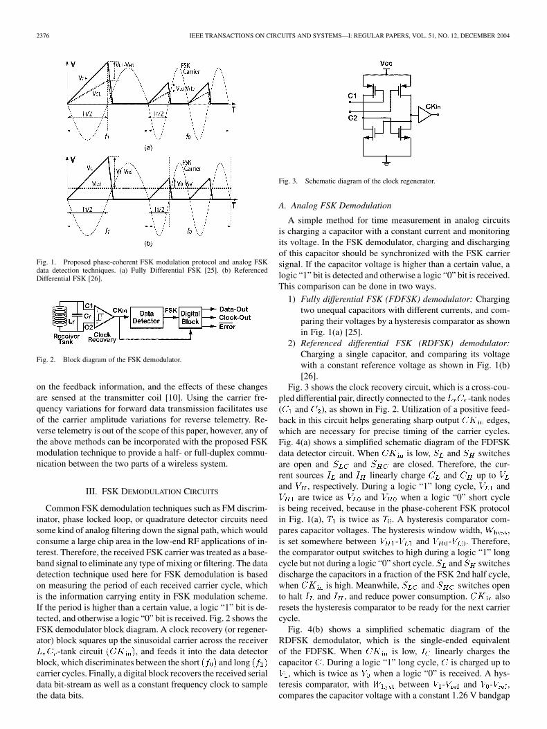
Fig. 3. Schematic diagram of the clock regenerator.
A. Analog FSK Demodulation
A simple method for time measurement in analog circuitsis charging a capacitor with a constant current and monitoringits voltage. In the FSK demodulator, charging and dischargingof this capacitor should be synchronized with the FSK carriersignal. If the capacitor voltage is higher than a certain value, alogic “1” bit is detected and otherwise a logic “0” bit is received.This comparison can be done in two ways.
1) Fully differential FSK (FDFSK) demodulator: Chargingtwo unequal capacitors with different currents, and com-paring their voltages by a hysteresis comparator as shownin Fig. 1(a) [25].
2) Referenced differential FSK (RDFSK) demodulator:Charging a single capacitor, and comparing its voltagewith a constant reference voltage as shown in Fig. 1(b)[26].
Fig. 3 shows the clock recovery circuit, which is a cross-cou-pled differential pair, directly connected to the -tank nodes( and ), as shown in Fig. 2. Utilization of a positive feed-back in this circuit helps generating sharp output edges,which are necessary for precise timing of the carrier cycles.Fig. 4(a) shows a simplified schematic diagram of the FDFSKdata detector circuit. When is low, and switchesare open and and are closed. Therefore, the cur-rent sources and linearly charge and up toand , respectively. During a logic “1” long cycle, and
are twice as and when a logic “0” short cycleis being received, because in the phase-coherent FSK protocolin Fig. 1(a), is twice as . A hysteresis comparator com-pares capacitor voltages. The hysteresis window width, ,is set somewhere between - and - . Therefore,the comparator output switches to high during a logic “1” longcycle but not during a logic “0” short cycle. and switchesdischarge the capacitors in a fraction of the FSK 2nd half cycle,when is high. Meanwhile, and switches opento halt and , and reduce power consumption. alsoresets the hysteresis comparator to be ready for the next carriercycle.
Fig. 4(b) shows a simplified schematic diagram of theRDFSK demodulator, which is the single-ended equivalentof the FDFSK. When is low, linearly charges thecapacitor . During a logic “1” long cycle, is charged up to
, which is twice as when a logic “0” is received. A hys-teresis comparator, with between - and - ,compares the capacitor voltage with a constant 1.26 V bandgap
GHOVANLOO AND NAJAFI: WIDEBAND FSK WIRELESS LINK 2377
Fig. 4. Simplified schematic diagrams of (a) FDFSK and (b) RDFSK datadetector circuits.
Fig. 5. Schematic diagram of the digital block.
reference. The comparator output switches to high during logic“1” but not logic “0”. Finally, discharges in a fraction ofthe carrier second half cycle, when is high, meanwhile,
opens to reduce power consumption by halting .The output of the FDFSK or RDFSK data detector blocks,
called FSK, is only a series of pulses, which discriminate be-tween long and short FSK carrier cycles. Thus, it cannot be di-rectly regarded as the received data bit-stream. These pulses arefed into a digital block, shown in Fig. 5, along with to gen-erate the serial data output (Data-Out) and constant frequencyclock (Clock-Out). On every rising edge of the , a 2-bitshift register shifts in the status of the FSK signal. Every 2 suc-cessive short cycles should be regarded as a “0” bit on Data-Out,and every single long cycle indicates a “1” bit. Any odd numberof short cycles is an indication of error according to the FSK pro-tocol, and activates the error flag (Error ). To generate a constantfrequency clock, a T flip-flop indicates the number of successivezeros, and another T flip-flop toggles on every long cycleor two successive short cycles. The resulting clock fre-quency is constant at irrespective of the data contents. Dig-ital block is designed asynchronously to minimize the number
of gates and consequently the circuit area, as well as desensitizeit to or Clock-out timing jitter. Therefore, signal propaga-tion and timings were considered carefully, and delay elementswere added, before the Clock-Out buffer for example, to avoidmetastable operation of the following digital circuitry that aresupposed to sample and decode the serial data bit-stream [18].
B. Digital FSK Demodulation
In a digital approach for FSK demodulation, the duration ofthe carrier cycles are measured with a constant-frequency clocktime-base at a rate several times higher than the carrierfrequencies ( and ) [27]. Most often, , which does notneed to be synchronized with the carrier, is already availablein the system for running other digital blocks such as a mi-crocontroller. An -bit counter runs while the carrier is “posi-tive” and measures half of a carrier cycle. When the carrier goes“negative”, the counter stops, and a digital comparator decideswhether a long or short carrier cycle is received by comparingthe count value with a constant reference number. Then it resetsthe counter for measuring the duration of the next cycle.
It is necessary for the time-base period to be smallerthan the time-difference between and half-cycles to enablethe demodulator to discriminate between these two frequencies.In other words, should be
(2)
In addition, the minimum width of the counter should satisfy
(3)
In order to simplify the demodulator circuit, and reduce dy-namic power consumption, the digital comparator can be com-bined with the counter by choosing , and such that
(4)
In this case, the most significant bit (MSB) of the counter deter-mines whether a long or short carrier cycle is received, and theconstant reference number would be .
Based on the proposed FSK modulation protocol, fabricationprocess parameters, and required bandwidth for a visual im-plant, and were chosen equal to 8 and 4 MHz, respec-tively. A lower limit for the time-base clock, MHz,is set by (2). By choosing , (4) defines a new range for
64 MHz MHz, which satisfies (2) and (3) aswell. Therefore, a 5-stage ring-oscillator was designed to gen-erate MHz at the center of the above range to providethe maximum level of robustness. It should be noted that as longas is in the desired range, the phase noise and process- ortemperature-dependent frequency variations of the ring oscil-lator do not affect the demodulator performance.
Fig. 6 shows the schematic diagram of the DFSK demod-ulator, and Fig. 7 shows sample simulation waveforms when“00111100110011” data bit-stream trace-1 is FSK modulatedand applied to the DFSK demodulator circuit . The clock re-covery block squares up the received FSK carrier, and generates
. The 5-stage ring-oscillator generates at 49 MHz,
2378 IEEE TRANSACTIONS ON CIRCUITS AND SYSTEMS—I: REGULAR PAPERS, VOL. 51, NO. 12, DECEMBER 2004
Fig. 6. Schematic diagram of the DFSK demodulator.
Fig. 7. Simulated waveforms of the DFSK demodulator.
which runs the 3-bit counter after being gated by .When is high, the counter is running, and it resets when
is low. The counter MSB stays low during short (62.5 ns)carrier half-cycles when , however, it goes high duringlong (125 ns) carrier half-cycles when count . Thecounter resets during the 2nd carrier half-cycle to be ready fordetecting the type of the next cycle. The MSB signal cannotbe directly regarded as the received serial data bit-stream. There-fore, these pulses are fed into the digital block (Fig. 5) alongwith to generate Data-Out and Clock-Out .
IV. WIDEBAND INDUCTIVE LINK
A. Required Bandwidth
Detailed design of the inductive link for biomedical implantscan be found in [1]–[5]. All of these inductive links, except for[5], are designed to maximize the gain and power-transmissionefficiency of the link at the expense of a narrow bandwidth byusing high- LC tanks, tuned at the carrier frequency, on bothtransmitter and receiver sides. Therefore, they are only suitablefor narrowband ASK carriers, which is not the case in the pro-posed FSK modulation scheme. Carlson’s rule approximates thebandwidth (BW) needed to include 98% of the total power of anFM signal [24]:
(5)
where is the maximum frequency shift caused by modula-tion, and is the maximum frequency content of the modu-lating signal. In the proposed FSK protocol, with
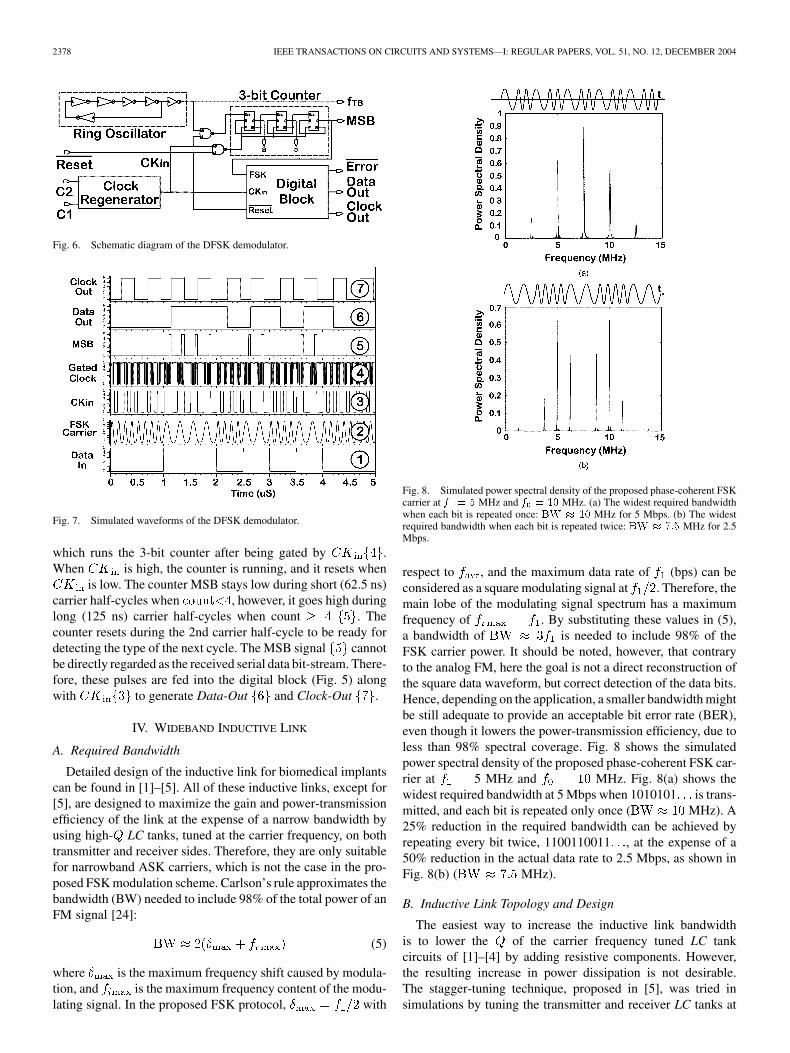
Fig. 8. Simulated power spectral density of the proposed phase-coherent FSKcarrier at f = 5 MHz and f = 10 MHz. (a) The widest required bandwidthwhen each bit is repeated once: BW � 10 MHz for 5 Mbps. (b) The widestrequired bandwidth when each bit is repeated twice: BW � 7:5 MHz for 2.5Mbps.
respect to , and the maximum data rate of (bps) can beconsidered as a square modulating signal at . Therefore, themain lobe of the modulating signal spectrum has a maximumfrequency of . By substituting these values in (5),a bandwidth of is needed to include 98% of theFSK carrier power. It should be noted, however, that contraryto the analog FM, here the goal is not a direct reconstruction ofthe square data waveform, but correct detection of the data bits.Hence, depending on the application, a smaller bandwidth mightbe still adequate to provide an acceptable bit error rate (BER),even though it lowers the power-transmission efficiency, due toless than 98% spectral coverage. Fig. 8 shows the simulatedpower spectral density of the proposed phase-coherent FSK car-rier at 5 MHz and MHz. Fig. 8(a) shows thewidest required bandwidth at 5 Mbps when 1010101 is trans-mitted, and each bit is repeated only once ( MHz). A25% reduction in the required bandwidth can be achieved byrepeating every bit twice, 1100110011 , at the expense of a50% reduction in the actual data rate to 2.5 Mbps, as shown inFig. 8(b) ( MHz).
B. Inductive Link Topology and Design
The easiest way to increase the inductive link bandwidthis to lower the of the carrier frequency tuned LC tankcircuits of [1]–[4] by adding resistive components. However,the resulting increase in power dissipation is not desirable.The stagger-tuning technique, proposed in [5], was tried insimulations by tuning the transmitter and receiver LC tanks at
GHOVANLOO AND NAJAFI: WIDEBAND FSK WIRELESS LINK 2379
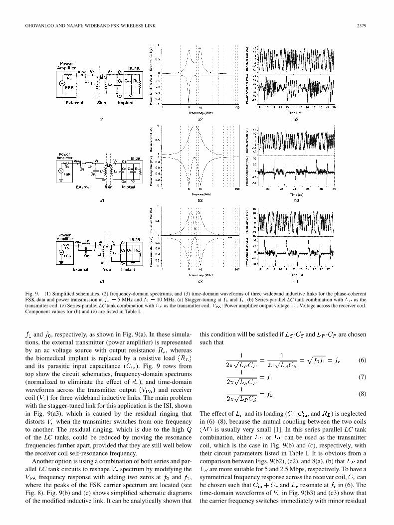
Fig. 9. (1) Simplified schematics, (2) frequency-domain spectrums, and (3) time-domain waveforms of three wideband inductive links for the phase-coherentFSK data and power transmission at f = 5 MHz and f = 10 MHz. (a) Stagger-tuning at f and f . (b) Series-parallel LC tank combination with L as thetransmitter coil. (c) Series-parallel LC tank combination with L as the transmitter coil. V : Power amplifier output voltage V . Voltage across the receiver coil.Component values for (b) and (c) are listed in Table I.
and , respectively, as shown in Fig. 9(a). In these simula-tions, the external transmitter (power amplifier) is representedby an ac voltage source with output resistance , whereasthe biomedical implant is replaced by a resistive loadand its parasitic input capacitance . Fig. 9 rows fromtop show the circuit schematics, frequency-domain spectrums(normalized to eliminate the effect of ), and time-domainwaveforms across the transmitter output and receivercoil for three wideband inductive links. The main problemwith the stagger-tuned link for this application is the ISI, shownin Fig. 9(a3), which is caused by the residual ringing thatdistorts when the transmitter switches from one frequencyto another. The residual ringing, which is due to the highof the LC tanks, could be reduced by moving the resonancefrequencies further apart, provided that they are still well belowthe receiver coil self-resonance frequency.
Another option is using a combination of both series and par-allel LC tank circuits to reshape spectrum by modifying the
frequency response with adding two zeros at and ,where the peaks of the FSK carrier spectrum are located (seeFig. 8). Fig. 9(b) and (c) shows simplified schematic diagramsof the modified inductive link. It can be analytically shown that
this condition will be satisfied if - and - are chosensuch that
(6)
(7)
(8)
The effect of and its loading ( , and ) is neglectedin (6)–(8), because the mutual coupling between the two coils
is usually very small [1]. In this series-parallel LC tankcombination, either or can be used as the transmittercoil, which is the case in Fig. 9(b) and (c), respectively, withtheir circuit parameters listed in Table I. It is obvious from acomparison between Figs. 9(b2), (c2), and 8(a), (b) that and
are more suitable for 5 and 2.5 Mbps, respectively. To have asymmetrical frequency response across the receiver coil, canbe chosen such that and resonate at in (6). Thetime-domain waveforms of in Fig. 9(b3) and (c3) show thatthe carrier frequency switches immediately with minor residual
2380 IEEE TRANSACTIONS ON CIRCUITS AND SYSTEMS—I: REGULAR PAPERS, VOL. 51, NO. 12, DECEMBER 2004
TABLE ICIRCUIT PARAMETERS OF WIRELESS LINK
ringing, which is small enough not to distort the received wave-form in a way that the FSK demodulator cannot detect the cor-rect data bit [compare with in Fig. 9(a3)]. Fig. 9(b3) and (c3)also shows that and are suppressed in , and there areonly spikes at the frequency switching points due to the otherunsuppressed frequency components that become significant atthese points. This suppression reduces the amplifier power dissi-pation by reducing its output voltage, thus improving the overallpower-transmission efficiency.
Yet, another method to establish a wideband inductive linkfor the aforementioned FSK demodulators is to setup a dual-frequency, class-E FSK transmitter, which is introduced in [28].
V. MEASUREMENT RESULTS
The FDFSK demodulator was implemented in an in-house3- m, 1M/2P BiCMOS process [29] to be integrated on micro-electrode arrays that were fabricated in the same process [23].Despite high process-dependent parameter variations in a mul-tipurpose academic facility, satisfactory results were achieved,and reported in [25]. The RDFSK and DFSK demodulators,along with an integrated full-wave rectifier [30], were includedin a prototype chip for a wireless stimulating microsystem, andfabricated in the AMI 1.5- m, 2M/2P standard CMOS process,which is shown in Fig. 10, [26], [27]. With a 5-V supply, theon-chip ring-oscillator generates MHz, which isvery close to the target value of 49 MHz. According to (4), withthis value, the DFSK demodulator works with FSK carriersfrom MHz to MHz. Therefore, even thoughthe chip was designed for a MHz carrier, as discussed inSection III-B and simulated in Fig. 7, a 5/10-MHz carrier wasused in measurements to achieve a higher data rate.
To measure the wideband inductive link characteristics, thecircuit shown in Fig. 9(c1) was utilized with the power ampli-fier replaced with a function generator (Agilent 33 250 A), gen-erating a 20-V sinusoid. To measure the generator outputcurrent , a 10- resistor was added in series with the gen-erator 50- output, and was measured after this resistor
Fig. 10. Die micrograph of the RDFSK and DFSK demodulators,implemented in a prototype chip [26], [27].
60 . The wideband inductive link was set up ac-cording to the specifications listed in Table I, with the series-par-allel LC tank combination connected to the generator by a pairof short wires. In practice, the effect of longer cables should beconsidered in calculating and values, using the transmissionline theory [31]. Fig. 11(a) shows the generator output voltageand current as well as the voltages across transmitter
and receiver coils versus carrier frequency.The transmitter output power ,where is the phase delay between and , and the resis-tive load received power were calculated,and shown in Fig. 11(b) along with the inductive link efficiency,
% , all in the frequency domain. A comparisonbetween Fig. 8(b), , and spectrums in Fig. 11(a) and (b),and simulated waveform in Fig. 9(c3) shows that the de-signed wideband inductive link is capable of transmitting thesignificant frequency components of the proposed FSK carrierwith the gain and power efficiency that is about 25%–50% ofthe narrow-band methods [1]–[5], while minimizing distortionand ISI. It is also important to note that in the near field, the gainand efficiency of the inductive link are strong functions of therelative coils distance. Fig. 11(c) shows measured and at 5and 10 MHz versus in 2–14 mm range.
To evaluate the overall performance of the DFSK demod-ulator and the wireless link, a square-shaped digital FSKsignal was generated on a PC platform, based on the proposedFSK protocol, using a high-speed digital I/O card (NationalInstruments DAQ-6534) in LabView environment. The digitalFSK signal, which has a 2.5-V dc component, passes through adc-level adjustment circuit and bandpass filter (0.01–10 MHz),which reject its dc and high frequency components, and turn itinto a bipolar sinusoidal FSK signal, before being amplified bya wideband power amplifier (Amplifier Research 25A250A).The amplified FSK carrier is then transmitted through theinductive link setup. , which can be inductively coupled toeither or , picks up the FSK carrier, and applies it to therectifier and demodulator blocks. Depending on , the poweramplifier gain was adjusted such that the on-chip rectifier dcoutput, filtered by an off-chip 10-nF capacitor, supplied the
GHOVANLOO AND NAJAFI: WIDEBAND FSK WIRELESS LINK 2381
Fig. 11. Wideband inductive link measured characteristics. (a) V : Voltageacross L ; V : Voltage across series-parallel LC tank combination, V :Voltage across L , and I : Current through LC tank combination versuscarrier frequency. (b) Transmitter power, received power, and inductive linkefficiency versus carrier frequency. (c) V and inductive link efficiency at 5 and10 MHz versus relative L and L coils distance.
entire chip at 5 V. In Fig. 12, the received FSK carrier, measureddifferentially across the -tank, is shown on the 3 lowertraces 30 V . The bandpass filter on the transmitter sideattenuates slightly more than , which causes some am-plitude modulation on the received carrier, when the inductivelink spectrum is quite symmetrical, as in Fig. 9(b) and (c). Thisamplitude modulation can be eliminated in practice by tuningthe -tank resonance frequency closer to , as shown inFig. 11(a). Even though a maximum data rate of Mbpscan be transmitted by a 5/10-MHz carrier, according to the pro-posed FSK protocol, the practical inductive link bandwidth wasnot enough for a full-speed data rate with high enough BER.
Fig. 12. Measured waveforms of the DFSK at 2.5 Mbps with f and f equalto 10 and 5 MHz, respectively. From top: Clock-Out, Data-Out [5 V/div], andsingle ended (C ;C ) and differential (C -C ) carrier voltage at across thereceiver L C tank circuit [20 V/div].
TABLE IIMEASURED RESULTS AND SPECIFICATIONS OF FSK DEMODULATOR CIRCUITS
Therefore, the data rate was reduced to 2.5 Mbps by repeatingevery bit twice, as shown in Fig. 8(b), and the receiver coilwas coupled to to achieve a . The two uppertraces in Fig. 12 show the recovered clock (Clock-Out) anddemodulated serial data bit-stream (Data-Out) at 2.5 MHz and2.5 Mbps, respectively. To measure the BER, several millionbits were generated, transmitted across the wireless link, andrecorded on a different computer, which was connected to theDFSK demodulator, for at least five times. The recorded serialdata bit-streams were then compared to the original, off-line,to calculate the average BER. To the authors’ knowledge, thisis the fastest data rate ever reported in inductively coupledwireless applications [5]–[13].
Table II compares the measured results and specificationsof the three demodulator circuits that were discussed in Sec-tion III. All these circuits are designed for the highest data rateachievable in their fabrication processes, without optimizationin terms of power or chip area consumption. With this criterion,the DFSK circuit seems to offer the best performance. How-ever, it should be noted that with a different set of design cri-teria, the optimal choice might be different. For example, if ahigh data rate to carrier frequency ratio is sought by using a car-rier frequency in the 100-kHz range, then in Fig. 4(b) can bemuch smaller, and the RDFSK demodulator would be the mostpower-efficient solution. On the other hand, the FDFSK methodis the most robust against process variations because of its dif-ferential nature, at the expense of more power consumption.
2382 IEEE TRANSACTIONS ON CIRCUITS AND SYSTEMS—I: REGULAR PAPERS, VOL. 51, NO. 12, DECEMBER 2004
VI. SUMMARY
We have developed a high-rate phase-coherent FSK modula-tion protocol, a wideband inductive link, and three FSK demod-ulator circuits for wireless operation of the inductively powereddevices in need of high data rates, such as stimulating micro-electrode arrays with over 1000 stimulating sites. The phase-coherent FSK modulation/demodulation technique, which hasseveral advantages over the typical ASK method, can also beused in other applications such as RFID tags and smartcardsby adding a mechanism for back telemetry. A wideband induc-tive link is designed by using a series-parallel LC tank combi-nation, between a pair of loosely coupled coils to receive theFSK carrier signal across the receiver coil without significantdistortion. In the demodulator circuit, a serial data bit-streamand a constant frequency clock are extracted from the FSK car-rier, which can be in the 1–25 MHz range, and also powersthe chip after being rectified. The FDFSK demodulator is fab-ricated in the 1M/2P, 3- m UM-BiCMOS process, occupying0.67 mm . The RDFSK and DFSK demodulators are fabricatedin the AMI 2M/2P, 1.5- m standard CMOS process, occupying0.41 and 0.29 mm , respectively. The measurement and simula-tion results, which are summarized in Table II, suggest that theDFSK demodulator is the best choice for achieving the highestdata rate. However, with different design criteria, the analog ap-proaches might be favorable based on the system requirements.By migrating to newer processes with smaller feature size, whileusing the proposed techniques, the main data rate limiting factorseems to be the inductive link bandwidth, and not the speed ofthe demodulator circuitry. It is also possible to narrow down therequired inductive link bandwidth by choosing and closerto one another at the expense of a more complicated synchro-nization scheme.
ACKNOWLEDGMENT
The authors wish to thank Prof. K.D. Wise and Dr. W. J. Heet-derks for their guidance.
REFERENCES
[1] W. H. Ko, S. P. Liang, and C. D. Fung, “Design of radio-frequency pow-ered coils for implant instruments,” Med. Biol. Eng. Comput., vol. 15,pp. 634–640, 1977.
[2] W. J. Heetderks, “RF powering of millimiter- and submillimeter-sizedneural prosthetic implants,” IEEE Trans. Biomed. Eng., vol. 35, pp.323–327, May 1988.
[3] C. M. Zierhofer and E. S. Hochmair, “High-efficiency coupling-insensi-tive transcutaneous power and data transmission via an inductive link,”IEEE Trans. Biomed. Eng., vol. 37, pp. 716–722, July 1990.
[4] , “Geometric approach for coupling enhancement of magneticallycoupled coils,” IEEE Trans. Biomed. Eng., vol. 43, pp. 708–714, July1996.
[5] D. G. Galbraith, M. Soma, and R. L. White, “A wide-band efficient in-ductive transdermal power and data link with coupling insensitive gain,”IEEE Trans. Biomed. Eng., vol. 34, pp. 265–275, Apr. 1987.
[6] C. M. Zierhofer, I. J. Hochmair-Desoyer, and E. S. Hochmair, “Elec-tronic design of a cochlear implant for multichannel high-rate pulsatilestimulation strategies,” IEEE Trans. Rehab. Eng., vol. 3, pp. 112–116,Mar. 1995.
[7] W. Liu et al., “A neuro-stimulus chip with telemetry unit for retinal pros-thetic device,” IEEE J. Solid-State Circuits, vol. 35, pp. 1487–1497, Oct.2001.
[8] G. J. Suaning and N. H. Lovell, “CMOS neuro-stimulation ASIC with100 channels, scalable output, and bidirectional radio-freq. telemetry,”IEEE Trans. Biomed. Eng., vol. 48, pp. 248–260, Feb. 2001.
[9] P. R. Troyk, I. E. Brown, W. H. Moore, and G. E. Loeb, “Develop-ment of BION technology for functional electrical stimulation: Bidi-rectional telemetry,” in Proc. 23rd IEEE-EMBS Conf., vol. 2, 2001, pp.1317–1320.
[10] RFID-Handbook, 2nd ed., K. Finkenzeller, Ed., Wiley, Hoboken, NJ,2003.
[11] A. Abrial, J. Bouvier, M. Renaudin, P. Senn, and P. Vivet, “A new con-tactless smart card IC using an on-chip antenna and an asynchronousmicrocontroller,” IEEE J. Solid-State Circuits, vol. 36, pp. 1101–1107,July 2001.
[12] P. Raker, L. Connell, T. Collins, and D. Russell, “Secure contactlesssmartcard ASIC with DPA protection,” IEEE J. Solid-State Circuits, vol.36, pp. 559–565, Mar. 2001.
[13] P. R. Troyk and M. Edington, “Inductive links and drivers forremotely-powered telemetry systems,” in Proc. Antennas and Propaga-tion Sympo., vol. 1, 2000, pp. 60–62.
[14] K. Cha, K. Horch, and R. A. Normann, “Simulation of a phosphene-based visual field: Visual acuity in a pixelized vision system,” Ann.Biomed. Eng., vol. 20, pp. 439–449, 1992.
[15] J. Weiner. (2003, Dec.) Sight seeing. USC Health Mag. [Online]. Avail-able: http://www.usc.edu/hsc/info/pr/hmm/win03/sight.html
[16] E. Margalit et al., “Retinal prosthesis for the blind,” Survey Ophthalm.,vol. 47, pp. 335–356, 2002.
[17] K. E. Jones and R. A. Normann, “An advanced demultiplexing systemfor physiological stimulation,” IEEE Trans. Biomed. Eng., vol. 44, pp.1210–1220, Dec. 1997.
[18] M. Ghovanloo and K. Najafi, “A modular 32-site wireless neural stimu-lation microsystem,” in Proc. IEEE Int. Solid-State Circuits Conf., Feb.2004, pp. 226–227.
[19] J. C. Lin, “Computer methods for field intensity predictions,” in CRCHandbook of Biological Effects of Electromagnetic Fields, C. Polk andE. Postow, Eds. Boca Raton, FL: CRC, 1986, ch. 2, pp. 273–313.
[20] J. A. Von Arx and K. Najafi, “On-chip coils with integrated cores forremote inductive powering of integrated microsystems,” in Proc. Trans-ducers 1997, June 1997, pp. 999–1002.
[21] M. Ghovanloo, K. Beach, K. D. Wise, and K. Najafi, “A BiCMOS wire-less interface chip for micromachined stimulating microprobes,” in Proc.IEEE EMBS Special Topic Conf. Microtechnology in Medicine and Bi-ology, May 2002, pp. 277–282.
[22] M. Ghovanloo and K. Najafi, “A BiCMOS wireless stimulator chipfor micromachined stimulating microprobes,” in Proc. IEEE 2nd JointEMBS BMES Conf., Oct. 2002, pp. 2113–2114.
[23] M. Ghovanloo, K. D. Wise, and K. Najafi, “Toward a button-sized1024-site wireless cortical microstimulating array,” in Proc. 1st Int.IEEE/EMBS Conf. Neural Engineering, Mar. 2003, pp. 138–141.
[24] G. M. Miller, Modern Electronic Communication, 4th ed. EnglewoodCliffs, NJ: Prentice-Hall, 1993.
[25] M. Ghovanloo and K. Najafi, “A high data transfer rate frequencyshift keying demodulator chip for the wireless biomedical implants,” inProc. IEEE 45th Midwest Symp. Circuits Systems, vol. 3, Aug. 2002,pp. 433–436.
[26] , “A high data-rate frequency shift keying demodulator chip forthe wireless biomedical implants,” in Proc. IEEE Int. Symp. CircuitsSystems, vol. 5, May 2003, pp. 45–48.
[27] , “A fully digital frequency shift keying demodulator chip forthe wireless biomedical implants,” in Proc. IEEE Southwest Symp. onMixed-Signal Design, Feb. 2003, pp. 223–227.
[28] P. R. Troyk and G. A. DeMichele, “Inductively-coupled power and datalink for neural prostheses using a class-E oscillator and FSK modula-tion,” in Proc. IEEE 25th EMBS Conf., Sept. 2003, pp. 3376–3379.
[29] K. D. Wise, D. J. Anderson, J. F. Hetke, D. R. Kipke, and K. Najafi,“Wireless implantable microsystems: High-density electronic interfacesto the nervous system,” Proc. IEEE, vol. 92, pp. 76–97, Jan. 2004.
[30] M. Ghovanloo and K. Najafi, “Fully integrated wideband high-currentrectifiers for inductively powered devices,” IEEE J. Solid-State Circuits,vol. 39, pp. 1976–1984, Nov. 2004.
[31] D. M. Pozar, Microwave Engineering, 2nd ed. New York: Wiley, 1998,ch. 2.
GHOVANLOO AND NAJAFI: WIDEBAND FSK WIRELESS LINK 2383
Maysam Ghovanloo (S’00–M’04) was born in1973. He received the B.S. degree in electricalengineering from the University of Tehran, Tehran,Iran, in 1994, the M.S. (Hons.) degree in biomed-ical engineering from the Amirkabir University ofTechnology, Tehran, Iran, in 1997, and the M.S.and Ph.D. degrees in electrical engineering from theUniversity of Michigan, Ann Arbor, MI, in 2003,and 2004, respectively.
From 1994 to 1998, he worked part-time at theIDEA Inc., Tehran, Iran, where he participated in
the development of the first modular patient care monitoring system in Iran.In December 1998, he founded Sabz-Negar Rayaneh Co. Ltd., to manufacturephysiology and pharmacology research laboratory instruments. In the summerof 2002, he was with the Advanced Bionics Inc., Sylmar, CA, working on thedesign of spinal-cord stimulators. He joined the faculty of North Carolina StateUniversity in August 2004, where he is currently an Assistant Professor in theDepartment of Electrical and Computer Engineering.
Dr. Ghovanloo has received awards in the operational category of the 40thand 41st DAC/ISSCC student design contest in 2003 and 2004, respectively. Heis a member of Tau Beta Pi, the IEEE Solid-State Circuits Society, the IEEE En-gineering in Medicine and Biology Society, and the IEEE Circuits and SystemsSociety.
Khalil Najafi (S’84–M’86–SM’97–F’00) wasborn in 1958. He received the B.S., M.S., and thePh.D. degrees in electrical engineering from theDepartment of Electrical Engineering and ComputerScience, University of Michigan, Ann Arbor, in1980, 1981, and 1986 respectively.
From 1986–1988, he was employed as a ResearchFellow, from 1988–1990, as an Assistant ResearchScientist, from 1990–1993, as an Assistant Pro-fessor, from 1993–1998, as an Associate Professor,and since September 1998, as a Professor and the
Director of the Solid-State Electronics Laboratory, Department of ElectricalEngineering and Computer Science, University of Michigan. His research inter-ests include micromachining technologies, micromachined sensors, actuators,and MEMS; analog integrated circuits; implantable biomedical microsystems;micropackaging; and low-power wireless sensing/actuating systems.
Dr. Najafi was awarded a National Science Foundation Young InvestigatorAward from 1992–1997, was the recipient of the Beatrice Winner Award forEditorial Excellence at the 1986 International Solid-State Circuits Conference,of the Paul Rappaport Award for coauthoring the Best Paper published in theIEEE TRANSACTIONS ON ELECTRON DEVICES, and of the Best Paper Award atISSCC 1999. In 2003, he received the EECS Outstanding Achievement Award,in 2001 he received the Faculty recognition Award, and in 1994 the Universityof Michigan’s “Henry Russel Award” for outstanding achievement and scholar-ship, and was selected as the “Professor of the Year” in 1993. In 1998, he wasnamed the Arthur F. Thurnau Professor for outstanding contributions to teachingand research, and received the College of Engineering’s Research ExcellenceAward. He has been active in the field of solid-state sensors and actuators formore than 20 years, and has been involved in several conferences and work-shops dealing with solid-state sensors and actuators, including the InternationalConference on Solid-State Sensors and Actuators, the Hilton-Head Solid-StateSensors and Actuators Workshop, and the IEEE/ASME Micro Electromechan-ical Systems (MEMS) Conference. Dr. Najafi is the Editor of Solid-State Sen-sors of IEEE TRANSACTIONS ON ELECTRON DEVICES, an Associate Editor ofthe Journal of Micromechanics and Microengineering, and an Editor for theJournal of Sensors and Materials. He also served as the Associate Editor ofIEEE JOURNAL OF SOLID-STATE CIRCUITS from 2000–2004, and the associateeditor for IEEE TRANSACTIONS ON BIOMEDICAL ENGINEERING from 1999 to2000.