May 2007 Rev 2 1/55 55 STMPE2401 24-bit Enhanced port expander with Keypad and PWM controller Xpander logic Features ■ 24 GPIOs ■ Operating voltage 1.8V ■ Hardware key pad controller (8*12 matrix max) ■ 3 PWM (8 bit) output for LED brightness control and blinking ■ Interrupt output (open drain) pin ■ Configurable hotkey feature on each GPIO ■ Ultra-low Standby-mode current ■ Package TFBGA - 36 pins 3.6x3.6mm, pitch 0.5mm Description The STMPE2401 is a GPIO (General Purpose Input / output) port expander able to interface a Main Digital ASIC via the two-line bidirectional bus (I2C); separate GPIO Expander IC is often used in Mobile-Multimedia platforms to solve the problems of the limited amounts of GPIOs usually available on the Digital Engine. The STMPE2401 offers great flexibility as each I/Os is configurable as input, output or specific functions; it's able to scan a keyboard, also provides PWM outputs for brightness control in backlight, rotator decoder interface and GPIO. This device has been designed very low quiescent current, and is including a wake up feature for each I/O, to optimize the power consumption of the IC. Potential application of the STMPE2401 includes portable media player, game console, mobile phone, smart phone TFBGA www.st.com Figure 1. Device summary Part number Package Packaging STMPE2401TBR TFBGA36 Tape and reel
Transcript
May 2007 Rev 2 1/55
55
STMPE240124-bit Enhanced port expander with Keypad and PWM controller
Xpander logic
Features 24 GPIOs
Operating voltage 1.8V
Hardware key pad controller (8*12 matrix max)
3 PWM (8 bit) output for LED brightness control and blinking
Interrupt output (open drain) pin
Configurable hotkey feature on each GPIO
Ultra-low Standby-mode current
Package TFBGA - 36 pins 3.6x3.6mm, pitch 0.5mm
DescriptionThe STMPE2401 is a GPIO (General Purpose Input / output) port expander able to interface a Main Digital ASIC via the two-line bidirectional bus (I2C); separate GPIO Expander IC is often used in Mobile-Multimedia platforms to solve the problems of the limited amounts of GPIOs usually available on the Digital Engine.
The STMPE2401 offers great flexibility as each I/Os is configurable as input, output or specific functions; it's able to scan a keyboard, also provides PWM outputs for brightness control in backlight, rotator decoder interface and GPIO. This device has been designed very low quiescent current, and is including a wake up feature for each I/O, to optimize the power consumption of the IC.
Potential application of the STMPE2401 includes portable media player, game console, mobile phone, smart phone
D2 XTALIN A XTAL Oscillator or External 32KHz input
D1 XTALOUT A XTAL Oscillator
Table 1. Pin assignment
Ball Name Type Name and function
Pin settings STMPE2401
8/55
2.3 GPIO Pin functions
Table 2. GPIO Pin functions
Pin N° NamePrimary Function
Alternate Function 1 Alternate Function 2 Alternate Function 3
2 KP_X0 GPIO 0 Keypad input 0
4 KP_X1 GPIO 1 Keypad input 1
5 KP_X2 GPIO 2 Keypad input 2
6 KP_X3 GPIO 3 Keypad input 3
7 KP_X4 GPIO 4 Keypad input 4
8 KP_X5 GPIO 5 Keypad input 5
9 KP_X6 GPIO 6 Keypad input 6
12 KP_X7 GPIO 7 Keypad input 7
13 KP_Y5 GPIO 13 Keypad output 5
14 KP_Y4 GPIO 12 Keypad output 4
15 KP_Y3 GPIO 11 Keypad output 3
16 KP_Y2 GPIO 10 Keypad output 2
17 KP_Y1 GPIO 9 Keypad output 1
18 KP_Y0 GPIO 8 Keypad output 0
20 ADDR0 GPIO 15
21 KP_Y9 GPIO 18 Keypad output 9 Rotator 0
22 KP_Y10 GPIO 19 Keypad output 10 Rotator 1
23 KP_Y11 GPIO 20 Keypad output 11 Rotator 2
24 PWM3 GPIO 23 Channel 3
25 PWM2 GPIO 22 Channel 2
26 PWM1 GPIO 21 Channel 1
30 KP_Y8 GPIO 17 Keypad output 8 ClkOut
31 KP_Y7 GPIO 16 Keypad output 7
32 KP_Y6 GPIO 14 Keypad output 6
STMPE2401 Pin settings
9/55
2.4 Pin mapping to TFBGA ( bottom view, balls up)
Table 3. Pin mapping to TFBGA
A B C D E F
1 KP-X2 KP-X1 Reset_N XTALOUT SCLK KP-Y6
2 KP-X4 KP-X3 KP-X0 XTALIN SDATA KP-Y7
3 KP-X6 KP-X5 GND GND KP-Y8 INT
4 VCC KP-X7 GND GND PWM-1 VCC
5 KP-Y5 KP-Y3 KP-Y1 KP-Y9 PWM-3 PWM-2
6 KP-Y4 KP-Y2 KP-Y0 ADDR0 KP-Y10 KP-Y11
Maximum rating STMPE2401
10/55
3 Maximum rating
Stressing the device above the rating listed in the “Absolute Maximum Ratings” table may cause permanent damage to the device. These are stress ratings only and operation of the device at these or any other conditions above those indicated in the Operating sections of this specification is not implied. Exposure to Absolute Maximum Rating conditions for extended periods may affect device reliability. Refer also to the STMicroelectronics SURE Program and other relevant quality documents.
All registers have the size of 8-bit. Some of the registers are composed of 2-byte to form 16-bit registers. For each of the module, their registers are residing within the given address range.
The features that are supported by the I2C interface are as below:
I2C Slave device
SDAT and SCLK operates from 1.8V to 3.3V
Compliant to Philip I2C specification version 2.1
Supports Standard (up to 100kbps) and Fast (up to 400kbps) modes.
7-bit device addressing mode
General Call
Start/Restart/Stop
Address up to 4 STMPE2401 devices via I2C
The address is selected by the state of two pins. The state of the pins will be read upon reset and then the pins can be configured for normal operation. The pins will have a pull-up or down to set the address. The I2C interface module allows the connected host system to access the registers in the STMPE2401.
6.1 Start conditionA Start condition is identified by a falling edge of SDATA while SCLK is stable at high state. A Start condition must precede any data/command transfer. The device continuously monitors for a Start condition and will not respond to any transaction unless one is encountered.
6.2 Stop conditionA Stop condition is identified by a rising edge of SDATA while SCLK is stable at high state. A Stop condition terminates communication between the slave device and bus master. A read command that is followed by NoAck can be followed by a Stop condition to force the slave device into idle mode. When the slave device is in idle mode, it is ready to receive the next I2C transaction. A Stop condition at the end of a write command stops the write operation to registers.
6.3 Acknowledge bit (ACK)The acknowledge bit is used to indicate a successful byte transfer. The bus transmitter releases the SDATA after sending eight bits of data. During the ninth bit, the receiver pulls the SDATA low to acknowledge the receipt of the eight bits of data. The receiver may leave the SDATA in high state if it would to not acknowledge the receipt of the data.
STMPE2401 I2C Interface
15/55
6.4 Data inputThe device samples the data input on SDATA on the rising edge of the SCLK. The SDATA signal must be stable during the rising edge of SCLK and the SDATA signal must change only when SCLK is driven low.
6.5 Slave device addressThe slave device address is a 7 address, where the least significant 2-bit are programmable. These 2-bit values will be loaded in once upon reset and after that these 2 pins no longer be needed with the exception during General Call. Up to 4 STMPE2401 devices can be connected on a single I2C bus.
6.6 Memory addressingFor the bus master to communicate to the slave device, the bus master must initiate a Start condition and followed by the slave device address. Accompanying the slave device address, there is a Read/Write bit (R/W). The bit is set to 1 for Read and 0 for Write operation.
If a match occurs on the slave device address, the corresponding device gives an acknowledgement on the SDA during the 9th bit time. If there is no match, it deselects itself from the bus by not responding to the transaction.
Table 12. Slave device address
ADDR 1 ADDR 0 Address
0 0 0x84
0 1 0x86
1 0 0x88
1 1 0x8A
I2C Interface STMPE2401
16/55
6.7 Operation modes
Figure 3. Master/slave operation modes
Table 13. Operating modes
Mode Bytes Programming sequence
Read ≥1
START, Device Address, R/W = 0, Register Address to be read
RESTART, Device Address, R/W = 1, Data Read, STOP
If no STOP is issued, the Data Read can be continuously preformed. If the register address falls within the range that allows address auto-increment, then register address auto-increments internally after every byte of data being read. For register address that falls within a non-incremental address range, the address will be kept static throughout the entire read operations. Refer to the Memory Map table for the address ranges that are auto and non-increment. An example of such a non-increment address is FIFO.
Write ≥1
START, Device Address, R/W=0, Register Address to be written, Data Write, STOP
If no STOP is issued, the Data Write can be continuously performed. If the register address falls within the range that allows address auto-increment, then register address auto-increments internally after every byte of data being written in. For register address that falls within a non-incremental address range, the address will be kept static throughout the entire write operations. Refer to the Memory Map table for the address ranges that are auto and non-increment. An example of a non-increment address is Data Port for initializing the PWM commands.
STMPE2401 I2C Interface
17/55
Figure 4. I2C timing
Table 14. I2C address
Symbol Parameter Min Typ Max Unit
fSCL SCL clock frequency 0 400 kHz
tLOW Clock low period 1.3 µs
tHIGH Clock high period 600 ns
tF SDA and SCL fall time 300 ns
tHD:STASTART condition hold time (After this period the first clock is generated)
600 ns
tSU:STASTART condition setup time (Only relevant for a repeated start period)
600 ns
tSU:DAT Data setup time 100 ns
tHD:DAT Data hold time 0 µs
tSU:STO STOP condition setup time 600 ns
tBUFTime the bust must be free before a new trasmission can start
1.3 µs
System controller STMPE2401
18/55
7 System controller
The system controller is the heart of the STMPE2401. It contains the registers for power control, and the registers for chip identification.
0 Enable_ROT Writing a ‘0’ to this bit will gate off the clock to the Rotator module, thus stopping its operation
1 Enable_KPC Writing a ‘0’ to this bit will gate off the clock to the Keypad Controller module, thus stopping its operation
2 Enable_PWM Writing a ‘0’ to this bit will gate off the clock to the PWM module, thus stopping its operation
3 Enable_GPIO Writing a ‘0’ to this bit will gate off the clock to the GPIO module, thus stopping its operation
4 Sleep Writing a ‘1’ to this bit will put the device in sleep mode. When in sleep mode, all the units which need to work on clocks synchronous to 32KHz will get the clocks derived from the 32K domain. The RC Oscillator will be shut off.
5 Disable_32KHz Set this bit to disable the 32KHz OSC, thus putting the device in hibernate mode. Only a Reset or a wakeup on IIC will reset this bit
6 - -
7 Soft_Reset Writing a ‘1’ to this bit will do a soft reset of the device. Once the reset is done, this bit will be cleared to ‘0’ by the HW.
System controller STMPE2401
20/55
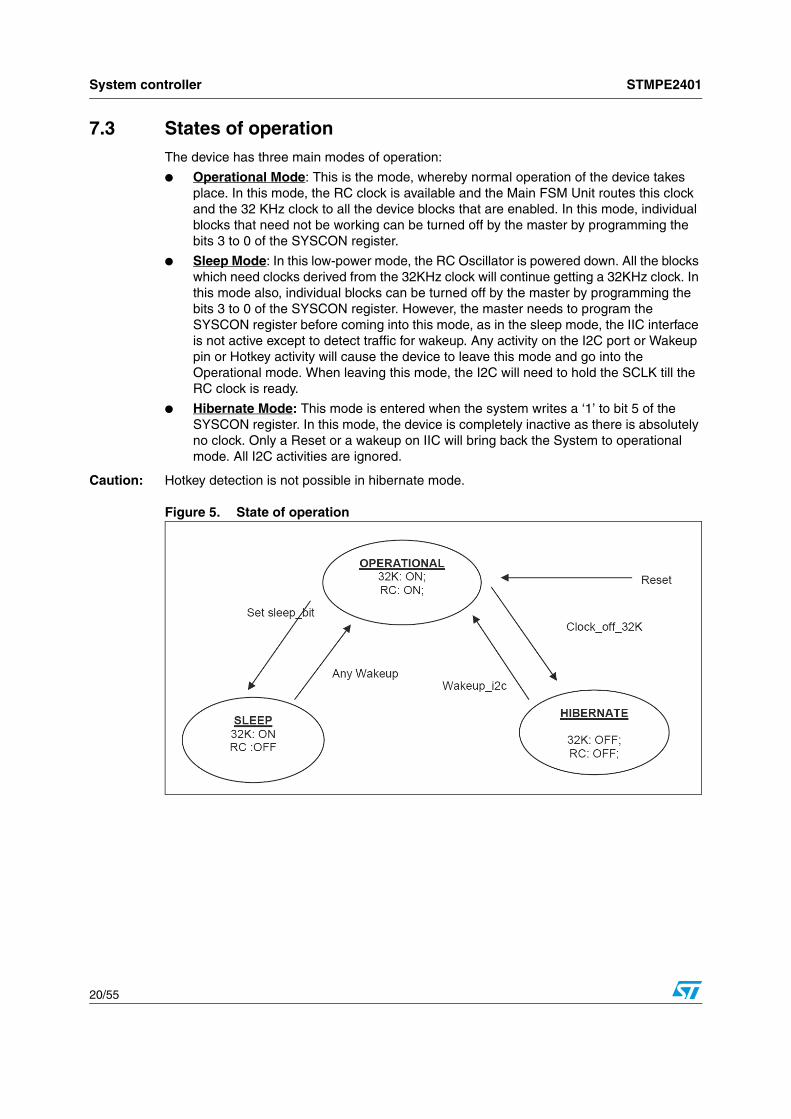
7.3 States of operationThe device has three main modes of operation:
Operational Mode: This is the mode, whereby normal operation of the device takes place. In this mode, the RC clock is available and the Main FSM Unit routes this clock and the 32 KHz clock to all the device blocks that are enabled. In this mode, individual blocks that need not be working can be turned off by the master by programming the bits 3 to 0 of the SYSCON register.
Sleep Mode: In this low-power mode, the RC Oscillator is powered down. All the blocks which need clocks derived from the 32KHz clock will continue getting a 32KHz clock. In this mode also, individual blocks can be turned off by the master by programming the bits 3 to 0 of the SYSCON register. However, the master needs to program the SYSCON register before coming into this mode, as in the sleep mode, the IIC interface is not active except to detect traffic for wakeup. Any activity on the I2C port or Wakeup pin or Hotkey activity will cause the device to leave this mode and go into the Operational mode. When leaving this mode, the I2C will need to hold the SCLK till the RC clock is ready.
Hibernate Mode: This mode is entered when the system writes a ‘1’ to bit 5 of the SYSCON register. In this mode, the device is completely inactive as there is absolutely no clock. Only a Reset or a wakeup on IIC will bring back the System to operational mode. All I2C activities are ignored.
Caution: Hotkey detection is not possible in hibernate mode.
Figure 5. State of operation
STMPE2401 Clocking system
21/55
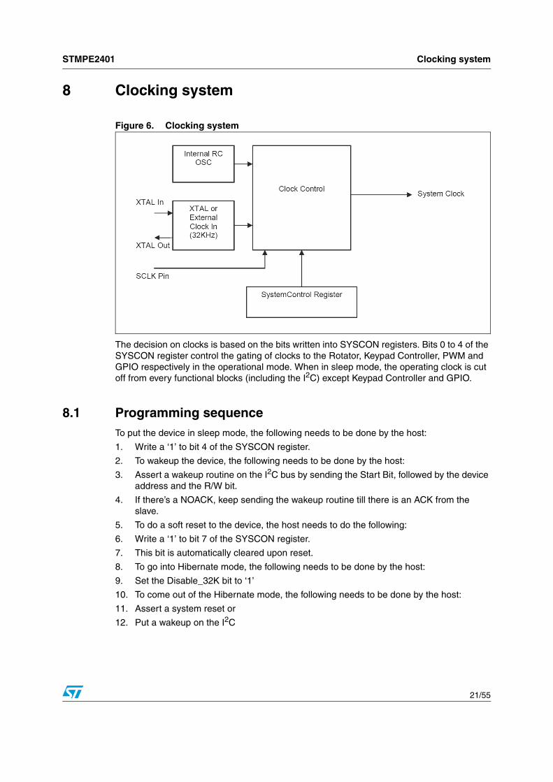
8 Clocking system
Figure 6. Clocking system
The decision on clocks is based on the bits written into SYSCON registers. Bits 0 to 4 of the SYSCON register control the gating of clocks to the Rotator, Keypad Controller, PWM and GPIO respectively in the operational mode. When in sleep mode, the operating clock is cut off from every functional blocks (including the I2C) except Keypad Controller and GPIO.
8.1 Programming sequenceTo put the device in sleep mode, the following needs to be done by the host:
1. Write a ‘1’ to bit 4 of the SYSCON register.
2. To wakeup the device, the following needs to be done by the host:
3. Assert a wakeup routine on the I2C bus by sending the Start Bit, followed by the device address and the R/W bit.
4. If there’s a NOACK, keep sending the wakeup routine till there is an ACK from the slave.
5. To do a soft reset to the device, the host needs to do the following:
6. Write a ‘1’ to bit 7 of the SYSCON register.
7. This bit is automatically cleared upon reset.
8. To go into Hibernate mode, the following needs to be done by the host:
9. Set the Disable_32K bit to ‘1’
10. To come out of the Hibernate mode, the following needs to be done by the host:
11. Assert a system reset or
12. Put a wakeup on the I2C
Interrupt system STMPE2401
22/55
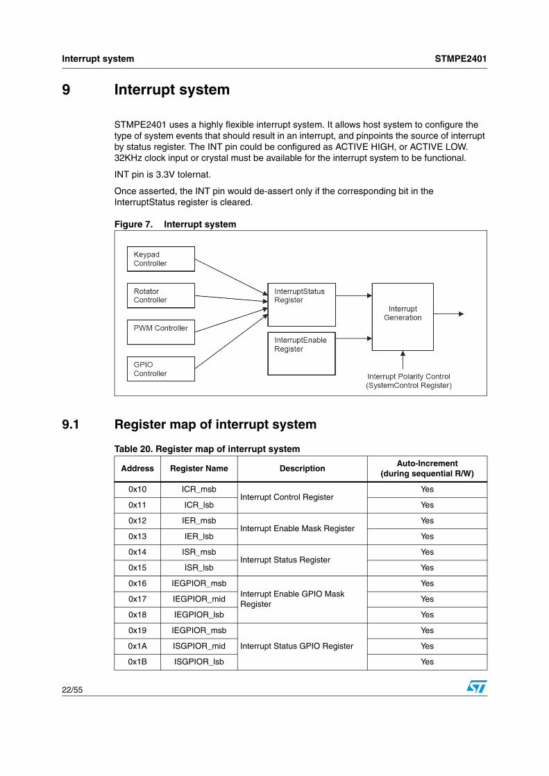
9 Interrupt system
STMPE2401 uses a highly flexible interrupt system. It allows host system to configure the type of system events that should result in an interrupt, and pinpoints the source of interrupt by status register. The INT pin could be configured as ACTIVE HIGH, or ACTIVE LOW. 32KHz clock input or crystal must be available for the interrupt system to be functional.
INT pin is 3.3V tolernat.
Once asserted, the INT pin would de-assert only if the corresponding bit in the InterruptStatus register is cleared.
9.2 Interrupt control register (ICR)ICR register is used to configure the Interrupt Controller. It has a global enable interrupt mask bit that controls the interruption to the host.
9.3 Interrupt enable mask register (IER)IER register is used to enable the interruption from a particular interrupt source to the host.
ICR_msb ICR_lsb
Bit 15 14 13 12 11 10 9 8 7 6 5 4 3 2 1 0
Reserved IC2 IC1 IC0
R/W R R R R R R R R R R R R R RW RW RW
ResetValue
0 0 0 0 0 0 0 0 0 0 0 0 0 0 0 0
Table 21. ICR
Bits Name Description
0 IC[0] Global Interrupt Mask bitWhen this bit is written a ‘1’, it will allow interruption to the host. If it is written with a ‘0’, then, it disables all interruption to the host. Writing to this bit does not affect the IER value.
2 IC[2] output Interrupt Polarity‘0’ = Active Low / Falling Edge‘1’ = Active High / Rising Edge
IER_msb IER_lsb
Bit 15 14 13 12 11 10 9 8 7 6 5 4 3 2 1 0
Reserved IE8 IE7 IE6 IE5 IE4 IE3 IE2 IE1 IE0
R/W R R R R R R R RW RW RW RW RW RW RW RW RW
ResetValue
0 0 0 0 0 0 0 0 0 0 0 0 0 0 0 0
Interrupt system STMPE2401
24/55
9.4 Interrupt status register (ISR)ISR register monitors the status of the interruption from a particular interrupt source to the host. Regardless whether the IER bits are enabled or not, the ISR bits are still updated.
Table 22. IER
Bits Name Description
8:0 IE[x] Interrupt Enable Mask (where x = 8 to 0)IE0 = Wake-up Interrupt MaskIE1 = Keypad Controller Interrupt MaskIE2 = Keypad Controller FIFO Overflow Interrupt MaskIE3 = Rotator Controller Interrupt MaskIE4 = Rotator Controller Buffer Overflow Interrupt MaskIE5 = PWM Channel 0 Interrupt MaskIE6 = PWM Channel 1 Interrupt MaskIE7 = PWM Channel 2 Interrupt MaskIE8 = GPIO Controller Interrupt MaskWriting a ‘1’ to the IE[x] bit will enable the interruption to the host.
ISR_msb ISR_lsb
Bit 15 14 13 12 11 10 9 8 7 6 5 4 3 2 1 0
Reserved IS8 IS7 IS6 IS5 IS4 IS3 IS2 IS1 IS0
R/W R R R R R R R RW RW RW RW RW RW RW RW RW
ResetValue
0 0 0 0 0 0 0 0 0 0 0 0 0 0 0 0
Table 23. ISR
Bits Name Description
8:0 IS[x] Interrupt Status (where x = 8 to 0)Read:IS0 = Wake-up Interrupt StatusIS1 = Keypad Controller Interrupt StatusIS2 = Keypad Controller FIFO Overflow Interrupt StatusIS3 = Rotator Controller Interrupt StatusIS4 = Rotator Controller Buffer Overflow Interrupt StatusIS5 = PWM Channel 0 Interrupt StatusIS6 = PWM Channel 1 Interrupt StatusIS7= PWM Channel 2 Interrupt StatusIS8 = GPIO Controller Interrupt StatusWrite:A write to a IS[x] bit with a value of ‘1’ will clear the interrupt and a write with a value of ‘0’ has no effect on the IS[x] bit.
STMPE2401 Interrupt system
25/55
9.5 Interrupt enable GPIO mask register (IEGPIOR)IEGPIOR register is used to enable the interruption from a particular GPIO interrupt source to the host. The IEG[15:0] bits are the interrupt enable mask bits correspond to the GPIO[15:0] pins.
23:0 IEG[x] Interrupt Enable GPIO Mask (where x = 23 to 0)Writing a ‘1’ to the IE[x] bit will enable the interruption to the host.
Interrupt system STMPE2401
26/55
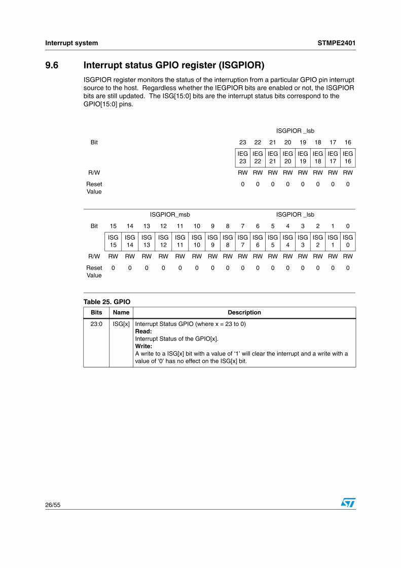
9.6 Interrupt status GPIO register (ISGPIOR)ISGPIOR register monitors the status of the interruption from a particular GPIO pin interrupt source to the host. Regardless whether the IEGPIOR bits are enabled or not, the ISGPIOR bits are still updated. The ISG[15:0] bits are the interrupt status bits correspond to the GPIO[15:0] pins.
23:0 ISG[x] Interrupt Status GPIO (where x = 23 to 0)Read:Interrupt Status of the GPIO[x].Write:A write to a ISG[x] bit with a value of ‘1’ will clear the interrupt and a write with a value of ‘0’ has no effect on the ISG[x] bit.
STMPE2401 Interrupt system
27/55
9.7 Programming sequenceTo configure and initialize the Interrupt Controller to allow interruption to host, observe the following steps:
Set the IER and IEGPIOR registers to the desired values to enable the interrupt sources that are to be expected to receive from.
Configure the output interrupt type and polarity and enable the global interrupt mask by writing to the ICR.
Wait for interrupt.
Upon receiving an interrupt, the INT pin is asserted.
The host comes to read the ISR through I2C interface. A ‘1’ in the ISR bits indicates that the corresponding interrupt source is triggered.
If the IS8 bit in ISR is set, the interrupt is coming from the GPIO Controller. Then, a subsequent read is performed on the ISGPIOR to obtain the interrupt status of all 16 GPIOs to locate the GPIO that triggers the interrupt. This is a feature so-called ‘Hot Key’.
After obtaining the interrupt source that triggers the interrupt, the host performs the necessary processing and operations related to the interrupt source.
If the interrupt source is from the GPIO Controller, two write operations with value of ‘1’ are performed to the ISG[x] bit (ISGPIOR) and the IS[8] (ISR) to clear the corresponding GPIO interrupt.
If the interrupt source is from other module, a write operation with value of ‘1’ is performed to the IS[x] (ISR) to clear the corresponding interrupt.
Once the interrupt is being cleared, the INT pin will also be de-asserted if the interrupt type is level interrupt. An edge interrupt will only assert a pulse width of 250ns.
When the interrupt is no longer required, the IC0 bit in ICR may be set to ‘0’ to disable the global interrupt mask bit.
GPIO controller STMPE2401
28/55
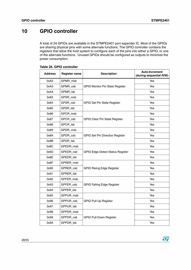
10 GPIO controller
A total of 24 GPIOs are available in the STMPE2401 port expander IC. Most of the GPIOs are sharing physical pins with some alternate functions. The GPIO controller contains the registers that allow the host system to configure each of the pins into either a GPIO, or one of the alternate functions. Unused GPIOs should be configured as outputs to minimize the power consumption.
Table 26. GPIO controller
Address Register name DescriptionAuto-Increment
(during sequential R/W)
0xA2 GPMR_msb
GPIO Monitor Pin State Register
Yes
0xA3 GPMR_csb Yes
0xA4 GPMR_lsb Yes
0x83 GPSR_msb
GPIO Set Pin State Register
Yes
0x84 GPSR_csb Yes
0x85 GPSR_lsb Yes
0x86 GPCR_msb
GPIO Clear Pin State Register
Yes
0x87 GPCR_csb Yes
0x88 GPCR_lsb Yes
0x89 GPDR_msb
GPIO Set Pin Direction Register
Yes
0x8A GPDR_csb Yes
0x8B GPDR_lsb Yes
0x8C GPEDR_msb
GPIO Edge Detect Status Register
Yes
0x8D GPEDR_csb Yes
0x8E GPEDR_lsb Yes
0x8F GPRER_msb
GPIO Rising Edge Register
Yes
0x90 GPRER_csb Yes
0x91 GPRER_lsb Yes
0x92 GPFER_msb
GPIO Falling Edge Register
Yes
0x93 GPFER_csb Yes
0x94 GPFER_lsb Yes
0x95 GPPUR_msb
GPIO Pull Up Register
Yes
0x96 GPPUR_csb Yes
0x97 GPPUR_lsb Yes
0x98 GPPDR_msb
GPIO Pull Down Register
Yes
0x99 GPPDR_csb Yes
0x9A GPPDR_lsb Yes
STMPE2401 GPIO controller
29/55
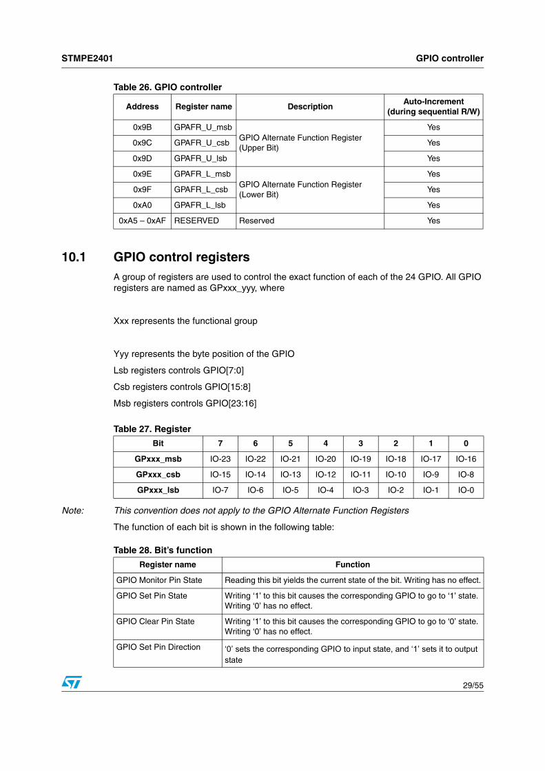
10.1 GPIO control registersA group of registers are used to control the exact function of each of the 24 GPIO. All GPIO registers are named as GPxxx_yyy, where
Xxx represents the functional group
Yyy represents the byte position of the GPIO
Lsb registers controls GPIO[7:0]
Csb registers controls GPIO[15:8]
Msb registers controls GPIO[23:16]
Note: This convention does not apply to the GPIO Alternate Function Registers
The function of each bit is shown in the following table:
Address Register name DescriptionAuto-Increment
(during sequential R/W)
0x9B GPAFR_U_msbGPIO Alternate Function Register (Upper Bit)
Yes
0x9C GPAFR_U_csb Yes
0x9D GPAFR_U_lsb Yes
0x9E GPAFR_L_msbGPIO Alternate Function Register (Lower Bit)
GPIO Monitor Pin State Reading this bit yields the current state of the bit. Writing has no effect.
GPIO Set Pin State Writing ‘1’ to this bit causes the corresponding GPIO to go to ‘1’ state. Writing ‘0’ has no effect.
GPIO Clear Pin State Writing ‘1’ to this bit causes the corresponding GPIO to go to ‘0’ state. Writing ‘0’ has no effect.
GPIO Set Pin Direction ‘0’ sets the corresponding GPIO to input state, and ‘1’ sets it to output state
GPIO controller STMPE2401
30/55
10.2 GPIO alternate function register (GPAFR)GPAFR is to select the functionality of the GPIO pin. To select a function for a GPIO pin, a bit-pair in the register (GPAFR_U or GPAFR_L) has to be set.
Register name Function
GPIO Edge Detect Status Set to ‘1’ by hardware when there is a rising/falling edge on the corre-sponding GPIO. Writing ‘1’ clears the bit. Writing ‘0’ has no effect.
GPIO Rising Edge Set to ‘1’ to enable rising edge detection on the corresponding GPIO.
GPIO Falling Edge Set to ‘1’ to enable falling edge detection on the corresponding GPIO.
GPIO Pull Up Set to ‘1’ to enable internal pull-up resistor
GPIO Pull Down Set to ‘1’ to enable internal pull-down resistor
Table 28. Bit’s function
GPAFR_U_msb
Bit 23 22 21 20 19 18 17 16
AF23 AF22 AF21 AF20
R/W RW RW RW RW RW RW RW RW
Reset Value
0 0 0 0 0 0 0 0
GPAFR_U_csb
Bit 15 14 13 12 11 10 9 8
AF19 AF18 AF17 AF16
R/W RW RW RW RW RW RW RW RW
Reset Value
0 0 0 0 0 0 0 0
GPAFR_U_lsb
Bit 7 6 5 4 3 2 1 0
AF15 AF14 AF13 AF12
R/W RW RW RW RW RW RW RW RW
Reset Value
0 0 0 0 0 0 0 0
STMPE2401 GPIO controller
31/55
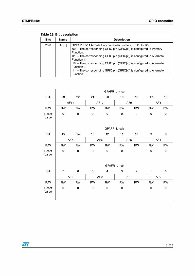
Table 29. Bit description
Bits Name Description
23:0 AF[x] GPIO Pin ‘x’ Alternate Function Select (where x = 23 to 12).‘00’ – The corresponding GPIO pin (GPIO[x]) is configured to Primary Function.‘01’ – The corresponding GPIO pin (GPIO[x]) is configured to Alternate Function 1.‘10’ – The corresponding GPIO pin (GPIO[x]) is configured to Alternate Function 2.‘11’ – The corresponding GPIO pin (GPIO[x]) is configured to Alternate Function 3.
GPAFR_L_msb
Bit 23 22 21 20 19 18 17 16
AF11 AF10 AF9 AF8
R/W RW RW RW RW RW RW RW RW
Reset Value
0 0 0 0 0 0 0 0
GPAFR_L_csb
Bit 15 14 13 12 11 10 9 8
AF7 AF6 AF5 AF4
R/W RW RW RW RW RW RW RW RW
Reset Value
0 0 0 0 0 0 0 0
GPAFR_L_lsb
Bit 7 6 5 4 3 2 1 0
AF3 AF2 AF1 AF0
R/W RW RW RW RW RW RW RW RW
Reset Value
0 0 0 0 0 0 0 0
GPIO controller STMPE2401
32/55
10.3 Hot key featureA GPIO is known as ‘Hot Key’ when it is configured to trigger an interruption to the host whenever the GPIO input is being asserted. This feature is applicable in Operational mode (RC clock is present) as well as Sleep mode (32kHz clock is present).
10.3.1 Programming sequence for hot key
1. Configures the GPIO pin into GPIO mode by setting the corresponding bits in the GPAFR.
2. Configures the GPIO pin into input direction by setting the corresponding bit in GPDR.
3. Set the GPRER and GPFER to the desired values to enable the rising edge or falling edge detection.
4. Configures and enables the interrupt controller to allow the interruption to the host.
5. Now, the GPIO Expander may be put into Sleep mode if it is desired.
6. Upon any Hot Key being asserted, the device will wake-up and issue an interrupt to the host.
Below are the conditions to be fulfilled in order to configure a Hot Key:
1. The pin is configured into GPIO mode and as input pin.
2. The global interrupt mask bit is enabled.
3. The corresponding GPIO interrupt mask bit is enabled.
10.3.2 Minimum pulse width
The minimum pulse width of the assertion of the Hot Key must be at least 62.5us. Any pulse width less than the stated value may not be registered.
Table 30. Bit description
Bits Name Description
23:0 AF[x] GPIO Pin ‘x’ Alternate Function Select (where x = 11 to 0).‘00’ – The corresponding GPIO pin (GPIO[x]) is configured to Primary Function.‘01’ – The corresponding GPIO pin (GPIO[x]) is configured to Alternate Function 1.‘10’ – The corresponding GPIO pin (GPIO[x]) is configured to Alternate Function 2.‘11’ – The corresponding GPIO pin (GPIO[x]) is configured to Alternate Function 3.
STMPE2401 PWM controller
33/55
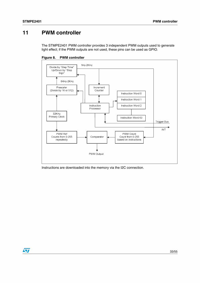
11 PWM controller
The STMPE2401 PWM controller provides 3 independent PWM outputs used to generate light effect; if the PWM outputs are not used, these pins can be used as GPIO.
Figure 8. PWM controller
Instructions are downloaded into the memory via the I2C connection.
PWM controller STMPE2401
34/55
11.1 Registers in the PWM controllerThe main system registers are:
Table 31. Main system registers
Address Register Name DescriptionAuto-Increment
(during Read/Write)
0x30 PWMCS PWM Control and Status register Yes
0x38 PWMIC0
PWM instructions are initialized through this data port. Every instruction is 16-bit width and therefore, the MSB of the first word is written first, then, followed by LSB of the first word. Subsequently, MSB of second word and LSB of second word and so on.
No
0x39 PWMIC1
PWM instructions are initialized through this data port. Every instruction is 16-bit width and therefore, the MSB of the first word is written first, then, followed by LSB of the first word. Subsequently, MSB of second word and LSB of second word and so on.
No
0x3A PWMIC2
PWM instructions are initialized through this data port. Every instruction is 16-bit width and therefore, the MSB of the first word is written first, then, followed by LSB of the first word. Subsequently, MSB of second word and LSB of second word and so on.
No
STMPE2401 PWM controller
35/55
11.2 PWM control and status register (PWMCS)
Bit 7 6 5 4 3 2 1 0
Reserved II2 II1 II0 EN2 EN1 EN0
Read/Write R R R R R RW RW RW
Reset Value 0 0 0 0 0 0 0 0
Table 32. Bit description
Bits Name Description
0 EN0 PWM Channel 0 Enable bit. ‘1’ – Enable the PWM Channel 0‘0’ – Reset the PWM Channel 0. Only when the PWM channel is in reset state, the stream of commands can be written into its data port, which in this case is PWM_Command_Channel_0.
1 EN1 PWM Channel 1 Enable bit. ‘1’ – Enable the PWM Channel 1‘0’ – Reset the PWM Channel 1. Only when the PWM channel is in reset state, the stream of commands can be written into its data port, which in this case is PWM_Command_Channel_1.
2 EN2 PWM Channel 2 Enable bit. ‘1’ – Enable the PWM Channel 2‘0’ – Reset the PWM Channel 2. Only when the PWM channel is in reset state, the stream of commands can be written into its data port, which in this case is PWM_Command_Channel_2.
3 II0 PWM Invalid Instruction Status bit for PWM Channel 0‘0’ – No invalid command encountered during the instruction execution.‘1’ – Invalid command encountered and this puts the PWM Channel 0 into reset state.
4 II1 PWM Invalid Instruction Status bit for PWM Channel 1‘0’ – No invalid command encountered during the instruction execution.‘1’ – Invalid command encountered and this puts the PWM Channel 1 into reset state.
5 II2 PWM Invalid Instruction Status bit for PWM Channel 2‘0’ – No invalid command encountered during the instruction execution.‘1’ – Invalid command encountered and this puts the PWM Channel 2 into reset state.
PWM controller STMPE2401
36/55
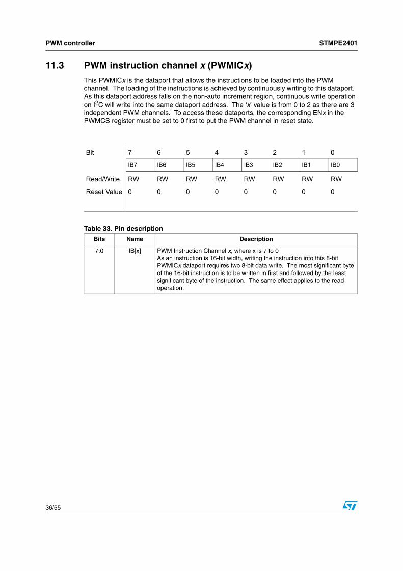
11.3 PWM instruction channel x (PWMICx)This PWMICx is the dataport that allows the instructions to be loaded into the PWM channel. The loading of the instructions is achieved by continuously writing to this dataport. As this dataport address falls on the non-auto increment region, continuous write operation on I2C will write into the same dataport address. The ‘x’ value is from 0 to 2 as there are 3 independent PWM channels. To access these dataports, the corresponding ENx in the PWMCS register must be set to 0 first to put the PWM channel in reset state.
Bit 7 6 5 4 3 2 1 0
IB7 IB6 IB5 IB4 IB3 IB2 IB1 IB0
Read/Write RW RW RW RW RW RW RW RW
Reset Value 0 0 0 0 0 0 0 0
Table 33. Pin description
Bits Name Description
7:0 IB[x] PWM Instruction Channel x, where x is 7 to 0As an instruction is 16-bit width, writing the instruction into this 8-bit PWMICx dataport requires two 8-bit data write. The most significant byte of the 16-bit instruction is to be written in first and followed by the least significant byte of the instruction. The same effect applies to the read operation.
STMPE2401 PWM commands
37/55
12 PWM commands
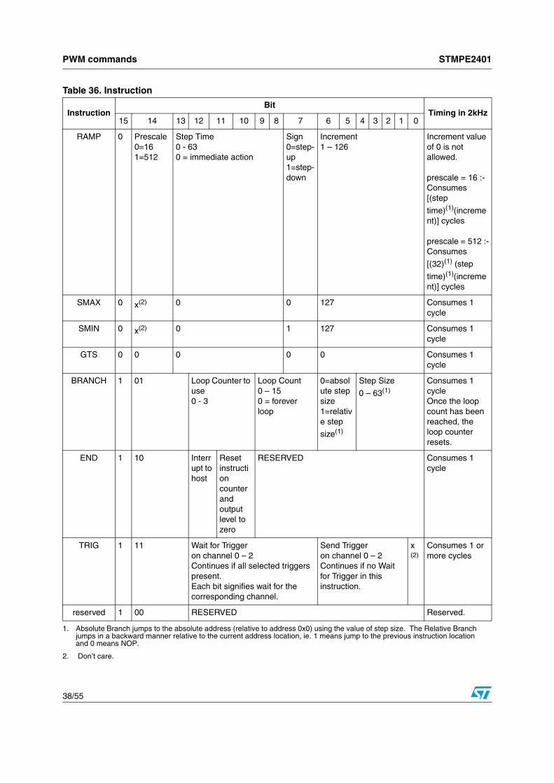
The STMPE2401 PWM Controller works as a simple MCU, with program space of 64 instructions and a simple instruction set. The instructions are all 16 bits in length. The 3 most significant bits are used to identify the commands.
Table 34. PWM commands
Instruction Description
RAMP This instruction starts the PWM counters and set the pwm_x_out with the result from the counting.
Set Maximum (SMAX)
Load the PWM counter with the value of 0xff and the pwm_x_out will result in logic level low.
Set Minimum (SMIN) Load the PWM counter with the value of 0x0 and the pwm_x_out will result in logic level high.
Go to Start (GTS) Branch to the address 0x0 and execute from 0x0 and onwards.
BRANCH Branch to a relative or an absolute address to execute with the looping capability. There are 4 loop counters available and these allow 4 nested loops.
END End the instruction execution by resetting and interrupting to the host.
Trigger (TRIG) Capable of waiting as well as sending triggers to another PWM channel.
0 – 63(1)Consumes 1 cycleOnce the loop count has been reached, the loop counter resets.
END 1 10 Interrupt to host
Reset instruction counter and output level to zero
RESERVED Consumes 1 cycle
TRIG 1 11 Wait for Triggeron channel 0 – 2Continues if all selected triggers present.Each bit signifies wait for the corresponding channel.
Send Triggeron channel 0 – 2Continues if no Wait for Trigger in this instruction.
x(2)
Consumes 1 or more cycles
reserved 1 00 RESERVED Reserved.
1. Absolute Branch jumps to the absolute address (relative to address 0x0) using the value of step size. The Relative Branch jumps in a backward manner relative to the current address location, ie. 1 means jump to the previous instruction location and 0 means NOP.
2. Don’t care.
STMPE2401 PWM commands
39/55
In order to enable a PWM channel, the programming sequence below should be observed.
The ENx of the PWMCS register should be kept in ‘0’. By default, it has a value of ‘0’.
Loads the instructions into the PWM channel x by writing the corresponding PWMICx.
The PWM channel x has a 64-word depth (16-bit width). Any instructions of size less than or equal to 64 words can be loaded into the channel. Any attempt to load beyond 64 words will result in internal address pointer to roll-over (0x1f ◊ 0x00) and the excess instructions to be over-written into the first address location of the channel and onwards.
After the instructions are loaded in, then, the PWM channel x can be enabled by setting a ‘1’ to the ENx bit.
Enables the corresponding interrupt mask bit to allow interruption to the host.
Keypad controller STMPE2401
40/55
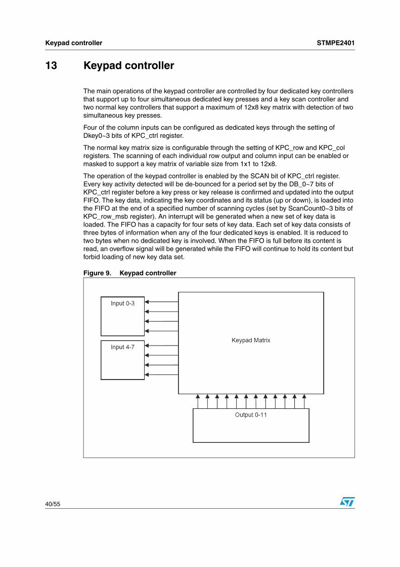
13 Keypad controller
The main operations of the keypad controller are controlled by four dedicated key controllers that support up to four simultaneous dedicated key presses and a key scan controller and two normal key controllers that support a maximum of 12x8 key matrix with detection of two simultaneous key presses.
Four of the column inputs can be configured as dedicated keys through the setting of Dkey0~3 bits of KPC_ctrl register.
The normal key matrix size is configurable through the setting of KPC_row and KPC_col registers. The scanning of each individual row output and column input can be enabled or masked to support a key matrix of variable size from 1x1 to 12x8.
The operation of the keypad controller is enabled by the SCAN bit of KPC_ctrl register. Every key activity detected will be de-bounced for a period set by the DB_0~7 bits of KPC_ctrl register before a key press or key release is confirmed and updated into the output FIFO. The key data, indicating the key coordinates and its status (up or down), is loaded into the FIFO at the end of a specified number of scanning cycles (set by ScanCount0~3 bits of KPC_row_msb register). An interrupt will be generated when a new set of key data is loaded. The FIFO has a capacity for four sets of key data. Each set of key data consists of three bytes of information when any of the four dedicated keys is enabled. It is reduced to two bytes when no dedicated key is involved. When the FIFO is full before its content is read, an overflow signal will be generated while the FIFO will continue to hold its content but forbid loading of new key data set.
Figure 9. Keypad controller
STMPE2401 Keypad controller
41/55
The keypad column inputs enabled by the KPC_col register are normally ‘HIGH’, with the corresponding input pins pulled up by resistors internally. After reset, all the keypad row outputs enabled by the KPC_row register are driven ‘LOW’. If a key is pressed, its corresponding column input will become ‘LOW’ after making contact with the ‘LOW’ voltage on its corresponding row output.
Once the key scan controller senses a ‘LOW’ input on any of the column inputs, the scanning cycles will then start to determine the exact key that has been pressed. The twelve row outputs will be driven ‘LOW’ one by one (if the row output is enabled) during each scanning cycle. While one row is driven ‘LOW’, the other rows are driven ‘HIGH’. (The pull-ups and pull-downs of row outputs are always disabled). If there is any column input sensed as ‘LOW’ when a row is driven ‘LOW’, the key scan controller will then decode the key coordinates (its corresponding row number and column number), save the key data into a de-bounce buffer if available, confirm if it is a valid key press after de-bouncing, and update the key data into output data FIFO if valid.
13.1 Registers in keypad controller
Table 37. Register in keypad controller
Address Register name DescriptionAuto-Increment
(during sequential R/W)
0x60 KPC_col Keypad column scanning register Yes
0x61 KPC_row_msb Keypad row scanning register Yes
0x62 KPC_row_lsb Yes
0x63 KPC_ctrl_msb Keypad control register Yes
0x64 KPC_ctrl_lsb Yes
0x68 KPC_data_byte0 Keypad data register No
0x69 KPC_data_byte1 No
0x6A KPC_data_byte2 No
Keypad controller STMPE2401
42/55
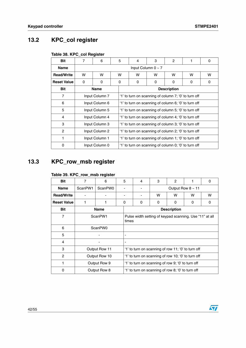
13.2 KPC_col register
13.3 KPC_row_msb register
Table 38. KPC_col Register
Bit 7 6 5 4 3 2 1 0
Name Input Column 0 ~ 7
Read/Write W W W W W W W W
Reset Value 0 0 0 0 0 0 0 0
Bit Name Description
7 Input Column 7 ‘1’ to turn on scanning of column 7; ‘0’ to turn off
6 Input Column 6 ‘1’ to turn on scanning of column 6; ‘0’ to turn off
5 Input Column 5 ‘1’ to turn on scanning of column 5; ‘0’ to turn off
4 Input Column 4 ‘1’ to turn on scanning of column 4; ‘0’ to turn off
3 Input Column 3 ‘1’ to turn on scanning of column 3; ‘0’ to turn off
2 Input Column 2 ‘1’ to turn on scanning of column 2; ‘0’ to turn off
1 Input Column 1 ‘1’ to turn on scanning of column 1; ‘0’ to turn off
0 Input Column 0 ‘1’ to turn on scanning of column 0; ‘0’ to turn off
Table 39. KPC_row_msb register
Bit 7 6 5 4 3 2 1 0
Name ScanPW1 ScanPW0 - - Output Row 8 ~ 11
Read/Write - - - - W W W W
Reset Value 1 1 0 0 0 0 0 0
Bit Name Description
7 ScanPW1 Pulse width setting of keypad scanning. Use “11” at all times
6 ScanPW0
5 - -
4 - -
3 Output Row 11 ‘1’ to turn on scanning of row 11; ‘0’ to turn off
2 Output Row 10 ‘1’ to turn on scanning of row 10; ‘0’ to turn off
1 Output Row 9 ‘1’ to turn on scanning of row 9; ‘0’ to turn off
0 Output Row 8 ‘1’ to turn on scanning of row 8; ‘0’ to turn off
STMPE2401 Keypad controller
43/55
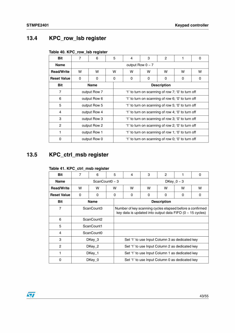
13.4 KPC_row_lsb register
13.5 KPC_ctrl_msb register
Table 40. KPC_row_lsb register
Bit 7 6 5 4 3 2 1 0
Name output Row 0 ~ 7
Read/Write W W W W W W W W
Reset Value 0 0 0 0 0 0 0 0
Bit Name Description
7 output Row 7 ‘1’ to turn on scanning of row 7; ‘0’ to turn off
6 output Row 6 ‘1’ to turn on scanning of row 6; ‘0’ to turn off
5 output Row 5 ‘1’ to turn on scanning of row 5; ‘0’ to turn off
4 output Row 4 ‘1’ to turn on scanning of row 4; ‘0’ to turn off
3 output Row 3 ‘1’ to turn on scanning of row 3; ‘0’ to turn off
2 output Row 2 ‘1’ to turn on scanning of row 2; ‘0’ to turn off
1 output Row 1 ‘1’ to turn on scanning of row 1; ‘0’ to turn off
0 output Row 0 ‘1’ to turn on scanning of row 0; ‘0’ to turn off
Table 41. KPC_ctrl_msb register
Bit 7 6 5 4 3 2 1 0
Name ScanCount0 ~ 3 DKey_0 ~ 3
Read/Write W W W W W W W W
Reset Value 0 0 0 0 0 0 0 0
Bit Name Description
7 ScanCount3 Number of key scanning cycles elapsed before a confirmed key data is updated into output data FIFO (0 ~ 15 cycles)
6 ScanCount2
5 ScanCount1
4 ScanCount0
3 DKey_3 Set ‘1’ to use Input Column 3 as dedicated key
2 DKey_2 Set ‘1’ to use Input Column 2 as dedicated key
1 DKey_1 Set ‘1’ to use Input Column 1 as dedicated key
0 DKey_0 Set ‘1’ to use Input Column 0 as dedicated key
Keypad controller STMPE2401
44/55
13.6 KPC_ctrl_lsb register
13.7 Data registersThe KPC_DATA register contains three bytes of information. The first two bytes store the key coordinates and status of any two keys from the normal key matrix, while the third byte store the status of dedicated keys.
Table 42. KPC_ctrl_lsb register
Bit 7 6 5 4 3 2 1 0
Name DB_0 ~ 5 SCAN
Read/Write W W W W W W W W
Reset Value 0 0 0 0 0 0 0 0
Bit Name Description
7 DB_6 0-128ms of de-bounce time
6 DB_5
5 DB_4
4 DB_3
3 DB_2
2 DB_1
1 DB_0
0 SCAN ‘1’ to start scanning; ‘0’ to stop
Table 43. KPC_data_byte0 register
Bit 7 6 5 4 3 2 1 0
Name Up/Down R3 R2 R1 R0 C2 C1 C0
Read/Write R R R R R R R R
Reset Value 1 1 1 1 1 0 0 0
Bit Name Description
7 Up/Down ‘0’ for key-down, ‘1’ for key-up
6 R3 row number of key 1 (valid range : 0-11)0x1111 for No Key
5 R2
4 R1
3 R0
2 C2 column number of key 1 (valid range : 0-7)
1 C1
0 C0
STMPE2401 Keypad controller
45/55
Table 44. KPC_data_byte1 register
Bit 7 6 5 4 3 2 1 0
Name Up/Down R3 R2 R1 R0 C2 C1 C0
Read/Write R R R R R R R R
Reset Value 1 1 1 1 1 0 0 0
Bit Name Description
7 Up/Down ‘0’ for key-down, ‘1’ for key-up
6 R3 row number of key 2 (valid range : 0-11)0x1111 for No Key
5 R2
4 R1
3 R0
2 C2 column number of key 2 (valid range : 0-7)
1 C1
0 C0
Table 45. KPC_data_byte2 register
Bit 7 6 5 4 3 2 1 0
Name - - - - Dedicated Key 0 ~ 3
Read/Write R R R R R R R R
Reset Value
0 0 0 0 1 1 1 1
Bit Name Description
7 - -
6 - -
5 - -
4 - -
3 Dedicated Key 3 ‘0’ for key-down, ‘1’ for key-up
2 Dedicated Key 2 ‘0’ for key-down, ‘1’ for key-up
1 Dedicated Key 1 ‘0’ for key-down, ‘1’ for key-up
0 Dedicated Key 0 ‘0’ for key-down, ‘1’ for key-up
Keypad controller STMPE2401
46/55
13.7.1 Resistance
Maximum resistance between keypad output and keypad input, inclusive of switch resistance, protection circuit resistance and connection, must be less than 3.2 KΩ
13.7.2 Using the keypad controller
Before enabling the keypad controller operation, proper setup should be done by configuring the input and output ports involved. This is achieved by programming the corresponding GPIO control registers that determine the port direction and the necessary internal pull-up or pull-down. For the GPIO ports that are used as keypad inputs, internal pull-up should be enabled. For those that are used as keypad outputs, no internal pull-up or pull-down should be enabled.
The scanning of column inputs should then be enabled for those GPIO ports that are configured as keypad inputs by writing ‘1’s to the corresponding bits in the KPC_col register. If any of the first three column inputs is to be used as dedicated key input, the corresponding bits in the KPC_ctrl_msb register should be set to ‘1’. The bits in the KPC_row_msb and KPC_row_lsb registers should also be set correctly to enable the row output scanning for the corresponding GPIO ports programmed as keypad outputs.
The scan count and de-bounce count should also be programmed into the keypad control registers before enabling the keypad controller operation. To enable the keypad controller operation, the Enable_KPC bit in the system control register must be set to ‘1’ to provide the required clock signals. The keypad controller will then start its operation by setting the SCAN bit in the KPC_ctrl_lsb register to ‘1’.
The keypad controller operation can be disabled by setting the SCAN bit back to ‘0’. To further reduce the power consumption, the clock signals can be cut off from the keypad controller by setting the Enable_KPC bit to ‘0’.
ScanCount value is programmable to any value between 1-15 by writing into the scancount register. If scan count is programmed to N, the Keypad Controller scans the entire matrix for N times, collecting up to 2 matrix key and 4 dedicated keys, loads the keys into 1 set of keypad data buffer and interrupts the host system.
STMPE2401 Rotator controller
47/55
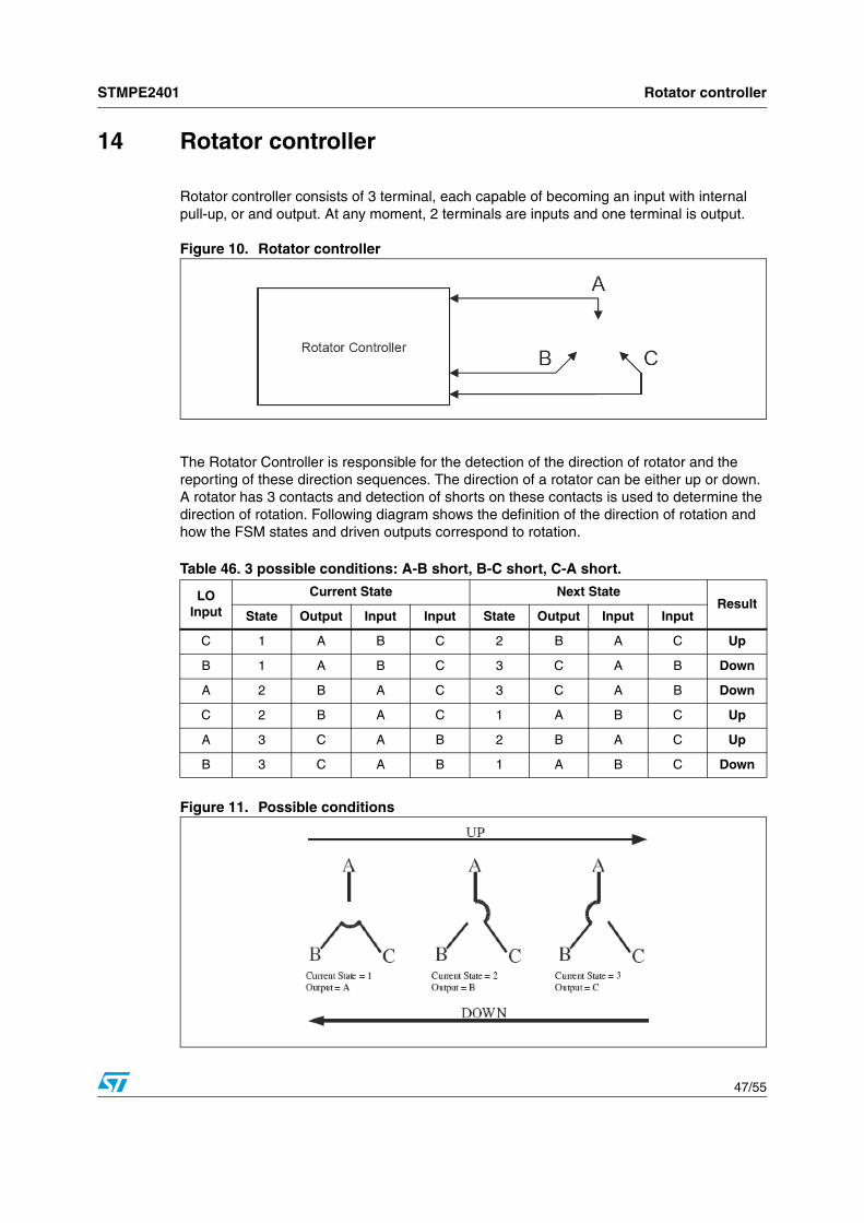
14 Rotator controller
Rotator controller consists of 3 terminal, each capable of becoming an input with internal pull-up, or and output. At any moment, 2 terminals are inputs and one terminal is output.
Figure 10. Rotator controller
The Rotator Controller is responsible for the detection of the direction of rotator and the reporting of these direction sequences. The direction of a rotator can be either up or down. A rotator has 3 contacts and detection of shorts on these contacts is used to determine the direction of rotation. Following diagram shows the definition of the direction of rotation and how the FSM states and driven outputs correspond to rotation.
7 Symbol_Type Symbol type to be reported ‘1’ – Down‘0’ – Up
6~0 Symbol_Count Number of symbols of the type specified by bit 7 Minimum of 0 (b’0000000) toMaximum of 127 (b’1111111)
STMPE2401 Rotator controller
49/55
The host should do the following on the I2C bus to start the Rotator controller:
1. The host writes to GPIO Controller to configure the PU/PD bit and select the Rotator Bits on the relevant IO.
2. Write Rotator_Control data register to start the rotator controller. A maximum of 2 rotations later, the correct initial state on the rotator FSM is obtained. Scanning for rotator movement continues.
3. The host waits for interrupt from the rotator controller.
4. The host reads Rotator_Buffer
5. The host can stop rotator controller operation by writing to Rotator_Control register.
Miscellaneous features STMPE2401
50/55
15 Miscellaneous features
15.1 ResetSTMPE2401 is equipped with an internal POR circuit that holds the device in reset state, until the clock is steady and VCC input is valid. Host system may choose to reset the STMPE2401 by asserting Reset_N pin.
15.2 Under voltage lockoutSTMPE2401 is equipped with an internal UVLO circuit that generates a RESET signal, when the main supply voltage falls below the allowed threshold.
15.3 Clock outputSTMPE2401 provides a buffered 32KHz clock output at one of the GPIO as alternate function. This clock could be used for cascading of multiple port expander devices, using just 1 XTAL unit.
STMPE2401 Mechanical data
51/55
16 Mechanical data
In order to meet environmental requirements, ST offers these devices in ECOPACK® packages. These packages have a Lead-free second level interconnect . The category of second level interconnect is marked on the package and on the inner box label, in compliance with JEDEC Standard JESD97. The maximum ratings related to soldering conditions are also marked on the inner box label. ECOPACK is an ST trademark. ECOPACK specifications are available at: www.st.com
Mechanical data STMPE2401
52/55
Figure 12. Package dimensions
Table 48. TFBGA Mechanical data
Dim.mm. inch
Min Typ Max Min Typ Max
A 1.1 1 1.16 0.043 0.039 0.046
A1 0.25 0.010
A2 0.78 0.86 0.031 0.034
b 0.30 0.25 0.35 0.012 0.010 0.014
D 3.60 3.50 3.70 0.142 0.138 0.146
D1 3.50 0.138
E 3.50 3.60 3.70 0.142 0.138 0.146
E1 2.50 0.098
e 0.50 0.020
F 0.55 0.022
STMPE2401 Mechanical data
53/55
Figure 13. Recommended footprint
Figure 14. Tape and reel information
Revision history STMPE2401
54/55
17 Revision history
Table 49. Revision history
Date Revision Changes
08-Jan-2007 1 Initial release
29-May-2007 2 Cover page updated
STMPE2401
55/55
Please Read Carefully:
Information in this document is provided solely in connection with ST products. STMicroelectronics NV and its subsidiaries (“ST”) reserve theright to make changes, corrections, modifications or improvements, to this document, and the products and services described herein at anytime, without notice.
All ST products are sold pursuant to ST’s terms and conditions of sale.
Purchasers are solely responsible for the choice, selection and use of the ST products and services described herein, and ST assumes noliability whatsoever relating to the choice, selection or use of the ST products and services described herein.
No license, express or implied, by estoppel or otherwise, to any intellectual property rights is granted under this document. If any part of thisdocument refers to any third party products or services it shall not be deemed a license grant by ST for the use of such third party productsor services, or any intellectual property contained therein or considered as a warranty covering the use in any manner whatsoever of suchthird party products or services or any intellectual property contained therein.
UNLESS OTHERWISE SET FORTH IN ST’S TERMS AND CONDITIONS OF SALE ST DISCLAIMS ANY EXPRESS OR IMPLIEDWARRANTY WITH RESPECT TO THE USE AND/OR SALE OF ST PRODUCTS INCLUDING WITHOUT LIMITATION IMPLIEDWARRANTIES OF MERCHANTABILITY, FITNESS FOR A PARTICULAR PURPOSE (AND THEIR EQUIVALENTS UNDER THE LAWSOF ANY JURISDICTION), OR INFRINGEMENT OF ANY PATENT, COPYRIGHT OR OTHER INTELLECTUAL PROPERTY RIGHT.
UNLESS EXPRESSLY APPROVED IN WRITING BY AN AUTHORIZED ST REPRESENTATIVE, ST PRODUCTS ARE NOTRECOMMENDED, AUTHORIZED OR WARRANTED FOR USE IN MILITARY, AIR CRAFT, SPACE, LIFE SAVING, OR LIFE SUSTAININGAPPLICATIONS, NOR IN PRODUCTS OR SYSTEMS WHERE FAILURE OR MALFUNCTION MAY RESULT IN PERSONAL INJURY,DEATH, OR SEVERE PROPERTY OR ENVIRONMENTAL DAMAGE. ST PRODUCTS WHICH ARE NOT SPECIFIED AS "AUTOMOTIVEGRADE" MAY ONLY BE USED IN AUTOMOTIVE APPLICATIONS AT USER’S OWN RISK.
Resale of ST products with provisions different from the statements and/or technical features set forth in this document shall immediately voidany warranty granted by ST for the ST product or service described herein and shall not create or extend in any manner whatsoever, anyliability of ST.
ST and the ST logo are trademarks or registered trademarks of ST in various countries.
Information in this document supersedes and replaces all information previously supplied.
The ST logo is a registered trademark of STMicroelectronics. All other names are the property of their respective owners.
Australia - Belgium - Brazil - Canada - China - Czech Republic - Finland - France - Germany - Hong Kong - India - Israel - Italy - Japan - Malaysia - Malta - Morocco - Singapore - Spain - Sweden - Switzerland - United Kingdom - United States of America