128
Not Recommended for New Designs. Use MC1320x. Document Number: MC13192RM Rev. 1.6 04/2008 MC13192 2.4 GHz Low Power Transceiver for the IEEE ® 802.15.4 Standard Reference Manual

Not Recomm
ended for New Designs.
Use MC1320x.
Document Number: MC13192RMRev. 1.604/2008
MC131922.4 GHz Low Power Transceiverfor the IEEE® 802.15.4 Standard
Reference Manual

Not Recomm
ended for New Designs.
Use MC1320x.
How to Reach Us:
Home Page:www.freescale.com
E-mail:[email protected]
USA/Europe or Locations Not Listed:Freescale SemiconductorTechnical Information Center, CH3701300 N. Alma School RoadChandler, Arizona 85224+1-800-521-6274 or [email protected]
Europe, Middle East, and Africa:Freescale Halbleiter Deutschland GmbHTechnical Information CenterSchatzbogen 781829 Muenchen, Germany+44 1296 380 456 (English)+46 8 52200080 (English)+49 89 92103 559 (German)+33 1 69 35 48 48 (French)[email protected]
Japan:Freescale Semiconductor Japan Ltd.HeadquartersARCO Tower 15F1-8-1, Shimo-Meguro, Meguro-ku,Tokyo 153-0064, Japan0120 191014 or +81 3 5437 [email protected]
Asia/Pacific:Freescale Semiconductor Hong Kong Ltd.Technical Information Center2 Dai King StreetTai Po Industrial EstateTai Po, N.T., Hong Kong+800 2666 [email protected]
For Literature Requests Only:Freescale Semiconductor Literature Distribution CenterP.O. Box 5405Denver, Colorado 802171-800-521-6274 or 303-675-2140Fax: [email protected]
Information in this document is provided solely to enable system and software implementers to use Freescale Semiconductor products. There are no express or implied copyright licenses granted hereunder to design or fabricate any integrated circuits or integrated circuits based on the information in this document.Freescale Semiconductor reserves the right to make changes without further notice to any products herein. Freescale Semiconductor makes no warranty, representation or guarantee regarding the suitability of its products for any particular purpose, nor does Freescale Semiconductor assume any liability arising out of the application or use of any product or circuit, and specifically disclaims any and all liability, including without limitation consequential or incidental damages. “Typical” parameters that may be provided in Freescale Semiconductor data sheets and/or specifications can and do vary in different applications and actual performance may vary over time. All operating parameters, including “Typicals”, must be validated for each customer application by customer’s technical experts. Freescale Semiconductor does not convey any license under its patent rights nor the rights of others. Freescale Semiconductor products are not designed, intended, or authorized for use as components in systems intended for surgical implant into the body, or other applications intended to support or sustain life, or for any other application in which the failure of the Freescale Semiconductor product could create a situation where personal injury or death may occur. Should Buyer purchase or use Freescale Semiconductor products for any such unintended or unauthorized application, Buyer shall indemnify and hold Freescale Semiconductor and its officers, employees, subsidiaries, affiliates, and distributors harmless against all claims, costs, damages, and expenses, and reasonable attorney fees arising out of, directly or indirectly, any claim of personal injury or death associated with such unintended or unauthorized use, even if such claim alleges that Freescale Semiconductor was negligent regarding the design or manufacture of the part.
Freescale™ and the Freescale logo are trademarks of Freescale Semiconductor, Inc. All other product or service names are the property of their respective owners.
© Freescale Semiconductor, Inc. 2005, 2006, 2007, 2008. All rights reserved.

Not Recomm
ended for New Designs.
Use MC1320x.
MC13192 Reference Manual, Rev. 1.6
Freescale Semiconductor iii
ContentsAbout This Book
Audience . . . . . . . . . . . . . . . . . . . . . . . . . . . . . . . . . . . . . . . . . . . . . . . . . . . . . . . . . . . . . . . . . . . . ixOrganization . . . . . . . . . . . . . . . . . . . . . . . . . . . . . . . . . . . . . . . . . . . . . . . . . . . . . . . . . . . . . . . . . ixRevision History . . . . . . . . . . . . . . . . . . . . . . . . . . . . . . . . . . . . . . . . . . . . . . . . . . . . . . . . . . . . . . . xConventions . . . . . . . . . . . . . . . . . . . . . . . . . . . . . . . . . . . . . . . . . . . . . . . . . . . . . . . . . . . . . . . . . . xDefinitions, Acronyms, and Abbreviations . . . . . . . . . . . . . . . . . . . . . . . . . . . . . . . . . . . . . . . . . . xReferences. . . . . . . . . . . . . . . . . . . . . . . . . . . . . . . . . . . . . . . . . . . . . . . . . . . . . . . . . . . . . . . . . . . xi
Chapter 1 Introduction
1.1 Features . . . . . . . . . . . . . . . . . . . . . . . . . . . . . . . . . . . . . . . . . . . . . . . . . . . . . . . . . . . . . . . . . . . . 1-21.2 Software Support . . . . . . . . . . . . . . . . . . . . . . . . . . . . . . . . . . . . . . . . . . . . . . . . . . . . . . . . . . . . 1-21.2.1 Simple MAC (SMAC) . . . . . . . . . . . . . . . . . . . . . . . . . . . . . . . . . . . . . . . . . . . . . . . . . . . . . 1-31.2.2 802.15.4 Standard-Compliant MAC. . . . . . . . . . . . . . . . . . . . . . . . . . . . . . . . . . . . . . . . . . . 1-31.2.3 ZigBee-Compliant Network Stack (BeeStack). . . . . . . . . . . . . . . . . . . . . . . . . . . . . . . . . . . 1-31.3 Block Diagrams . . . . . . . . . . . . . . . . . . . . . . . . . . . . . . . . . . . . . . . . . . . . . . . . . . . . . . . . . . . . . 1-31.4 Data Transfer Modes . . . . . . . . . . . . . . . . . . . . . . . . . . . . . . . . . . . . . . . . . . . . . . . . . . . . . . . . . 1-41.5 Packet Structure . . . . . . . . . . . . . . . . . . . . . . . . . . . . . . . . . . . . . . . . . . . . . . . . . . . . . . . . . . . . . 1-41.6 Receive Path Description . . . . . . . . . . . . . . . . . . . . . . . . . . . . . . . . . . . . . . . . . . . . . . . . . . . . . . 1-51.7 Transmit Path Description . . . . . . . . . . . . . . . . . . . . . . . . . . . . . . . . . . . . . . . . . . . . . . . . . . . . . 1-5
Chapter 2 MC13192 Pins and Connections
2.1 Device Pin Assignment. . . . . . . . . . . . . . . . . . . . . . . . . . . . . . . . . . . . . . . . . . . . . . . . . . . . . . . . 2-12.2 Pin Definitions . . . . . . . . . . . . . . . . . . . . . . . . . . . . . . . . . . . . . . . . . . . . . . . . . . . . . . . . . . . . . . 2-2
Chapter 3 System Considerations
3.1 Introduction. . . . . . . . . . . . . . . . . . . . . . . . . . . . . . . . . . . . . . . . . . . . . . . . . . . . . . . . . . . . . . . . . 3-13.2 Power Connections . . . . . . . . . . . . . . . . . . . . . . . . . . . . . . . . . . . . . . . . . . . . . . . . . . . . . . . . . . . 3-13.3 Test Pin SM . . . . . . . . . . . . . . . . . . . . . . . . . . . . . . . . . . . . . . . . . . . . . . . . . . . . . . . . . . . . . . . . 3-23.4 Reset Usage. . . . . . . . . . . . . . . . . . . . . . . . . . . . . . . . . . . . . . . . . . . . . . . . . . . . . . . . . . . . . . . . . 3-23.5 MC13192 Interface to MCU. . . . . . . . . . . . . . . . . . . . . . . . . . . . . . . . . . . . . . . . . . . . . . . . . . . . 3-33.5.1 SPI Command Channel. . . . . . . . . . . . . . . . . . . . . . . . . . . . . . . . . . . . . . . . . . . . . . . . . . . . . 3-33.5.2 Interrupt Request to MCU . . . . . . . . . . . . . . . . . . . . . . . . . . . . . . . . . . . . . . . . . . . . . . . . . . 3-43.5.3 Modem Control Signals . . . . . . . . . . . . . . . . . . . . . . . . . . . . . . . . . . . . . . . . . . . . . . . . . . . . 3-43.5.4 Modem Status Signals . . . . . . . . . . . . . . . . . . . . . . . . . . . . . . . . . . . . . . . . . . . . . . . . . . . . . 3-43.6 System Oscillator and Clock Considerations . . . . . . . . . . . . . . . . . . . . . . . . . . . . . . . . . . . . . . . 3-43.6.1 Modem Crystal Oscillator. . . . . . . . . . . . . . . . . . . . . . . . . . . . . . . . . . . . . . . . . . . . . . . . . . . 3-43.6.2 System Clock Configurations . . . . . . . . . . . . . . . . . . . . . . . . . . . . . . . . . . . . . . . . . . . . . . . . 3-53.6.3 Single System Crystal with CLKO driving MCU crystal input . . . . . . . . . . . . . . . . . . . . . . 3-63.7 GPIO Characteristics . . . . . . . . . . . . . . . . . . . . . . . . . . . . . . . . . . . . . . . . . . . . . . . . . . . . . . . . . 3-6

Not Recomm
ended for New Designs.
Use MC1320x.
MC13192 Reference Manual, Rev. 1.6
iv Freescale Semiconductor
3.8 MC13192 Digital Signal Properties Summary . . . . . . . . . . . . . . . . . . . . . . . . . . . . . . . . . . . . . . 3-73.9 Transceiver RF Port Operation and External Connections. . . . . . . . . . . . . . . . . . . . . . . . . . . . . 3-83.10 Low Power Considerations . . . . . . . . . . . . . . . . . . . . . . . . . . . . . . . . . . . . . . . . . . . . . . . . . . . . . 3-93.10.1 Modem Low Power States . . . . . . . . . . . . . . . . . . . . . . . . . . . . . . . . . . . . . . . . . . . . . . . . . 3-103.10.2 Special Considerations for Hibernate and Doze Low Power Modes . . . . . . . . . . . . . . . . . 3-113.10.2.1 Doze Current Higher Than Specified . . . . . . . . . . . . . . . . . . . . . . . . . . . . . . . . . . . . . . 3-113.10.2.2 Asserting ATTN Early to Exit Hibernate or Doze Mode . . . . . . . . . . . . . . . . . . . . . . . 3-113.10.3 Recovery Times from Low Power Modes . . . . . . . . . . . . . . . . . . . . . . . . . . . . . . . . . . . . . 3-123.10.3.1 Modem Active Currents . . . . . . . . . . . . . . . . . . . . . . . . . . . . . . . . . . . . . . . . . . . . . . . . 3-133.10.3.1.1 Modem CCA/ED Timing profile . . . . . . . . . . . . . . . . . . . . . . . . . . . . . . . . . . . . . . 3-133.10.3.1.2 Modem RX Timing profile . . . . . . . . . . . . . . . . . . . . . . . . . . . . . . . . . . . . . . . . . . . 3-143.10.3.1.3 Modem TX Timing profile . . . . . . . . . . . . . . . . . . . . . . . . . . . . . . . . . . . . . . . . . . . 3-143.10.4 General System Considerations for Low Power. . . . . . . . . . . . . . . . . . . . . . . . . . . . . . . . . 3-15
Chapter 4 SPI Register Descriptions
4.1 Overview. . . . . . . . . . . . . . . . . . . . . . . . . . . . . . . . . . . . . . . . . . . . . . . . . . . . . . . . . . . . . . . . . . . 4-14.2 Mandatory Register Initialization . . . . . . . . . . . . . . . . . . . . . . . . . . . . . . . . . . . . . . . . . . . . . . . . 4-14.3 Register Model and Description Details . . . . . . . . . . . . . . . . . . . . . . . . . . . . . . . . . . . . . . . . . . . 4-24.4 Reset - Register 00 . . . . . . . . . . . . . . . . . . . . . . . . . . . . . . . . . . . . . . . . . . . . . . . . . . . . . . . . . . . 4-54.5 RX_Pkt_RAM - Register 01. . . . . . . . . . . . . . . . . . . . . . . . . . . . . . . . . . . . . . . . . . . . . . . . . . . . 4-54.6 TX_Pkt_RAM - Register 02 . . . . . . . . . . . . . . . . . . . . . . . . . . . . . . . . . . . . . . . . . . . . . . . . . . . . 4-64.7 TX_Pkt_Ctl - Register 03 . . . . . . . . . . . . . . . . . . . . . . . . . . . . . . . . . . . . . . . . . . . . . . . . . . . . . . 4-74.8 CCA_Thresh - Register 04 . . . . . . . . . . . . . . . . . . . . . . . . . . . . . . . . . . . . . . . . . . . . . . . . . . . . . 4-84.9 IRQ_Mask - Register 05 . . . . . . . . . . . . . . . . . . . . . . . . . . . . . . . . . . . . . . . . . . . . . . . . . . . . . . . 4-94.10 Control_A - Register 06 . . . . . . . . . . . . . . . . . . . . . . . . . . . . . . . . . . . . . . . . . . . . . . . . . . . . . . 4-114.11 Control_B - Register 07 . . . . . . . . . . . . . . . . . . . . . . . . . . . . . . . . . . . . . . . . . . . . . . . . . . . . . . 4-134.12 PA_Enable - Register 08. . . . . . . . . . . . . . . . . . . . . . . . . . . . . . . . . . . . . . . . . . . . . . . . . . . . . . 4-144.13 Control_C - Register 09 . . . . . . . . . . . . . . . . . . . . . . . . . . . . . . . . . . . . . . . . . . . . . . . . . . . . . . 4-154.14 CLKO_Ctl - Register 0A . . . . . . . . . . . . . . . . . . . . . . . . . . . . . . . . . . . . . . . . . . . . . . . . . . . . . 4-164.15 GPIO_Dir - Register 0B . . . . . . . . . . . . . . . . . . . . . . . . . . . . . . . . . . . . . . . . . . . . . . . . . . . . . . 4-174.16 GPIO_Data_Out - Register 0C . . . . . . . . . . . . . . . . . . . . . . . . . . . . . . . . . . . . . . . . . . . . . . . . . 4-194.17 LO1_Int_Div - Register 0F. . . . . . . . . . . . . . . . . . . . . . . . . . . . . . . . . . . . . . . . . . . . . . . . . . . . 4-204.18 LO1_Num - Register 10 . . . . . . . . . . . . . . . . . . . . . . . . . . . . . . . . . . . . . . . . . . . . . . . . . . . . . . 4-214.19 PA_Lvl - Register 12 . . . . . . . . . . . . . . . . . . . . . . . . . . . . . . . . . . . . . . . . . . . . . . . . . . . . . . . . 4-224.20 Tmr_Cmp1_A - Register 1B. . . . . . . . . . . . . . . . . . . . . . . . . . . . . . . . . . . . . . . . . . . . . . . . . . . 4-234.21 Tmr_Cmp1_B - Register 1C. . . . . . . . . . . . . . . . . . . . . . . . . . . . . . . . . . . . . . . . . . . . . . . . . . . 4-234.22 Tmr_Cmp2_A - Register 1D . . . . . . . . . . . . . . . . . . . . . . . . . . . . . . . . . . . . . . . . . . . . . . . . . . 4-254.23 Tmr_Cmp2_B - Register 1E . . . . . . . . . . . . . . . . . . . . . . . . . . . . . . . . . . . . . . . . . . . . . . . . . . . 4-254.24 Tmr_Cmp3_A - Register 1F . . . . . . . . . . . . . . . . . . . . . . . . . . . . . . . . . . . . . . . . . . . . . . . . . . . 4-274.25 Tmr_Cmp3_B - Register 20 . . . . . . . . . . . . . . . . . . . . . . . . . . . . . . . . . . . . . . . . . . . . . . . . . . . 4-274.26 Tmr_Cmp4_A -Register 21 . . . . . . . . . . . . . . . . . . . . . . . . . . . . . . . . . . . . . . . . . . . . . . . . . . . 4-294.27 Tmr_Cmp4_B - Register 22 . . . . . . . . . . . . . . . . . . . . . . . . . . . . . . . . . . . . . . . . . . . . . . . . . . . 4-304.28 TC2_Prime - Register 23 . . . . . . . . . . . . . . . . . . . . . . . . . . . . . . . . . . . . . . . . . . . . . . . . . . . . . 4-31

Not Recomm
ended for New Designs.
Use MC1320x.
MC13192 Reference Manual, Rev. 1.6
Freescale Semiconductor v
4.29 IRQ_Status - Register 24 . . . . . . . . . . . . . . . . . . . . . . . . . . . . . . . . . . . . . . . . . . . . . . . . . . . . . 4-324.30 RST_Ind - Register 25 . . . . . . . . . . . . . . . . . . . . . . . . . . . . . . . . . . . . . . . . . . . . . . . . . . . . . . . 4-344.31 Current_Time_A - Register 26 . . . . . . . . . . . . . . . . . . . . . . . . . . . . . . . . . . . . . . . . . . . . . . . . . 4-354.32 Current_Time_B - Register 27 . . . . . . . . . . . . . . . . . . . . . . . . . . . . . . . . . . . . . . . . . . . . . . . . . 4-354.33 GPIO_Data_In - Register 28. . . . . . . . . . . . . . . . . . . . . . . . . . . . . . . . . . . . . . . . . . . . . . . . . . . 4-364.34 Chip_ID - Register 2C . . . . . . . . . . . . . . . . . . . . . . . . . . . . . . . . . . . . . . . . . . . . . . . . . . . . . . . 4-374.35 RX_Status - Register 2D. . . . . . . . . . . . . . . . . . . . . . . . . . . . . . . . . . . . . . . . . . . . . . . . . . . . . . 4-374.36 Timestamp_A - Register 2E . . . . . . . . . . . . . . . . . . . . . . . . . . . . . . . . . . . . . . . . . . . . . . . . . . . 4-384.37 Timestamp_B - Register 2F . . . . . . . . . . . . . . . . . . . . . . . . . . . . . . . . . . . . . . . . . . . . . . . . . . . 4-384.38 BER_Enable - Register 30 . . . . . . . . . . . . . . . . . . . . . . . . . . . . . . . . . . . . . . . . . . . . . . . . . . . . 4-394.39 PSM_Mode - Register 31 . . . . . . . . . . . . . . . . . . . . . . . . . . . . . . . . . . . . . . . . . . . . . . . . . . . . . 4-40
Chapter 5 Serial Peripheral Interface (SPI)
5.1 Overview. . . . . . . . . . . . . . . . . . . . . . . . . . . . . . . . . . . . . . . . . . . . . . . . . . . . . . . . . . . . . . . . . . . 5-15.2 SPI Basic Operation . . . . . . . . . . . . . . . . . . . . . . . . . . . . . . . . . . . . . . . . . . . . . . . . . . . . . . . . . . 5-15.2.1 SPI Pin Definition. . . . . . . . . . . . . . . . . . . . . . . . . . . . . . . . . . . . . . . . . . . . . . . . . . . . . . . . . 5-15.2.1.1 Chip Enable (CE) . . . . . . . . . . . . . . . . . . . . . . . . . . . . . . . . . . . . . . . . . . . . . . . . . . . . . . 5-25.2.1.2 SPI Clock (SPICLK). . . . . . . . . . . . . . . . . . . . . . . . . . . . . . . . . . . . . . . . . . . . . . . . . . . . 5-25.2.1.3 Master Out / Slave In (MOSI) . . . . . . . . . . . . . . . . . . . . . . . . . . . . . . . . . . . . . . . . . . . . 5-25.2.1.4 Master In / Slave Out (MISO) . . . . . . . . . . . . . . . . . . . . . . . . . . . . . . . . . . . . . . . . . . . . 5-25.2.1.4.1 Setting MISO Output Drive Strength . . . . . . . . . . . . . . . . . . . . . . . . . . . . . . . . . . . . 5-25.2.1.4.2 Setting MISO Off Impedance . . . . . . . . . . . . . . . . . . . . . . . . . . . . . . . . . . . . . . . . . . 5-25.2.2 SPI Burst Operation . . . . . . . . . . . . . . . . . . . . . . . . . . . . . . . . . . . . . . . . . . . . . . . . . . . . . . . 5-35.3 SPI Singular Transactions. . . . . . . . . . . . . . . . . . . . . . . . . . . . . . . . . . . . . . . . . . . . . . . . . . . . . . 5-35.3.1 SPI Singular Transaction Signalling. . . . . . . . . . . . . . . . . . . . . . . . . . . . . . . . . . . . . . . . . . . 5-45.3.2 SPI Singular Transaction Protocol . . . . . . . . . . . . . . . . . . . . . . . . . . . . . . . . . . . . . . . . . . . . 5-45.4 Symbol / Data Format. . . . . . . . . . . . . . . . . . . . . . . . . . . . . . . . . . . . . . . . . . . . . . . . . . . . . . . . . 5-55.5 SPI Recursive Transactions . . . . . . . . . . . . . . . . . . . . . . . . . . . . . . . . . . . . . . . . . . . . . . . . . . . . 5-65.5.1 Recursive SPI Register Read . . . . . . . . . . . . . . . . . . . . . . . . . . . . . . . . . . . . . . . . . . . . . . . . 5-65.5.2 Recursive SPI Register Write . . . . . . . . . . . . . . . . . . . . . . . . . . . . . . . . . . . . . . . . . . . . . . . . 5-65.5.3 Special Case - Packet RAM Access . . . . . . . . . . . . . . . . . . . . . . . . . . . . . . . . . . . . . . . . . . . 5-75.5.3.1 Recursive Receive Packet RAM Read Access . . . . . . . . . . . . . . . . . . . . . . . . . . . . . . . . 5-75.5.3.1.1 Receive Packet RAM Read Access Flow . . . . . . . . . . . . . . . . . . . . . . . . . . . . . . . . . 5-75.5.3.1.2 Receive Packet RAM Read Access Error Conditions . . . . . . . . . . . . . . . . . . . . . . . 5-85.5.3.2 Recursive Transmit Packet RAM Write Access. . . . . . . . . . . . . . . . . . . . . . . . . . . . . . . 5-85.5.3.2.1 Transmit Packet RAM Write Access Flow. . . . . . . . . . . . . . . . . . . . . . . . . . . . . . . . 5-95.5.3.2.2 Transmit Packet RAM Write Access Error Conditions . . . . . . . . . . . . . . . . . . . . . . 5-95.6 Program Reset (Writing Address 0x00) . . . . . . . . . . . . . . . . . . . . . . . . . . . . . . . . . . . . . . . . . . 5-10
Chapter 6 Modes of Operation
6.1 Operational Modes Summary . . . . . . . . . . . . . . . . . . . . . . . . . . . . . . . . . . . . . . . . . . . . . . . . . . . 6-16.2 Low Power Modes . . . . . . . . . . . . . . . . . . . . . . . . . . . . . . . . . . . . . . . . . . . . . . . . . . . . . . . . . . . 6-4

Not Recomm
ended for New Designs.
Use MC1320x.
MC13192 Reference Manual, Rev. 1.6
vi Freescale Semiconductor
6.2.1 Off Mode. . . . . . . . . . . . . . . . . . . . . . . . . . . . . . . . . . . . . . . . . . . . . . . . . . . . . . . . . . . . . . . . 6-46.2.2 Hibernate Mode . . . . . . . . . . . . . . . . . . . . . . . . . . . . . . . . . . . . . . . . . . . . . . . . . . . . . . . . . . 6-46.2.3 Doze Mode . . . . . . . . . . . . . . . . . . . . . . . . . . . . . . . . . . . . . . . . . . . . . . . . . . . . . . . . . . . . . . 6-46.2.3.1 Normal Doze Mode . . . . . . . . . . . . . . . . . . . . . . . . . . . . . . . . . . . . . . . . . . . . . . . . . . . . 6-46.2.3.2 Acoma Doze Mode . . . . . . . . . . . . . . . . . . . . . . . . . . . . . . . . . . . . . . . . . . . . . . . . . . . . . 6-56.3 Active Modes . . . . . . . . . . . . . . . . . . . . . . . . . . . . . . . . . . . . . . . . . . . . . . . . . . . . . . . . . . . . . . . 6-56.3.1 Idle Mode . . . . . . . . . . . . . . . . . . . . . . . . . . . . . . . . . . . . . . . . . . . . . . . . . . . . . . . . . . . . . . . 6-56.3.2 Controlling Transition to Other Active Modes from Idle. . . . . . . . . . . . . . . . . . . . . . . . . . . 6-66.3.3 Packet Mode Data Transfer TX and RX Operation . . . . . . . . . . . . . . . . . . . . . . . . . . . . . . . 6-66.3.3.1 Packet Receive Mode . . . . . . . . . . . . . . . . . . . . . . . . . . . . . . . . . . . . . . . . . . . . . . . . . . . 6-76.3.3.2 Aborting a Packet Receive Sequence . . . . . . . . . . . . . . . . . . . . . . . . . . . . . . . . . . . . . . . 6-86.3.3.3 Packet Transmit Mode . . . . . . . . . . . . . . . . . . . . . . . . . . . . . . . . . . . . . . . . . . . . . . . . . . 6-86.3.4 Stream Mode Data Transfer TX and RX Operation . . . . . . . . . . . . . . . . . . . . . . . . . . . . . . . 6-96.3.4.1 Stream Receive Mode. . . . . . . . . . . . . . . . . . . . . . . . . . . . . . . . . . . . . . . . . . . . . . . . . . 6-116.3.4.2 Aborting a Stream Receive Mode Sequence . . . . . . . . . . . . . . . . . . . . . . . . . . . . . . . . 6-126.3.4.3 Stream Transmit Mode . . . . . . . . . . . . . . . . . . . . . . . . . . . . . . . . . . . . . . . . . . . . . . . . . 6-136.3.5 Clear Channel Assessment (CCA) Modes (including Link Quality Indication) . . . . . . . . 6-146.3.5.1 Clear Channel Assessment Function (use_strm is zero). . . . . . . . . . . . . . . . . . . . . . . . 6-146.3.5.2 Energy Detect Function (use_strm is zero). . . . . . . . . . . . . . . . . . . . . . . . . . . . . . . . . . 6-176.3.5.3 CCA / ED While in Stream Mode (use_strm is one) . . . . . . . . . . . . . . . . . . . . . . . . . . 6-186.3.5.4 Link Quality Indication. . . . . . . . . . . . . . . . . . . . . . . . . . . . . . . . . . . . . . . . . . . . . . . . . 6-186.4 Frequency of Operation . . . . . . . . . . . . . . . . . . . . . . . . . . . . . . . . . . . . . . . . . . . . . . . . . . . . . . 6-186.5 Transmit Power Adjustment . . . . . . . . . . . . . . . . . . . . . . . . . . . . . . . . . . . . . . . . . . . . . . . . . . . 6-196.6 2.4GHz PLL Out-of-Lock Interrupt . . . . . . . . . . . . . . . . . . . . . . . . . . . . . . . . . . . . . . . . . . . . . 6-20
Chapter 7 Timer Information
7.1 Event Timer Block . . . . . . . . . . . . . . . . . . . . . . . . . . . . . . . . . . . . . . . . . . . . . . . . . . . . . . . . . . . 7-17.2 Event Timer Time Base . . . . . . . . . . . . . . . . . . . . . . . . . . . . . . . . . . . . . . . . . . . . . . . . . . . . . . . 7-27.3 Setting Current Time . . . . . . . . . . . . . . . . . . . . . . . . . . . . . . . . . . . . . . . . . . . . . . . . . . . . . . . . . 7-27.4 Reading Current Time . . . . . . . . . . . . . . . . . . . . . . . . . . . . . . . . . . . . . . . . . . . . . . . . . . . . . . . . 7-37.5 Latching the Timestamp . . . . . . . . . . . . . . . . . . . . . . . . . . . . . . . . . . . . . . . . . . . . . . . . . . . . . . . 7-37.6 Event Timer Comparators. . . . . . . . . . . . . . . . . . . . . . . . . . . . . . . . . . . . . . . . . . . . . . . . . . . . . . 7-37.6.1 Timer Compare Fields . . . . . . . . . . . . . . . . . . . . . . . . . . . . . . . . . . . . . . . . . . . . . . . . . . . . . 7-37.6.2 Timer Disable Bits . . . . . . . . . . . . . . . . . . . . . . . . . . . . . . . . . . . . . . . . . . . . . . . . . . . . . . . . 7-47.6.3 Timer Status Flags . . . . . . . . . . . . . . . . . . . . . . . . . . . . . . . . . . . . . . . . . . . . . . . . . . . . . . . . 7-47.6.4 Timer Interrupt Masks . . . . . . . . . . . . . . . . . . . . . . . . . . . . . . . . . . . . . . . . . . . . . . . . . . . . . 7-47.6.5 Setting Compare Values . . . . . . . . . . . . . . . . . . . . . . . . . . . . . . . . . . . . . . . . . . . . . . . . . . . . 7-57.7 Intended Event Timer Usage . . . . . . . . . . . . . . . . . . . . . . . . . . . . . . . . . . . . . . . . . . . . . . . . . . . 7-57.7.1 Generating Time-Based Interrupts . . . . . . . . . . . . . . . . . . . . . . . . . . . . . . . . . . . . . . . . . . . . 7-57.7.2 Using tmr_cmp2[23:0] to Exit Doze Mode . . . . . . . . . . . . . . . . . . . . . . . . . . . . . . . . . . . . . 7-67.7.3 Timer-Triggered Transceiver Events . . . . . . . . . . . . . . . . . . . . . . . . . . . . . . . . . . . . . . . . . . 7-67.7.3.1 Packet Mode Timer_Triggered TX or RX Events . . . . . . . . . . . . . . . . . . . . . . . . . . . . . 7-77.7.3.2 Stream Mode Timer_Triggered TX or RX Events . . . . . . . . . . . . . . . . . . . . . . . . . . . . . 7-7

Not Recomm
ended for New Designs.
Use MC1320x.
MC13192 Reference Manual, Rev. 1.6
Freescale Semiconductor vii
Chapter 8 Interrupt Description
8.1 Interrupts . . . . . . . . . . . . . . . . . . . . . . . . . . . . . . . . . . . . . . . . . . . . . . . . . . . . . . . . . . . . . . . . . . . 8-18.1.1 Interrupt Sources. . . . . . . . . . . . . . . . . . . . . . . . . . . . . . . . . . . . . . . . . . . . . . . . . . . . . . . . . . 8-28.1.2 Output Pin IRQ . . . . . . . . . . . . . . . . . . . . . . . . . . . . . . . . . . . . . . . . . . . . . . . . . . . . . . . . . . . 8-38.1.2.1 Programming IRQ Pullup . . . . . . . . . . . . . . . . . . . . . . . . . . . . . . . . . . . . . . . . . . . . . . . . 8-38.1.2.2 Setting IRQ Output Drive Strength . . . . . . . . . . . . . . . . . . . . . . . . . . . . . . . . . . . . . . . . 8-38.2 PLL_lock_irq Status Bit and Operation . . . . . . . . . . . . . . . . . . . . . . . . . . . . . . . . . . . . . . . . . . . 8-48.3 Attn_irq Status Bit and Interrupt Operation . . . . . . . . . . . . . . . . . . . . . . . . . . . . . . . . . . . . . . . . 8-48.4 Interrupts from Exiting Low Power Modes . . . . . . . . . . . . . . . . . . . . . . . . . . . . . . . . . . . . . . . . 8-48.4.1 Exiting Off Mode (Reset) . . . . . . . . . . . . . . . . . . . . . . . . . . . . . . . . . . . . . . . . . . . . . . . . . . . 8-48.4.2 Exiting Hibernate Mode . . . . . . . . . . . . . . . . . . . . . . . . . . . . . . . . . . . . . . . . . . . . . . . . . . . . 8-58.4.3 Exiting Doze Mode(s). . . . . . . . . . . . . . . . . . . . . . . . . . . . . . . . . . . . . . . . . . . . . . . . . . . . . . 8-5
Chapter 9 Miscellaneous Functions
9.1 Reset Function . . . . . . . . . . . . . . . . . . . . . . . . . . . . . . . . . . . . . . . . . . . . . . . . . . . . . . . . . . . . . . 9-19.1.1 Input Pin RST . . . . . . . . . . . . . . . . . . . . . . . . . . . . . . . . . . . . . . . . . . . . . . . . . . . . . . . . . . . . 9-19.1.2 Software Reset (Writing to Register 00). . . . . . . . . . . . . . . . . . . . . . . . . . . . . . . . . . . . . . . . 9-19.1.3 Reset Indicator Bit (RST_Ind Register 25, Bit 7). . . . . . . . . . . . . . . . . . . . . . . . . . . . . . . . . 9-19.2 General Purpose Input/Output . . . . . . . . . . . . . . . . . . . . . . . . . . . . . . . . . . . . . . . . . . . . . . . . . . 9-29.2.1 Configuring GPIO Direction . . . . . . . . . . . . . . . . . . . . . . . . . . . . . . . . . . . . . . . . . . . . . . . . 9-29.2.2 Setting GPIO Output Drive Strength . . . . . . . . . . . . . . . . . . . . . . . . . . . . . . . . . . . . . . . . . . 9-29.2.3 Programming GPIO Output Value . . . . . . . . . . . . . . . . . . . . . . . . . . . . . . . . . . . . . . . . . . . . 9-29.2.4 Reading GPIO Input State . . . . . . . . . . . . . . . . . . . . . . . . . . . . . . . . . . . . . . . . . . . . . . . . . . 9-39.2.5 GPIO1 and GPIO2 as Status Indicators . . . . . . . . . . . . . . . . . . . . . . . . . . . . . . . . . . . . . . . . 9-39.3 Crystal Oscillator . . . . . . . . . . . . . . . . . . . . . . . . . . . . . . . . . . . . . . . . . . . . . . . . . . . . . . . . . . . . 9-39.3.1 Crystal Requirements . . . . . . . . . . . . . . . . . . . . . . . . . . . . . . . . . . . . . . . . . . . . . . . . . . . . . . 9-49.3.2 Crystal Trim Operation. . . . . . . . . . . . . . . . . . . . . . . . . . . . . . . . . . . . . . . . . . . . . . . . . . . . . 9-49.4 Output Clock Pin CLKO. . . . . . . . . . . . . . . . . . . . . . . . . . . . . . . . . . . . . . . . . . . . . . . . . . . . . . . 9-59.4.1 Enable CLKO (clko_en, Control_C Register 09, Bit 5) . . . . . . . . . . . . . . . . . . . . . . . . . . . . 9-59.4.2 Setting CLKO frequency (clko_rate[2:0], CLKO_Ctl Register 0A, Bits 2-0) . . . . . . . . . . . 9-59.4.3 Enable CLKO During Doze Mode (clko_doze_en, Control_B Register 07, Bit 9) . . . . . . . 9-59.4.4 Setting CLKO Output Drive Strength (clko_drv[1:0], GPIO_Data_Out Register 0C, Bits
11-10)9-69.5 Input Pin ATTN . . . . . . . . . . . . . . . . . . . . . . . . . . . . . . . . . . . . . . . . . . . . . . . . . . . . . . . . . . . . . 9-6

Not Recomm
ended for New Designs.
Use MC1320x.
MC13192 Reference Manual, Rev. 1.6
viii Freescale Semiconductor

Not Recomm
ended for New Designs.
Use MC1320x.
MC13192 Reference Manual, Rev. 1.6
Freescale Semiconductor ix
About This BookThis manual describes the Freescale MC13192. The MC13192 is a 2.4 GHz ISM band transceiver built for the 802.15.4 Standard. The MC13192 transceiver can function as a standalone transceiver or when combined with a software package and an HCS08 MCU, they form the Freescale 802.15.4 Standard platform solution.
AudienceThis manual is intended for system designers.
OrganizationThis document is organized into nine (9) chapters.Chapter 1 Introduction — The MC13192 is Freescale’s ZigBee™ transceiver. This
transceiver is a low power, 2.4 GHz radio frequency transceiver that can be coupled with an 8-bit microcontroller.
Chapter 2 Pins and Connections — Describes device pinout and functionality.Chapter 3 System Considerations — Describes system level considerations of the
MC13192 modem.Chapter 4 SPI Register Descriptions — Details how all control, reading of status, writing
of data, and reading of data is done through the MC13192 SPI port.Chapter 5 SPI — Shows how the MC13192 modem and CPU communicate primarily
through the onboard SPI command channel.Chapter 6 Modes of Operation — Describes the numerous MC13192 passive operational
modes that allow for low-current operation as well as modes where the transceiver is active.
Chapter 7 Timer Information — Describes how the MC13192 uses its internal Event Timer block to manage system timing.
Chapter 8 Interrupt Description — Shows how interrupts provide a way for the MC13192 to inform the host microcontroller (MCU) of onboard events without requiring the MCU to constantly query MC13192 status.
Chapter 9 Miscellaneous Functions — Describes how the MC13192 can be placed in one of two reset conditions either through hardware input M_RSTB or by writing to Reset Register 00.

Not Recomm
ended for New Designs.
Use MC1320x.
MC13192 Reference Manual, Rev. 1.6
x Freescale Semiconductor
Revision HistoryThe following table summarizes revisions to this document since the previous release (Rev 1.5).
ConventionsThis document uses the following notational conventions:
• Courier monospaced type indicate commands, command parameters, code examples, expressions, datatypes, and directives.
• Italic type indicates replaceable command parameters.• All source code examples are in C.
Definitions, Acronyms, and AbbreviationsThe following list defines the acronyms and abbreviations used in this document. ACK Acknowledgement FrameAPI Application Programming InterfaceBB BasebandCCA Clear Channel AssessmentCRC Cyclical Redundancy CheckDCD Differential Chip DecodingDME Device Management EntityFCS Frame Check SequenceFFD Full Function DeviceFFD-C Full Function Device CoordinatorFLI Frame Length IndicatorGTS Guaranteed Time SlotHW HardwareIRQ Interrupt RequestISR Interrupt Service RoutineLO Local OscillatorMAC Medium Access ControlMCPS MAC Common Part SublayerMCU Microcontroller UnitMLME MAC Sublayer Management Entity
Revision History
Location Revision
Entire document Updated various specification numbers, fixed numerous stale cross references and updated for most recent software updates.

Not Recomm
ended for New Designs.
Use MC1320x.
MC13192 Reference Manual, Rev. 1.6
Freescale Semiconductor xi
MSDU MAC Service Data UnitNWK NetworkPA Power AmplifierPAN Personal Area NetworkPANID PAN IdentificationPHY PHYsical LayerPIB PAN Information Base PPDU PHY Protocol Data UnitPSDU PHY Service Data UnitRF Radio FrequencyRFD Reduced Function DeviceSAP Service Access PointSFD Start of Frame DelimiterSPI Serial Peripheral InterfaceSSCS Service Specific Convergence LayerSW SoftwareVCO Voltage Controlled Oscillator
ReferencesThe following sources were referenced to produce this book:
[1] IEEE® 802.15.4 Standard[2] Freescale MC13192 Data Sheet

Not Recomm
ended for New Designs.
Use MC1320x.
MC13192 Reference Manual, Rev. 1.6
xii Freescale Semiconductor

Not Recomm
ended for New Designs.
Use MC1320x.
MC13192 Reference Manual, Rev. 1.6
Freescale Semiconductor 1-1
Chapter 1 IntroductionThe MC13192 is a short range, low power, 2.4 GHz Industrial, Scientific, and Medical (ISM) band transceivers. The MC13192 contain a complete 802.15.4 Standard physical layer (PHY) modem designed for the 802.15.4 Standard which supports peer-to-peer, star, and mesh networking.
The MC13192 includes the 802.15.4 PHY/MAC for use with the HCS08 Family of MCUs.
When combined with an appropriate microcontroller (MCU), the MC13192 provides a cost-effective solution for short-range data links and networks. Interface with the MCU is accomplished using a four wire Serial Peripheral Interface (SPI) connection and an interrupt request output which allows for the use of a variety of processors. The software and processor can be scaled to fit applications ranging from simple point-to-point systems, through complete ZigBee networking.
Applications include, but are not limited to, the following:• Residential and commercial automation
— Lighting control— Security— Access control— Heating, ventilation, air-conditioning (HVAC)— Automated meter reading
• Industrial Control— Asset tracking and monitoring— Homeland security— Process management— Environmental monitoring and control— HVAC— Automated meter reading (AMR)
• Health Care— Patient monitoring— Fitness monitoring
The transceiver includes a low noise amplifier, 1.0 mW PA, VCO, onboard power supply regulation, full spread-spectrum encoding and decoding. The device supports 250 kbps Offset-Quadrature Phase Shift Keying (O-QPSK) data in 2.0 MHz channels with 5.0 MHz channel spacing per the 802.15.4 Standard. The SPI port and interrupt request output are used for receive (RX) and transmit (TX) data transfer and control.

Not Recomm
ended for New Designs.
Use MC1320x.
MC13192 Reference Manual, Rev. 1.6
1-2 Freescale Semiconductor
Introduction
1.1 Features• Power supply range: 2.0 to 3.4 V• Operates on one of 16 selectable channels in the 2.4 GHz ISM band• 0 dBm nominal, programmable from -27 dBm up to 4 dBm typical maximum output power• Buffered transmit and receive data packets for simplified use with low cost MCUs• Supports both Packet Mode and Streaming Mode• Supports 250 kbps O-QPSK data in 5.0 MHz channels and full spread-spectrum encode and decode
(compatible with 802.15.4 Standard)• Three power down modes for power conservation:
— < 1 µA Off current— 1 µA Typical Hibernate current— 35 µA Typical Doze current
• RX sensitivity of <-92 dBm (typical) at 1.0% packet error rate, much better than the 802.15.4 Standard of -85 dBm
• Four internal timer comparators available to reduce MCU resource requirements• Programmable frequency clock output for use by MCU• Onboard trim capability for 16 MHz crystal reference oscillator eliminates the need for external
variable capacitors and allows for automated production frequency calibration.• Seven general purpose input/output (GPIO) signals• Operating temperature range: -40°C to 85°C• Small form factor QFN-32 Package
— RoHS compliant— Meets moisture sensitivity level (MSL) 3— 260°C peak reflow temperature— Meets lead-free requirements
1.2 Software SupportFreescale provides a wide range of software functionality to complement the MC13192 hardware. There are three levels of application solutions:
• Simple proprietary wireless connectivity• User networks built on the 802.15.4 MAC• ZigBee-compliant network stack (BeeStack)

Not Recomm
ended for New Designs.
Use MC1320x.
Introduction
MC13192 Reference Manual, Rev. 1.6
Freescale Semiconductor 1-3
1.2.1 Simple MAC (SMAC)• Small memory footprint (about 3 kbytes typical))• Supports point-to-point and star network configurations• Proprietary networks• Source code and application examples provided
1.2.2 802.15.4 Standard-Compliant MAC• Supports star, mesh and cluster tree topologies• Supports beaconed networks• Supports GTS for low latency• Multiple power saving modes (idle, doze, hibernate)
1.2.3 ZigBee-Compliant Network Stack (BeeStack)• Supports ZigBee 1.0 specification• Supports star, mesh and tree networks• Advanced Encryption Standard (AES) 128-bit security
1.3 Block DiagramsFigure 1-1 shows a simplified block diagram of the MC13192 which is an 802.15.4 Standard compatible transceiver that provides the functions required in the physical layer (PHY) specification.
Figure 1-1. MC13192 Simplified Block Diagram
P h a s e S h ift M o d u la to r
R S T
G P IO 1G P IO 2G P IO 3G P IO 4
X T A L 2X T A L 1
R F IN -R F IN +
P A O +P A O -
M O S IM IS OS P IC L K
R X T X E N
C E
A T T N
G P IO 5G P IO 6G P IO 7
R e c e iv eP a c k e t R A M
T ra n s m itP a c k e t R A M 1
T ra n s m it R A MA rb ite r
R e c e iv e R A MA rb ite r
P A
V CO
C ry s ta lO s c il la to r
S y m b o lG e n e ra tio n
F C SG e n e ra tio n
H e a d e rG e n e ra tio n
MUX
S e q u e n c eM a n a g e r
(C o n tro l L o g ic )V D D L O 2 ÷ 42 5 6 M H z
2 . 4 5 G H z
L N A1 s t IF M ix e rIF = 6 5 M Hz
2 n d IF M ix e rIF = 1 M H z P M A
D e c im a tio nF ilte r
M a tc h e dF ilte r
B a s e b a n dM ix e r
DC D
Corre
lator
Sym
bol
Sync
h &
Det
C C AP a c k e t
P ro c e s s o r
IR QA rb ite r
2 4 B it E v e n t T im e r
IR Q
1 6 M H z
A G C
A n a lo gR e g u la to r V B A T T
D ig ita lR e g u la to r L
D ig ita lR e g u la to r H
P o w e r-U pC o n tro l
L o g ic
C ry s ta lR e g u la to r
V C OR e g u la to r
V D D IN T
P ro g ra m m a b leP re s c a le r
C L K O
4 P ro g ra m m a b leT im e r C o m p a ra to rs
S y n th e s ize r
V D D D
V D DV C O
SERI
ALPE
RIPH
ERAL
INTE
RFAC
E(S
PI)
V D DA
V D D L O 1
T ra n s m itP a c k e t R A M 2

Not Recomm
ended for New Designs.
Use MC1320x.
MC13192 Reference Manual, Rev. 1.6
1-4 Freescale Semiconductor
Introduction
Figure 1-2 shows the basic system block diagram for the MC13192 in an application. Interface with the transceiver is accomplished through a 4-wire SPI port and interrupt request line. The media access control (MAC), drivers, and network and application software (as required) reside on the host processor. The host can vary from a simple 8-bit device up to a sophisticated 32-bit processor depending on application requirements.
Figure 1-2. System Level Block Diagram
1.4 Data Transfer ModesThe MC13192 has two data transfer modes:
1. Packet Mode — Data is buffered in on-chip RAM.2. Streaming Mode — Data is processed word-by-word.
The Freescale 802.15.4 MAC software only supports the streaming mode of data transfer. For proprietary applications, Packet Mode can be used to conserve MCU resources.
1.5 Packet StructureFigure 1-3 shows the packet structure of the MC13192. Payloads of up to 125 bytes are supported. The MC13192 adds a four-byte preamble, a one-byte Start of Frame Delimiter (SFD), and a one-byte Frame Length Indicator (FLI) before the data. A Frame Check Sequence (FCS) is calculated and appended to the end of the data.
Figure 1-3. MC13192 Packet Structure
Analog Receiver
MC13192
Frequency Generation
Analog Transmitter
Voltage Regulators
Power Up Management
ControlLogic
Buffer RAM
Digit
al Tr
ansc
eiver
SPI and GPIO
Microcontroller
SPIROM
(Flash)
RAM
CPU A/D
Timer
ApplicationIR
Q Ar
biter
RAM
Arbit
er
Timer
Network
MAC
PHY Driver
Preamble SFD FLI Payload Data FCS
4 bytes 1 byte 1 byte 125 bytes maximum 2 bytes

Not Recomm
ended for New Designs.
Use MC1320x.
Introduction
MC13192 Reference Manual, Rev. 1.6
Freescale Semiconductor 1-5
1.6 Receive Path DescriptionIn the receive signal path, the RF input is converted to low IF In-phase and Quadrature (I & Q) signals through two down-conversion stages. A Clear Channel Assessment (CCA) can be performed based upon the baseband energy integrated over a specific time interval. The digital back end performs Differential Chip Detection (DCD), the correlator “de-spreads” the Direct Sequence Spread Spectrum (DSSS) Offset QPSK (O-QPSK) signal, determines the symbols and packets, and detects the data.
The preamble, SFD, and FLI are parsed and used to detect the payload data and FCS which are stored in RAM. A two-byte FCS is calculated on the received data and compared to the FCS value appended to the transmitted data, generating a Cyclical Redundancy Check (CRC) result. Link Quality is measured over a 64 µs period after the packet preamble and stored in RAM.
If the MC13192 is in Packet Mode, the data is processed as an entire packet. The MCU is notified that an entire packet has been received via an interrupt.
If the MC13192 is in streaming mode, the MCU is notified by an interrupt on a word-by-word basis.
1.7 Transmit Path DescriptionFor the transmit path, the TX data that was previously stored in RAM are retrieved (Packet Mode) or the TX data is clocked in via the SPI (Stream Mode), formed into packets per the 802.15.4 PHY, spread, and then up converted to the transmit frequency.
If the MC13192 is in Packet Mode, data is processed as an entire packet. The data is first loaded into the TX buffer. The MCU then requests that the MC13192 transmit the data. The MCU is notified via an interrupt when the whole packet has successfully been transmitted.
In streaming mode, the data is fed to the MC13192 on a word-by-word basis with an interrupt serving as a notification that the MC13192 is ready for more data. This continues until the whole packet is transmitted.

Not Recomm
ended for New Designs.
Use MC1320x.
MC13192 Reference Manual, Rev. 1.6
1-6 Freescale Semiconductor
Introduction

Not Recomm
ended for New Designs.
Use MC1320x.
MC13192 Reference Manual, Rev. 1.6
Freescale Semiconductor 2-1
Chapter 2 MC13192 Pins and Connections
2.1 Device Pin Assignment
Figure 2-1. MC13192 Pinout
1
2
3
GPI
O3
GPI
O2
GPI
O1
RST
RX
TX
EN
ATT
N
CL
KO
SPIC
LK
4
5
6
7
8
NC
RFIN+
NC
PAO+
PAO-
SM
GPIO4
RFIN-
VDDINT
GPIO5
VDDD
IRQ
CE
MISO
MOSI
GPIO6
12 13 14 15 1611109
24
23
22
21
20
19
18
17
VD
DA
VB
ATT
VD
DV
CO
VD
DL
O1
VD
DL
O2
XTA
L2
XTA
L1
GPI
O7
EP
29 28 27 26 25303132
MC13192

Not Recomm
ended for New Designs.
Use MC1320x.
MC13192 Reference Manual, Rev. 1.6
2-2 Freescale Semiconductor
MC13192 Pins and Connections
2.2 Pin DefinitionsTable 2-1. Pin Function Description
Pin # Pin Name Type Description Functionality
1 RFIN- RF Input LNA negative differential input.
2 RFIN+ RF Input LNA positive differential input.
3 Not Used Tie to Ground.
4 Not Used Tie to Ground.
5 PAO+ RF Output /DC Input Power Amplifier Positive Output. Open drain. Connect to VDDA.
6 PAO- RF Output/DC Input Power Amplifier Negative Output. Open drain. Connect to VDDA.
7 SM Test mode pin. Tie to Ground Tie to Ground for normal operation
8 GPIO4 Digital Input/ Output General Purpose Input/Output 4.
9 GPIO3 Digital Input/ Output General Purpose Input/Output 3.
10 GPIO2 Digital Input/ Output General Purpose Input/Output 2. When gpio_alt_en, Register 9, Bit 7 = 1, GPIO2 functions as a “CRC Valid” indicator.
11 GPIO1 Digital Input/ Output General Purpose Input/Output 1. When gpio_alt_en, Register 9, Bit 7 = 1, GPIO1 functions as an “Out of Idle” indicator.
12 RST Digital Input Active Low Reset. While held low, the IC is in Off Mode and all internal information is lost from RAM and SPI registers. When high, IC goes to IDLE Mode, with SPI in default state.
13 RXTXEN Digital Input Active High. Low to high transition initiates RX or TX sequence depending on SPI setting. Should be taken high after SPI programming to start RX or TX sequence and should be held high through the sequence. After sequence is complete, return RXTXEN to low. When held low, forces Idle Mode.
14 ATTN Digital Input Active Low Attention. Transitions IC from either Hibernate or Doze Modes to Idle.

Not Recomm
ended for New Designs.
Use MC1320x.
MC13192 Pins and Connections
MC13192 Reference Manual, Rev. 1.6
Freescale Semiconductor 2-3
15 CLKO Digital Output Clock output to host MCU. Programmable frequencies of:16 MHz, 8 MHz, 4 MHz, 2 MHz, 1 MHz, 62.5 kHz, 32.786+ kHz (default),and 16.393+ kHz.
16 SPICLK Digital Clock Input External clock input for the SPI interface.
17 MOSI Digital Input Master Out/Slave In. Dedicated SPI data input.
18 MISO Digital Output Master In/Slave Out. Dedicated SPI data output.
19 CE Digital Input Active Low Chip Enable. Enables SPI transfers.
20 IRQ Digital Output Active Low Interrupt Request. Open drain device.Programmable 40 kΩ internal pull-up. Interrupt can be serviced every 6 µs with <20 pF load.Optional external pull-up must be >4 kΩ.
21 VDDD Power Output Digital regulated supply bypass. Decouple to ground.
22 VDDINT Power Input Digital interface supply & digital regulator input. Connect to Battery.
2.0 to 3.4 V. Decouple to ground.
23 GPIO5 Digital Input/Output General Purpose Input/Output 5.
24 GPIO6 Digital Input/Output General Purpose Input/Output 6.
25 GPIO7 Digital Input/Output General Purpose Input/Output 7.
26 XTAL1 Input Crystal Reference oscillator input. Connect to 16 MHz crystal and load capacitor.
27 XTAL2 Input/Output Crystal Reference oscillator outputNote: Do not load this pin by using it as a 16 MHz source. Measure 16 MHz output at Pin 15, CLKO, programmed for 16 MHz.
Connect to 16 MHz crystal and load capacitor.
28 VDDLO2 Power Input LO2 VDD supply. Connect to VDDA externally.
29 VDDLO1 Power Input LO1 VDD supply. Connect to VDDA externally.
30 VDDVCO Power Output VCO regulated supply bypass. Decouple to ground.
31 VBATT Power Input Analog voltage regulators Input. Connect to Battery.
Decouple to ground.
Table 2-1. Pin Function Description (continued)
Pin # Pin Name Type Description Functionality

Not Recomm
ended for New Designs.
Use MC1320x.
MC13192 Reference Manual, Rev. 1.6
2-4 Freescale Semiconductor
MC13192 Pins and Connections
32 VDDA Power Output Analog regulated supply Output. Connect to directly VDDLO1 and VDDLO2 externally and to PAO± through a frequency trap.Note: Do not use this pin to supply circuitry external to the chip.
Decouple to ground.
EP Ground External paddle / flag ground. Connect to ground.
Table 2-1. Pin Function Description (continued)
Pin # Pin Name Type Description Functionality

Not Recomm
ended for New Designs.
Use MC1320x.
MC13192 Reference Manual, Rev. 1.6
Freescale Semiconductor 3-1
Chapter 3 System Considerations
3.1 IntroductionThe MC13192 is the embodiment of an 802.15.4 Standard transceiver in a single QFN package which can provide solutions to proprietary nets, 802.15.4 Standard MAC-compatible nets, or full ZigBee-compatible nets. All control to the modem is through the common SPI bus, the MCU interrupt request, and several MCU GPIO lines. Primary interface with the modem is through the SPI command structure that allows reading/writing modem registers and provides initialization of parameters, reading of status, and control of modem operation. The modem can ask for real time response through the interrupt request signal.
This chapter presents information regarding operation of the modem from a system level. The areas considered here are also covered in greater detail in the following sections of the book. The book is organized such that the first three chapters present the top-level view of the MC13192 device and the following chapters present individual functions with detailed descriptions.
3.2 Power ConnectionsThe MC13192 power connections are listed in Table 3-1.
Table 3-1. Power Pin Descriptions
Pin # Pin Name Type Description Functionality
22 VDDINT Power Input Digital interface supply & digital regulator input. Connect to Battery.
2.0 to 3.4 V. Decouple to ground.
21 VDDD Power Output Regulated output supply voltage Decouple to ground.
31 VBATT Power Input Voltage regulators’ input. Connect to Battery Decouple to ground.
32 VDDA Power Output Analog regulated supply output Decouple to ground. Connect to directly VDDLO1 and VDDLO2 externally.
30 VDDVCO Power Output Modem VCO regulated supply bypass Decouple to ground.
29 VDDLO1 Power Input Modem LO1 VDD supply Connect to VDDA externally.
28 VDDLO2 Power Input Modem LO2 VDD supply Connect to VDDA externally.
EP VSS Power input External package flag. Common VSS Connect to ground.

Not Recomm
ended for New Designs.
Use MC1320x.
MC13192 Reference Manual, Rev. 1.6
3-2 Freescale Semiconductor
System Considerations
When designing power to the device, the following points need to be considered:• The QFN package has a single common EP ground flag (VSS).• There are two primary power inputs which include VBATT for modem power and VDDINT for
digital interface power.• For logic level compatibility between the modem and the system CPU, VBATT, and VDDINT
must be connected with the CPU to a common source supply of 2.0 - 3.4 VDC.• Input VBATT feeds the common supply to the analog and digital circuitry regulators. The analog
regulator output VDDA is provided both for bypassing and to supply VDDLO1 and VDDLO2 which are the power rails for the local oscillators.
• Output VDDVCO is provided to allow separate bypass of the modem radio VCO regulated supply.
Power supply connections are shown in Figure 3-1.
Figure 3-1. MC13192 Power Supply Connections
NOTEThere are separate bypass capacitors on VDDA, VDDD, and VDDVCO. In some RF circuitry configurations, VDDA may also need to be DC-coupled to the radio PA outputs.
3.3 Test Pin SMInput SM is a test pin that must be grounded for normal operation.
3.4 Reset UsageThe modem active low reset input RST is recommended to be driven from an MCU GPIO pin. In the interest of lowest power, there is no external pull-up resistor on input RST. An MCU GPIO programmed as an output typically also has a software controlled pull-up resistor. However, it would normally not be
VBATTVDDINT
VDDAVDDLO1VDDLO2
VDDDVDDVCO
VSS
100 nF
100 nF
100 nF
1 uFVDDA
2.0-3.4 Vdc
322928
2130
EP
3122
MC13192

Not Recomm
ended for New Designs.
Use MC1320x.
System Considerations
MC13192 Reference Manual, Rev. 1.6
Freescale Semiconductor 3-3
used because the modem can be held in hardware reset by the MCU for extended periods of time. The transceiver IRQ pullup can also be disabled, and having no resistor makes for lowest power applications.
From a power-on or “cold start” condition, the MCU GPIO normally initiates as a high-impedance input with its internal pull-up disabled and the IRQ pullup is enabled which holds the modem reset input high. As part of the MCU initialization, GPIO must be programmed as an output and then driven low to reset the modem. The RST input is asynchronous and needs to be held low for only a short period.
In the reset condition, the modem is totally powered down and no clocks are available. After RST is released, the modem will power up, initialize, and go to its idle condition within 10 - 25 milliseconds, and in turn, this causes an ATTN interrupt request and allows CLKO to start toggling at 32.768+ kHz (both of which are default conditions). The ATTN hardware interrupt request is normally caused by asserting modem signal ATTN, however, coming out of reset the ATTN status bit is set and the ATTN interrupt request mask is set.
Once the interrupt request is seen by the MCU, the MCU can assume the modem is alive and ready for programming via the SPI bus. Modem reset operation and control is detailed in Chapter 9, “Miscellaneous Functions.
3.5 MC13192 Interface to MCUThe modem interacts with the host MCU through its SPI interface, interrupt request, and several status and control signals.
3.5.1 SPI Command ChannelPrimary interface with the modem is through the SPI command structure that allows reading/writing modem registers and provides initialization of parameters, reading of status, and control of modem operation. The modem is a slave only and the MCU SPI must be programmed and used as a master only. Further, the SPI performance is limited by the modem constraints of 8 MHz maximum SPI clock frequency, and use of the MCU SPI must be programmed to meet the modem SPI protocol. The SPI bus connections for a Freescale 9S08 typically are:
• MCU MOSI1 output drives modem MOSI.• Modem MISO output drives MCU MISO1.• MCU SPSCK1 output drives modem SPICLK.• MCU SS1 output drives modem CE.
The use and programming of the SPI command channel is described in Chapter 5, “Serial Peripheral Interface (SPI).

Not Recomm
ended for New Designs.
Use MC1320x.
MC13192 Reference Manual, Rev. 1.6
3-4 Freescale Semiconductor
System Considerations
3.5.2 Interrupt Request to MCUThe modem interrupt request IRQ is an active low open drain output that is asserted when an interrupt request is pending. The signal is released to high by reading the modem IRQ_Status register via a SPI transaction. IRQ has a programmable pull-up resistor (default is active) and the output also can be programmed for drive strength. IRQ is covered in detail in Section 8.1.2, “Output Pin IRQ, and Section 8.1, “Interrupts.
The IRQ maximum drive strength is suggested as this will give fastest performance for the interrupt fall time.
3.5.3 Modem Control SignalsThe modem requires two additional input control signals that are typically controlled by the MCU GPIO:
• ATTN - is an active low attention signal that is used wake the modem from Hibernate or Doze Mode. An MCU GPIO must be programmed as an output and controls this input.
• RXTXEN - is an active high input used to enable transmit, receive, and CCA operations in the modem. An MCU GPIO usually is programmed as an output and controls this input.
3.5.4 Modem Status SignalsThe modem has two programmable signals that can provide real-time status to the MCU:
• GPIO1/Out_of_Idle output - The modem GPIO1 signal can optionally be programmed as an “out-of-idle” indicator for monitoring RX, TX, or CCA operation. An MCU GPIO must be programmed as an input to monitor this signal. The modem GPIO1 signal can also be used as a general purpose IO.
• GPIO2/CRC_Valid output - The modem GPIO2 signal can optionally be programmed as an “CRC valid” indicator for monitoring an RX operation. An MCU GPIO must be programmed as an input to monitor this signal. The modem GPIO2 signal can also be used as a general purpose IO.
3.6 System Oscillator and Clock Considerations
3.6.1 Modem Crystal OscillatorThe modem oscillator source must always be present and an external crystal is used to implement the oscillator. The source frequency must be 16 MHz with a total accuracy of +/- 40 ppm or greater as required by the 802.15.4 Standard. A detailed discussion of required crystal characteristics is in Section 9.3.1, “Crystal Requirements.
In Figure 3-2 crystal X1 and capacitors C1 and C2 form the modem crystal oscillator circuit. An onboard feedback resistor of approximately 1 MOhm (not shown) between input XTAL1 and output XTAL2 provides DC biasing for the oscillator buffer. An important parameter for the 16 MHz crystal X1 is a load capacitance of <9 pF. The oscillator needs to see a balanced load capacitance at each terminal of about 18pF. As a result, the sum of the stray capacitance of the PCB, device pin (XTAL1 or XTAL2), and load
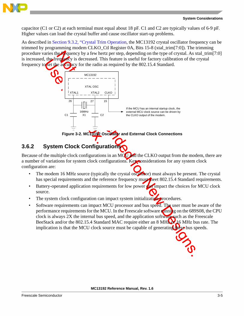
Not Recomm
ended for New Designs.
Use MC1320x.
System Considerations
MC13192 Reference Manual, Rev. 1.6
Freescale Semiconductor 3-5
capacitor (C1 or C2) at each terminal must equal about 18 pF. C1 and C2 are typically values of 6-9 pF. Higher values can load the crystal buffer and cause oscillator start-up problems.
As described in Section 9.3.2, “Crystal Trim Operation, the MC13192 crystal oscillator frequency can be trimmed by programming modem CLKO_Ctl Register 0A, Bits 15-8 (xtal_trim[7:0]). The trimming procedure varies the frequency by a few hertz per step, depending on the type of crystal. As xtal_trim[7:0] is increased, the frequency is decreased. This feature is useful for factory calibration of the crystal frequency to set the accuracy for the radio as required by the 802.15.4 Standard.
Figure 3-2. MC13192 Oscillator and External Clock Connections
3.6.2 System Clock ConfigurationsBecause of the multiple clock configurations in an MCU and the CLKO output from the modem, there are a number of variations for system clock configurations. Key considerations for any system clock configuration are:
• The modem 16 MHz source (typically the crystal oscillator) must always be present. The crystal has special requirements and the reference frequency must meet 802.15.4 Standard requirements.
• Battery-operated application requirements for low power can impact the choices for MCU clock source.
• The system clock configuration can impact system initialization procedures. • Software requirements can impact MCU processor and bus speed. The user must be aware of the
performance requirements for the MCU. In the Freescale software running on the 689S08, the CPU clock is always 2X the internal bus speed, and the application software such as the Freescale BeeStack and/or the 802.15.4 Standard MAC require either an 8 MHz or 16 MHz bus rate. The implication is that the MCU clock source must be capable of generating these bus speeds.
C1
XTAL OSC
XTAL1 XTAL2 CLKO
MC13192
26 27 15
16MHzX1 C2
If the MCU has an internal startup clock, the external MCU clock source can be driven by the CLKO output of the modem.

Not Recomm
ended for New Designs.
Use MC1320x.
MC13192 Reference Manual, Rev. 1.6
3-6 Freescale Semiconductor
System Considerations
3.6.3 Single System Crystal with CLKO driving MCU crystal inputThe single crystal (modem crystal) with CLKO driving the MCU external clock input is a common configuration for low cost and excellent frequency accuracy. The CLKO frequency is programmable from 16.393+ kHz to 16 Mhz and drives the MCU external source.
NOTEFor this system option to be usable, the system MCU must have an alternative (typically onboard) start-up clock.
In this configuration, clock start-up from a reset condition involves:• MCU reset is released and MCU starts on an internal clock.• Initialization software must reset and then release reset to the modem (MCU still running on
start-up clock).• Wait for modem start-up interrupt request (approximately 10 - 25 msec). CLKO default is active
with a frequency of 32.786+ kHz.• Program CLKO to a different frequency (if desired).• Wait for the CLKO source to lock, and then switch MCU clock to external source.
Additional considerations for this mode of operation include:• If the modem is forced to the Off condition and CLKO is killed, there is a 10 - 25 msec wait for the
modem CLKO to start from the Off condition after RST is released.• If the MCU puts the modem into Doze mode, keeping the CLKO alive is a higher power, but
available option.• If an accurate period is required for longer time delays (such as a beacon period), keeping CLKO
alive for very long periods is an option, but would be a higher power option typically than using a separate crystal for the MCU.
3.7 GPIO CharacteristicsThe modem GPIO hardware consists of 7 signals total (GPIO1-GPIO7). Immediately after reset, all the GPIO pins are configured as high-impedance general-purpose inputs. There are no internal pullup devices on these pins.
NOTETo avoid extra current drain from floating input pins, the power up initialization routine in the application program should change the direction of unused pins to outputs (programmed low) so the pins do not float. Outputs programmed low is the preferred option for lowest power.
As described in Section 3.5.4, “Modem Status Signals, GPIO1 and GPIO2 can be programmed as special status signals. The alternate functionality of the GPIO1-GPIO2 are controlled by the applications program and use of these pins is described in Chapter 9, “Miscellaneous Functions.
Not Recomm
ended for New Designs.
Use MC1320x.
System Considerations
MC13192 Reference Manual, Rev. 1.6
Freescale Semiconductor 3-7
The functionality of the modem GPIO is controlled by programming of the modem SPI registers via the SPI interface. For information about controlling all these pins as general-purpose I/O pins, see Chapter 9, “Miscellaneous Functions.
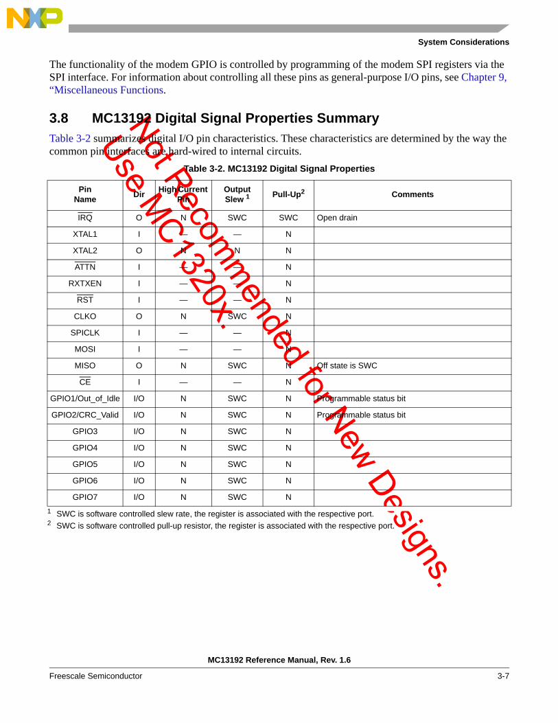
3.8 MC13192 Digital Signal Properties SummaryTable 3-2 summarizes digital I/O pin characteristics. These characteristics are determined by the way the common pin interfaces are hard-wired to internal circuits.
Table 3-2. MC13192 Digital Signal Properties
PinName Dir High Current
PinOutputSlew 1
1 SWC is software controlled slew rate, the register is associated with the respective port.
Pull-Up2
2 SWC is software controlled pull-up resistor, the register is associated with the respective port.
Comments
IRQ O N SWC SWC Open drain
XTAL1 I — — N
XTAL2 O N N N
ATTN I — — N
RXTXEN I — — N
RST I — — N
CLKO O N SWC N
SPICLK I — — N
MOSI I — — N
MISO O N SWC N Off state is SWC
CE I — — N
GPIO1/Out_of_Idle I/O N SWC N Programmable status bit
GPIO2/CRC_Valid I/O N SWC N Programmable status bit
GPIO3 I/O N SWC N
GPIO4 I/O N SWC N
GPIO5 I/O N SWC N
GPIO6 I/O N SWC N
GPIO7 I/O N SWC N

Not Recomm
ended for New Designs.
Use MC1320x.
MC13192 Reference Manual, Rev. 1.6
3-8 Freescale Semiconductor
System Considerations
3.9 Transceiver RF Port Operation and External ConnectionsThe MC13192 radio has features that allow for a flexible as well as low cost RF interface:
• Programmable output power - 0 dBm nominal output power, programmable from -27 dBm to +3 dBm typical
• <-92 dBm (typical) receive sensitivity - At 1% PER, 20-byte packet (well above 802.15.4 Standard of -85 dBm)
• A full differential set of RF RF_IN signals and a separate set of full differential PA outputs are provided. Separate inputs and outputs allow for a variety of RF configurations including external LNA and PA for increased range
• Onboard trim capability for 16 MHz crystal reference oscillator - The 802.15.4 Standard puts a +/- 40 ppm requirement on the carrier frequency. The onboard trim capability of the modem crystal oscillator eliminates need for external variable capacitors and allows for automated production frequency calibration. Also tighter tolerance can produce greater receive sensitivity
The RFIN+ and RFIN+ are receive inputs only, and PAO+ and PAO- are the differential PA output pins. These signals support a full differential dual port radio interface. Multiple external hardware configurations are possible.
Figure 3-3 shows two dual port configurations. First is a single antenna configuration with an external low noise amplifier (LNA) for greater range. An external antenna switch is used to multiplex the antenna between receive and transmit. An LNA is in the receive path to add gain for greater receive sensitivity. Two external baluns are required to convert the single-ended antenna switch signals to the differential signals required by the radio. An MCU GPIO signal is typically used to change direction of the antenna switch.
Figure 3-3 also shows a dual antenna configuration where there is a RX antenna and a TX antenna. For the receive side, the RX antenna is ac-coupled to the differential RFIN inputs and these capacitors along with inductor L1 form a matching network. Inductors L2 and L3 are ac-coupled to ground to form a frequency trap. For the transmit side, the TX antenna is connected to the differential PAO outputs, and inductors L4 and L5 provide DC-biasing to VDDA but are ac isolated. This dual antennae approach is a low cost option as the antennae can be printed wire devices.

Not Recomm
ended for New Designs.
Use MC1320x.
System Considerations
MC13192 Reference Manual, Rev. 1.6
Freescale Semiconductor 3-9
Figure 3-3. Dual Port RF Configuration Examples
3.10 Low Power ConsiderationsMany ZigBee and/or 802.15.4 Standard applications such as sensor End Devices are required to be battery operated. As expected, long battery life is highly desirable and is very dependent on application parameters. Over-the-air operation uses RX, TX, and CCA modes, where power is highest. As a result, the time between radio operations should be kept at the longest possible period that the application will allow.
When designing low power operation of the MC13192 consider:• The modem has several low power options.• The modem is entirely controlled by the MCU; the low power options/combinations will be
determined by MCU programming.
Using External Antenna Switch with LNA
Using Dual Antennae
Balun
Bypass
RFIN+
RFIN-
From MCUGPIO PAO+
PAO-
MC13192
LNAAntSw
Balun
VDD
VDDA
Bypass
L1
RFIN+
RFIN-
PAO+
PAO-
MC13192VDDA
TX Antenna
Bypass Bypass
L1
L2 L3
L4 L5
RX Antenna
Not Recomm
ended for New Designs.
Use MC1320x.
MC13192 Reference Manual, Rev. 1.6
3-10 Freescale Semiconductor
System Considerations
• The power down control of the modem must be maintained by the MCU in the MCU’s power down configuration.
Lowest power in a system is more than just putting the modem and/or the MCU in a low power mode. The relationship between the functions, the timing between them, and clock management must all be considered. The duty cycle between active operations is also very important as it can impact whether sleep operation or active operation will have the biggest impact over an extended time period.
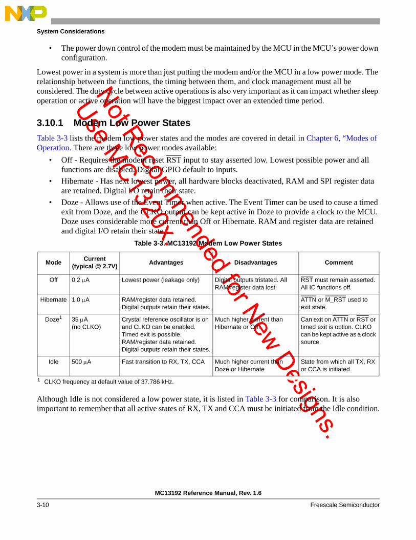
3.10.1 Modem Low Power StatesTable 3-3 lists the modem low power states and the modes are covered in detail in Chapter 6, “Modes of Operation. There are three low power modes available:
• Off - Requires the modem reset RST input to stay asserted low. Lowest possible power and all functions are disabled. Digital GPIO default to inputs.
• Hibernate - Has next lowest power, all hardware blocks deactivated, RAM and SPI register data are retained. Digital I/O retain their state.
• Doze - Allows use of the Event Timer when active. The Event Timer can be used to cause a timed exit from Doze, and the CLKO output can be kept active in Doze to provide a clock to the MCU. Doze uses considerable more current than Off or Hibernate. RAM and register data are retained and digital I/O retain their state.
Although Idle is not considered a low power state, it is listed in Table 3-3 for comparison. It is also important to remember that all active states of RX, TX and CCA must be initiated from the Idle condition.
Table 3-3. MC13192 Modem Low Power States
Mode Current(typical @ 2.7V) Advantages Disadvantages Comment
Off 0.2 μA Lowest power (leakage only) Digital outputs tristated. All RAM/register data lost.
RST must remain asserted. All IC functions off.
Hibernate 1.0 μA RAM/register data retained. Digital outputs retain their states.
ATTN or M_RST used to exit state.
Doze1
1 CLKO frequency at default value of 37.786 kHz.
35 μA(no CLKO)
Crystal reference oscillator is on and CLKO can be enabled. Timed exit is possible. RAM/register data retained. Digital outputs retain their states.
Much higher current than Hibernate or Off.
Can exit on ATTN or RST or timed exit is option. CLKO can be kept active as a clock source.
Idle 500 μA Fast transition to RX, TX, CCA Much higher current than Doze or Hibernate
State from which all TX, RX or CCA is initiated.

Not Recomm
ended for New Designs.
Use MC1320x.
System Considerations
MC13192 Reference Manual, Rev. 1.6
Freescale Semiconductor 3-11
3.10.2 Special Considerations for Hibernate and Doze Low Power ModesWhen using Hibernate or Doze mode, consideration must be given to the following issues.
3.10.2.1 Doze Current Higher Than SpecifiedThe Doze current (no CLKO output active) is specified as 35 µA (typical) on the data sheet with the programmed CLKO frequency at a default of 32.786 kHz. The Doze current can be considerably higher for certain combinations of higher CLKO frequencies and event timer prescale options. These combinations consist of:
1. CLKO frequency = 16 MHz with prescale select at 5, 6, or 7.2. CLKO frequency = 8 MHz with prescale select at 6, or 7.3. CLKO frequency = 4 MHz with prescale select at 7.
All other combinations have no problems. The higher current will not occur every time Doze is enabled. There is no potential harm either to the transceiver or its operation, the Doze current is simply higher.
To work around this issue, there are three choices:1. Accept higher current in Doze mode.2. Do not use any of the described combinations in Doze mode.3. If a higher CLKO frequency is desired when using CLKO as an MCU clock source, and the
desired prescale select can cause a problem, just before entering Doze mode, program the CLKO frequency to a lower value. Next, use the desired prescale value while in Doze. Finally, after exiting Doze mode, reprogram CLKO to the desired frequency before releasing the MCU clock to the CLKO source.
3.10.2.2 Asserting ATTN Early to Exit Hibernate or Doze ModeAsserting ATTN early can cause a problem if the transceiver has not fully entered Hibernate or Doze mode. Once the transceiver has been programmed to enter either Hibernate or Doze, the device does not fully enter the low power mode until 128 CLKO cycles have transpired. This is true whether or not the CLKO output is enabled. If the CLKO delay time is still active and ATTN is asserted, the IRQ for exiting the low power mode will be asserted, but reading the IRQ_Status register during the interrupt service routine will return no active bits. The status bit for exiting low power mode will not be set.
This situation can cause a problem with the interrupt service routine if the service routine does not return an interrupt source.
The delay time can vary from 128 clock cycles @ 16.393 kHz or ~7.8 msec to 128 clock cycles @ 16 MHz or 8 µsec. This is dependent on the selected CLKO frequency.
To work around this issue, there are three choices:1. Prevent the application from asserting ATTN during this period. As an example, for an End Node
that is sleeping for long periods, this would present no problems.

Not Recomm
ended for New Designs.
Use MC1320x.
MC13192 Reference Manual, Rev. 1.6
3-12 Freescale Semiconductor
System Considerations
2. If there is a potential for an early transceiver wake-up, program CLKO to a high frequency before entering Hibernate or Doze. The software can prevent an early wake-up within the short 8 µsec time. If this approach is used, Section 3.10.2.1, “Doze Current Higher Than Specified above must also be considered.
3. Write the application software knowing that an interrupt from exiting low power mode may not generate a valid status bit.
3.10.3 Recovery Times from Low Power ModesThe mode of operation is controlled by the MCU. The modem may be powered down if it is not in use while the MCU is doing another task or while the whole node is “sleeping”, i.e., the MCU is also powered down. Recovery time for both the modem and the MCU are important to system performance and the recovery times are independent of each other.
Each of the modem recovery times is from the low power condition to the Idle state. The start-up times for the Off and Hibernate conditions are considerably longer due to the start-up of the voltage regulators and clock oscillator. Figure 3-4 shows a simplified state diagram for the low power modes and gives the transition time to Idle:
• Off > Idle (10 - 25 ms) - The Off state is released by negating RST high. From that time until the modem asserts a ATTN interrupt and CLKO starts with a default frequency of 32.786+ kHz is 25 ms maximum.
• Hibernate > Idle (8 - 20 ms) - The Hibernate state is normally released via asserting ATTN low. The start-up time at 20 ms maximum is a little quicker than from the Off condition. The modem also asserts a ATTN interrupt (if enabled) and CLKO starts (if enabled) with the value programmed before entering Hibernate.
• Doze > Idle ((300 + 1/CLKO) μs) - The Doze state can be released via a timer or asserting ATTN low. The start-up time is considerably less ((300 + 1/CLKO) μs) because the clock oscillator is already running. CLKO can be programmed to run during Doze, and if not, CLKO will start if enabled for normal operation. An ATTN interrupt will be asserted (if enabled) when ATTN is used to exit Doze, or an interrupt will be asserted for exiting Doze Mode via a timer.
Figure 3-4. MC13192 Modem Low Power Recovery Times
OFF0.2µA
HIBERNATE1µA
DOZE35µA
IDLE500µA
10 - 25ms
8 - 20ms
(300+1/CLKO)ms

Not Recomm
ended for New Designs.
Use MC1320x.
System Considerations
MC13192 Reference Manual, Rev. 1.6
Freescale Semiconductor 3-13
3.10.3.1 Modem Active CurrentsIn normal operational mode the modem’s rest state in the Idle Mode. All active sequences originate from the Idle Mode and return to the Idle Mode. The three active sequences are Clear Channel Assessment (CCA), RX, and TX, and each has a separate current profile. Table 3-4 lists the typical currents while in the listed modes, but does not show the transition profiles when moving between modes.
A normal sequence of events may include an 802.15.4 Standard node performing first a CCA to see if the channel is clear, second transmitting a frame (assuming the channel is clear), and finally after the TX, going into to Receive Mode to look for an acknowledgement. The modem must be programmed for each of the operations separately and each operation has a different timing profile.
3.10.3.1.1 Modem CCA/ED Timing profile
The modem will scan for detected energy in a CCA operation (CCA is covered in detail in Section 6.3.5, “Clear Channel Assessment (CCA) Modes (including Link Quality Indication)). This is really a special case of RX so the CCA current is the same as RX. There are two versions of CCA where one is called CCA and the second is called Energy Detect (ED).
Figure 3-5 shows the timing profiles for both variations of a CCA operation. Once the CCA operation is initiated, the state machine moves through a warm-up period of 144 μs in which the analog regulators turn on and the analog RX circuitry comes to full power. The actual CCA or ED operation lasts 134 μs or 198 μs, respectively. During the warm-up period, the modem current is ramping from idle current (typically 500 μA) to full CCA current (typically 37 mA). The modem current for the CCA or ED is the full CCA current. After the CCA/ED operation times out, the return to idle current is very quick.
Figure 3-5. CCA and ED Timing Profiles
Table 3-4. MC13192 Active State Currents
Mode Current (typ @ 2.7V)
Idle 500 μA
CCA/ED 37 mA
RX 37 mA
TX(0 dBm nominal output power)
30 mA
WarmupIdle CCAState: Idle
WarmupIdle EDState: Idle
144 μs 134 μs
144 μs 198 μs

Not Recomm
ended for New Designs.
Use MC1320x.
MC13192 Reference Manual, Rev. 1.6
3-14 Freescale Semiconductor
System Considerations
3.10.3.1.2 Modem RX Timing profile
The receive or RX timing profile is very similar to the CCA profile. Figure 3-6 shows the timing profile for an RX operation. There is the initial 144 μs warm-up period from idle current to full RX current (typically 37 mA) followed by the RX operation (RX is covered in detail in Section 6.3, “Active Modes). The RX time is not a set figure as it is in a CCA operation. In some applications (typically not battery operated) such as a Coordinator, the receiver can be turned on for a majority of the time listening for End Devices or Routers. In an End Device (typically battery operated), the receiver can be typically turned on only when expecting an acknowledgement (ACK) of a transmission. The worst case RX on time can be when no ACK is received and the RX operation times out with not having received a frame.
The RX operation will end based on receiving the end of a frame or being terminated by the application having timed-out and aborted the RX operation. The return to Idle happens very quickly.
Figure 3-6. RX Timing Profile
3.10.3.1.3 Modem TX Timing profile
The transmit or TX timing profile is more predictable than the RX profile. Figure 3-7 shows the timing profile for a TX operation. There is the usual initial 144 μs warm-up period from idle current to full TX current (typically 30 mA) followed by the TX operation (TX is covered in detail in Section 6.3, “Active Modes). The TX time is not a set figure but it is predictable.
The raw transmission rate of the 802.15.4 Standard 2.4 GHz physical layer is 62.5 ksymbols/s or 250 kb/s. This means the TX time for 2 symbols or 1 byte of data is 32 μs. An 802.15.4 2.4 Standard compliant packet has 4 bytes of preamble, 1 byte of SFD, 1 byte of FLI, 2 bytes of FCS plus the payload data (125 bytes maximum). As a result the, the overhead of a frame is 8 bytes or 8 x 32 = 256 μs, and the maximum payload TX time is 125 x 32 = 4000 μs. The TX time for a packet then is:
Total TX time (μs) = 256 + (payload bytes x 32)
The TX operation will end after the FCS bytes are sent. The return to Idle has a “warm down” period of 10 μs to allow the RF transmitter to taper off in a manner to avoid RF “splatter”.
Figure 3-7. TX Timing Profile
WarmupIdle RXState: Idle
144 μs
WarmupIdle TXState: Idle
144 μs10 μs
Warm down

Not Recomm
ended for New Designs.
Use MC1320x.
System Considerations
MC13192 Reference Manual, Rev. 1.6
Freescale Semiconductor 3-15
3.10.4 General System Considerations for Low PowerLow power is most important for battery operated applications such as 802.15.4 Standard End Devices. In the modem the highest instantaneous power is dominated by the CCA, RX and TX modes. In the MCU, the current draw is typically dominated by the clock frequency. A number of general recommendations can help the user:
• Clock Management on the MCU— Use clock management as required to lower required power.— Run fast when the CPU performance is the critical path.— Run slow when waiting on peripherals (such as ATD conversion).— Be aware of software performance requirements (run time bus clock may need to be 16 MHz).— Use the external clock option for lowest power if possible (modem CLKO can supply
frequencies as high as 16 MHz).• The MCU can go to a lower power mode when the modem is recovering from the Off (10 - 25 ms)
or the Hibernate modes.• When the MCU is initializing from a “cold start” POR condition, the modem reset must be driven
to a low condition early in the routine. This is so the modem will start from a known condition and low power.
• Profile the use scenario of both the modem and the MCU when they are active. This is required to estimate current usage versus time and mode of operation.
• If possible, put the modem in a low power mode when the MCU is active and does not require interface with the modem. Doze can be useful to save power, provide CLKO, and be ready with a quick recovery time.
• Alternately put the MCU in a lower power mode if waiting on the modem IRQ.• Program all unused GPIO on both the modem and the MCU as outputs for lowest power.• The default condition is for MISO to go to tristate when CE is de-asserted. Program Control_B
Register 07, Bit 11, miso_hiz_en = 0 so MISO will be driven low when CE is de-asserted. As a result MISO will not float when Doze or Hibernate Mode is enabled.

Not Recomm
ended for New Designs.
Use MC1320x.
MC13192 Reference Manual, Rev. 1.6
3-16 Freescale Semiconductor
System Considerations
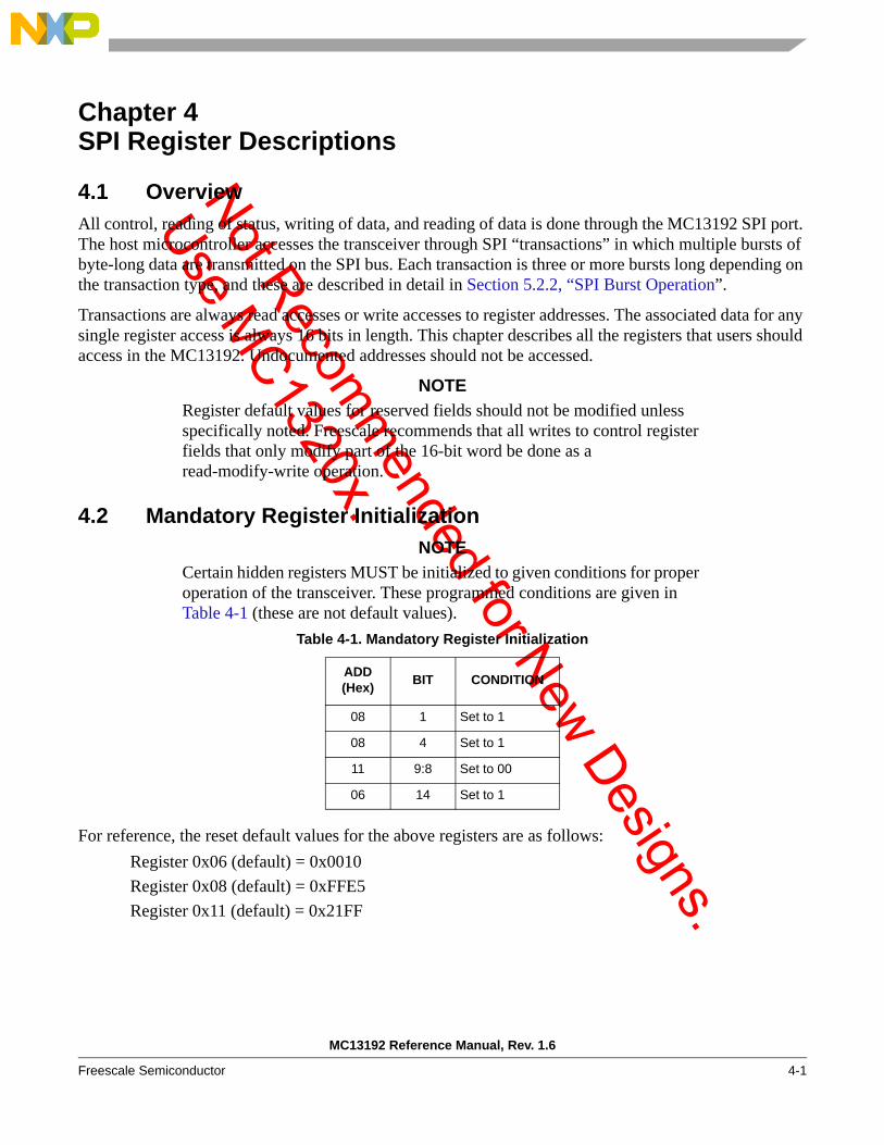
Not Recomm
ended for New Designs.
Use MC1320x.
MC13192 Reference Manual, Rev. 1.6
Freescale Semiconductor 4-1
Chapter 4 SPI Register Descriptions
4.1 OverviewAll control, reading of status, writing of data, and reading of data is done through the MC13192 SPI port. The host microcontroller accesses the transceiver through SPI “transactions” in which multiple bursts of byte-long data are transmitted on the SPI bus. Each transaction is three or more bursts long depending on the transaction type, and these are described in detail in Section 5.2.2, “SPI Burst Operation”.
Transactions are always read accesses or write accesses to register addresses. The associated data for any single register access is always 16 bits in length. This chapter describes all the registers that users should access in the MC13192. Undocumented addresses should not be accessed.
NOTERegister default values for reserved fields should not be modified unless specifically noted. Freescale recommends that all writes to control register fields that only modify part of the 16-bit word be done as a read-modify-write operation.
4.2 Mandatory Register InitializationNOTE
Certain hidden registers MUST be initialized to given conditions for proper operation of the transceiver. These programmed conditions are given in Table 4-1 (these are not default values).
For reference, the reset default values for the above registers are as follows:Register 0x06 (default) = 0x0010Register 0x08 (default) = 0xFFE5Register 0x11 (default) = 0x21FF
Table 4-1. Mandatory Register Initialization
ADD(Hex) BIT CONDITION
08 1 Set to 1
08 4 Set to 1
11 9:8 Set to 00
06 14 Set to 1

Not Recomm
ended for New Designs.
Use MC1320x.
MC13192 Reference Manual, Rev. 1.6
4-2 Freescale Semiconductor
SPI Register Descriptions
4.3 Register Model and Description DetailsTable 4-2 summarizes the MC13192 Register Model and the following sections describe each register in more detail.
Table 4-2. MC13192 SPI Register TableREGISTER
NAMEAdd(Hex) 15 14 13 12 11 10 9 8 7 6 5 4 3 2 1 0
Reset 00 software_reset
RX_Pkt_RAM 01 rx_pkt_ram[15:0]
TX_Pkt_RAM 02 tx_pkt_ram[15:0]
TX_Pkt_Ctl 03
tx_r
am2_
sele
ct
tx_pkt_length[6:0]
CCA_Thresh 04 cca_vt[7:0] power_comp[7:0]
IRQ_Mask 05
attn
_mas
k
ram
_add
r_m
ask
arb_
busy
_mas
k
strm
_dat
a_m
ask
pll_
lock
_mas
k
acom
a_en
doze
_mas
k
tmr4
_mas
k
tmr3
_mas
k
tmr2
_mas
k
tmr1
_mas
k
Control_A 06
tx_s
trm
rx_s
trm
cca_
mas
k
tx_s
ent_
mas
k
rx_r
cvd_
mas
k
tmr_
trig_
en
cca_
type
[1:0
]
xcvr
_seq
Control_B 07
tmr_
load
mis
o_hi
z_en
clko
_doz
e_en
tx_d
one_
mas
k
rx_d
one_
mas
k
use_
strm
_mod
e
hib_
en
doze
_en
PA_Enable 08
pa_e
n
Control_C 09
gpio
_alt_
en
clko
_en
tmr_
pres
cale
[2:0
]
CLKO_Ctl 0A xtal_trim[7:0] clko_rate[2:0]
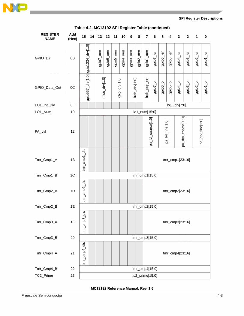
Not Recomm
ended for New Designs.
Use MC1320x.
SPI Register Descriptions
MC13192 Reference Manual, Rev. 1.6
Freescale Semiconductor 4-3
GPIO_Dir 0B
gpio
1234
_drv
[1:0
]
gpio
7_oe
n
gpio
6_oe
n
gpio
5_oe
n
gpio
4_oe
n
gpio
3_oe
n
gpio
2_oe
n
gpio
1_oe
n
gpio
7_ie
n
gpio
6_ie
n
gpio
5_ie
n
gpio
4_ie
n
gpio
3_ie
n
gpio
2_ie
n
gpio
1_ie
n
GPIO_Data_Out 0Cgp
io56
7_dr
v[1:
0]
mis
o_dr
v[1:
0]
clko
_drv
[1:0
]
irqb_
drv[
1:0]
irqb_
pup_
en
gpio
7_o
gpio
6_o
gpio
5_o
gpio
4_o
gpio
3_o
gpio
2_o
gpio
1_o
LO1_Int_Div 0F lo1_idiv[7:0]
LO1_Num 10 lo1_num[15:0]
PA_Lvl 12
pa_l
vl_c
oars
e[1:
0]
pa_l
vl_f
ine[
1:0]
pa_d
rv_c
oars
e[1:
0]
pa_d
rv_f
ine[
1:0]
Tmr_Cmp1_A 1B
tmr_
cmp1
_dis
tmr_cmp1[23:16]
Tmr_Cmp1_B 1C tmr_cmp1[15:0]
Tmr_Cmp2_A 1D
tmr_
cmp2
_dis
tmr_cmp2[23:16]
Tmr_Cmp2_B 1E tmr_cmp2[15:0]
Tmr_Cmp3_A 1F
tmr_
cmp3
_dis
tmr_cmp3[23:16]
Tmr_Cmp3_B 20 tmr_cmp3[15:0]
Tmr_Cmp4_A 21
tmr_
cmp4
_dis
tmr_cmp4[23:16]
Tmr_Cmp4_B 22 tmr_cmp4[15:0]
TC2_Prime 23 tc2_prime[15:0]
Table 4-2. MC13192 SPI Register Table (continued)REGISTER
NAMEAdd(Hex) 15 14 13 12 11 10 9 8 7 6 5 4 3 2 1 0
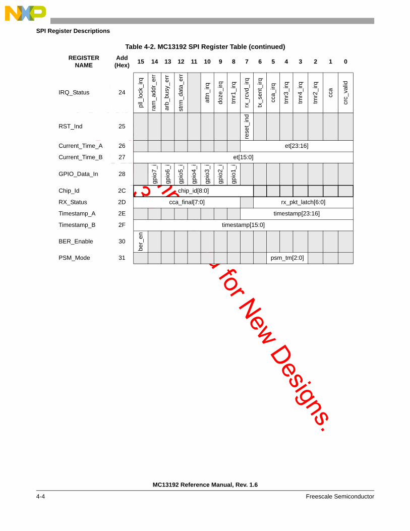
Not Recomm
ended for New Designs.
Use MC1320x.
MC13192 Reference Manual, Rev. 1.6
4-4 Freescale Semiconductor
SPI Register Descriptions
IRQ_Status 24
pll_
lock
_irq
ram
_add
r_er
r
arb_
busy
_err
strm
_dat
a_er
r
attn
_irq
doze
_irq
tmr1
_irq
rx_r
cvd_
irq
tx_s
ent_
irq
cca_
irq
tmr3
_irq
tmr4
_irq
tmr2
_irq
cca
crc_
valid
RST_Ind 25
rese
t_in
d
Current_Time_A 26 et[23:16]
Current_Time_B 27 et[15:0]
GPIO_Data_In 28
gpio
7_i
gpio
6_i
gpio
5_i
gpio
4_i
gpio
3_i
gpio
2_i
gpio
1_i
Chip_Id 2C chip_id[8:0]
RX_Status 2D cca_final[7:0] rx_pkt_latch[6:0]
Timestamp_A 2E timestamp[23:16]
Timestamp_B 2F timestamp[15:0]
BER_Enable 30
ber_
en
PSM_Mode 31 psm_tm[2:0]
Table 4-2. MC13192 SPI Register Table (continued)REGISTER
NAMEAdd(Hex) 15 14 13 12 11 10 9 8 7 6 5 4 3 2 1 0

Not Recomm
ended for New Designs.
Use MC1320x.
SPI Register Descriptions
MC13192 Reference Manual, Rev. 1.6
Freescale Semiconductor 4-5
4.4 Reset - Register 00Writing to Reset Register 00 causes a reset condition where the digital logic is reset, but the transceiver is not powered down. The device is forced to the Idle Mode and the SPI registers are all reset and forced to their default condition although all data in the Packet RAMs is retained. The reset is held as long as CE remains asserted and is released when CE is negated high. A read of this register has no effect.
4.5 RX_Pkt_RAM - Register 01The receive Packet RAM register is accessed when the MC13192 is being used in Packet Mode or Stream Mode for data transfer. In Packet Mode once a packet has been received, the payload data is stored in the RX Packet RAM and the length of the packet data is contained in Register 2D, Bit 6-0. A recursive read (see Section 5.5.1) to the RX_Pkt_RAM Register 01 is required to access the RX packet payload data.
In Stream Mode, the receive payload data is accessed word-by-word via repeated read accesses on the SPI bus. During Stream Mode when a valid data word is available in RX_Pkt_RAM, a rx_strm_irq status is set and an interrupt is generated (it must be enabled). Reading the RX_Pkt_RAM register will clear the rx_strm_irg interrupt so that reading the IRQ_Status Register 24 is not required (see Section 6.3.4.1).
Register 00 0x00
BIT 15 14 13 12 11 10 9 8 7 6 5 4 3 2 1 0
software_reset
TYPE w
RESET0 0 0 0 0 0 0 0 0 0 0 0 0 0 0 0
0x0000
Table 4-3. Register 00 Description
Name Description Operation
Bits 15-0 software_reset — Writing this register provides a software reset. When there is a SPI write to Register 00, the IC is reset and stays reset as long as CE remains asserted, and returns to normal operation when CE is negated. Read of this register has no effect.
Write data is “don’t care”
Register 01 0x01
BIT 15 14 13 12 11 10 9 8 7 6 5 4 3 2 1 0
rx_pkt_ram[15:0]
TYPE r/w
RESETx x x x x x x x x x x x x x x x
unknown from reset
Table 4-4. Register 01 Description
Name Description Operation
Bits 15-0 rx_pkt_ram[15:0] — These bits are the data channel for host access to the receive Packet RAM.
Default from RST reset is indeterminate.

Not Recomm
ended for New Designs.
Use MC1320x.
MC13192 Reference Manual, Rev. 1.6
4-6 Freescale Semiconductor
SPI Register Descriptions
4.6 TX_Pkt_RAM - Register 02The transmit Packet RAM register is accessed when the MC13192 is being used in Packet Mode or Stream Mode for data transfer. There are two transmit Packet RAMs and only one is accessed when the MC13192 is being used in Packet Mode for data transfer. In Packet Mode, the packet payload data must be written to the selected TX Packet RAM and the length of the packet data must be written to TX_Pkt_Ctl Register 03, Bits 6-0. A recursive write (see Section 5.5.2) to the TX_Pkt_RAM Register 02 is required to load the TX packet payload data.
In Stream Mode, the transmit payload data is written to Register 02 on a word-by-word basis via repeated accesses on the SPI bus. During Stream Mode when a data word is required for TX_Pkt_RAM, a tx_strm_irq status is set and an interrupt is generated (it must be enabled). Writing the TX_Pkt_RAM register will clear the tx_strm_irg interrupt so that reading the IRQ_Status Register 24 is not required (see Section 6.3.4.3).
Register 02 0x02
BIT 15 14 13 12 11 10 9 8 7 6 5 4 3 2 1 0
tx_pkt_ram[15:0]
TYPE r/w
RESETx x x x x x x x x x x x x x x x
unknown from reset
Table 4-5. Register 02 Description
Name Description Operation
Bits 15-0 tx_pkt_ram[15:0] — These bits are the data channel for host access to the selected transmit Packet RAM.
Default from reset is indeterminate.
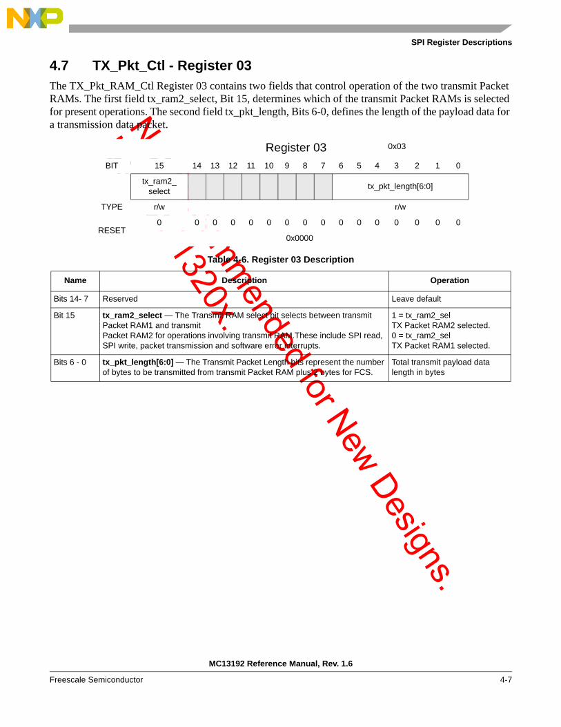
Not Recomm
ended for New Designs.
Use MC1320x.
SPI Register Descriptions
MC13192 Reference Manual, Rev. 1.6
Freescale Semiconductor 4-7
4.7 TX_Pkt_Ctl - Register 03The TX_Pkt_RAM_Ctl Register 03 contains two fields that control operation of the two transmit Packet RAMs. The first field tx_ram2_select, Bit 15, determines which of the transmit Packet RAMs is selected for present operations. The second field tx_pkt_length, Bits 6-0, defines the length of the payload data for a transmission data packet.
Register 03 0x03
BIT 15 14 13 12 11 10 9 8 7 6 5 4 3 2 1 0
tx_ram2_select tx_pkt_length[6:0]
TYPE r/w r/w
RESET0 0 0 0 0 0 0 0 0 0 0 0 0 0 0 0
0x0000
Table 4-6. Register 03 Description
Name Description Operation
Bits 14- 7 Reserved Leave default
Bit 15 tx_ram2_select — The Transmit RAM select bit selects between transmit Packet RAM1 and transmit Packet RAM2 for operations involving transmit RAM.These include SPI read, SPI write, packet transmission and software error interrupts.
1 = tx_ram2_sel TX Packet RAM2 selected.0 = tx_ram2_selTX Packet RAM1 selected.
Bits 6 - 0 tx_pkt_length[6:0] — The Transmit Packet Length bits represent the number of bytes to be transmitted from transmit Packet RAM plus 2 bytes for FCS.
Total transmit payload data length in bytes

Not Recomm
ended for New Designs.
Use MC1320x.
MC13192 Reference Manual, Rev. 1.6
4-8 Freescale Semiconductor
SPI Register Descriptions
4.8 CCA_Thresh - Register 04The CCA_Thresh Register 04 contains the cca_vt[7:0] 8-bit CCA threshold value, Bits 15 - 8. To calculate desired the cca_vt[7:0] value:
Threshold value = hex (| (Threshold Power in dBm) * 2 |)
A second field is power_comp[7:0], Bits 7 - 0, (default = 0x8D) which is an offset that is divided by 2 and added to the measured value of the average energy from a CCA/ED function or LQI value from an RX function, and the resulting value is stored in cca_final[7:0], RX_Status Register 2D. By using this power_comp[7:0] value, users can compensate the cca_final[7:0] value for external gain in the RX path. See Section 6.3.5.1 for more detailed information.
Register 04 0x04
BIT 15 14 13 12 11 10 9 8 7 6 5 4 3 2 1 0
cca_vt[7:0] power_comp[7:0]
TYPE r/w
RESET0 0 0 0 0 0 0 0 1 0 0 0 1 1 0 1
0x008D
Table 4-7. Register 04 Description
Name Description Operation
Bits 15-8 cca_vt[7:0] - Threshold value for Clear Channel Assessment in dB-linear format Default is 0x00.
Bits 7-0 power_comp[7:0] - This is a binary value that is added to the measured value of the CCA operation. The result is stored in cca_final[7:0]
Default is 0x8D

Not Recomm
ended for New Designs.
Use MC1320x.
SPI Register Descriptions
MC13192 Reference Manual, Rev. 1.6
Freescale Semiconductor 4-9
4.9 IRQ_Mask - Register 05The IRQ_Mask Register 05 provides most, but not all, mask bits for various interrupt sources for the MC13192. If a mask bit is set, its associated status bit being true will generate an interrupt on the MC13192 IRQ pin. The interrupt is cleared when the status bit is read via a SPI transaction.
Register 05 0x05
BIT 15 14 13 12 11 10 9 8 7 6 5 4 3 2 1 0
attn
_mas
k
ram
_add
r_m
ask
arb_
busy
_mas
k
strm
_dat
a_m
ask
pll_
lock
_mas
k
acom
a_en
doze
_mas
k
tmr4
_mas
k
tmr3
_mas
k
tmr2
_mas
k
tmr1
_mas
k
TYPE r/w r/w r/w r/w r/w r/w r/w r/w r/w r/w r/w
RESET1 0 0 0 0 0 0 0 0 1 0 0 0 0 0 0
0x8040
Table 4-8. Register 05 Description
Name Description Operation
Bits 14-13, 7-5
Reserved Leave default
Bit 15 attn_mask — The attention interrupt mask bit controls the attn_irq interrupt on the IRQ pin. Default is for the interrupt to be enabled out of reset.
1 = Allows attn_irq to generate an interrupt on the IRQ pin.0 = When attn_irq status bit is set, IRQ pin is not asserted.
Bit 12 ram_addr_mask — The Packet RAM address error interrupt mask bit controls the ram_addr_err interrupt on the IRQ pin.
1 = Allows ram_addr_err to generate an interrupt on the IRQ.0 = When ram_addr_err status bit is set, IRQ pin is not asserted.
Bit 11 arb_busy_mask — The Packet RAM arbiter busy error interrupt mask bit controls the arb_busy_err interrupt on the IRQ pin.
1 = Allows arb_busy_err to generate an interrupt on the IRQ pin.0 = When arb_busy_err status bit is set, IRQ pin is not asserted.
Bit 10 strm_data_mask — The Stream Mode data error interrupt mask bit controls the strm_data_irq interrupt on the IRQ pin.
1 = Allows strm_data_err to generate an interrupt on the IRQ pin.0 = When strm_data_err status bit is set, IRQ pin is not asserted.
Bit 9 pll_lock_mask — The LO1 unlock detect mask bit controls the pll_lock_irq interrupt on the IRQ pin.
1 = Allows pll_lock_irq to generate an interrupt on the IRQ pin.0 = When pll_lock_irq status bit is set, IRQ pin is not asserted.

Not Recomm
ended for New Designs.
Use MC1320x.
MC13192 Reference Manual, Rev. 1.6
4-10 Freescale Semiconductor
SPI Register Descriptions
Bit 8 acoma_en — The Acoma Mode enable bit controls Doze Mode. Acoma is an enhanced power save mode within Doze.
1 = The MC13192 stays in Doze until ATTN asserted. Event Timer and Prescaler clocks disabled for additional current savings.0 = Normal operation. Doze is exited by TC2 match or ATTN assertion.
Bit 4 doze_mask — The Doze timer interrupt mask bit controls the doze_irq interrupt on the IRQ pin.
1 = Allows doze_irq to generate an interrupt on the IRQ pin.0 = When doze_irq status bit is set, IRQ pin is not asserted.
Bit 3 tmr4_mask — The Event Timer four interrupt mask bit controls the tmr4_irq interrupt on the IRQ pin.
1 = Allows tmr4_irq to generate an interrupt on the IRQ pin.0 = When tmr4_irq status bit is set, IRQ pin is not asserted.
Bit 2 tmr3_mask — The Event Timer three interrupt mask bit controls the tmr3_irq interrupt on the IRQ pin.
1 = Allows tmr3_irq to generate an interrupt on the IRQ pin.0 = When tmr3_irq status bit is set, IRQ pin is not asserted.
Bit 1 tmr2_mask — The Event Timer two interrupt mask bit controls the tmr2_irq interrupt on the IRQ pin.
1 = Allows tmr2_irq to generate an interrupt on the IRQ pin.0 = When tmr2_irq status bit is set, IRQ pin is not asserted.
Bit 0 tmr1_mask — The Event Timer one interrupt mask bit controls the tmr1_irq interrupt on the IRQ pin.
1 = Allows tmr1_irq to generate an interrupt on the IRQ pin.0 = When tmr1_irq status bit is set, IRQ pin is not asserted.
Table 4-8. Register 05 Description (continued)
Name Description Operation
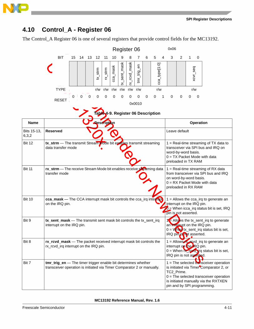
Not Recomm
ended for New Designs.
Use MC1320x.
SPI Register Descriptions
MC13192 Reference Manual, Rev. 1.6
Freescale Semiconductor 4-11
4.10 Control_A - Register 06The Control_A Register 06 is one of several registers that provide control fields for the MC13192.
Register 06 0x06
BIT 15 14 13 12 11 10 9 8 7 6 5 4 3 2 1 0
tx_s
trm
rx_s
trm
cca_
mas
k
tx_s
ent_
mas
k
rx_r
cvd_
mas
k
tmr_
trig_
en
cca_
type
[1:0
]
xcvr
_seq
TYPE r/w r/w r/w r/w r/w r/w r/w r/w
RESET0 0 0 0 0 0 0 0 0 0 0 1 0 0 0 0
0x0010
Table 4-9. Register 06 Description
Name Description Operation
Bits 15-13, 6,3,2
Reserved Leave default
Bit 12 tx_strm — The transmit Stream Mode bit enables transmit streaming data transfer mode
1 = Real-time streaming of TX data to transceiver via SPI bus and IRQ on word-by-word basis.0 = TX Packet Mode with data preloaded in TX RAM
Bit 11 rx_strm — The receive Stream Mode bit enables receive streaming data transfer mode
1 = Real-time streaming of RX data from transceiver via SPI bus and IRQ on word-by-word basis.0 = RX Packet Mode with data preloaded in RX RAM
Bit 10 cca_mask — The CCA interrupt mask bit controls the cca_irq interrupt on the IRQ pin.
1 = Allows the cca_irq to generate an interrupt on the IRQ pin.0 = When icca_irq status bit is set, IRQ pin is not asserted.
Bit 9 tx_sent_mask — The transmit sent mask bit controls the tx_sent_irq interrupt on the IRQ pin.
1 = Allows the tx_sent_irq to generate an interrupt on the IRQ pin.0 = When tx_sent_irq status bit is set, IRQ pin is not asserted.
Bit 8 rx_rcvd_mask — The packet received interrupt mask bit controls the rx_rcvd_irq interrupt on the IRQ pin.
1 = Allows rx_rcvd_irq to generate an interrupt on the IRQ pin.0 = When rx_rcvd_irq status bit is set, IRQ pin is not asserted.
Bit 7 tmr_trig_en — The timer trigger enable bit determines whether transceiver operation is initiated via Timer Comparator 2 or manually.
1 = The selected transceiver operation is initiated via Timer Comparator 2, or TC2_Prime.0 = The selected transceiver operation is initiated manually via the RXTXEN pin and by SPI programming.

Not Recomm
ended for New Designs.
Use MC1320x.
MC13192 Reference Manual, Rev. 1.6
4-12 Freescale Semiconductor
SPI Register Descriptions
Bits 5-4 cca_type[1:0] — The clear channel assessment type bits selects one of two possible CCA functions. Algorithm results are reported in field cca_final[7:0], RX_Status Register 2D, Bits 15 - 8.
01 = clear channel assessment10 = energy detection
Bits 1-0 xcvr_seq[1:0] — The transceiver operation bits select one of four possible transceiver modes.
00 = Idle (default)01 = CCA /energy detection10 = Packet Mode RX11 = Packet Mode TX
Table 4-9. Register 06 Description (continued)
Name Description Operation
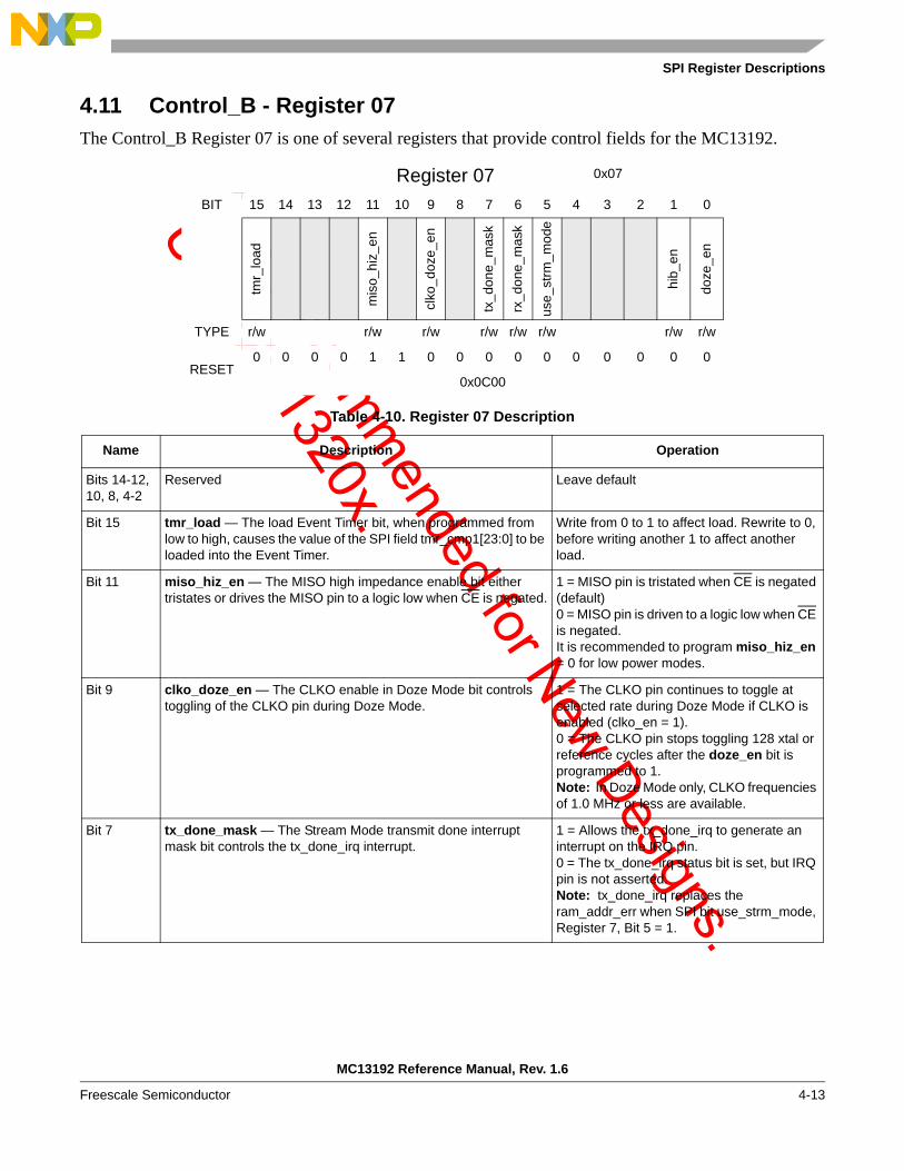
Not Recomm
ended for New Designs.
Use MC1320x.
SPI Register Descriptions
MC13192 Reference Manual, Rev. 1.6
Freescale Semiconductor 4-13
4.11 Control_B - Register 07The Control_B Register 07 is one of several registers that provide control fields for the MC13192.
Register 07 0x07
BIT 15 14 13 12 11 10 9 8 7 6 5 4 3 2 1 0
tmr_
load
mis
o_hi
z_en
clko
_doz
e_en
tx_d
one_
mas
k
rx_d
one_
mas
k
use_
strm
_mod
e
hib_
en
doze
_en
TYPE r/w r/w r/w r/w r/w r/w r/w r/w
RESET0 0 0 0 1 1 0 0 0 0 0 0 0 0 0 0
0x0C00
Table 4-10. Register 07 Description
Name Description Operation
Bits 14-12, 10, 8, 4-2
Reserved Leave default
Bit 15 tmr_load — The load Event Timer bit, when programmed from low to high, causes the value of the SPI field tmr_cmp1[23:0] to be loaded into the Event Timer.
Write from 0 to 1 to affect load. Rewrite to 0, before writing another 1 to affect another load.
Bit 11 miso_hiz_en — The MISO high impedance enable bit either tristates or drives the MISO pin to a logic low when CE is negated.
1 = MISO pin is tristated when CE is negated (default)0 = MISO pin is driven to a logic low when CE is negated.It is recommended to program miso_hiz_en = 0 for low power modes.
Bit 9 clko_doze_en — The CLKO enable in Doze Mode bit controls toggling of the CLKO pin during Doze Mode.
1 = The CLKO pin continues to toggle at selected rate during Doze Mode if CLKO is enabled (clko_en = 1).0 = The CLKO pin stops toggling 128 xtal or reference cycles after the doze_en bit is programmed to 1.Note: In Doze Mode only, CLKO frequencies of 1.0 MHz or less are available.
Bit 7 tx_done_mask — The Stream Mode transmit done interrupt mask bit controls the tx_done_irq interrupt.
1 = Allows the tx_done_irq to generate an interrupt on the IRQ pin. 0 = The tx_done_irq status bit is set, but IRQ pin is not asserted.Note: tx_done_irq replaces the ram_addr_err when SPI bit use_strm_mode, Register 7, Bit 5 = 1.

Not Recomm
ended for New Designs.
Use MC1320x.
MC13192 Reference Manual, Rev. 1.6
4-14 Freescale Semiconductor
SPI Register Descriptions
4.12 PA_Enable - Register 08The PA_Enable Register 08 contains the power amp (PA) enable bit which turns on and off the transmitter outputs. This feature is useful for sequences in RF test configurations. The default condition is with the transmitter enabled.
Bit 6 rx_done_mask — The Stream Mode receive done interrupt mask bit controls the rx_done_irq interrupt.
1 = Allows the rx_done_irq to generate an interrupt on the IRQ pin.0 = The rx_done_irq status bit is set, but IRQ pin is not asserted.Note: The rx_done_irq replaces the arb_busy_err when SPI bit use_strm_mode, Register 7, Bit 5 = 1.
Bit 5 use_strm_mode — The Stream Mode select bit selects Stream Mode or Packet Mode for transmit and receive data handling.
In Packet Mode, data is stored in RAM and handled as a packet. In Stream Mode, data is managed word-by-word through the SPI.0 = Packet Mode1 = Stream Mode
Bit 1 hib_en — The hibernate enable bit can set the MC13192 into its lowest power saving mode without a running time base.
1 = Places the MC13192 into its lowest power operating mode without a running time base. 0 = Normal operation.
Bit 0 doze_en — The doze enable bit can set the MC13192 into its lowest power saving mode with a running time base.
1 = Places the MC13192 into its lowest power operating mode with a running time base. 0 = Normal operation.
Register 08 0x08
BIT 15 14 13 12 11 10 9 8 7 6 5 4 3 2 1 0
pa_e
n
TYPE r/w
RESET1 1 1 1 1 1 1 1 1 1 1 0 0 1 0 1
0xFFE5
Table 4-11. Register 08 Description
Name Description Operation
Bits 14-0 Reserved
Bit 15 pa_en — The power amp (PA) enable bit controls the transmitter PA outputs.
1 = PA enabled.0 = PA disabled; the transmitter puts out no power.
Table 4-10. Register 07 Description (continued)
Name Description Operation

Not Recomm
ended for New Designs.
Use MC1320x.
SPI Register Descriptions
MC13192 Reference Manual, Rev. 1.6
Freescale Semiconductor 4-15
4.13 Control_C - Register 09The Control_C Register 09 is one of several registers that provide control fields for the MC13192.
Register 09 0x09
BIT 15 14 13 12 11 10 9 8 7 6 5 4 3 2 1 0
gpio
_alt_
en
clko
_en
tmr_
pres
cale
[2:0
]
TYPE r/w r/w r/w
RESET1 1 1 1 0 0 1 1 0 1 1 0 1 0 1 1
0xF36B
Table 4-12. Register 09 Description
Name Description Operation
Bits 15-8, 6, 4, 3
Reserved Leave default
Bit 7 gpio_alt_en — The GPIO alternative MCU interface enable bit controls GPIO1 and GPIO2.
1 = GPIO1 and GPIO2 are used as status to the MCU. GPIO1 indicates when the MC13192 is out of idle. GPIO2 indicates a valid CRC or CCA result. These signals are required for Freescale’s 802.15.4 Standard MAC software.0 = Normal GPIO operation.
Bit 5 clko_en — This bit enables the clock output which can be used as a reference clock for the MCU. Frequency is dependent on the value of clko_rate[2:0] (Register 0A, Bits 2 - 0).
1 = Output enabled (default).0 = Output low
Bits 2-0 tmr_prescale[2:0] — The Event Timer prescale value bits select the frequency of the base clock for the Event Timer module.
See Section 7.1 for more information.
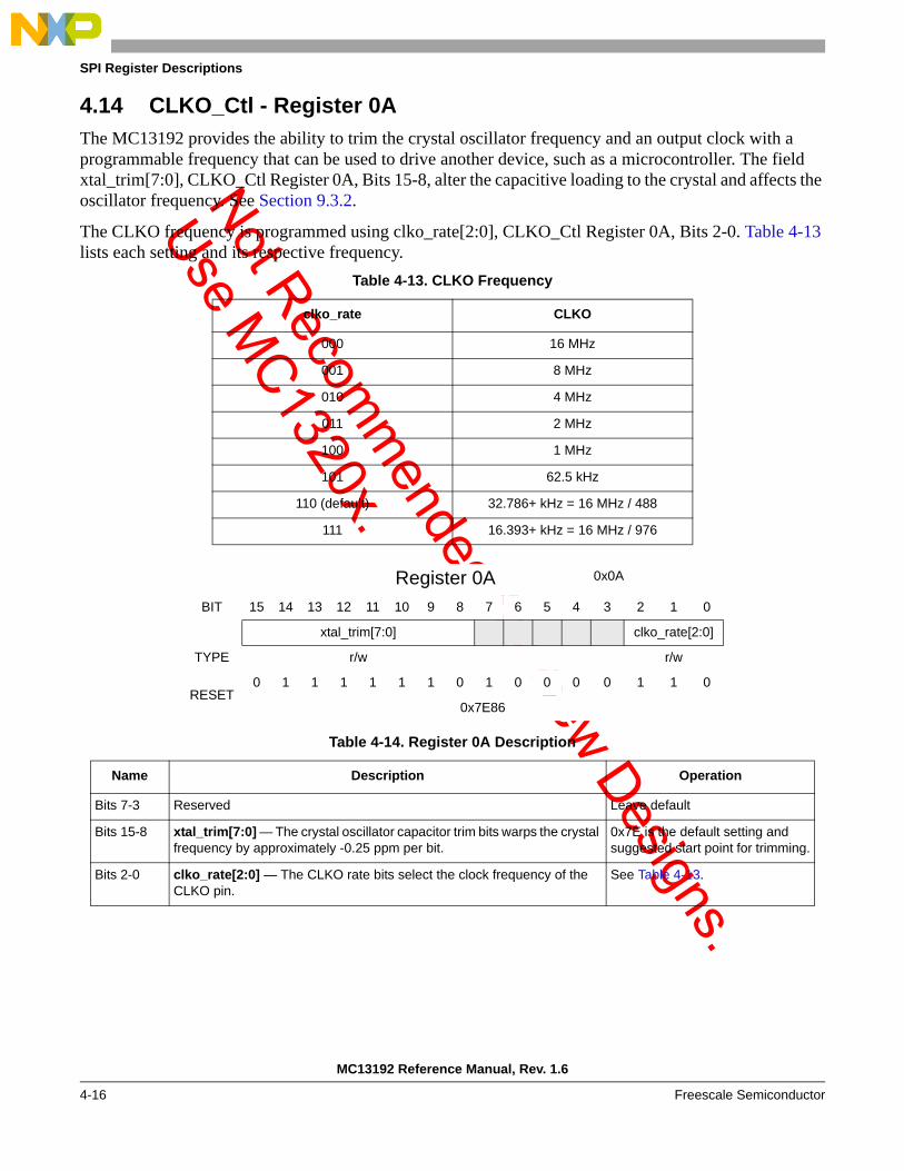
Not Recomm
ended for New Designs.
Use MC1320x.
MC13192 Reference Manual, Rev. 1.6
4-16 Freescale Semiconductor
SPI Register Descriptions
4.14 CLKO_Ctl - Register 0AThe MC13192 provides the ability to trim the crystal oscillator frequency and an output clock with a programmable frequency that can be used to drive another device, such as a microcontroller. The field xtal_trim[7:0], CLKO_Ctl Register 0A, Bits 15-8, alter the capacitive loading to the crystal and affects the oscillator frequency. See Section 9.3.2.
The CLKO frequency is programmed using clko_rate[2:0], CLKO_Ctl Register 0A, Bits 2-0. Table 4-13 lists each setting and its respective frequency.
Table 4-13. CLKO Frequency
clko_rate CLKO
000 16 MHz
001 8 MHz
010 4 MHz
011 2 MHz
100 1 MHz
101 62.5 kHz
110 (default) 32.786+ kHz = 16 MHz / 488
111 16.393+ kHz = 16 MHz / 976
Register 0A 0x0A
BIT 15 14 13 12 11 10 9 8 7 6 5 4 3 2 1 0
xtal_trim[7:0] clko_rate[2:0]
TYPE r/w r/w
RESET0 1 1 1 1 1 1 0 1 0 0 0 0 1 1 0
0x7E86
Table 4-14. Register 0A Description
Name Description Operation
Bits 7-3 Reserved Leave default
Bits 15-8 xtal_trim[7:0] — The crystal oscillator capacitor trim bits warps the crystal frequency by approximately -0.25 ppm per bit.
0x7E is the default setting and suggested start point for trimming.
Bits 2-0 clko_rate[2:0] — The CLKO rate bits select the clock frequency of the CLKO pin.
See Table 4-13.

Not Recomm
ended for New Designs.
Use MC1320x.
SPI Register Descriptions
MC13192 Reference Manual, Rev. 1.6
Freescale Semiconductor 4-17
4.15 GPIO_Dir - Register 0BThe GPIO_Dir Register 0B contains control bits for GPIO1 through GPIO7 that configure the data direction of each GPIO as well as a control field that sets the output drive strength of GPIO1 through GPIO4. Each GPIO bit has a corresponding bit to set the GPIO as an output and a separate corresponding bit to set the GPIO as an input. If both enable bits are set simultaneously for a given GPIO, the GPIO is configured as an input (input setting wins). During a hardware reset on RST, all the GPIO are tristated and the GPIO default to inputs.
Register 0B 0x0B
BIT 15 14 13 12 11 10 9 8 7 6 5 4 3 2 1 0
gpio
1234
_drv
[1:0
]
gpio
7_oe
n
gpio
6_oe
n
gpio
5_oe
n
gpio
4_oe
n
gpio
3_oe
n
gpio
2_oe
n
gpio
1_oe
n
gpio
7_ie
n
gpio
6_ie
n
gpio
5_ie
n
gpio
4_ie
n
gpio
3_ie
n
gpio
2_ie
n
gpio
1_ie
n
TYPE r/w r/w r/w r/w r/w r/w r/w r/w r/w r/w r/w r/w r/w r/w r/w
RESET0 0 0 0 0 0 0 0 0 1 1 1 1 1 1 1
0x007F
Table 4-15. Register 0B Description
Name Description Operation
Bits 15-14 gpio1234_drv[1:0]— These bits select output drive strength for GPIO1 through GPIO4.
00 (default) = lowest drive strength;11 = highest drive strength.
Bit 13 gpio7_oen— This bit configures GPIO7 as an output. 1 = GPIO7 enabled as output.0 = GPIO7 disabled as output.
Bit 12 gpio6_oen— This bit configures GPIO6 as an output. 1 = GPIO6 enabled as output.0 = GPIO6 disabled as output.
Bit 11 gpio5_oen— This bit configures GPIO5 as an output. 1 = GPIO5 enabled as output.0 = GPIO5 disabled as output.
Bit 10 gpio4_oen— This bit configures GPIO4 as an output. 1 = GPIO4 enabled as output.0 = GPIO4 disabled as output.
Bit 9 gpio3_oen— This bit configures GPIO3 as an output. 1 = GPIO3 enabled as output.0 = GPIO3 disabled as output.
Bit 8 gpio2_oen— This bit configures GPIO2 as an output. 1 = GPIO2 enabled as output.0 = GPIO2 disabled as output.
Bit 7 gpio1_oen— This bit configures GPIO1 as an output. 1 = GPIO1 enabled as output.0 = GPIO1 disabled as output.
Bit 6 gpio7_ien— This bit configures GPIO7 as an input. 1 = GPIO7 enabled as input.0 = GPIO7 disabled as input.
Bit 5 gpio6_ien— This bit configures GPIO6 as an input. 1 = GPIO6 enabled as input.0 = GPIO6 disabled as input.

Not Recomm
ended for New Designs.
Use MC1320x.
MC13192 Reference Manual, Rev. 1.6
4-18 Freescale Semiconductor
SPI Register Descriptions
Bit 4 gpio5_ien— This bit configures GPIO5 as an input. 1 = GPIO5 enabled as input.0 = GPIO5 disabled as input.
Bit 3 gpio4_ien— This bit configures GPIO4 as an input. 1 = GPIO4 enabled as input.0 = GPIO4 disabled as input.
Bit 2 gpio3_ien— This bit configures GPIO3 as an input. 1 = GPIO3 enabled as input.0 = GPIO3 disabled as input.
Bit 1 gpio2_ien— This bit configures GPIO2 as an input. 1 = GPIO2 enabled as input.0 = GPIO2 disabled as input.
Bit 0 gpio1_ien— This bit configures GPIO1 as an input. 1 = GPIO1 enabled as input.0 = GPIO1 disabled as input.
Table 4-15. Register 0B Description (continued)
Name Description Operation
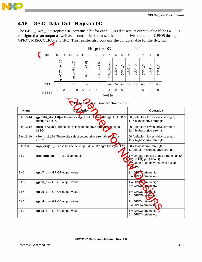
Not Recomm
ended for New Designs.
Use MC1320x.
SPI Register Descriptions
MC13192 Reference Manual, Rev. 1.6
Freescale Semiconductor 4-19
4.16 GPIO_Data_Out - Register 0CThe GPIO_Data_Out Register 0C contains a bit for each GPIO that sets its output value if the GPIO is configured as an output as well as a control fields that set the output drive strength of GPIO5 through GPIO7, MISO, CLKO, and IRQ. This register also contains the pullup enable for the IRQ pin.
Register 0C 0x0C
BIT 15 14 13 12 11 10 9 8 7 6 5 4 3 2 1 0
gpio
567_
drv[
1:0]
mis
o_dr
v[1:
0]
clko
_drv
[1:0
]
irqb_
drv[
1:0]
irqb_
pup_
en
gpio
7_o
gpio
6_o
gpio
5_o
gpio
4_o
gpio
3_o
gpio
2_o
gpio
1_o
TYPE r/w r/w r/w r/w r/w r/w r/w r/w r/w r/w r/w r/w
RESET0 0 0 0 0 0 1 1 1 0 0 0 0 0 0 0
0x0380
Table 4-16. Register 0C Description
Name Description Operation
Bits 15-14 gpio567_drv[1:0]— These bits select output drive strength for GPIO5 through GPIO7.
00 (default) = lowest drive strength;11 = highest drive strength.
Bits 13-12 miso_drv[1:0]- These bits select output drive strength for signal MISO.
00 (default) = lowest drive strength;11 = highest drive strength.
Bits 11-10 clko_drv[1:0]- These bits select output drive strength for signal CLKO.
00 (default) = lowest drive strength;11 = highest drive strength.
Bits 9-8 irqb_drv[1:0]- These bits select output drive strength for signal IRQ. 00 = lowest drive strength;11(default) = highest drive strength.
Bit 7 irqb_pup_en — IRQ pullup enable. 1 = Onboard pullup enabled (nominal 40 kΩ) on IRQ pin (default)0 = Open drain only (external pullup required).
Bit 6 gpio7_o — GPIO7 output value. 1 = GPIO7 driven high0 = GPIO7 driven low
Bit 5 gpio6_o — GPIO6 output value. 1 = GPIO6 driven high0 = GPIO6 driven low
Bit 4 gpio5_o — GPIO5 output value. 1 = GPIO5 driven high0 = GPIO5 driven low
Bit 3 gpio4_o — GPIO4 output value. 1 = GPIO4 driven high0 = GPIO4 driven low
Bit 2 gpio3_o — GPIO3 output value. 1 = GPIO3 driven high0 = GPIO3 driven low

Not Recomm
ended for New Designs.
Use MC1320x.
MC13192 Reference Manual, Rev. 1.6
4-20 Freescale Semiconductor
SPI Register Descriptions
4.17 LO1_Int_Div - Register 0FThe LO1_Int_Div Register 0F contains the 8-bit integer divide value for the LO1 fractional-N synthesizer that sets transceiver channel frequency. See Table 4-19.
Bit 1 gpio2_o — GPIO2 output value. 1 = GPIO2 driven high0 = GPIO2 driven low
Bit 0 gpio1_o — GPIO1 output value. 1 = GPIO1 driven high0 = GPIO1 driven low
Register 0F 0x0F
BIT 15 14 13 12 11 10 9 8 7 6 5 4 3 2 1 0
lo1_idiv[7:0]
TYPE r/w
RESET0 0 0 0 1 1 1 1 1 0 0 1 0 1 0 1
0x0F95
Table 4-17. Register 0F Description
Name Description Operation
Bits 15-8 Reserved. Leave default.
Bits 7-0 lo1_idiv[7:0] — The LO1 integer divide bits represent the integer divide value for the LO1 fractional-N synthesizer.
Default is 149dec (0x95). See Table 4-19.
Table 4-16. Register 0C Description (continued)
Name Description Operation

Not Recomm
ended for New Designs.
Use MC1320x.
SPI Register Descriptions
MC13192 Reference Manual, Rev. 1.6
Freescale Semiconductor 4-21
4.18 LO1_Num - Register 10The LO1_Num Register 10 contains the 16-bit integer numerator value for the LO1 fractional-N synthesizer that sets transceiver channel frequency. See Table 4-19.
Register 10 0x10
BIT 15 14 13 12 11 10 9 8 7 6 5 4 3 2 1 0
lo1_num[15:0]
TYPE r/w
RESET0 1 0 1 0 0 0 0 0 0 0 0 0 0 0 0
0x5000
Table 4-18. Register 10 Description
Name Description Operation
Bits 15-0 lo1_num[15:0] — These bits represent the numerator of the fractional divide value for the LO1 fractional-N synthesizer.
Default is 20,480dec (0x5000). See Table 4-19.
Table 4-19. Channel Operation
Channel
(Dec)
802.15.4ChannelNumber
Frequency
(MHz)
Integer Settinglo1_idiv[7:0](Dec / Hex)
Fractional Settinglo1_num[15:0]
(Dec / Hex)
1 11 2405 149 / 0x95 (default) 20480 / 0x5000 (default)
2 12 2410 149 / 0x95 40960 / 0xA000
3 13 2415 149 / 0x95 61440 / 0xF000
4 14 2420 150 / 0x96 16384 / 0x4000
5 15 2425 150 / 0x96 36864 / 0x9000
6 16 2430 150 / 0x96 57344 / 0xE000
7 17 2435 151 / 0x97 12288 / 0x3000
8 18 2440 151 / 0x97 32768 / 0x8000
9 19 2445 151 / 0x97 53248 / 0xD000
10 20 2450 152 / 0x98 8192 / 0x2000
11 21 2455 152 / 0x98 28672 / 0x7000
12 22 2460 152 / 0x98 49152 / 0xC000
13 23 2465 153 / 0x99 4096 / 0x1000
14 24 2470 153 / 0x99 24576 / 0x6000
15 25 2475 153 / 0x99 45056 / 0xB000
16 26 2480 154 / 0x9A 0 / 0x0000

Not Recomm
ended for New Designs.
Use MC1320x.
MC13192 Reference Manual, Rev. 1.6
4-22 Freescale Semiconductor
SPI Register Descriptions
4.19 PA_Lvl - Register 12The PA_Lvl Register 12 sets the power level and drive level of the transmitter power amplifier. See Table 6-3 for power level versus field settings.
Register 12 0x12
BIT 15 14 13 12 11 10 9 8 7 6 5 4 3 2 1 0
pa_l
vl_c
oars
e[1:
0]
pa_l
vl_f
ine[
1:0]
pa_d
rv_c
oars
e[1:
0]
pa_d
rv_f
ine[
1:0]
TYPE r/w r/w
RESET0 0 0 0 0 0 0 0 1 0 1 1 1 1 0 0
0x00BC
Table 4-20. Register 12 Description
Name Description Operation
Bits 15-8 Reserved Leave default
Bits 7-6 pa_lvl_coarse[1:0] - These bits select the coarse PA power level adjustment.
See Section 6.5 for more information.
Bits 5-4 pa_lvl_fine[1:0] - These bits selects fine PA power level adjustment. See Section 6.5 for more information.
Bits 3-2 pa_drv_coarse[1:0] - These bits select the coarse PA drive level adjustment.
Leave default
Bits 1-0 pa_drv_fine[1:0] - These bits select the fine PA drive level adjustment Leave default

Not Recomm
ended for New Designs.
Use MC1320x.
SPI Register Descriptions
MC13192 Reference Manual, Rev. 1.6
Freescale Semiconductor 4-23
4.20 Tmr_Cmp1_A - Register 1BThe Tmr_Cmp1_A Register 1B contains the disable bit for Timer Comparator 1 and stores the most significant 8 bits of the 24-bit compare value (the lower 16 bits of the compare value are stored in Tmr_CMP1_B Register 1C). With regard to using the timer comparator:
• It is suggested that the timer be disabled (writing tmr_cmp1_dis to 1) during system initialization as the default mode out of reset is timer enabled.
• The value in Register 1B will not be loaded in the comparator and the affect of the timer disable bit will not active until Register 1C is written. The 24-bit comparator value must be loaded into the comparator register in parallel, and as a result, the load is caused by a write Register 1C.
• Writing of Registers 1B and 1C can be done as a recursive SPI register write transaction or two separate singular transactions. Writing to Register 1C as a separate operation will always use the present value of Register 1B to load the comparator value and set the state of the disable bit.
4.21 Tmr_Cmp1_B - Register 1CThe Tmr_CMP1_B Register 1C stores the least significant 16 bits of the 24-bit compare value. Writing to Register 1C causes an internal load of the full 24-bit comparator value (see Section 4.20, “Tmr_Cmp1_A - Register 1B) and activates the mode presently set into the tmr_cmp1_dis control bit.
Register 1B 0x1B
BIT 15 14 13 12 11 10 9 8 7 6 5 4 3 2 1 0
tmr_
cmp1
_dis
tmr_cmp1[23:16]
TYPE r/w r/w
RESET0 0 0 0 0 0 0 0 1 1 1 1 1 1 1 1
0x00FF
Table 4-21. Register 1B Description
Name Description Operation
Bits 14-8 Reserved Leave default
Bit 15 tmr_cmp1_dis — This bit disables the Event Timer Comparator 1 function. 1 = Disables the Event Timer Compare 1 function.0 = Enables the Event Timer Compare 1 function (default).
Bits 7-0 tmr_cmp1[23:16] — These bits represent the 8 most significant bits of 24-bit Event Timer 1 absolute time compare value, tmr_cmp1[23:0].
Default is 0xFF.

Not Recomm
ended for New Designs.
Use MC1320x.
MC13192 Reference Manual, Rev. 1.6
4-24 Freescale Semiconductor
SPI Register Descriptions
Register 1C 0x1C
BIT 15 14 13 12 11 10 9 8 7 6 5 4 3 2 1 0
tmr_cmp1[15:0]
TYPE r/w
RESET1 1 1 1 1 1 1 1 1 1 1 1 1 1 1 1
0xFFFF
Table 4-22. Register 1C Description
Name Description Operation
Bits 15-0 tmr_cmp1[15:0] — These bits represent the 16 least significant bits of 24-bit Event Timer 1 absolute time compare value, tmr_cmp1[23:0].
Default is 0xFFFF.

Not Recomm
ended for New Designs.
Use MC1320x.
SPI Register Descriptions
MC13192 Reference Manual, Rev. 1.6
Freescale Semiconductor 4-25
4.22 Tmr_Cmp2_A - Register 1DThe Tmr_Cmp2_A Register 1B contains the disable bit for Timer Comparator 2 and stores the most significant 8 bits of the 24-bit compare value (the lower 16 bits of the compare value are stored in Tmr_CMP2_B Register 1E). With regard to using the timer comparator:
• It is suggested that the timer be disabled (writing tmr_cmp2_dis to 1) during system initialization as the default mode out of reset is timer enabled.
• The value in Register 1D will not be loaded in the comparator and the affect of the timer disable bit will not active until Register 1E is written. The 24-bit comparator value must be loaded into the comparator register in parallel, and as a result, the load is caused by a write Register 1E.
• Writing of Registers 1D and 1E can be done as a recursive SPI register write transaction or two separate singular transactions. Writing to Register 1E as a separate operation will always use the present value of Register 1D to load the comparator value and set the state of the disable bit.
4.23 Tmr_Cmp2_B - Register 1EThe Tmr_CMP2_B Register 1E stores the least significant 16 bits of the 24-bit compare value. Writing to Register 1E causes an internal load of the full 24-bit comparator value (see Section 4.22, “Tmr_Cmp2_A - Register 1D) and activates the mode presently set into the tmr_cmp2_dis control bit.
Register 1D 0x1D
BIT 15 14 13 12 11 10 9 8 7 6 5 4 3 2 1 0
tmr_
cmp2
_dis
tmr_cmp2[23:16]
TYPE r/w r/w
RESET0 0 0 0 0 0 0 0 1 1 1 1 1 1 1 1
0x00FF
Table 4-23. Register 1D Description
Name Description Operation
Bits 14-8 Reserved Leave default
Bit 15 tmr_cmp2_dis — This bit disables the Event Timer Comparator 2. 1 = Disables the Event Timer Compare 2 function.0 = Enables the Event Timer Compare 2 function (default).
Bits 7-0 tmr_cmp2[23:16] — These bits represent the 8 most significant bits of 24-bit Event Timer 2 absolute time compare value, tmr_cmp2[23:0].
Default is 0xFF.

Not Recomm
ended for New Designs.
Use MC1320x.
MC13192 Reference Manual, Rev. 1.6
4-26 Freescale Semiconductor
SPI Register Descriptions
Register 1E 0x1E
BIT 15 14 13 12 11 10 9 8 7 6 5 4 3 2 1 0
tmr_cmp2[15:0]
TYPE r/w
RESET1 1 1 1 1 1 1 1 1 1 1 1 1 1 1 1
0xFFFF
Table 4-24. Register 1E Description
Name Description Operation
Bits 15-0 tmr_cmp2[15:0] — These bits represent the 16 least significant bits of 24-bit Event Timer 2 absolute time compare value, tmr_cmp2[23:0].
Default is 0xFFFF.

Not Recomm
ended for New Designs.
Use MC1320x.
SPI Register Descriptions
MC13192 Reference Manual, Rev. 1.6
Freescale Semiconductor 4-27
4.24 Tmr_Cmp3_A - Register 1FThe Tmr_Cmp3_A Register 1F contains the disable bit for Timer Comparator 3and stores the most significant 8 bits of the 24-bit compare value (the lower 16 bits of the compare value are stored in Tmr_CMP3_B Register 20). With regard to using the timer comparator:
• It is suggested that the timer be disabled (writing tmr_cmp3_dis to 1) during system initialization as the default mode out of reset is timer enabled.
• The value in Register 1F will not be loaded in the comparator and the affect of the timer disable bit will not active until Register 20 is written. The 24-bit comparator value must be loaded into the comparator register in parallel, and as a result, the load is caused by a write Register 20.
• Writing of Registers 1F and 20 can be done as a recursive SPI register write transaction or two separate singular transactions. Writing to Register 20 as a separate operation will always use the present value of Register 1F to load the comparator value and set the state of the disable bit.
4.25 Tmr_Cmp3_B - Register 20The Tmr_CMP3_B Register 20 stores the least significant 16 bits of the 24-bit compare value. Writing to Register 20 causes an internal load of the full 24-bit comparator value (see Section 4.24, “Tmr_Cmp3_A - Register 1F) and activates the mode presently set into the tmr_cmp3_dis control bit.
Register 1F 0x1F
BIT 15 14 13 12 11 10 9 8 7 6 5 4 3 2 1 0
tmr_
cmp3
_dis
tmr_cmp3[23:16]
TYPE r/w r/w
RESET0 0 0 0 0 0 0 0 1 1 1 1 1 1 1 1
0x00FF
Table 4-25. Register 1F Description
Name Description Operation
Bits 14-8 Reserved Leave default
Bit 15 tmr_cmp3_dis — This bit disables the Event Timer Comparator 3 interrupt and status bit.
1 = Disables Event Timer Compare 3 function.0 = Enables Event Timer Compare 3 function (default).
Bits 7-0 tmr_cmp3[23:16] — These bits represent the 8 most significant bits of 24-bit Event Timer 3 absolute time compare value, tmr_cmp3[23:0].
Default is 0xFF.
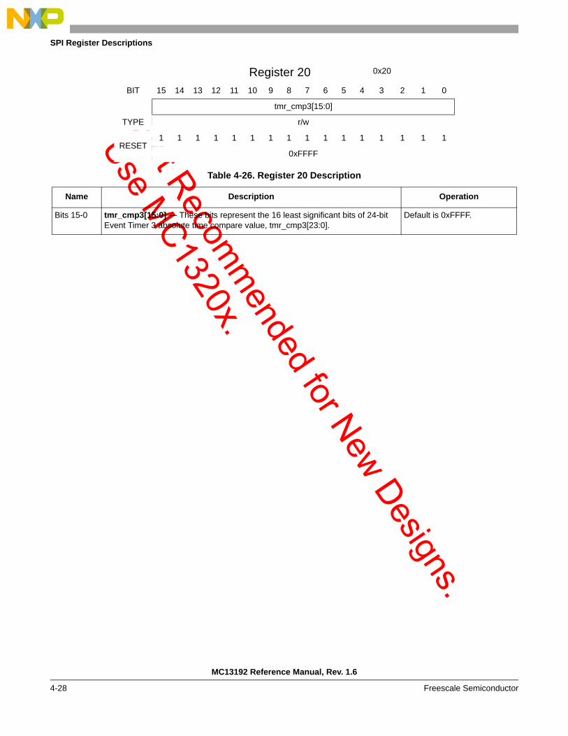
Not Recomm
ended for New Designs.
Use MC1320x.
MC13192 Reference Manual, Rev. 1.6
4-28 Freescale Semiconductor
SPI Register Descriptions
Register 20 0x20
BIT 15 14 13 12 11 10 9 8 7 6 5 4 3 2 1 0
tmr_cmp3[15:0]
TYPE r/w
RESET1 1 1 1 1 1 1 1 1 1 1 1 1 1 1 1
0xFFFF
Table 4-26. Register 20 Description
Name Description Operation
Bits 15-0 tmr_cmp3[15:0] — These bits represent the 16 least significant bits of 24-bit Event Timer 3 absolute time compare value, tmr_cmp3[23:0].
Default is 0xFFFF.

Not Recomm
ended for New Designs.
Use MC1320x.
SPI Register Descriptions
MC13192 Reference Manual, Rev. 1.6
Freescale Semiconductor 4-29
4.26 Tmr_Cmp4_A -Register 21The Tmr_Cmp4_A Register 21 contains the disable bit for Timer Comparator 4 and stores the most significant 8 bits of the 24-bit compare value (the lower 16 bits of the compare value are stored in Tmr_CMP4_B Register 22). With regard to using the timer comparator:
• It is suggested that the timer be disabled (writing tmr_cmp4_dis to 1) during system initialization as the default mode out of reset is timer enabled.
• The value in Register 21 will not be loaded in the comparator and the affect of the timer disable bit will not active until Register 22 is written. The 24-bit comparator value must be loaded into the comparator register in parallel, and as a result, the load is caused by a write Register 22.
• Writing of Registers 21 and 22 can be done as a recursive SPI register write transaction or two separate singular transactions. Writing to Register 22 as a separate operation will always use the present value of Register 21 to load the comparator value and set the state of the disable bit.
Register 21 0x21
BIT 15 14 13 12 11 10 9 8 7 6 5 4 3 2 1 0
tmr_
cmp4
_dis
tmr_cmp4[23:16]
TYPE r/w r/w
RESET0 0 0 0 0 0 0 0 1 1 1 1 1 1 1 1
0x00FF
Table 4-27. Register 21 Description
Name Description Operation
Bits 14-8 Reserved Leave default
Bit 15 tmr_cmp4_dis — This bit disables the Event Timer Comparator 4 interrupt and status bit.
1 = Disables Event Timer Compare 4 function.0 = Enables Event Timer Compare 4 function (default).
Bits 7-0 tmr_cmp4[23:16] — These bits represent the 8 most significant bits of 24-bit Event Timer 4 absolute time compare value, tmr_cmp4[23:0].
Default is 0xFF.

Not Recomm
ended for New Designs.
Use MC1320x.
MC13192 Reference Manual, Rev. 1.6
4-30 Freescale Semiconductor
SPI Register Descriptions
4.27 Tmr_Cmp4_B - Register 22The Tmr_CMP4_B Register 22 stores the least significant 16 bits of the 24-bit compare value. Writing to Register 22 causes an internal load of the full 24-bit comparator value (see Section 4.26, “Tmr_Cmp4_A -Register 21) and activates the mode presently set into the tmr_cmp4_dis control bit.
Register 22 0x22
BIT 15 14 13 12 11 10 9 8 7 6 5 4 3 2 1 0
tmr_cmp4[15:0]
TYPE r/w
RESET1 1 1 1 1 1 1 1 1 1 1 1 1 1 1 1
0xFFFF
Table 4-28. Register 22 Description
Name Description Operation
Bits 15-0 tmr_cmp4[15:0] — These bits represent the 16 least significant bits of 24-bit Event Timer 4 absolute time compare value, tmr_cmp4[23:0].
Default is 0xFFFF.

Not Recomm
ended for New Designs.
Use MC1320x.
SPI Register Descriptions
MC13192 Reference Manual, Rev. 1.6
Freescale Semiconductor 4-31
4.28 TC2_Prime - Register 23When the MC13192 is used in Stream Mode (Register 7, Bit 5 = 1), the 16-bit TC2_Prime Register 23 is used in place of the 24-bit Tmr_Cmp2 register(s) to initiate timer-triggered sequences. For an interrupt to be generated, tmr2_mask must be set (value = 1) and the interrupt is generated via the tmr2_irq status. Note that the tmr_cmp2_dis field should be disabled (value = 0) to use tc2_prime[15:0].
Register 23 0x23
BIT 15 14 13 12 11 10 9 8 7 6 5 4 3 2 1 0
tc2_prime[15:0]
TYPE r/w
RESET1 1 1 1 1 1 1 1 1 1 1 1 1 1 1 1
0xFFFF
Table 4-29. Register 23 Description
Name Description Operation
Bits 15-0 tc2_prime[15:0] — When use_strm_mode, Register 7, Bit 5 = 1, these bits are compared to the lower 16 bits of the Event Timer and initiate timer-triggered sequences when the value equal to current time.Note: tmr_trig_en, Register 6, Bit 7 must be set to 1. When use_strm_mode = 0, the TC2_Prime register is not used.
Default is 0xFFFF.

Not Recomm
ended for New Designs.
Use MC1320x.
MC13192 Reference Manual, Rev. 1.6
4-32 Freescale Semiconductor
SPI Register Descriptions
4.29 IRQ_Status - Register 24The IRQ_Status Register 24 contains status bits that can, in turn, cause an interrupt request when enabled. Reading the register clears the status bits and releases an associated interrupt request on IRQ. Note use of interrupt status Bit 14, Bit 13, Bit 7 and Bit 6 which are multiplexed and have special functionality.
Register 24 0x24
BIT 15 14 13 12 11 10 9 8 7 6 5 4 3 2 1 0pl
l_lo
ck_i
rq
ram
_add
r_er
r
arb_
busy
_err
strm
_dat
a_er
r
attn
_irq
doze
_irq
tmr1
_irq
rx_r
cvd_
irq
tx_s
ent_
irq
cca_
irq
tmr3
_irq
tmr4
_irq
tmr2
_irq
cca
crc_
valid
TYPE r r r r r r r r r r r r r r r r
RESET0 0 0 0 0 0 0 0 0 0 0 0 0 0 0 0
0x0000
Table 4-30. Register 24 Description
Name Description Operation
Bit 11 Reserved Leave default
Bit 15 pll_lock_irq — The Local Oscillator 1 Lock Detect Interrupt bit indicates whether the LO1 PLL is in or out of lock.
1 = LO1 PLL out of lock. Will cause an interrupt if pll_lock_mask is enabled.0 = LO1 PLL is locked.
Bit 14 ram_addr_err or tx_done_irq — The Packet RAM Address Error Interrupt or Stream Mode TX Done Interrupt bit is a multiplexed interrupt status bit.
When SPI bit use_strm_mode, Register 7, Bit 5 = 0, Register 24, Bit 14 represents ‘ram_addr_err’.ram_addr_err definition: a recursive SPI read or write operation to Packet RAM exceeded maximum RAM address.
When SPI bit use_strm_mode, Register 7, Bit 5 = 1, Register 24, Bit 14 represents ‘tx_done_irq’.tx_done_irq definition: TX Stream Mode reception complete and transceiver has returned to Idle.
Bit 13 arb_busy_err or rx_done_irq — The Packet RAM Arbiter Busy Error Interrupt or Steam Mode RX Done Interrupt bit is a multiplexed interrupt status bit.
When SPI bit use_strm_mode, Register 7, Bit 5 = 0, Register 24, Bit 13 represents ‘arb_busy_err’.arb_busy_err definition: a SPI read or write operation to Packet RAM attempted during packet reception or transmission, respectively.
When SPI bit use_strm_mode, Register 7, Bit 5 = 1, Register 24, Bit 13 represents ‘rx_done_irq’.rx_done_irq definition: RX Stream Mode reception complete and transceiver has returned to Idle Mode.
Bit 12 strm_data_err — The Stream Mode Data Error Interrupt bit indicates Stream Mode data read or write error
For RX Stream Mode, this bit gets set if a new RX word is updated to the SPI before the previous word is read.
For TX Stream Mode, the current TX word transmission is complete prior to next TX word being written to SPI.

Not Recomm
ended for New Designs.
Use MC1320x.
SPI Register Descriptions
MC13192 Reference Manual, Rev. 1.6
Freescale Semiconductor 4-33
Bit 10 attn_irq — The Attention Interrupt bit indicates the ATTN pin has been asserted or Power-up complete condition from a reset condition.
The bit being set indicates the ATTN signal has been asserted low or that the MC13192 has reached a Power-up complete condition after software reset (CE released) or a hardware reset (RST released).
Bit 9 doze_irq — The Doze Timer Interrupt bit. This bit gets set when the ‘tmr_cmp2[23:0]’ field matches the current Event Timer value while in Doze Mode. The MC13192 returns to Idle state from Doze Mode.
Bit 8 tmr1_irq — The Timer Compare 1 Interrupt bit. This bit gets set when the ‘tmr_cmp1[23:0]’ field matches the current Event Timer value.
Bit 7 rx_ rcvd_irq or rx_strm_irq — The RX Packet Received Interrupt or RX Stream Data Ready Interrupt bit is a multiplexed interrupt status bit
When SPI bit use_strm_mode, Register 7, Bit 5 = 0, Register 24, Bit 7 represents ‘rx_rcvd_irq’.rx_rcvd_irq definition: RX Packet Mode reception complete and transceiver has returned to Idle Mode.
When SPI bit use_strm_mode, Register 7, Bit 5 = 1, Register 24, Bit 7 represents ‘rx_strm_irq’.rx_strm_irq definition:1) First occurrence - RX Packet Length is available to be read.2) Subsequent occurrences - next receive Stream data word is ready to be read.
Bit 6 tx_ sent_irq or tx_strm_irq — The TX Packet Sent Interrupt or TX Stream Data Needed Interrupt bit is a multiplexed interrupt status bit.
When SPI bit use_strm_mode, Register 7, Bit 5 = 0, Register 24, Bit 6 represents ‘tx_sent_irq’.tx_sent_irq definition: TX Packet Mode operation complete and transceiver has returned to Idle Mode.
When SPI bit use_strm_mode, Register 7, Bit 5 = 1, Register 24, Bit 7 represents ‘tx_strm_irq’.tx_strm_irq definition: Transceiver is ready for next Stream transmit data word to be written.
Bit 5 cca_irq — The Clear Channel Assessment Ready Interrupt bit.
This bit is set when the ‘Clear Channel Assessment’ operation is complete.
Bit 4 tmr3_irq — The Timer Compare 3 Interrupt bit. This bit gets set when the ‘tmr_cmp3[23:0]’ field matches the current Event Timer value.
Bit 3 tmr4_irq — The Timer Compare 4 Interrupt bit. This bit gets set when the ‘tmr_cmp4[23:0]’ field matches the current Event Timer value.
Bit 2 tmr2_irq — The Timer Compare 2 Interrupt bit. This bit gets set when the ‘tmr_cmp2[23:0]’ field matches the current Event Timer value, or alternately if ‘tc2_prime[15:0]’ field matches the current Event Timer[15:0] when enabled.
Bit 1 cca — The Clear Channel Assessment bit indicates channel busy or channel idle.
1 = channel busy detected0 = channel idle detected
Note: For cca_type[1:0], Register 6, Bits 5:4 = 10, Energy Detect mode, CCA is not calculated and cca is held low.
Bit 0 crc_valid — The RX CRC Result bit denotes if the CRC is correct or not.
1 = RX CRC correct0 = RX CRC incorrect (default)
Table 4-30. Register 24 Description (continued)
Name Description Operation
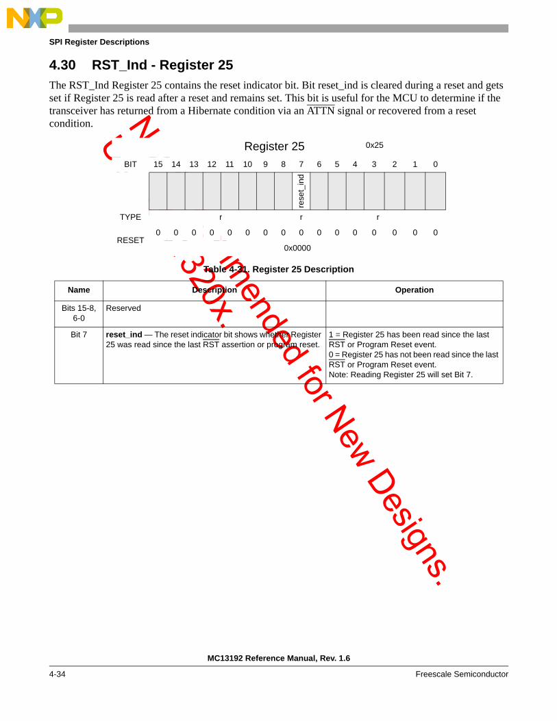
Not Recomm
ended for New Designs.
Use MC1320x.
MC13192 Reference Manual, Rev. 1.6
4-34 Freescale Semiconductor
SPI Register Descriptions
4.30 RST_Ind - Register 25The RST_Ind Register 25 contains the reset indicator bit. Bit reset_ind is cleared during a reset and gets set if Register 25 is read after a reset and remains set. This bit is useful for the MCU to determine if the transceiver has returned from a Hibernate condition via an ATTN signal or recovered from a reset condition.
Register 25 0x25
BIT 15 14 13 12 11 10 9 8 7 6 5 4 3 2 1 0
rese
t_in
d
TYPE r r r
RESET0 0 0 0 0 0 0 0 0 0 0 0 0 0 0 0
0x0000
Table 4-31. Register 25 Description
Name Description Operation
Bits 15-8, 6-0
Reserved
Bit 7 reset_ind — The reset indicator bit shows whether Register 25 was read since the last RST assertion or program reset.
1 = Register 25 has been read since the last RST or Program Reset event.0 = Register 25 has not been read since the last RST or Program Reset event.Note: Reading Register 25 will set Bit 7.

Not Recomm
ended for New Designs.
Use MC1320x.
SPI Register Descriptions
MC13192 Reference Manual, Rev. 1.6
Freescale Semiconductor 4-35
4.31 Current_Time_A - Register 26The Current_Time_A Register 26 is read to get the 8 most significant bits of the current value of the 24-bit counter of the Event Timer.
4.32 Current_Time_B - Register 27The Current_Time_B Register 27 is read to get the 16 least significant bits of the current value of the 24-bit counter of the Event Timer.
Register 26 0x26
BIT 15 14 13 12 11 10 9 8 7 6 5 4 3 2 1 0
et[23:16]
TYPE r
RESET0 0 0 0 0 0 0 0 0 0 0 0 0 0 0 0
0x0000
Table 4-32. Register 26 Description
Name Description Operation
Bits 15-8 Reserved
Bits 7 - 0 et [23:16]— These bits are the 8 most significant bits of the current time in the Event Timer counter.
Register 27 0x27
BIT 15 14 13 12 11 10 9 8 7 6 5 4 3 2 1 0
et[15:0]
TYPE r
RESET0 0 0 0 0 0 0 0 0 0 0 0 0 0 0 0
0x0000
Table 4-33. Register 27 Description
Name Description Operation
Bits 15-0 et[15:0] — These bits represent the 16 least significant bits of the current time of the Event Timer counter.

Not Recomm
ended for New Designs.
Use MC1320x.
MC13192 Reference Manual, Rev. 1.6
4-36 Freescale Semiconductor
SPI Register Descriptions
4.33 GPIO_Data_In - Register 28The GPIO_Data_In Register 28 is read to determine the state of any GPIO that are configured as an input.
Register 28 0x28
BIT 15 14 13 12 11 10 9 8 7 6 5 4 3 2 1 0
gpio
7_i
gpio
6_i
gpio
5_i
gpio
4_i
gpio
3_i
gpio
2_i
gpio
1_i
TYPE r r r r r r r
RESETx x x x x x x
Unknown from reset
Table 4-34. Register 28 Description
Name Description Operation
Bits 15, 7-0 Reserved
Bit 14 gpio7_i — This bit is the input value of GPIO7. With gpio7_oen = 0 and gpio7_ien = 1; GPIO7 is configured as an input whose value can be read from gpio7_i.
Bit 13 gpio6_i — This bit is the input value of GPIO6. With gpio6_oen = 0 and gpio6_ien = 1; GPIO6 is configured as an input whose value can be read from gpio6_i.
Bit 12 gpio5_i — This bit is the input value of GPIO5. With gpio5_oen = 0 and gpio5_ien = 1; GPIO5 is configured as an input whose value can be read from gpio5_i.
Bit 11 gpio4_i — This bit is the input value of GPIO4. With gpio4_oen = 0 and gpio4_ien = 1; GPIO4 is configured as an input whose value can be read from gpio4_i.
Bit 10 gpio3_i — This bit is the input value of GPIO3. With gpio3_oen = 0 and gpio3_ien = 1; GPIO3 is configured as an input whose value can be read from gpio3_i.
Bit 9 gpio2_i — This bit is the input value of GPIO2. With gpio2_oen = 0 and gpio2_ien = 1; GPIO2 is configured as an input whose value can be read from gpio2_i.
Bit 8 gpio1_i — This bit is the input value of GPIO1. With gpio1_oen = 0 and gpio1_ien = 1; GPIO1 is configured as an input whose value can be read from gpio1_i.

Not Recomm
ended for New Designs.
Use MC1320x.
SPI Register Descriptions
MC13192 Reference Manual, Rev. 1.6
Freescale Semiconductor 4-37
4.34 Chip_ID - Register 2CThe Chip_ID Register 2C is read to get the 9-bit chip version code contained in the chip_id[8:0] field. The present version numbers include 0x5000 and 0x5400. Version 0x5400 is the latest version of the device.
4.35 RX_Status - Register 2DThe RX_Status Register 2D has two fields, the first of which represents the average results of the CCA algorithm selected by cca_type[1:0], Register 6, Bits 5-4. The second field gives the receive packet length parsed from the packet header; the value is latched after an RX Start Frame Delimiter is detected.
During a RX Stream Mode sequence, loading a valid FLI in rx_pkt_latch[6:0] causes the first rx_strm_irq status and interrupt in the sequence. Reading RX_Status Register 2D for that first rx_strm_irq interrupt will clear the status and the interrupt. As a result, reading IRQ_Status Register 24 is not required (see Section 6.3.4.1).
Register 2C 0x2C
BIT 15 14 13 12 11 10 9 8 7 6 5 4 3 2 1 0
chip_id[8:0]
TYPE r
RESET0 1 0 1 0 0 0 0 0 0 0 0 0 0 0 0
0x5000 or 0x5400
Table 4-35. Register 2C Description
Name Description Operation
Bits 6-0 Reserved
Bits 15- 7 chip_id [8:0]— These bits are the 9-bit chip version code for the transceiver. Version dependent.
Register 2D 0x2D
BIT 15 14 13 12 11 10 9 8 7 6 5 4 3 2 1 0
cca_final[7:0] rx_pkt_latch[6:0]
TYPE r r
RESET0 0 0 0 0 0 0 0 0 0 0 0 0 0 0 0
0x0000
Table 4-36. Register 2D Description
Name Description Operation
Bit 7 Reserved
Bits 15-8 cca_final [7:0] — Average CCA energy. These bits represent the average result of the CCA algorithm selected by cca_type[1:0], Register 6, Bits 5-4.
Bits 6- 0 rx_pkt_latch [6:0] — RX packet length These bits give the RX packet length parsed from the packet header. The value is latched when an RX Start Frame Delimiter is detected.

Not Recomm
ended for New Designs.
Use MC1320x.
MC13192 Reference Manual, Rev. 1.6
4-38 Freescale Semiconductor
SPI Register Descriptions
4.36 Timestamp_A - Register 2EThe Timestamp_A Register 2E stores the most significant 8 bits of the value in the Event Timer counter (et[23:0]) when the beginning of the most recent receive packet occurred. The value is latched immediately following reception of the FLI field and at the beginning of the payload data.
4.37 Timestamp_B - Register 2FThe Timestamp_B Register 2F stores the least significant 16 bits of the value in the Event Timer counter (et[23:0]) when the beginning of the most recent receive packet occurred. The value is latched immediately following reception of the FLI field and at the beginning of the payload data.
Register 2E 0x2E
BIT 15 14 13 12 11 10 9 8 7 6 5 4 3 2 1 0
timestamp[23:16]
TYPE r
RESET0 0 0 0 0 0 0 0 0 0 0 0 0 0 0 0
0x0000
Table 4-37. Register 2E Description
Name Description Operation
Bits 15-8 Reserved
Bits 7 - 0 timestamp [23:16]— 8 most significant bits of the latched 24-bit timestamp value for the beginning of the receive packet.
Register 2F 0x2F
BIT 15 14 13 12 11 10 9 8 7 6 5 4 3 2 1 0
timestamp[15:0]
TYPE r
RESET0 0 0 0 0 0 0 0 0 0 0 0 0 0 0 0
0x0000
Table 4-38. Register 2F Description
Name Description Operation
Bits 15-0 timestamp[15:0] — 16 least significant bits of the latched 24-bit timestamp value for the beginning of the receive packet.

Not Recomm
ended for New Designs.
Use MC1320x.
SPI Register Descriptions
MC13192 Reference Manual, Rev. 1.6
Freescale Semiconductor 4-39
4.38 BER_Enable - Register 30The BER_Enable Register 30 contains the bit error rate test enable bit which allows the transceiver to be put into continuous receive or transmit mode. This feature has useful sequences in RF test configurations (see application note AN2976, MC1319x RF Test Modes). The default condition is with the continuous mode disabled.
Register 30 0x30
BIT 15 14 13 12 11 10 9 8 7 6 5 4 3 2 1 0be
r_en
TYPE r/w
RESET0 0 0 0 0 0 0 0 0 0 0 0 0 1 0 0
0x0004
Table 4-39. Register 30 Description
Name Description Operation
Bits 14-0 Reserved
Bit 15 ber_en — The bit error rate test enable bit allows the transceiver to be put into continuous receive or transmit mode. Continuous TX Mode is useful for current measurements or for looking at TX spectrum. Continuous RX Mode is useful for looking at current.
1 = When a TX operation or RX operation is enabled, the transceiver stays in that operation until aborted.0 = Continuous operation disabled; normal operation.
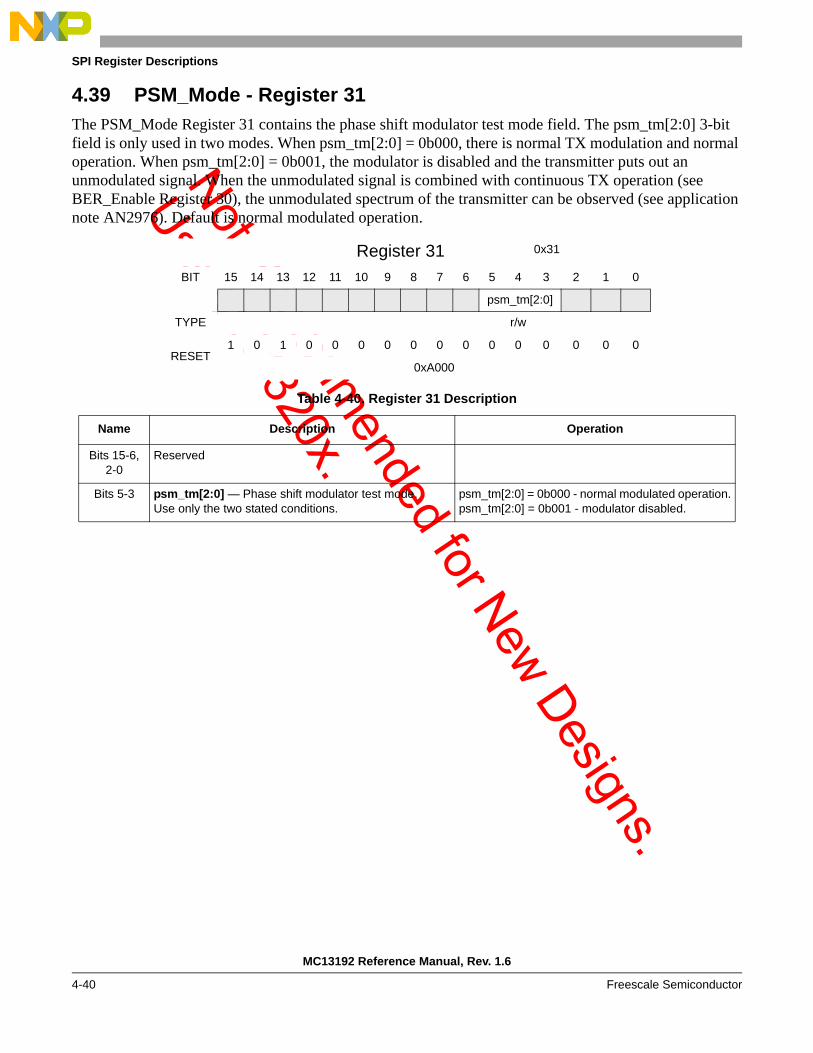
Not Recomm
ended for New Designs.
Use MC1320x.
MC13192 Reference Manual, Rev. 1.6
4-40 Freescale Semiconductor
SPI Register Descriptions
4.39 PSM_Mode - Register 31The PSM_Mode Register 31 contains the phase shift modulator test mode field. The psm_tm[2:0] 3-bit field is only used in two modes. When psm_tm[2:0] = 0b000, there is normal TX modulation and normal operation. When psm_tm[2:0] = 0b001, the modulator is disabled and the transmitter puts out an unmodulated signal. When the unmodulated signal is combined with continuous TX operation (see BER_Enable Register 30), the unmodulated spectrum of the transmitter can be observed (see application note AN2976). Default is normal modulated operation.
Register 31 0x31
BIT 15 14 13 12 11 10 9 8 7 6 5 4 3 2 1 0
psm_tm[2:0]
TYPE r/w
RESET1 0 1 0 0 0 0 0 0 0 0 0 0 0 0 0
0xA000
Table 4-40. Register 31 Description
Name Description Operation
Bits 15-6, 2-0
Reserved
Bits 5-3 psm_tm[2:0] — Phase shift modulator test mode. Use only the two stated conditions.
psm_tm[2:0] = 0b000 - normal modulated operation.psm_tm[2:0] = 0b001 - modulator disabled.

Not Recomm
ended for New Designs.
Use MC1320x.
MC13192 Reference Manual, Rev. 1.6
Freescale Semiconductor 5-1
Chapter 5 Serial Peripheral Interface (SPI)
5.1 OverviewControl of the MC13192 and data transfers are accomplished by means of a 4-wire Serial Peripheral Interface (SPI). The SPI port is a fully static design that requires no additional clocks besides SPICLK for accessing internal registers, although Packet RAM accesses do require the reference oscillator to be running. This allows for lower power when the SPI must stay alive while the rest of the device is in power-down.
Although the normal SPI protocol is based on 8-bit transfers, the MC13192 imposes a higher level transaction protocol that is based on multiple 8-bit transfers per transaction. In its simplest form, a singular SPI read or write transaction consists of an 8-bit header transfer followed by two 8-bit data transfers. The header denotes access type and register address. The following bytes are read or write data. The SPI also supports recursive ‘data burst’ transactions in which additional data transfers can occur. The recursive mode is primarily intended for Packet RAM access and fast configuration of the MC13192. Partial word accesses are not supported.
All SPI accessible registers are configured with 16-bit data width. The address range is 6 bits which allows for 64 locations although not all are implemented. Internal data RAMs are accessed as dedicated addresses within the register address field.
An additional feature is a software reset capability where a write to Address 00 will accomplish most of the equivalency of a hardware reset.
5.2 SPI Basic OperationThe MC13192 operates as a SPI Slave only. The host microcontroller supplies the interface clock and acts as SPI master.
5.2.1 SPI Pin DefinitionThe MC13912 SPI signals of CE, CPICLK, MOSI, and MISO are defined in the following paragraphs. A typical interconnection to a microcontroller is shown in Figure 5-1.
Figure 5-1. Typical SPI Connection with an MCU.
Shift Register
Baud RateGenerator
Shift Register
Chip Enable (CE)
RxD MISO
TxD MOSI
Sclk SPICLK
MCU MC13192
CE

Not Recomm
ended for New Designs.
Use MC1320x.
MC13192 Reference Manual, Rev. 1.6
5-2 Freescale Semiconductor
Serial Peripheral Interface (SPI)
5.2.1.1 Chip Enable (CE)A transaction on the SPI port is framed by the active low Chip Enable (CE) input signal which is driven by the host MCU. A transaction is a minimum of 3 SPI bursts and can extend to a greater number of bursts.
5.2.1.2 SPI Clock (SPICLK)The host drives the SPI Clock (SPICLK) input to the MC13192. Data is clocked into the master or slave on the leading (rising) edge of the return-to-zero SPICLK and data out changes state on the trailing (falling) edge of SPICLK.
NOTEFor Freescale microcontrollers, the SPI clock format is the clock phase control bit CPHA = 0 and the clock polarity control bit CPOL = 0.
5.2.1.3 Master Out / Slave In (MOSI)The Master Out/Slave In (MOSI) input presents incoming data from the host to the transceiver (slave input).
5.2.1.4 Master In / Slave Out (MISO)The MC13192 presents data to the master on its MISO output. This output is user configurable for both drive strength and its off state.
5.2.1.4.1 Setting MISO Output Drive Strength
MISO output drive strength is programmed by writing to miso_drv[1:0], GPIO_Data_Out Register 0C. There are 4 levels of drive strength with field value 00 for lowest and value 11 for greatest. The default value is 00.
NOTEIt is suggested the user program MISO for greatest drive strength for best performance.
5.2.1.4.2 Setting MISO Off Impedance
MISO off impedance (output state when CE is negated or high) can be programmed by writing to miso_hiz_en, Control_B Register 07. Setting miso_hiz_en to “1” causes MISO to tri-state when CE is high, and this is the default state. MISO must tri-state when CE is negated if other slave devices share the host SPI bus.
Writing miso_hiz_en to “0” causes MISO to be active low when CE is negated. This condition can be used when the transceiver is the only SPI slave.

Not Recomm
ended for New Designs.
Use MC1320x.
Serial Peripheral Interface (SPI)
MC13192 Reference Manual, Rev. 1.6
Freescale Semiconductor 5-3
5.2.2 SPI Burst OperationThe SPI port of an MCU transfers data in bursts of 8 bits with most significant bit (MSB) first. The master (MCU) can send a byte to the slave (transceiver) on the MOSI line and the slave can send a byte to the master on the MISO line. Although an MC13192 transaction is three or more SPI bursts long, the timing of a single SPI burst is shown in Figure 5-2.
Figure 5-2. SPI Burst Timing Diagram
5.3 SPI Singular TransactionsAlthough the SPI port of an MCU transfers data in bursts of 8 bits, the MC13192 requires that a complete SPI transaction be framed by CE, and there will be 3 or more bursts per transaction. There are generally two classes of transactions, which are singular and recursive.
Table 5-1. SPI Timing Specifications
Symbol Parameter Min Typ Max Unit
T0 SPICLK period 125 ns
T1 Pulse width, SPICLK low 50 ns
T2 Pulse width, SPICLK high 50 ns
T3 Delay time, MISO data valid from falling SPICLK 15 ns
T4 Setup time, CE low to rising SPICLK 15 ns
T5 Delay time, MISO valid from CE low 15 ns
T6 Setup time, MOSI valid to rising SPICLK 15 ns
T7 Hold time, MOSI valid from rising SPICLK 15 ns
1 2 3 4 5 6 7 8CE
SPICLK
T1T2T4
T0
SPI Burst
Valid
T5T6
T3
Valid
T7
MISO
MOSI
Valid

Not Recomm
ended for New Designs.
Use MC1320x.
MC13192 Reference Manual, Rev. 1.6
5-4 Freescale Semiconductor
Serial Peripheral Interface (SPI)
5.3.1 SPI Singular Transaction SignallingThe assertion of CE to low signals the start of a transaction. The first SPI burst is a write of an 8-bit header to the transceiver (MOSI is valid) that defines a 6-bit address of the internal resource being accessed and identifies the access as being a read or write operation. In this context, a write is data written to the MC13192 and a read is data written to the SPI master. The following SPI bursts will be either the write data (MOSI is valid) to the transceiver or read data from the transceiver (MISO is valid).
Although the SPI bus is capable of sending data simultaneously between master and slave, the MC13192 never uses this mode. The number of data bytes (payload) will always be 2 for a singular access. After the final SPI burst, CE is negated to high to signal the end of the transaction. Should a SPI programming attempt fail to provide the MC13192 with at least 24 rising SPICLK edges prior to CE negating, no register data will be changed.
Figure 5-3 shows a read access transaction and Figure 5-4 shows a write access transaction.
Figure 5-3. Singular Read Access
Figure 5-4. Singular Write Access
5.3.2 SPI Singular Transaction ProtocolA SPI transaction is divided into a header field and a payload. The header field is always 8 bits, while the payload data is in multiples of 2 bytes or 16 bits. A singular SPI transaction contains 24 bits of information. The header field contains a R/W bit and a 6-bit register address, as shown in Figure 5-5.
Figure 5-5. SPI Header and Payload Definition
1 2 3 4 5 6 7 8 1 2 3 4 5 6 7 8
CE
SP ICLK
M O S I
1 2 3 4 5 6 7 8
M ISO
Valid data
V alid data V alid data
H eader P ayload
1 2 3 4 5 6 7 8 1 2 3 4 5 6 7 8
C E
S P IC LK
M O S I
1 2 3 4 5 6 7 8
M IS O
V alid data V alid data V alid data
H eader P ayload
0

Not Recomm
ended for New Designs.
Use MC1320x.
Serial Peripheral Interface (SPI)
MC13192 Reference Manual, Rev. 1.6
Freescale Semiconductor 5-5
The R/W bit identifies the transfer as a read (R/W =1) or write (R/W =0). The lower 6 bits in the header determines which of the 64 possible SPI locations is to be accessed for a read or write operation although not all possible addresses are implemented. The register address field also provides the starting address for a recursive read or write operation as described later.
The register data is presented MSB first.
5.4 Symbol / Data FormatWhen the transceiver receives 802.15.4 symbols, they are assembled as 4 symbols per 16-bit word. They are then presented to the RX Packet RAM or to the SPI directly as a 16-bit word. The ordering of symbols vs. word bit ordering is shown in Figure 5-6 which details the RX data flow through the device. In Packet Mode the data is loaded into RX Packet RAM, and in Stream Mode the data is sent directly to the SPI buffer. When the symbols are read via the SPI bus, 2 SPI bursts per 16-bit word are required and the MSB is presented first such that the symbols appear to the MCU in reverse order.
Figure 5-6. RX Symbol Flow Diagram
The inverse of the RX symbol / data flow is the case for TX data / symbols.
MISO
3
21
0
3
21
0
4thSymbol
Received
3rdSymbol
Received
3
21
0
3
21
0
2ndSymbol
Received
1stSymbol
Received
3
21
0
3
21
0
3
21
0
3
21
0LSB
MSB
Symbol 1
Symbol 2
Symbol 3
Symbol 4
Symbol 1Symbol 2Symbol 3Symbol 4
LSBMSB
0123012301230123
Symbol 1Symbol 2Symbol 3Symbol 4
RX Packet RAM
LSBMSB
0123012301230123
Symbol 1Symbol 2Symbol 3Symbol 4
MCU SPI
RX Stream Mode

Not Recomm
ended for New Designs.
Use MC1320x.
MC13192 Reference Manual, Rev. 1.6
5-6 Freescale Semiconductor
Serial Peripheral Interface (SPI)
5.5 SPI Recursive TransactionsThe MC13192 SPI also incorporates a recursive or ‘data burst’ transaction capability. This allows multiple sequential registers to be accessed with only one header field. Recursive reads and writes provide significant reduction in SPI overhead and a corresponding increase in programming speed.
1. The primary intent is for the software to be able to rapidly configure the MC13192.2. Recursive reads and writes are convenient for accessing SPI register values which extend beyond the
16-bit SPI register format. Examples include writing Timer Comparator values (tmr_cmp1[23:0] through tmr_cmp4[23:0]) and reading the Time Stamp (timestamp[23:0]).
3. Recursive access capability enables the contents of Packet RAM to be read or written in an expedient manner.
5.5.1 Recursive SPI Register ReadRecursive register reads are invoked in an identical manner to singular read operations, however, by holding CE asserted for additional SPI bursts after the first 16-bit data payload is shifted out, the contents of the next SPI register address is made available on the MISO pin. An internal SPI register address pointer is automatically incremented during recursive reads to point to the next sequential SPI register location. For each subsequent set of 2 SPI bursts, SPICLK shifts out the contents of the next register address.
This sequence repeats as long as the CE is held asserted, allowing multiple sequential register contents of the SPI to be read starting at the header address. As the recursive read progresses, the SPI register address pointer continues to increment. When the address pointer reaches 63 decimal (the maximum implemented SPI register), the address pointer ‘rolls over’ to Address 03 and begins incrementing again. Address 03 is chosen to avoid the Program Reset function at Address 00 and the Rx Packet RAM and Tx Packet RAM at Addresses 01 and 02, respectively.
5.5.2 Recursive SPI Register WriteRecursive writes are invoked in an identical manner to singular write operations. But, by holding CE asserted for additional SPI bursts after the first 16-bit data payload is shifted in, the contents of the next SPI register address can be programmed. An internal SPI register address pointer is automatically incremented during recursive writes to point to the next higher sequential SPI register location. For each subsequent set of 2 SPI bursts, SPICLK shifts in the write data to the next register address.
This sequence repeats as long as the CE is held asserted, allowing multiple sequential register contents to be written starting at the header address. As the recursive write progresses, the SPI register address pointer continues to increment. When the address pointer reaches 63 decimal (the maximum implemented SPI register), the address pointer ‘rolls over’ to Address 03 and begins incrementing again. Address 3 is chosen to avoid the Program Reset function at Address 00 and the Rx Packet RAM and Tx Packet RAM at Addresses 01 and 02, respectively.

Not Recomm
ended for New Designs.
Use MC1320x.
Serial Peripheral Interface (SPI)
MC13192 Reference Manual, Rev. 1.6
Freescale Semiconductor 5-7
5.5.3 Special Case - Packet RAM AccessPacket RAM access is a special case access when the MC13192 is used in the Packet Mode. The MC13192 contains three embedded 128-byte ‘Packet RAMs’ used to facilitate reception and transmission of packet data. One RAM is dedicated for receive packet data and two are dedicated for transmit packet data. The Packet RAMs are configured in 64-word by 16-bit format and are both read and write accessible via the MC13192 SPI. The recursive data ‘burst’ access mode is used to efficiently access Packet RAM data.
Although the Packet RAMs are completely static, any RAM access requires the MC13192 to be in an active state; the reference clock circuit must be active. RAM read and write operations are prohibited while the device is in Hibernate or Doze mode.
Reading and writing the MC13192 Packet RAMs is accomplished by SPI burst accesses to dedicated Packet RAM register addresses within the register map. The RX_Pkt_RAM Register 01 is mapped to the Rx Packet RAM, and TX_Pkt_RAM Register 02 is mapped to the Tx Packet RAMs (choice is selected by the tx_ram2_select bit TX_Pkt_Ctl Register 03, Bit 15). The 16-bit data payload of the SPI access maps directly to the 16-bit word in the Packet RAM.
5.5.3.1 Recursive Receive Packet RAM Read AccessThe receive Packet RAM is normally accessed when the MC13192 is in packet data mode and a valid frame has been received (as indicated by rx_rcvd_irq and crc_valid). The number of receive data bytes in the queue is shown by the rx_pkt_latch[6:0] field (this includes the full payload with the 2 CRC bytes).
The data is read by accessing RX_Pkt_RAM Register 01 with a recursive read. When accessing RX_Pkt_RAM Register 01, the SPI register address pointer is NOT incremented, instead, the Packet RAM read address pointer is incremented. Therefore, by using a recursive read, up to 64 words of packet memory can be read from the SPI with an access that requires but a single header field. A read access to Packet RAM always starts at the bottom of the RAM, i.e., the read address pointer always starts at the beginning of the data for a given read.
5.5.3.1.1 Receive Packet RAM Read Access Flow
Once receive data has been determined to be in Packet RAM, the following is a typical flow to read access the data:
1. Read rx_pkt_latch[6:0] to determine the number of payload bytes in receive Packet RAM. Note that this number includes 2 CRC bytes.
2. Calculate the number of SPI bursts that are required to access the Rx packet data, noting the following:a) The CRC is not normally accessed, so the number of bytes is reduced by 2.
NOTEIf the 2-byte CRC data is read. The byte order is reversed (last CRC byte is read first).
b) All data read during an access must be done on 16-bit or 2-byte boundaries. Therefore, for an odd number of bytes, the byte count must be rounded up to an even number.

Not Recomm
ended for New Designs.
Use MC1320x.
MC13192 Reference Manual, Rev. 1.6
5-8 Freescale Semiconductor
Serial Peripheral Interface (SPI)
c) The first word (or 2 bytes) read during a Packet RAM read should be discarded as the internal Packet RAM address is not accessed for the first word read operation. This has the effect of adding 2 bytes to the byte count.
3. Do a recursive SPI read transaction where:a) MCU asserts CE low.b) MCU sends the MC13192 the first SPI burst with header field of R/W bit = 1 and address field
Addr[5:0] = 0x01 for the RX_Pkt_RAM register address.c) MCU reads MC13192 data with the number of SPI byte bursts as calculated in Number 2
above. Note that the first two bytes read from the MC13192 are discarded and that the number of SPI read bursts must be an even number. For an odd number of bytes, the one byte is also discarded.
d) MCU negates CE high.
5.5.3.1.2 Receive Packet RAM Read Access Error Conditions
Two types of errors can occur during a Packet RAM read:1. RAM address error - if the recursive read access exceeds 64 words (128 SPI data bursts), the
internal read address counter will exceed the RAM address and generate an error indication via status bit ram_addr_err, IRQ_Status Register 24, Bit 14. An interrupt request can be generated with the error status by setting mask bit ram_addr_mask, IRQ_Mask Register 5, Bit 12. As with other interrupt requests, the status is cleared by reading the IRQ_Status register.
2. RAM arbitration busy - if the transceiver internal logic attempts to access the RAM during a SPI read access (a SPI read during an active Rx sequence), an error indication will be generated via status bit arb_busy_err, IRQ_Status Register 24, Bit 13. An interrupt request can be generated with the error status by setting mask bit arb_busy_mask, IRQ_Mask Register 5, Bit 11. As with other interrupt requests, the status is cleared by reading the IRQ_Status register.
5.5.3.2 Recursive Transmit Packet RAM Write AccessThe transmit Packet RAM is normally accessed when the MC13192 is in packet data mode and a frame is to be transmitted. The number of transmit data bytes in the transmit queue is loaded into the tx_pkt_length[6:0] field (this represents the full payload which includes the data bytes stored in the transmit Packet RAM plus the 2 CRC bytes).
The data is written to the TX_Pkt_RAM Register 02 with a recursive access. When accessing TX_Pkt_RAM Register 02, the SPI register address pointer is NOT incremented, instead, the Packet RAM write address pointer is incremented. Therefore, by using a recursive write, up to 64 words of packet memory can be written via the SPI with an access that requires but a single header field. A write access to Packet RAM always starts at the bottom of the RAM, i.e., the write address pointer always starts at the beginning of the data for a given write.

Not Recomm
ended for New Designs.
Use MC1320x.
Serial Peripheral Interface (SPI)
MC13192 Reference Manual, Rev. 1.6
Freescale Semiconductor 5-9
5.5.3.2.1 Transmit Packet RAM Write Access Flow
Before data is actually written to the Tx Packet RAM, the Tx payload length must be written into field tx_pkt_length[6:0], TX_Pkt_Ctl Register 03, Bit 6 - 0. The maximum length is 127 bytes and is the number of actual payload bytes transmitted which includes 2 CRC bytes. The CRC bytes transmitted are generated by the transceiver hardware and are not loaded into the Packet RAM.
The following is a typical flow to write data to the Packet RAM:1. Determine which of the two Transmit Packet RAMs are to be used - If Transmit Packet RAM2 is
to be used, set status bit tx_ram2_select, TX_Pkt_Ctl Register 03, Bit 15. The default is Transmit Packet RAM1 selected. Note that the tx_ram2_select status determines which transmit Packet RAM is accessed by an SPI transaction as well as which RAM is used during transmit mode.
2. Calculate the number of SPI bursts that are required to write the Tx packet data, noting the following:a) The CRC bytes are not written to Transmit Packet RAM.b) The maximum number of Tx packet data bytes is 125.c) All data written during an access must be done on 16-bit or 2-byte boundaries. Therefore, for
an odd number of bytes, the byte count must be rounded up to an even number and an extra dummy byte will be written.
3. Do a recursive SPI write transaction where:a) MCU asserts CE low.b) MCU sends the MC13192 the first SPI burst with header field of R/W bit = 0 and address field
Addr[5:0] = 0x02 for the TX_Pkt_RAM register address.c) MCU writes the MC13192 data with the number of SPI byte bursts as calculated in Step 2.
The number of SPI write bursts must be an even number.d) MCU negates CE high.
5.5.3.2.2 Transmit Packet RAM Write Access Error Conditions
Two types of errors can occur during a Packet RAM write:1. RAM address error - This can occur during software development and debug. If the recursive write
access exceeds 64 words (128 SPI data bursts), the internal read address counter will exceed the RAM address and generate an error indication via status bit ram_addr_err, IRQ_Status Register 24, Bit 14. An interrupt request can be generated with the error status by setting mask bit ram_addr_mask, IRQ_Mask Register 5, Bit 12. As with other interrupt requests, the status is cleared by reading the IRQ_Status register.
2. RAM arbitration busy - if the transceiver internal logic attempts to access the RAM during an SPI write access (an SPI access during an active Tx sequence), an error indication will be generated via status bit arb_busy_err, IRQ_Status Register 24, Bit 13. An interrupt request can be generated with the error status by setting mask bit arb_busy_mask, IRQ_Mask Register 5, Bit 11. As with other interrupt requests, the status is cleared by reading the IRQ_Status register.

Not Recomm
ended for New Designs.
Use MC1320x.
MC13192 Reference Manual, Rev. 1.6
5-10 Freescale Semiconductor
Serial Peripheral Interface (SPI)
5.6 Program Reset (Writing Address 0x00)A special access is a software reset capability known as a “Software Reset”. When R/W Register Address 0x00 is written, an internal chip reset of the digital core is generated. All synchronous logic in the MC13192 digital core is reset and the SPI register fields are returned to their default values. This Software Reset has the same effect on the MC13192 digital core as asserting the external RST pin except RAM contents are retained.
The Software Reset asserts internally as soon as the 8-bit header field containing Address 0 is shifted into the MOSI pin and a write operation is specified. The Software Reset remains asserted internally until the CE pin is negated. Reading from Register 00 does not generate a reset.
Not Recomm
ended for New Designs.
Use MC1320x.
MC13192 Reference Manual, Rev. 1.6
Freescale Semiconductor 6-1
Chapter 6 Modes of Operation
6.1 Operational Modes SummaryThe MC13192 has a number of passive operational modes that allow for low-current operation as well as modes where the transceiver is active. These modes are summarized, along with the transition times, in Table 6-1. Figure 6-1, Figure 6-2, Figure 6-3 and Figure 6-4 show the state diagrams for different operational modes.
Idle mode is normally the state from which other states are derived. Low power states include the Off, Hibernate, and Doze modes. The Off state is the lowest power and is caused by the hardware reset. Transition from the Off to Idle mode occurs when RST is negated to high. Once in Idle mode, the SPI is active and used to control the MC13192. Transition to Hibernate or Doze modes is enabled via the SPI.
There are active states of Idle, Transmit (TX), Receive (RX), and Clear Channel Assessment (CCA) modes. The transition from the Idle state to the TX or RX is first determined by the desired data mode of the user, i.e., Packet Mode or Stream Mode. If packet data mode is used, writing to the xcvr_seq field can select RX or TX in packet mode. Packet RX and TX can also be modified as timer-based sequences using Tmr_Cmp2. Figure 6-1 and Figure 6-2 show state diagrams for Packet Mode transceiver operations without and with timer-initiated sequences.
If stream data mode is used, then the configuration bits of tx_strm, rx_strm, and use_strm_mode control transition to the TX and RX sequences. Use_strm_mode is a top level control bit and enables a sequence as selected by either tx_strm or rx_strm (only one bit should be set to 1 at a time). Also, when using Stream Mode, the xcvr_seq field should be set to 0x0 so the selected TX or RX sequence starts from the Idle condition. As with the Packet Mode, the Stream Mode can be modified to have timer-initiated sequences, only for this case TC2_Prime is used as the timer comparator. Figure 6-3 and Figure 6-4 show state diagrams for Stream Mode transceiver operations without and with timer-initiated sequences.
Table 6-1. MC13192 Mode Definitions and Transition Times
Mode Definition Transition Time
Off RST asserted. All IC functions Off, Leakage only. Digital outputs are tri-stated including IRQ. Any RAM buffer data is lost.
10 - 25 ms to Idle
Hibernate Crystal Reference Oscillator Off. SPI not functional. IC Responds to ATTN. Data is retained.
8 - 20 ms to Idle
Doze Crystal Reference Oscillator On but CLKO is available only if Register 7, Bit 9 = 1 for frequencies of 1 MHz or less. (SPI not functional.) Responds to ATTN and can be programmed to enter Idle Mode through an internal timer comparator.
(300+1/CLKO) µs to Idle
Idle Crystal Reference Oscillator On with CLKO output available. SPI active.
Receive Crystal Reference Oscillator On. Receiver On. 144 µs from Idle
Transmit Crystal Reference Oscillator On. Transmitter On. 144 µs from Idle
CCA / Energy Detect
Crystal Reference Oscillator On. Receiver On. 144 µs from Idle
Not Recomm
ended for New Designs.
Use MC1320x.
MC13192 Reference Manual, Rev. 1.6
6-2 Freescale Semiconductor
Modes of Operation
Figure 6-1. State Diagram for Packet Mode Without Timer Enabled States
Figure 6-2. State Diagram for Packet Mode With Tmr_Cmp2 Enabled States (tmr_trig_en =1)
and xcvr_seq = 0x2
set doze_en
OFF
HIBERNATE
DOZE
IDLE
RX
CCA/ED
TX
RST = 0 RST = 1
ATTN = 0 (edge)
ATTN = 0 (edge)or tmr_cmp2 = et
set hib_en
RXTXEN = 1
RXTXEN = 1and xcvr_seq = 0x1
RXTXEN = 1and xcvr_seq = 0x3
tx_sent_irq
cca_irq
rx_rcvd_irq
set doze_en
OFF
HIBERNATE
DOZE
IDLE
RX
CCA/ED
TX
RST = 0 RST = 1
ATTN = 0 (edge)
ATTN = 0 (edge)or tmr_cmp2 = et
set hib_en
RXTXEN = 1and tmr_cmp2 = et[23:0]and xcvr_seq = 0x2
RXTXEN = 1and tmr_cmp2 = et[23:0]and xcvr_seq = 0x1
RXTXEN = 1and tmr_cmp2 = et[23:0]and xcvr_seq = 0x3
tx_sent_irq
cca_irq
rx_rcvd_irq

Not Recomm
ended for New Designs.
Use MC1320x.
Modes of Operation
MC13192 Reference Manual, Rev. 1.6
Freescale Semiconductor 6-3
Figure 6-3. State Diagram for Stream Mode Without Timer Enabled States
Figure 6-4. State Diagram for Stream Mode With TC2_Prime Enabled State (tmr_trig_en = 1)
set doze_en
OFF
HIBERNATE
DOZE
IDLE
RX
CCA/ED
TX
RST = 0 RST = 1
ATTN = 0 (edge)
ATTN = 0 (edge)or tmr_cmp2 = et
set hib_en
RXTXEN = 1and tmr_cmp2 = et[23:0]and xcvr_seq = 0x1
tx_sent_irq
cca_irq
rx_strm_irq/rx_done_irq
and tx_strm = 1and use_strm_mode = 1
RXTXEN = 1
and rx_strm = 1and use_strm_mode = 1
RXTXEN = 1
and tx_strm = 1and use_strm_mode = 1and tc2_prime = et[15:0]
set doze_en
OFF
HIBERNATE
DOZE
IDLE
RX
CCA/ED
TX
RST = 0 RST = 1
ATTN = 0 (edge)
ATTN = 0 (edge)or tmr_cmp2 = et
set hib_en
RXTXEN = 1and tmr_cmp2 = et[23:0]and xcvr_seq = 0x1
RXTXEN = 1
tx_sent_irq
cca_irq
and rx_strm = 1and use_strm_mode = 1and tc2_prime = et[15:0]
RXTXEN = 1
rx_strm_irq/rx_done_irq

Not Recomm
ended for New Designs.
Use MC1320x.
MC13192 Reference Manual, Rev. 1.6
6-4 Freescale Semiconductor
Modes of Operation
6.2 Low Power ModesThe MC13192 supports several low-power modes where the transceiver circuitry is not active. Each mode has a different advantage, these modes are described in the following sections.
6.2.1 Off ModeThe Off or Reset condition has the absolutely lowest power, and is controlled by the RST input. As long as RST is asserted low the MC13192 remains in the Off mode. All functions are disabled and no RAM data is retained. Current draw is attributed to leakage only.
To exit Off mode, RST is negated high. The MC13192 then moves to Idle mode within 25 milliseconds.
6.2.2 Hibernate ModeAlthough the Off or Reset condition has the lowest possible power, the Hibernate mode has the next lowest power. All hardware blocks are deactivated (including the SPI interface) and no timers are running. Internal voltage regulation is dropped to less than 1 Vdc. Hibernate mode has the advantage of retention of all RAM data (which does not occur in the Off mode) and of the SPI configuration prior to entering Hibernate mode.
Hibernate mode is entered from Idle by programming hib_en, Control_B Register 07, Bit 1, to “1”. Hibernate is then entered 128 CLKO cycles after hib_en is set. The normal way to exit from Hibernate mode is to assert ATTN which will cause the MC13192 to go to Idle mode. The MC13192 the moves to Idle mode within 20 milliseconds. Asserting RST forces the Off condition.
On entering Hibernate Mode, 128 clock cycles are available at CLKO before the clock is disabled. These 128 CLKO cycles allow a host that uses CLKO as a source clock to attain a low power state prior to losing clock. After the 128 CLKO cycles, the transceiver transitions to the low power state.
Upon exiting Hibernate, CLKO will restart (if enabled) with the same frequency as programmed before before entering Hibernate.
6.2.3 Doze ModeDoze mode has variations of normal Doze mode and a subset called Acoma state.
6.2.3.1 Normal Doze ModeDoze mode is an additional low power state specifically designed to work in concert with the Event Timer. Most internal hardware blocks are de-activated (including the SPI interface) and internal regulation is reduced, but the reference oscillator and Event Timer are active. Internal RAM data and SPI configuration are retained similar to Hibernate mode.
In Doze mode, CLKO can optionally be made available by setting clko_doze_en, Control_B Register 07, Bit 9, with the disadvantage of increased power consumption. The CLKO frequency must be set for 1 MHz or lower. If clko_doze_en = 0, then CLKO is disabled 128 clock cycles after entering Doze mode. After the 128 CLKO cycles, the transceiver transitions to the low power state.

Not Recomm
ended for New Designs.
Use MC1320x.
Modes of Operation
MC13192 Reference Manual, Rev. 1.6
Freescale Semiconductor 6-5
Doze mode is entered from Idle by programming doze_en, Control_B Register 07, Bit 0, to “1”. Doze mode is then entered 128 CLKO cycles after doze_en is set.
The intended primary way to exit Doze mode is through a “wake-up” timer and return to Idle at a pre-determined time. This will occur when the Event Timer equals the value in tmr_cmr2[23:0], Tmr_Cmp2, Registers 1D and 1E. When the match occurs, The MC13192 exits Doze, sets status bit doze_irq, IRQ_Status Register 24, Bit 9, and returns to Idle. An interrupt request will be generated if the doze_mask IRQ_Mask Register 05, Bit 4, has been set.
If CLKO was enabled before Doze mode and disabled during Doze mode, the CLKO will automatically re-start after exiting Doze with the exception of two frequencies. The two lowest frequencies of 16.393+ kHz and 32.786+ kHz will not restart directly when exiting Doze mode. To restart CLKO for these frequencies, the clko_en, Control_C Register 09, Bit 2, must be cleared and set again.
Doze mode can be exited at any time similar to Hibernate by asserting ATTN or RST. If Doze is exited by asserting ATTN and the Event Timer was activated and waiting on a timeout to waken, the timer should be disabled or the timeout will still happen and generate a status and possible interrupt.
6.2.3.2 Acoma Doze ModeA subset of Doze mode without timer wake-up is the Acoma state that has the advantage of lowest power with data retention while allowing CLKO to run. This mode disables the Event Timer and prescaler, but allows the clock to run and have CLKO available. Timers are not available so only ATTN will return the device to Idle or a RST can be used to exit. Acoma mode is entered by setting acoma_en, IRQ_Mask Register 05, Bit 8 = 1.
6.3 Active ModesThere are four active modes for the MC13192 which include, Idle, Transmit (TX), Receive (RX) and Clear Channel Assessment (CCA)/Energy Detect (ED).
6.3.1 Idle ModeIdle Mode is the default mode after leaving one of the low-power modes and is the basic active state from which all other activity is initiated. In Idle Mode, the receiver hardware and transmitter hardware are shut down waiting for a command. The command can instruct the MC13192 to transition to Receive mode, Transmit mode, CCA mode, or to one of the low-power modes. The CCA / ED mode (in its variations) is called by writing to the xcvr_seq[1:0] field, Control_A Register 06, Bits 1 - 0.
The transitions to RX Mode or TX Mode, however, are dependent upon the desired data mode. For example, Packet Mode or Stream Mode. In packet data mode, the transition to RX Mode or TX Mode is determined by writing the appropriate value to the xcvr_seq[1:0] field. Alternately, stream data mode uses control bits use_strm_mode, rx_strm, and tx_strm to cause transition to an RX or TX mode (in this case, the xcvr_seq[1:0] field should not be written).
Once CCA, Receive, or Transmit is entered, the MC13192 will transition back to the Idle mode upon completion of the selected operation. For packet mode, at the end of the operation the xcvr_seq[1:0] field
Not Recomm
ended for New Designs.
Use MC1320x.
MC13192 Reference Manual, Rev. 1.6
6-6 Freescale Semiconductor
Modes of Operation
will not be cleared to an Idle value although the transceiver returns to the Idle condition. In this case, a read from the xcvr_seq[1:0] field will return the code of the last programmed operation.
In Idle Mode, the crystal oscillator is active, CLKO is available (if enabled), and the SPI is active.
6.3.2 Controlling Transition to Other Active Modes from IdleReviewing the state diagrams in Figure 6-1, Figure 6-2, Figure 6-3, and Figure 6-4, shows that the input signal RXTXEN must be asserted to allow transition from Idle to other active states. The recommended procedure is that RXTXEN is taken low while setting-up the desired function (writing required registers) and then after SPI transactions, the MCU raises RXTXEN to a high state enabling the transition. For timed functions (using either tmr_cmp2 or tc2_prime), the same procedure holds with the exception that the transition will be delayed until the timer function completes.
6.3.3 Packet Mode Data Transfer TX and RX OperationPacket mode assumes use of the onboard buffer RAMs and has the advantage of using less of the MCU resources. The Idle mode is the condition from which RX and TX modes are initiated. Writing to the xcvr_seq[1:0] field arms the transition to the desired mode (use_strm_mode = 0, tx_strm = 0, and rx_strm = 0). However, the RXTXEN signal must also be high for the transition to occur and if the Event Timer is enabled, the transition will be synchronized to the timer compare event. Once Receive or Transmit is entered, the MC13192 will transition back to the Idle mode upon completion of the selected operation.
Table 6-2 shows the transceiver sequence field modes.
The selected mode is controlled by:1. xcvr_seq[1:0] field - Shown in Table 6-2.2. RXTXEN signal - The transition to any other active mode from Idle will not occur unless
RXTXEN is asserted high.3. tmr_trig_en, Control_A Register 06, Bit 7 - When tmr_trig_en is set to “1”, the transition to the
selected active mode will be based on a tmr_cmp2[23:0] compare function as described in the Event Timer section. When tmr_trig_en is cleared to “0”, the transition to the selected active mode is based only on programming of xcvr_seq[1:0]. For both cases, RXTXEN must be high and overrides.
4. For Packet Mode, tx_strm, rx_strm and use_strm_mode control bits must always be cleared to zero.
Table 6-2. Transceiver Sequence Field (xcvr_seq[1:0])
Mode Value Description
Idle 00 Idle mode - default state after exiting low-power modes
CCA / Energy Detect 01 CCA / Energy detect - special case of receive used to monitor channel energy
Packet Receive 10 Packet Receive
Packet Transmit 11 Packet Transmit

Not Recomm
ended for New Designs.
Use MC1320x.
Modes of Operation
MC13192 Reference Manual, Rev. 1.6
Freescale Semiconductor 6-7
6.3.3.1 Packet Receive ModeReceive mode is the state where the transceiver is waiting for an incoming data frame. The advantage of packet receive mode is that it allows the MC13192 to receive the whole packet without intervention from the microcontroller. The entire packet payload is stored in RX Packet RAM and the microcontroller fetches the data after determining the length and validity of the RX packet. The disadvantage of Packet Mode is that there is a significant latency to reading the RX data via a SPI recursive access, processing the frame data and providing a response if required; the streaming mode is better suited to faster response time.
The MC13192 waits for preamble followed by a Start of Frame Delimiter. From there, the Frame Length Indicator is used to determine length of the frame and calculate CRC. The receive function provides the following frame information/data:
1. The frame payload data - accessed through rx_pkt_ram[15:0] RX_Pkt_RAM Register 01.2. CRC valid status - reported by crc_valid, IRQ_Status Register 24, Bit 0.3. Payload data length - reported by rx_pkt_latch[6:0], RX_Pkt_Latch Register 2D, Bits 6 - 0.4. Link quality indicator (LQI) - this is a measure of the received energy that occurs during the
received frame. Once a preamble is detected, the received energy is measured over a 64 μs period and stored in cca_final[7:0], RX_Pkt_Latch Register 2D, Bits 15 - 8.
NOTEAfter a frame is received, the application must determine the validity of the packet. Due to noise, it is possible for an invalid packet to be reported with either of the following conditions:
a.) A valid CRC and a frame length of 0,1, or 2.
b.) Invalid CRC and invalid frame length.
The application software needs to verify that:
a.) The CRC is valid.
b.) The frame length is valid with a value of 3 or greater.
NOTEThe packet mode is not used for the Freescale 802.15.4 Standard compatible MAC. However, it is used in the Freescale SMAC. If users write their own software, they should also pad TX frame length to be an odd number of bytes.
The following is a typical sequence for packet receive operation (not using a timer-based start):1. The RX frequency must be programmed.2. If not already low, the MCU sets RXTXEN low.3. Control bits cleared (no Stream Mode and no timer):
a) tmr_trig_en = 0b) tx_strm = 0c) rx_strm = 0

Not Recomm
ended for New Designs.
Use MC1320x.
MC13192 Reference Manual, Rev. 1.6
6-8 Freescale Semiconductor
Modes of Operation
d) use_strm_mode = 04. rx_rcvd_mask, Control_A Register 06, Bit 8 is programmed to “1” to enable an interrupt request
when the RX packet has been received.5. Transceiver sequence is programmed to xcvr_seq[1:0] = 0x2 for receive.6. RXTXEN must be asserted and held high.7. When a packet is successfully received, the following are reported:
a) rx_pkt_latch[6:0], RX_Pkt_Latch Register 2D, Bits 6 - 0 - reports the length of the packet payload including 2 bytes of CRC data.
b) crc_valid, IRQ_Status Register 24, Bit 0 - reports the results of the CRC check, where a “1” indicates valid CRC.
c) cca_final[7:0], RX_Pkt_Latch Register 2D, Bits 15 - 8 - reports Link Quality Indicator.d) rx_rcvd_irq, IRQ_Status Register 24, Bit 7- reports the completion of packet reception, where
a “1” indicate complete status. Also, an interrupt is generated due to the valid status.8. In response of the interrupt request from the MC13192, the microcontroller does the following:
a) Determines the validity of the frame by reading and checking rx_rcvd_irq and crc_valid. Determines a valid length for the frame by reading rx_pkt_latch[6:0].
b) Reads the payload data from RX Packet RAM using a recursive read from rx_pkt_ram[15:0] RX_Pkt_RAM Register 01.
6.3.3.2 Aborting a Packet Receive SequenceIt may be required to abort a packet receive sequence. The RX sequence can be aborted by either negating RXTXEN to low or by writing xcvr_seq[1:0] to 0x0. If either of these conditions happen, the transceiver returns to Idle mode and no additional status bit is set.
6.3.3.3 Packet Transmit ModeThe advantage of packet transmit mode is that it allows the MC13192 to send the whole packet without intervention from the microcontroller. The entire packet payload is pre-loaded in TX Packet RAM, the MC13192 sends the frame, and then the transmit complete status is given to the MCU.
NOTEThe packet mode is not used for the Freescale 802.15.4 compatible MAC, however, it is used by the Freescale SMAC software. On the RX side, an even number of bytes in the frame length can occasionally cause the RX data to read as all zeroes. If users write their own software, they should pad TX frame length to be an odd number of bytes.
NOTEOnce a TX sequence is started, it should not be aborted. Wait for the tx_sent_irq status and interrupt. If the TX sequence is aborted, it is best practice to reset the transceiver.

Not Recomm
ended for New Designs.
Use MC1320x.
Modes of Operation
MC13192 Reference Manual, Rev. 1.6
Freescale Semiconductor 6-9
The following is a typical sequence for packet transmit operation (not using a timer-based start):1. The TX frequency must be programmed.2. If not already low, the MCU sets RXTXEN low.3. Control bits cleared (no Stream Mode and no timer):
a) tmr_trig_en = 0b) tx_strm = 0c) rx_strm = 0d) use_strm_mode = 0
4. tx_sent_mask, Control_A Register 06, Bit 9 is programmed to “1” to enable an interrupt request when the TX packet has been sent.
5. The MCU loads the value of the number of data bytes plus two (for FCS) into tx_pkt_length[6:0] TX_Pkt_Ctl Register 03, Bits 6 - 0.
6. The MCU then pre-loads the number of actual data bytes into tx_pkt_ram[15:0] TX_Pkt_RAM register 02 with a recursive SPI write. An odd number of data bytes requires stuffing a dummy byte due to the 16-bit SPI data format.
7. Transceiver sequence is programmed to xcvr_seq[1:0] = 0x3 for transmit.8. RXTXEN must be asserted and held high.9. When the packet is successfully transmitted, tx_sent_irq reports the completion of packet
transmission, where a “1” indicates a complete status. Also, an interrupt is generated due to the valid status.
10. In response of the interrupt request from the MC13192, the microcontroller reads the status to clear the interrupt and check successful transmission.
6.3.4 Stream Mode Data Transfer TX and RX OperationStream Mode does not use the onboard buffer RAMs and presents the data to the SPI buffer on a word-by-word basis. The Idle mode is the condition from which RX and TX modes are initiated. In Stream Mode, control bits tx_strm, rx_strm and use_strm_mode control transition to RX or TX modes (xcvr_seq[1:0] must equal 00 for Idle). However, the RXTXEN signal must also be high for the transition to occur and if the Event Timer is enabled, the transition will be synchronized to the TC2_Prime compare event. Once Receive or Transmit is entered, the MC13192 will transition back to the Idle mode upon completion of the selected operation.
The selected mode is controlled by:1. For Stream Mode, xcvr_seq[1:0] field must be cleared to zero.2. use_strm_mode, Control_B Register 07, Bit 5 - Set to “1” first to enable Stream Mode.3. rx_strm, Control_A Register 06, Bit 11, and tx_strm, Control_A Register 06, Bit 12 - These bits
are used to initiate RX or TX operation once Stream Mode is selected.a) rx_strm is set to 1 to initiate a RX sequence (tx_strm stays at 0)b) tx_strm is set to 1 to initiate a TX sequence (rx_strm stays at 0)

Not Recomm
ended for New Designs.
Use MC1320x.
MC13192 Reference Manual, Rev. 1.6
6-10 Freescale Semiconductor
Modes of Operation
4. RXTXEN signal - The transition to any other active mode from Idle will not occur unless RXTXEN is asserted high. This signal may be held high to allow the transitions to occur based on SPI programming and/or Event Timer activity.
5. tmr_trig_en, Control_A Register 06, Bit 7 - When tmr_trig_en is set to “1”, the transition to the selected active mode will be based on a tc2_prime[15:0] compare function as described in the Event Timer section. For Stream Mode, tc2_prime[15:0] takes the place of tmr_cmp2[23:0] making the compare function based on a 16-bit value as opposed to a 24-bit value. Also, tc2_prime[15:0] uses the tmr2_irq when the transceiver is in Stream Mode. When tmr_trig_en is cleared to “0”, the transition to the selected active mode is based only on programming of the stream control bits. For both cases, RXTXEN must be set high.
The Stream Mode requires that the host MCU either normally supply a data word every 64 microseconds for a TX sequence or read a data word every 64 microseconds for a RX sequence (with the exception shown being in the note below). If this timing requirement is violated, a strm_data_err status will be issued causing an interrupt request if enabled. The use of the interrupts is important to supporting stream data mode.
For TX mode once the sequence has been initiated, an interrupt (tx_strm_irq bit) is generated for every new data word required for the packet (excluding the CRC data). The MCU is required to write the data word to TX_Pkt_RAM Register 02 within the 64 microsecond interval. Writing the TX word will clear the interrupt request and thus saves an access to the IRQ_Status Register 24 to clear the IRQ. An interrupt will also be generated to signal the completion of the TX operation via the tx_done_irq bit.
The RX mode is slightly more complex. Once a RX sequence has been initiated and a RX packet is being received, the first interrupt generated (rx_strm_irq bit) is for the MCU to read the RX Packet Length from Register 2D. Reading Register 2D will clear the interrupt and saves a read of the IRQ_Status Register 24. There will be a following interrupt (rx_strm_irq bit) for each received data word and the interrupt can be cleared by reading the data from RX_Pkt_RAM Register 01. The data must be read within the 64 microsecond period, and no interrupt will be generated for the received CRC data. An interrupt will also be generated for the completion of the RX operation via the rx_done_irq bit.
NOTE•There is one exception to the 64 microsecond response time. For the stream
receive sequence and an odd byte length packet, the last data transfer only has 8 bits (one byte) of valid data and the data will only be available for 32 microseconds. If the packet length is even, the full 64 microseconds is available.
•If the timing of the last data transfer on a stream receive is violated, a strm_data_err status will not be issued and the user software must take this into account.
These are described in more detail in the following sections.

Not Recomm
ended for New Designs.
Use MC1320x.
Modes of Operation
MC13192 Reference Manual, Rev. 1.6
Freescale Semiconductor 6-11
6.3.4.1 Stream Receive ModeThe advantage of stream receive mode is that it allows the microcontroller to fetch data from the MC13192 as soon as the data arrives. As a result the MCU can begin processing frame information as it arrives and provide a quicker turn-around time if a response is required. The disadvantage of Stream Mode is that there is a significant amount of overhead required from the MCU to process incoming data on a word-by-word basis.
NOTESimilar to packet receive mode, after a frame is received, the application must determine the validity of the packet. Due to noise, it is possible for an invalid packet to be reported with either of the following conditions:
a.) A valid CRC and a frame length of 0,1, or 2
b.) Invalid CRC and invalid frame length
The application software needs to verify that:
a.) The CRC is valid
b.) The frame length is valid with a value of 3 or greater
The following is a typical sequence for stream receive operation not using a timer-based start (note that xcvr_seq[1:0] field = 00):
1. The RX frequency must be programmed.2. If not already low, the MCU sets RXTXEN low.3. RX control bits must be initiated (Stream Mode and no timer):
a) tmr_trig_en = 0b) use_strm_mode = 1c) tx_strm = 0
4. Program gpio_alt_en = 1 to enable GPIO1 as an “out-of-idle” indicator and GPIO2 as a CRC “valid” indicator.
5. rx_rcvd_mask, Control_A Register 06, Bit 8 is programmed to “1” to enable an interrupt request when a word of RX payload data is ready to be read.
6. rx_done_mask, Control_B Register 07, Bit 6 is programmed to “1” to enable an interrupt request when the RX packet has been fully received.
7. rx_strm, Control_A Register 06, Bit 11 is programmed to “1” to enable the stream RX sequence.8. RXTXEN must be asserted and held high.9. The receiver will await preamble followed by a SFD. After receiving these, the next byte is the
FLI and gets stored in rx_pkt_latch[6:0]. The rx_strm_irq, IRQ_Status Register 24, Bit 7 will get set and generates an interrupt request on IRQ.
10. The MCU should read RX_Status Register 2D to fetch the rx_pkt_latch[6:0] to clear the IRQ. Note that LQI is valid at this time and can be fetched with the same read because cca_final[7:0] is the LQI value and is RX_Status Register 2D, Bits 15-8.

Not Recomm
ended for New Designs.
Use MC1320x.
MC13192 Reference Manual, Rev. 1.6
6-12 Freescale Semiconductor
Modes of Operation
NOTEThe MCU must respond to the interrupt within 64 microseonds and use the FLI data to determine the number of data fetches that will be required for the packet data.
11. As the payload data arrives, it gets stored in a 2-byte wide buffer and the rx_strm_irq gets set to indicate data is ready and also generates an interrupt request.
12. The microcontroller must respond to the interrupt by reading the RX data from rx_pkt_ram[15:0], RX_Pkt_RAM Register 01. Reading the data clears the interrupt request.
NOTEThe MCU must respond to the interrupt request within 64 microseconds. Steps 10 and 11 get repeated as required for the payload data. No interrupt is generated and no data is available for the FCS word.
13. When a packet is successfully received, the following are reported:a) crc_valid, IRQ_Status Register 24, Bit 0 - reports the results of the CRC check, where a “1”
indicates valid CRC. GPIO2 also reports valid CRCb) cca_final[7:0], RX_Pkt_Latch Register 2D, Bits 15 - 8 - reports Link Quality Indicatorc) rx_done_irq, IRQ_Status Register 24, Bit 13 - reports the completion of packet reception,
where a “1” indicates complete status. Also, an interrupt is generated due to the valid status14. In response of the interrupt request from the MC13192, the microcontroller checks status to clear
the interrupt and check the validity of the RX packet.
In between reading of the payload data, the MCU can be processing the data as it arrives. In this manner once the frame has been validated, the MCU can respond with a reply (if required) with a minimum amount of latency.
6.3.4.2 Aborting a Stream Receive Mode SequenceIt may be required to abort a stream receive sequence. The sequence should be aborted by negating RXTXEN to low. The RX sequence will be terminated and the transceiver will return to the Idle condition. The rx_done_irq status will be set and generate an interrupt (if enabled).
Because of the streaming data mode, it is possible for a strm_data_err status/interrupt to occur up to 64 µsec after the transceiver returns to Idle. Driver software must deal with this extraneous interrupt by not reacting to it other than to clear the status by reading the IRQ_Status Register 24. One means of detecting that the interrupt is not valid is to monitor the Idle state of the transceiver through use of GPIO1 (out of idle) indicator, such that if the interrupt occurs while the transceiver is in idle, then the interrupt status must be cleared and ignored.
Not Recomm
ended for New Designs.
Use MC1320x.
Modes of Operation
MC13192 Reference Manual, Rev. 1.6
Freescale Semiconductor 6-13
6.3.4.3 Stream Transmit ModeThe advantage of stream transmit mode is that it allows the microcontroller to start a transmission without the latency of pre-loading the TX data into the TX Packet RAM. The disadvantage of Stream Mode is that there is a significant amount of overhead required from the MCU to process outgoing data on a word-by-word basis.
NOTEOnce a TX sequence is started, it is best not to abort it. Wait for the tx_sent_irq status and interrupt. If the TX sequence must be aborted, it is best practice to reset the transceiver.
The following is a typical sequence for stream transmit operation not using a timer-based start (note that xcvr_seq[1:0] field = 00):
1. The TX frequency must be programmed.2. If not already low, the MCU sets RXTXEN low.3. TX control bits must be programmed (Stream Mode and no timer):
a) tmr_trig_en = 0b) use_strm_mode = 1c) rx_strm = 0
4. Program gpio_alt_en = 1 to enable GPIO1 as an “out-of_idle” indicator and GPIO2 as a CRC “valid” indicator.
5. tx_sent_mask, Control_A Register 06, Bit 9 is programmed to “1” to enable an interrupt request when a word of TX payload data needs to be written.
6. tx_done_mask, Control_B Register 07, Bit 7 is programmed to “1” to enable an interrupt request when the TX packet has been fully sent.
7. The MCU loads the value of the number of data bytes plus two (for FCS) into tx_pkt_length[6:0] TX_Pkt_Ctl Register 03, Bits 6 - 0.
8. The MCU preloads the first data word into TX_Pkt_RAM Register 029. tx_strm, Control_A Register 06, Bit 12 is programmed to “1” to enable the stream TX sequence.10. RXTXEN must be asserted and held high.11. The transmitter will turn-on, send preamble, the SFD, the FLI, and the first data word. When the
transceiver is ready to accept another data word, the tx_sent_irq, IRQ_Status Register 24, Bit 6, will go valid and generate an interrupt request asking for the next word of payload data.
12. The microcontroller must respond to the interrupt by writing the TX data to tx_pkt_ram[15:0] TX_Pkt_RAM Register 02.
NOTESteps 11 and 12 get repeated as required for the payload data. A word must be transferred within 64 µs to keep the packet contiguous. No data transfer is required for the FCS data because it is generated by the onboard transceiver.

Not Recomm
ended for New Designs.
Use MC1320x.
MC13192 Reference Manual, Rev. 1.6
6-14 Freescale Semiconductor
Modes of Operation
13. When the payload data packet has been successfully transmitted followed by the CRC bytes, the MC13192 will generate a tx_done_irq, IRQ_Status Register 24, Bit 14 that reports the completion of packet transmission, where a “1” indicate complete status. Also, an interrupt is generated due to the valid status.
14. In response of the interrupt request from the MC13192, the microcontroller checks status to clear the interrupt and check the validity of the TX complete.
6.3.5 Clear Channel Assessment (CCA) Modes (including Link Quality Indication)
A special case of receive function called Clear Channel Assessment (CCA) modes is available to measure received energy from the selected channel. The CCA function exists as two algorithms:
1. Clear channel assessment - measuring channel energy and comparing to a preset threshold.2. Energy detect (ED) - measuring channel energy and giving an indication of measured strength.
The energy detect algorithm is also used for Link Quality Indication (LQI) during a normal RX operation. The LQI is reported as part of the RX operation.
The CCA modes are associated with the following register fields:1. cca_type[1:0], Control_A Register 06, Bits 5 - 4, determines channel energy assessment algorithm
where value 0x1 selects CCA and value 0x2 selects energy detect.2. cca_vt[7:0], CCA_Thresh Register 04, Bits 15 - 8, sets the threshold level for the CCA function.3. The average power of the signal is displayed in field cca_final[7:0], RX_Pkt_Latch Register 2D,
Bits 15 - 8. This field is used for CCA, ED, and as LQI during an RX operation.4. power_comp[7:0], CCA_Thresh Register 04, Bits 7-0, provides an offset that is added to the
measured value of the average energy from a CCA/ED function or LQI value from an RX function.
5. Status bit cca, IRQ_Status Register 24, Bit 1, is used only for the CCA algorithm and is set to “1” when a busy channel is detected.
6. Status bit cca_irq_status, IRQ_Status Register 24, Bit 5, is set to “1” when the power measurement is complete for CCA or ED. If cca_mask, Control_A Register 06, Bit 10, is set an interrupt request will be also generated when the cca_irq_status is set.
7. For CCA Mode, it is preferred that tx_strm, rx_strm and use_strm_mode control bits should be cleared to zero.
6.3.5.1 Clear Channel Assessment Function (use_strm is zero)The CCA function measures the average energy of the channel and compares it to a preset threshold as required by the 802.15.4 Standard. In CCA mode, the receiver first warms-up from Idle in 144 µs. The average value of the signal power, as measured over the next 128 µs (8 symbol periods), is calculated and stored in cca_final[7:0].

Not Recomm
ended for New Designs.
Use MC1320x.
Modes of Operation
MC13192 Reference Manual, Rev. 1.6
Freescale Semiconductor 6-15
To determine the decimal equivalent of the value stored in cca_final[7:0], one must convert the hex value to its decimal value, divide by two, and change the sign; where this calculated value is equivalent to the received signal strength in dBm:
Signal strength in dBm = - (dec (cca_final[7:0] / 2))
The value stored in cca_final[7:0] is also affected by an offset stored in power_comp[7:0], CCA_Thresh Register 04, Bits 7-0. The default value of power_comp[7:0] = 0x8D and is added to the measured value of during the CCA/ED/LQI function to give the stored value in cca_final[7:0].
The compensation number added to the internal measured value is power_comp[7:0] / 2 and the resulting addition is shown in Figure 6-5.
Figure 6-5. Compensation factor added to internal CCA value to produced corrected final value
The resulting formula for dBm means that the power_comp[7:0] value must be incremented or decremented by 4 to cause a 1 dBm change, which equates to a 1/4 dBm resolution for the power_comp correction.
The resulting formula for dBm means that the power_comp[7:0] value must be incremented or decremented by 4 to cause a 1 dBm change, which equates to a 1/4 dBm resolution for the power_comp correction.
.The power_comp[7:0] default value is 0x8D and the value must be incremented to set a lower final CCA value. As an example, if one were putting in -30 dBm signal and the cca_final[7:0] was reporting -26 dBm, then the correction value in power_comp[7:0] should be increased by (4 * delta) or (4 * 4) in this case. The new compensated value of power_comp[7:0] = 0x8D + 0x10 = 0x9D.
Since the AGC is set to a fixed gain during the CCA procedure, input signals above -65 dBm will not be reflected correctly due to saturation. This is not a problem since the purpose of this measurement is to detect a signal above a threshold that is not to exceed -75 dBm. See the 802.15.4 Standard for details.
BinaryAdder
internal[8:0]
{0,power_comp[7:0]}
{cca_final[7:0],0}

Not Recomm
ended for New Designs.
Use MC1320x.
MC13192 Reference Manual, Rev. 1.6
6-16 Freescale Semiconductor
Modes of Operation
Figure 6-6. CCA Reported Power Level vs. Input Power
The value contained in cca_final[7:0], is compared to the preset threshold of cca_vt[7:0], CCA_Thresh Register 04, Bits 15 - 8. If cca_final[7:0] is equal to or less than the threshold, then cca is set to 1, indicating a busy channel. If cca_final[7:0] is greater than the threshold, cca remains at 0. Once the CCA operation is complete, cca_irq is asserted.
The value of cca_vt[7:0] is calculated:
Threshold value = hex (| (Threshold Power in dBm) * 2 |)
A suggested threshold is -82 dBm or 0xA4 = cca_vt[7:0].
The following is a typical sequence for CCA operation (not using a timer-based start):
NOTEThe control bit use_strm_mode, Control_B Register 07, Bit 5 should be set to “0”.
1. The RX frequency must be programmed.2. If not already low, the MCU sets RXTXEN low.3. The CCA threshold must be programmed (cca_vt[7:0] = 0xA4 as an example).4. cca_mask, Control_A Register 06, Bit 10 is programmed to “1” to enable an interrupt request
when the CCA operation is complete.5. cca_type[1:0], Control_A Register 06, Bits 5 - 4, is programmed to “01” to select the CCA
algorithm.6. Transceiver sequence is programmed to xcvr_seq[1:0] = 0x1 for CCA mode.7. RXTXEN must be asserted and held high.8. When the measurement is complete, the following are reported:
a) cca_final[7:0], RX_Pkt_Latch Register 2D, Bits 15 - 8 - reports the average power levelb) cca, IRQ_Status Register 24, Bit 1, is set to “1” when a busy channel is detected
-100
-90
-80
-70
-60
-50
-90 -80 -70 -60 -50
Input Pow er (dBm)
Rep
orte
d P
ower
Lev
el (d
Bm
)
802.15.4 Accuracy and range Requirements
Not Recomm
ended for New Designs.
Use MC1320x.
Modes of Operation
MC13192 Reference Manual, Rev. 1.6
Freescale Semiconductor 6-17
c) cca_irq, IRQ_Status Register 24, Bit 5, is set to “1” to indicate complete status. Also, an interrupt is generated due to the valid status
9. In response of the interrupt request from the MC13192, the microcontroller does the following:a) Determines the busy status of the channel by reading and checking cca_irq and ccab) If required the power level can be determined by reading cca_final[7:0]
10. Negate TXTXEN to low.
6.3.5.2 Energy Detect Function (use_strm is zero)With the energy detect algorithm, the exact same procedure results as the CCA operation without the threshold comparison. The receiver warms-up from Idle in 144 µs and the received power is measured over the next 128 µs (8 symbol periods). The average power is calculated and stored in cca_final[7:0].
Figure 6-7. ED and LQI Reported Power vs. Input Power
Status bit cca is unaffected by energy detect. Once the energy detect operation is complete, cca_irq is asserted.
The following is a typical sequence for ED operation (not using a timer-based start):
NOTEThe control bit use_strm_mode, Control_B Register 07, Bit 5 should be set to “0”.
1. The RX frequency must be programmed.2. If not already low, the MCU sets RXTXEN low.3. cca_mask, Control_A Register 06, Bit 10 is programmed to “1” to enable an interrupt request
when the CCA operation is complete.4. cca_type[1:0], Control_A Register 06, Bits 5 - 4, is programmed to “10” to select the ED
algorithm.5. Transceiver sequence is programmed to xcvr_seq[1:0] = 0x1 for CCA mode.6. RXTXEN must be asserted and held high.
-85
-75
-65
-55
-45
-35
-25
-15
-85 -75 -65 -55 -45 -35 -25 -15
Input Power Level (dBm)
Rep
orte
d P
ower
Lev
el (d
Bm
)
802.15.4 Accuracyand Range Requirements
Not Recomm
ended for New Designs.
Use MC1320x.
MC13192 Reference Manual, Rev. 1.6
6-18 Freescale Semiconductor
Modes of Operation
7. When the measurement is complete, the following are reported:a) cca_final[7:0], RX_Pkt_Latch Register 2D, Bits 15 - 8 - reports the average power levelb) cca_irq, IRQ_Status Register 24, Bit 5, is set to “1” to indicate complete status. Also, an
interrupt is generated due to the valid status8. In response of the interrupt request from the MC13192, the microcontroller can determine the
power level by reading cca_final[7:0].9. Negate RXTXEN to low.
6.3.5.3 CCA / ED While in Stream Mode (use_strm is one)It is recommended that a CCA or ED operation be performed while use_strm control bit is not active. However, for software timing considerations, there are times that it may be desirable to leave use_stream active and a CCA/ED can be done through an alternate procedure.
The CCA / ED operation is done in a manner similar to that described in the previous two Sections. However, before asserting RXTXEN (starting the sequence), the MCU should write Register 38 to the value 0x01FF. This register value should only be used for the CCA or ED operation and not for an RX operation. The default value of 0x0008 should be written to Register 38 be initiating an RX operation.
6.3.5.4 Link Quality IndicationLink Quality Indication is a measure of the signal quality during an actual receive operation. Its value is stored in field cca_final[7:0], RX_Pkt_Latch Register 2D, Bits 15 - 8. In Stream Mode, note that LQI is valid and can be fetched with the same read as when fetching rx_pkt_latch[6:0].
The format for the LQI is the same as CCA:
Signal strength in dBm = - (dec (cca_final[7:0] / 2))
NOTETypical values of LQI returned from an RX operation are from about -95 dBm to about -18 dBm giving a cca_final[7:0] range of decimal values 190 (0xBE) to 36 (0x24). When used in an 802.15.4 application, the LQI must be scaled and limited to have a range of decimal 0 to 255. Values of LQI above approximately -30 to -25 dBm can be non-linear and should not be used as an indication of absolute received power.
6.4 Frequency of OperationThe MC13192 is designed to operate in the 2.4 GHz band, covering 16 channels and using 5 MHz of spacing between each channel. The MC13192 uses two local oscillators (LO). The first LO synthesizer is the main LO for the receiver and the carrier generator for the transmitter. This block is comprised of a Fractional-N (Frac-N) PLL frequency synthesizer.
The fractional and integer components of the Frac-N must be programmed properly to perform a transceiver operation on a particular channel. The channels and the respective, required bit values of the

Not Recomm
ended for New Designs.
Use MC1320x.
Modes of Operation
MC13192 Reference Manual, Rev. 1.6
Freescale Semiconductor 6-19
integer setting are shown in the LO1_Int_Div Register 0F, Bits 7-0 (lo1_idiv[7:0]) and the fractional setting are shown in LO1_Num Register 10 (lo1_num[15:0]). See Table 4-17.
6.5 Transmit Power AdjustmentTable 6-3 shows the device power output versus SPI register settings for pa_lvl_course[1:0], PA_Lvl Register 12, Bits 7-6 and pa_lvl_fine[1:0], PA_Lvl Register 12, Bits 5-4.
Table 6-3. MC13192 Power Output vs. SPI Settings (Register 12)
PA Power AdjustReg 12[7:0]
(Hex)
Typical Differential Power at Output Contact (dBm)
Typical PA Current(mA) Comments
00 -28.7 20.9
04 -22.0 21.7
08 -18.5 22.9
0C -16.2 25.0 Reg 12[3:0] default
1C -15.9 25.1 Reg 12[3:0] default
2C -15.3 25.1 Reg 12[3:0] default
3C -14.8 25.1 Reg 12[3:0] default
4C -8.5 25.9 Reg 12[3:0] default
5C -7.6 26.0 Reg 12[3:0] default
6C -7.2 26.1 Reg 12[3:0] default
7C -7.0 26.2 Reg 12[3:0] default
8C -1.7 28.0 Reg 12[3:0] default
9C -1.6 28.3 Reg 12[3:0] default
AC -0.77 28.6 Reg 12[3:0] default
BC (default) -0.66 28.8 Reg 12[7:0] default
CC 0.62 30.6 Reg 12[3:0] default
DC 1.19 31.9 Reg 12[3:0] default
EC 1.23 34.9 Reg 12[3:0] default
FC 1.42 35.3 Reg 12[3:0] default
FD 2.2 35.0
FE 2.9 35.0
FF 3.4 35.0

Not Recomm
ended for New Designs.
Use MC1320x.
MC13192 Reference Manual, Rev. 1.6
6-20 Freescale Semiconductor
Modes of Operation
6.6 2.4GHz PLL Out-of-Lock InterruptSuccessful wireless data transmission and reception is predicated on the proper channel frequency being maintained internally by the MC13192. Sophisticated control circuitry and design techniques assure that the internal 2.4GHz local oscillator stays on the selected channel frequency. In the unusual event that the PLL loses lock, the host is notified via the 'Out-of-Lock Interrupt'. If lock indication circuitry indicates an out-of-lock condition, status bit pll_lock_irq, IRQ_Status Register 24, Bit 15, is set and any RX or TX operation in progress is automatically terminated. The MC13192 returns immediately to the IDLE state to await interrupt service routine handling. Also, the IRQ is asserted provided the mask bit pll_lock_mask, IRQ_Mask Register 05, Bit 9, is set.
NOTEIt is recommended that software enable the pll_lock_mask during CCA, RX, and TX operations. The pll_lock_irq status bit will get set by an out-of-lock condition and MUST be cleared by an IRQ_Status Register read before another CCA, RX, or TX operation can be enabled. As stated above an out-of-lock condition will abort the present operation and if the pll_lock_irq status is not cleared, any subsequent CCA, RX, or TX operation requested will be immediately aborted.
Examples of where this could be troublesome is in Packet Mode RX or a CCA operation. If the RX or CCA is aborted due to an out-of-lock condition, no rx_done_irq status or cca_irq status will be set and a corresponding IRQ signal will not be asserted, and as a result, no interrupt will be generated unless the pll_lock_irq is enabled to generate an interrupt.

Not Recomm
ended for New Designs.
Use MC1320x.
MC13192 Reference Manual, Rev. 1.6
Freescale Semiconductor 7-1
Chapter 7 Timer Information
7.1 Event Timer BlockThe MC13192 contains an internal Event Timer block that manages system timing. A simplified block diagram is shown in Figure 7-1.
Figure 7-1. Event Timer Block Diagram
The Event Timer consists of a prescaler and a 24-bit counter which increment whenever the crystal clock is operating. Interrupts to the MCU may be generated when the “current time” of the counter (et[23:0]) matches several pre-determined values set in registers via SPI write operations. The current time is accessible at any time via a SPI read operation, as well as, programmable via a SPI write operation. The Event Timer provides the following functions:
• Timer to generate current system time• Interrupt generation at pre-determined system times• Exit from Doze mode at pre-determined system time• Latches “timestamp” value during packet reception• Initiates timer-triggered sequences
tmr_prescale[2:0]
16 MHz Prescale
3
24-Bit Counter
tmr_cmp1[23:0]
tmr_cmp2[23:0]
tmr_cmp3[23:0]
tmr_cmp4[23:0]
= ?
= ?
= ?
= ?
Yes
Yes
Yes
Yes
24
24/16
24
24
24
tmr1_irq
tmr2_irq
tmr3_irq
tmr4_irq
tmr1_mask
tmr2_mask
tmr3_mask
tmr4_mask
Inte
rrup
t Log
ic
tc2_prime[15:0]
Mux
tmr_clk
et[23:0]

Not Recomm
ended for New Designs.
Use MC1320x.
MC13192 Reference Manual, Rev. 1.6
7-2 Freescale Semiconductor
Timer Information
7.2 Event Timer Time BaseThe Event Timer’s base clock (tmr_clk) is derived from a programmable prescaler which is clocked by the 16 MHz crystal source. The prescaler provides counter input frequencies from 2 MHz down to 15.625 kHz, which sets the granularity and resolution of the current time. The prescaler, and thus the Event Timer only increment when the crystal oscillator is active. The field tmr_prescale[2:0] Control_C Register 9, Bits 2-0 (Section 4.13) establishes the tmr_clk frequency as shown in Table 7-1.
The 24-bit counter automatically rolls over upon reaching its maximum value, and the corresponding maximum possible Event Timer durations are also provided in Table 7-1.
7.3 Setting Current Time“Current Time” is defined as the value of the Event Timer internal counter. The current time is programmable, but does not have to be programmed. In the reset condition, the MC13192 current time is set to zero. Current time advances from zero at the tmr_clk clock rate and rolls over to zero after reaching its maximum value.
Programming “current time” is accomplished by using three SPI registers:1. Tmr_Cmp1_A Register 1B, Bits 7-0, tmr_cmp1[23:16]2. Tmr_Cmp1_B Register 1C, Bits 15-0, tmr_cmp1[15:0]3. Control_B Register 07, Bit 15, tmr_load
When field tmr_load is programmed to high, the value of “current time” is set to the value in tmr_cmp1[23:0]. Thus, tmr_cmp1[23:0] is first programmed to the desired current time value, then tmr_load is programmed to 1, which initiates the timer load. The change to the “current time” value occurs within two crystal clock cycles, after which normal incrementing resumes on the next rising tmr_clk edge. So, tmr_load is not required to be programmed to zero for the Event Timer to resume normal operation. However, loading the Event Timer is a positive edge-triggered event, so tmr_load must be programmed low prior to the next attempt to load the Event Timer.
Table 7-1. Event Timer Prescaler Settings
Register 9, Bits 2-0tmr_prescale [2:0]
Event Timer Time Base
Maximum Event Timer Duration
000 2 MHz 8.389 seconds
001 1 MHz 16.777 seconds
010 500 kHz 33.554 seconds
011 (default) 250 kHz 67.109 seconds
100 125 kHz 134.218 seconds
101 62.5 kHz 268.436 seconds
110 31.25 kHz 536.871 seconds
111 15.625 kHz 1073.742 seconds

Not Recomm
ended for New Designs.
Use MC1320x.
Timer Information
MC13192 Reference Manual, Rev. 1.6
Freescale Semiconductor 7-3
7.4 Reading Current TimeThe current value of the Event Timer can be read via the SPI using et[23:16], Current_Time_A Register 26, Bits 7-0, and et[15:0], Current_Time_B Register 27, Bits 15-0. The “current time” may be obtained using two single SPI reads, or one recursive 2-word SPI read (or as part of a longer recursive read operation as well). It is important to realize that the Event Timer may increment during these recursive SPI read operations, or between successive SPI reads if single SPI reads are used. During such an access, the MC13192 latches the “current time” to protect the host from obtaining an incorrect value. The “current time” least significant 16 bits (LSB) are latched when the most significant 8 bits (MSB) SPI location is read. The LSB is unlatched after the “current time” LSB location is read. This guarantees a stable value until the host completes a read of both words constituting the “current time” before it is allowed to update.
The preferred procedure to obtain the “current time” value from the MC13192 is to perform a 2-word recursive read of the “current time” starting at the MSB address.
7.5 Latching the TimestampThe MC13192 has the ability create a Timestamp or to latch a copy of the “current time” while continuing to increment its internal counter. This timestamp value latched within the Event Timer corresponds to the beginning of a receive packet where the actual payload data begins after the FLI has been received. The timestamp[23:0] (Register 2E, Bits 7-0 and Register 2F, bits 15-0) value is read from the MC13192 by the host. When timestamp[23:0] is latched, its value corresponds to the “current time” value coincident with the reception of rx_pkt_latch[6:0], RX_Pkt_Latch Register 2D, Bits 6-0. The timestamp remains latched until another packet is received, at which point the timestamp[23:0] value is updated and re-latched.
7.6 Event Timer ComparatorsThe MC13192 incorporates four full 24-bit programmable fields that compare to the Event Timer’s “current time”. The intent of these compares is to enable the host to schedule events relative to the “current time”. When a match between the “current time” and any one of the four timer compare values occurs, a corresponding flag is sent to internal interrupt logic. This causes the appropriate bit in the IRQ_Status Register 24 to be set, and depending on the interrupt mask control bit, generate an interrupt event on the IRQ pin.
7.6.1 Timer Compare FieldsThere are four 24-bit timer compare fields:
1. tmr_cmp1[23:0], Tmr_Cmp1_A Register 1B, Bits 7-0, and Tmr_Cmp1_B Register 1C, Bits 15-0.2. tmr_cmp2[23:0], Tmr_Cmp2_A Register 1D, Bits 7-0, and Tmr_Cmp2_B Register 1E, Bits 15-0.3. tmr_cmp3[23:0], Tmr_Cmp3_A Register 1F, Bits 7-0, and Tmr_Cmp3_B Register 20, Bits 15-0.4. tmr_cmp4[23:0], Tmr_Cmp4_A Register 21, Bits 7-0, and Tmr_Cmp4_B Register 22, Bits 15-0.
And a special case 16-bit timer compare field for stream data mode:1. tc2_prime[15:0], TC2_Prime Register 23, Bits 15-0.

Not Recomm
ended for New Designs.
Use MC1320x.
MC13192 Reference Manual, Rev. 1.6
7-4 Freescale Semiconductor
Timer Information
7.6.2 Timer Disable BitsEach timer comparator has a disable bit that enables or disables the compare function. The disable bit is written to a “1” to disable the corresponding comparator and the default condition is the timer enabled (reset to “0”):
1. tmr_cmp1_dis, Tmr_Cmp1_A Register 1B, Bit 15.2. tmr_cmp2_dis, Tmr_Cmp2_A Register 1D, Bit 15.3. tmr_cmp3_dis, Tmr_Cmp3_A Register 1F, Bit 15.4. tmr_cmp4_dis, Tmr_Cmp4_A Register 21, Bit 15.
If a timer comparator is disabled using its associated bit, the corresponding status bit (tmrx_irq) will also be cleared if set and will negate an associated interrupt.
7.6.3 Timer Status FlagsWhen enabled, all four fields can be continuously compared to the current value of the Event Timer counter. When a match occurs, the following corresponding internal status flags assert:
1. tmr1_irq, IRQ_Status Register 24, Bit 8.2. tmr2_irq, IRQ_Status Register 24, Bit 2.3. tmr3_irq, IRQ_Status Register 24, Bit 4.4. tmr4_irq, IRQ_Status Register 24, Bit 3.
The status bit remains set until a read access of the IRQ_Status register occurs or if the timer comparator disable bit is set to disable an active comparator.
7.6.4 Timer Interrupt MasksWhen a comparator match occurs and the internal status flag asserts, the following interrupt masks can enable an interrupt on the IRQ pin:
1. tmr1_mask, IRQ_Mask Register 05, Bit 0.2. tmr2_mask, IRQ_Mask Register 05, Bit 1.3. tmr3_mask, IRQ_Mask Register 05, Bit 2.4. tmr4_mask, IRQ_Mask Register 05, Bit 3.
If the interrupt mask is set to “1” (enabled), the timer compare status will cause an interrupt and the interrupt signal will stay active until the status bit is cleared via an IRQ_Status read.

Not Recomm
ended for New Designs.
Use MC1320x.
Timer Information
MC13192 Reference Manual, Rev. 1.6
Freescale Semiconductor 7-5
7.6.5 Setting Compare ValuesSince the primary timer compare fields are 24-bit values, they are each shared between two sequential SPI register addresses. The timer compare value can be changed using two single SPI writes, or one recursive 2-word SPI write (or as part of a longer recursive write operation as well).
NOTEIt is important to realize that not all bits of the timer compare value are updated simultaneously within the SPI. To prevent the Event Timer from generating a false match to a partially updated timer compare value, the compare hardware is inhibited temporarily. The inhibit feature initiates when the address of the MSB location of the timer compare field is decoded on a SPI write, and ends when a write to the LSB field is completed. Thus, once an SPI write to the MSB location starts, the comparator is disabled until an SPI write to the LSB location is completed. The preferred procedure for software to change a timer compare value within the MC13192 is to perform a 2-word recursive write of the timer compare field starting at the MSB address.
7.7 Intended Event Timer UsageIt is intended that the system utilize the “current time” value and the timer compare functions of the Event Timer to schedule system events, including:
• Generating time-based interrupts• Exiting Doze mode• Triggering transceiver operations
NOTEThe timer_compare functions exit reset with the timer function enabled but with the interrupts masked off. Users should disable all timers and clear the IRQ_Status Register via a read as part of system initialization after reset.
7.7.1 Generating Time-Based InterruptsGenerating time-based interrupts is accomplished by setting timer compare values relative to the “current time”, allowing the Event Timer counter to increment until a timer compare match is generated, and using this match to generate an interrupt to the host. The general procedure is as follows:
1. Disable the timer compare. This clears the status flag if already set.2. Enable the timer compare interrupt mask.3. Read the “current time” value from et[23:0].4. Add an offset to this value to equal desired “future time”. 5. Program the appropriate timer_compare value to “future time”.6. Program the appropriate tmr_cmpx_dis bit to enable the compare.

Not Recomm
ended for New Designs.
Use MC1320x.
MC13192 Reference Manual, Rev. 1.6
7-6 Freescale Semiconductor
Timer Information
7. Allow a timer compare match to set the status register bit and generate an interrupt. The appropriate internal status register bit is always set upon a timer_compare match. An external interrupt is generated when the corresponding SPI interrupt mask bit, Register 5, Bits 3, 2, 1, or 0, is set.
8. Program the appropriate tmr_cmpx_dis bit to disable the compare function. If this is not done, the compare function will continue to run and generate another interrupt every time the counter rolls over and again matches the comparator.
7.7.2 Using tmr_cmp2[23:0] to Exit Doze ModeThe Event Timer provides a timer-based mechanism to bring the MC13192 out of Doze mode. The MC13192 is put into Doze mode when doze_en, Control_B Register 07, Bit 0, is programmed high. While in Doze mode, a match between “current time” and field tmr_cmp2[23:0] causes the MC13192 to exit Doze mode and return to Idle Mode.
The general procedure is as follows:1. Read the “current time” value from et[23:0].2. Add an offset to this value to equal desired “future time” to exit Doze mode.3. Program field tmr_cmp2[23:0] to value “future time”.4. Program doze_mask, Register 05, Bit 4, to 1.5. Program doze_en, Register 7, Bit 0, to 1. The MC13192 then enters Doze mode.(Note that the
control bit tmr_cmp2_dis has no effect on this mode).6. When “current time” equals tmr_cmp2[23:0], the MC13192 exits Doze mode, and doze_irq,
Register 24, Bit 9, gets set. An external interrupt is also generated because doze_mask is set.
NOTEThe MC13192 can always be taken out of Doze Mode by asserting ATTN or RST. Also, if acoma_en IRQ_Mask Register 05, Bit 8 is set before entering Doze mode, the Event Timer logic is disabled for additional power savings and only ATTN or RST will cause exit of Doze mode.
7.7.3 Timer-Triggered Transceiver EventsAn Event Timer can be used to initiate the MC13192 transceiver operations such as transmit and receive. The desired operation can be scheduled to commence at a future time greater than the “current time” by using the MC13192 timer-triggered operation capability. Timer-triggered operations are invoked by using either by tmr_cmp2 [23:0] for Packet Mode operations or tc2_prime[15:0] for Stream Mode operations. A time greater than the “current time” is programmed into the appropriate compare field and tmr_trig_en, Control_A Register 6, Bit 7 is programmed high. When the “current time” advances to match the value set in the compare field, the selected operation sequence will commence automatically without intervention from the host. This allows the host to arm the MC13192 to execute a desired operation at a future time, and go off to perform other necessary system functions.

Not Recomm
ended for New Designs.
Use MC1320x.
Timer Information
MC13192 Reference Manual, Rev. 1.6
Freescale Semiconductor 7-7
7.7.3.1 Packet Mode Timer_Triggered TX or RX EventsIn Packet Mode only tmr_cmp2 [23:0] can be used to initiate a transceiver event. The general procedure is as follows:
1. Desired frequency must be programmed.2. If not already low, the MCU sets RXTXEN low.3. Stream Mode rx_strm, tx_strm, and use_strm_mode control bits must be cleared.4. Read the “current time” value from et[23:0].5. Add an offset to this value to equal desired “future time” to initiate selected operation.6. Program field tmr_cmp2[23:0] to value “future time”.7. Program tmr_cmp2_dis to 0 to enable the compare function.8. If desired, program tmr2_mask, IRQ_Mask Register 05, Bit 1 high to enable an interrupt when the
timer compare function completes and starts the transceiver.9. For a TX operation only, load tx_pkt_length[6:0] and payload data into tx_pkt_RAM[15:0].10. Program tmr_trig_en, Control_A Register 6, Bit 7 high to enable a timer-based operation.11. Program the MC13192 for the desired transceiver operation via xcvr_seq[1:0].12. Assert the RXTXEN pin and hold high.13. When “current time” equals tmr_cmp2[23:0], the MC13192 initiates the selected transceiver
operation. When tmr2_irq, IRQ_Status Register 24, Bit 2 is set to 1, an external interrupt is generated if the interrupt mask bit (tmr2_mask) was set high.
NOTEtmr_trig_en is level sensitive. It is not necessary to program it to 0 prior to the next timer triggered operation.
14. Once started, the transceiver operation commences in a normal manner.
7.7.3.2 Stream Mode Timer_Triggered TX or RX EventsIn Stream Mode, tc2_prime[15:0] is used in place of tmr_cmp2 [23:0] to initiate a transceiver event. The tmr_cmp2_dis bit must be enabled as allows tc2_prime[15:0] to function. The general procedure is as follows:
1. Desired frequency must be programmed.2. If not already low, the MCU sets RXTXEN low.3. Packet Mode xcvr_seq[1:0] field should be cleared.4. Read the “current time” value from et[23:0].5. Add an offset to this value to equal desired “future time” to initiate selected operation.
Note that only the lowest 16 bits are used with tc2_prime[15:0].6. Program field tc2_prime[15:0] to value “future time”.7. If desired, program tmr2_mask, IRQ_Mask Register 05, Bit 1 high to enable an interrupt when the
timer compare function completes and starts the transceiver.

Not Recomm
ended for New Designs.
Use MC1320x.
MC13192 Reference Manual, Rev. 1.6
7-8 Freescale Semiconductor
Timer Information
8. For a TX operation only, load tx_pkt_length[6:0] and first word of payload data into tx_pkt_RAM[15:0].
9. Enable tmr_cmp2_dis by programming to low.10. Program tmr_trig_en, Control_A Register 6, Bit 7 high to enable a timer-based operation.11. Program use_strm_mode bit high for stream data mode.12. Program either rx_strm or tx_strm for desired operation.13. Assert the RXTXEN pin and hold high.14. When “current time” equals tc2_prime[15:0], the MC13192 initiates the selected transceiver
operation. When tmr2_irq, IRQ_Status Register 24, Bit 2 is set to 1, an external interrupt is generated if the interrupt mask bit (tmr2_mask) was set high.
NOTEtmr_trig_en is level sensitive. It is not necessary to program it to 0 prior to the next timer triggered operation.
15. Once started, the transceiver operation commences in a normal manner.

Not Recomm
ended for New Designs.
Use MC1320x.
MC13192 Reference Manual, Rev. 1.6
Freescale Semiconductor 8-1
Chapter 8 Interrupt Description
8.1 InterruptsInterrupts provide a way for the MC13192 to inform the host microcontroller (MCU) of onboard events without requiring the MCU to constantly query MC13192 status.
For a given event, the interrupt flow is as follows.• The source interrupt mask is enabled.• The source function is enabled.• The source event occurs causing the source status flag to be set and the IRQ pin to be asserted low.• The IRQ pin stays asserted until the IRQ_Status Register is read to determine the source of the
interrupt. Reading the IRQ_Status Register clears the status bits and releases the IRQ signal to be negated high.
When multiple source events have occurred, the MCU must use the IRQ_Status register contents to determine all the present events that caused an interrupt, prioritize them, and respond to all of the them. This is done through the interrupt service routine of the MCU.

Not Recomm
ended for New Designs.
Use MC1320x.
MC13192 Reference Manual, Rev. 1.6
8-2 Freescale Semiconductor
Interrupt Description
8.1.1 Interrupt SourcesTable 8-1 lists the interrupt status bits, mask bits, and source description.
Table 8-1. MC13192 Interrupt Sources
Item Status Bit Mask Bit Source Description Interrupt ClearMechanism1
1 pll_lock_irq pll_lock_mask PLL out of lock. Read IRQ_Status Reg
2 ram_addr_err /tx_done_irq
ram_addr_mask /tx_done_mask
1. RAM address error - When in packet data mode, a recursive access to Packet RAM has exceeded the maximum RAM address. The ram_addr_mask controls the interrupt generation for this mode.
2. TX Done - When in streaming data mode, the TX operation is complete and transceiver has returned to Idle Mode. The tx_done_mask controls interrupt generation in this mode.
Read IRQ_Status Reg(for either mode)
3 arb_busy_err /rx_done_irq
arb_busy_mask /rx_done_mask
1. Arbitration busy error - When in packet data mode, a SPI access to Packet RAM was attempted during packet reception or transmission. The arb_busy_mask controls the interrupt generation for this mode.
2. RX Done - When in streaming data mode, the RX reception is complete and the transceiver has returned to Idle Mode. The rx_done_mask controls interrupt generation in this mode.
Read IRQ_Status Reg(for either mode)
4 strm_data_err strm_data_mask 1. For RX stream data mode, a new received data word has been received before the previous RX data word was read (this is a data overrun condition).
2. For TX stream data mode, the current TX data word transmission was complete before next TX data word was written (this is a data underrun condition).
Read IRQ_Status Reg
5 attn_irq attn_mask The ATTN signal has been asserted or the MC13192 has reached a Power-up complete condition after a reset.
Read IRQ_Status Reg
6 doze_irq doze_mask While in Doze mode, a tmr_cmp2 match has occurred and the MC13192 will return to Idle mode.
Read IRQ_Status Reg
7 rx_rcvd_irq/rx_strm_irq
rx_rcvd_mask 1. Rx_rcvd_irq - When in packet data mode, the current RX packet has been received, data in Packet RAM is ready to be read, and the transceiver has returned to Idle Mode.
2. Rx_strm_irq - When in streaming data mode, a data word is ready to be read:a) First occurrence - RX Packet Length is available to be read.b) Subsequent occurrences - next RX stream data word is ready to be read
1. Read IRQ_Status Reg
2a) First occurrence - read RX Packet Length from Register 2D
2b) Subsequent occurrences - read RX data word from Register 01

Not Recomm
ended for New Designs.
Use MC1320x.
Interrupt Description
MC13192 Reference Manual, Rev. 1.6
Freescale Semiconductor 8-3
8.1.2 Output Pin IRQThe IRQ signal is an open drain output that is asserted low when an interrupt request is pending. The signal is released to high by reading the IRQ_Status register via an SPI transaction. IRQ is an open drain output that requires a passive pullup and it also can be programmed for drive strength.
8.1.2.1 Programming IRQ PullupA passive pullup is required on IRQ and may be done via two methods:
1. Use the onboard (nominal 40 Kohm) pullup resistor - Set irqb_pup_en bit, GPIO_Data_Out Register 0C, Bit 7, to activate. This is the default mode.
2. Use an external resistor (value should be greater than 4 kilohms).
8.1.2.2 Setting IRQ Output Drive StrengthIRQ output drive strength is programmed by writing to irqb_drv[1:0], GPIO_Data_Out Register 0C. There are 4 levels of drive strength with field value 00 for lowest and value 11 for greatest. The default value is 11.
NOTEIt is suggested the user leave IRQ at greatest drive strength for best performance.
8 tx_sent_irq/tx_strm_irq
tx_sent_mask 1. Tx_sent_irq - When in packet data mode, the current TX packet in Packet RAM has been completely transmitted, and the transceiver has returned to Idle Mode.
2. Tx_strm_irq - When streaming data mode, transceiver is ready for next TX data word to be written.
1. Read IRQ_Status Reg
2. Write TX data to Register 02
9 cca_irq cca_mask The Clear Channel Assessment operation has been completed.
Read IRQ_Status Reg
10 tmr1_irq tmr1_mask Tmr_cmp1 match has been made. Read IRQ_Status Reg or set tmr_cmp1_dis bit
11 tmr2_irq tmr2_mask Tmr_cmp2 or tc2_prime match has been made. (Not functional when Tmr_cmp2 is used to exit Doze Mode)
Read IRQ_Status Reg or set tmr_cmp2_dis bit
12 tmr3_irq tmr3_mask Tmr_cmp3 match has been made. Read IRQ_Status Reg or set tmr_cmp3_dis bit
13 tmr4_irq tmr4_mask Tmr_cmp4 match has been made. Read IRQ_Status Reg or set tmr_cmp4_dis bit
1 Although some status bits can be cleared by other means, reading IRQ_Status register will always clear all status bits.
Table 8-1. MC13192 Interrupt Sources (continued)
Item Status Bit Mask Bit Source Description Interrupt ClearMechanism1

Not Recomm
ended for New Designs.
Use MC1320x.
MC13192 Reference Manual, Rev. 1.6
8-4 Freescale Semiconductor
Interrupt Description
8.2 PLL_lock_irq Status Bit and OperationAs described in Section 4.29, “IRQ_Status - Register 24”, pll_lock_irq status bit indicates the LO1 PLL has come out of lock during a TX, RX, or CCA (ED) transceiver operation. If the LO1 unlocks during the transceiver operation, the device returns to Idle mode, and the pll_lock_irq status bit gets set as expected. The application software must read the IRQ_Status Register 24 (clearing the pll_lock_irq status bit) before attempting any further transceiver active operations (TX, RX or CCA). If the status bit is not cleared, any subsequent active operation will abort immediately. This condition occurs because the LO1 unlock causes an operation abort and the status bit must be cleared or any follow-on operation will also abort.
The best practice is to enable the pll_lock_irq interrupt so that IRQ will be asserted if an unlock occurs.• If the pll_lock_irq interrupt is not enabled and an LO1 unlock occurs, no rx_rcvd_irq status will be
set for an RX operation nor will a cca_irq status be set for a CCA operation because the operation was aborted. As a result, an interrupt cannot be generated, and any follow-on operation will be aborted
• If the pll_lock_irq interrupt is not enabled for a TX operation and an unlock occurs, the tx_sent_irq status will be set when the TX aborts, so an interrupt can be generated. However, any follow-on operation will still be aborted if the IRQ_Status Register is not read
8.3 Attn_irq Status Bit and Interrupt OperationAs described in Section 4.29, “IRQ_Status - Register 24”, attn_irq status bit indicates:
• The transceiver has achieved Idle status (full power-up) after the release of the RST signal. The default condition out of reset leaves the attn_irq interrupt request enabled, and upon the transceiver reaching Idle, the attn_irq status is set and the IRQ signal is asserted
• Signal ATTN has been asserted (normally to release the transceiver from Hibernate or Doze mode) and the transceiver has exited the low power mode. The IRQ signal will be asserted if the interrupt has not been masked. See Section 3.10.2.2, “Asserting ATTN Early to Exit Hibernate or Doze Mode” for abnormal behavior if ATTN is asserted to early upon entering Hibernate or Doze mode
8.4 Interrupts from Exiting Low Power ModesThe MC13192 has three low power modes and interrupt generation differs somewhat for each mode.
8.4.1 Exiting Off Mode (Reset)The transceiver is put in reset and stays in reset (Off Mode) through the assertion of RST. The initialization done at reset enables attn_mask which allows an interrupt request when attn_irq is set. One condition that sets attn_irq is when the transceiver exits reset after RST is released high. As a result, an interrupt request will always be generated by attn_irq status when reset is exited.

Not Recomm
ended for New Designs.
Use MC1320x.
Interrupt Description
MC13192 Reference Manual, Rev. 1.6
Freescale Semiconductor 8-5
8.4.2 Exiting Hibernate ModeHibernate is normally only exited through assertion of ATTN (obviously RST can still override). The attn_irq status will be set by the assertion of ATTN. If an interrupt is desired to signify the event, the attn_mask bit must be set before entering Hibernate. The interrupt request will then be generated due to the attn_irq being set true upon exit from Hibernate.
8.4.3 Exiting Doze Mode(s)Doze can be exited via assertion of ATTN or through use of tmr_cmp2 (again reset can override). Asserting ATTN will always cause Doze to be exited even if the timer option is enabled. If an interrupt is desired, set attn_mask before entering Doze which will cause the interrupt when the attn_irq status is set upon exiting Doze due to ATTN.
Alternately, Doze has the option of using tmr_cmp2 to exit, except for Acoma Mode which cannot use the timer. When tmr_cmp2 match occurs the doze_irq status will be set. An interrupt request will also occur if doze_mask bit has been enabled.

Not Recomm
ended for New Designs.
Use MC1320x.
MC13192 Reference Manual, Rev. 1.6
8-6 Freescale Semiconductor
Interrupt Description

Not Recomm
ended for New Designs.
Use MC1320x.
MC13192 Reference Manual, Rev. 1.6
Freescale Semiconductor 9-1
Chapter 9 Miscellaneous Functions
9.1 Reset FunctionThe MC13192 can be placed in one of two reset conditions either through hardware input RST or by writing to Reset Register 00.
9.1.1 Input Pin RSTAsserting input pin RST low places the transceiver in a complete reset condition (Off Mode and power down), and the device stays in this reset mode until RST is released high. After RST is released, the transceiver will transition to the Idle Mode within 25 milliseconds max. While in reset, all GPIO revert to inputs.
The RST pin has a programmable pullup that is on in the default condition. The pullup can be programmed to be disabled for lowest power.
9.1.2 Software Reset (Writing to Register 00)Writing to Reset Register 00 causes a reset condition where the digital logic is reset, but the transceiver is not powered down. The device is forced to the Idle Mode and the SPI registers are all reset and forced to their default condition although all data in the Packet RAMs is retained. The reset is held as long as CE remains asserted and is released when CE is negated high.
9.1.3 Reset Indicator Bit (RST_Ind Register 25, Bit 7)It is useful to determine if the transceiver has powered-up from a reset condition or from a low power state that was released via the ATTN signal. The reset indicator bit (reset_ind, RST_Ind Register 25, Bit 7) is cleared during a reset operation but not during a low power mode such as Doze or Hibernate. The reset_ind bit gets set by the first read of Register 25 after a reset operation and stays set until another reset operation.
When exiting reset, an interrupt is generated by attn_irq, IRQ_Status Register 24, Bit 10, (the default condition is with the interrupt mask enabled). This same interrupt can be enabled for exiting Hibernate or Doze via an ATTN assertion. As a result, the reset_ind bit can determine if the power-up condition is from the reset condition or a Doze or Hibernate condition.
After exiting reset and responding to the attn_irq interrupt, users should read Register 25 which in turn sets the reset_ind bit. Thereafter, if the transceiver is put into Doze or Hibernate and then later awakened by an ATTN assertion, the attn_irq interrupt is also used, but the reset_ind is set signifying that the chip was not reset and does not need re-initialized.

Not Recomm
ended for New Designs.
Use MC1320x.
MC13192 Reference Manual, Rev. 1.6
9-2 Freescale Semiconductor
Miscellaneous Functions
9.2 General Purpose Input/OutputThe MC13192 has seven general purpose input/output (GPIO) pins (GPIO1 through GPIO7). Features include:
• CMOS logic levels with +/- 1 mA load current• Programmable as inputs or outputs• No programmable pullups are provided• During reset outputs are disabled and exit reset as inputs
NOTEUnused GPIO pins must be dealt with in one of two ways to prevent floating inputs. They first may be tied to ground via a hardware connection. If the user desires to leave the GPIO pin not hard-wired (for future use), the initialization of the transceiver should configure the unused GPIO as an output set to the low state to prevent excess current as well as a floating input. If the transceiver is held in reset for lowest power, the GPIO revert to inputs and the programming is overridden.
• Not capable of generating an interrupt• Once programmed as an output, a GPIO keeps its state if the transceiver transitions to Doze or
Hibernate mode
9.2.1 Configuring GPIO DirectionThe GPIO are configured using GPIO_Dir Register 0B. Each I/O has a gpiox_oen output enable bit and a gpiox_ien input enable bit. Exiting reset, the default condition for these enable bits is that the gpiox_ien bits are set to 1 which enables the pins as inputs and gpiox_oen are cleared.
NOTEIf any bit is programmed to be an input and output simultaneously, the input condition overrides.
9.2.2 Setting GPIO Output Drive StrengthIf any GPIO are programmed as outputs, their drive strength is programmable. GPIO1 through GPIO4 are programmed as a group for drive strength by writing to control field gpio1234_drv[1:0], GPIO_Dir Register 0B, and GPIO5 through GPIO7 are programmed as a group by writing to gpio567_drv[1:0], GPIO_Data_Out Register 0C. There are 4 levels of drive strength with field value 00 for lowest and value 11 for greatest.
9.2.3 Programming GPIO Output ValueGPIO_Data_Out Register 0C has a gpiox_o bit for each GPIO pin that establishes the corresponding output’s state when that I/O is programmed as an output. Setting a gpiox_o to 1 sets the output high.
Not Recomm
ended for New Designs.
Use MC1320x.
Miscellaneous Functions
MC13192 Reference Manual, Rev. 1.6
Freescale Semiconductor 9-3
9.2.4 Reading GPIO Input StateGPIO_Data_In Register 28 has a gpiox_i bit for each GPIO pin. When a GPIO is programmed as an input, its state can be determined by reading the corresponding gpiox_i bit in the register.
9.2.5 GPIO1 and GPIO2 as Status IndicatorsTo support easier and quicker status indication for the MCU, GPIO1 and GPIO2 can be programmed for special alternative functionality. If the gpio_alt_en bit of Control_C Register 09 is set to 1 then:
1. GPIO1 becomes an “Out of Idle” indicator (active high) - GPIO1 will always reflect the status of the internal state machine. If the MC13192 is in a TX or RX or CCA/ED sequence, the GPIO1 will be high. Once the sequence ends, the GPIO1 returns to a low state and shows that the transceiver has returned to Idle. In Doze or Hibernate mode GPIO1 stays low.
2. GPIO2 becomes a “Valid CRC” or “Valid CCA Result” indicator (active high) -a) For a RX sequence, the GPIO2 will show the CRC is valid once the RX operation is complete
and GPIO1 goes to low to indicate a return to Idle condition. The transition of GPIO1 from high to low latches the CRC result on GPIO2 and that status will not change until the next transceiver sequence. GPIO2 will not be valid if an error condition such as a PLL out-of-lock condition occurs
b) For a CCA sequence, the GPIO2 will show if the CCA is valid once the CCA operation is complete and GPIO1 goes to low to indicate a return to Idle condition. The transition of GPIO1 from high to low latches the CCA result on GPIO2 and that status will not change until the next transceiver sequence. GPIO2 will not be valid if an error condition such as a PLL out-of-lock condition occurs
These two signals can be used by the MCU to monitor transceiver status during stream mode without interrogating the onboard status registers.
NOTEGPIO1 and GPIO2 should also be programmed as outputs for this function.
9.3 Crystal OscillatorThe crystal oscillator for the MC13192 uses the following external pins:
1. XTAL1 - reference oscillator input.2. XTAL2 - reference oscillator output. This pin should not be loaded to be used as a reference
source or to measure frequency; instead use CLKO to measure or supply 16 MHz.
The external crystal circuit is shown in Figure 9-1.

Not Recomm
ended for New Designs.
Use MC1320x.
MC13192 Reference Manual, Rev. 1.6
9-4 Freescale Semiconductor
Miscellaneous Functions
Figure 9-1. Crystal Oscillator Circuit
9.3.1 Crystal RequirementsThe MC13192 requires that only a 16 MHz crystal with a <9 pF load capacitance can be used. The load capacitance limitation is required due to internal oscillator circuit and the ability to trim the oscillator as described in the next section. A tight frequency tolerance on the crystal may also be required due to the 802.15.4 Standard which demands that frequency tolerances be kept within +/- 40 ppm. This requirement is for the oscillator circuit, not just the crystal. This is covered in detail in the MC13192 Data Sheet, MC13192DS. Selected crystals are discussed in AN3251 Reference Oscillator Crystal Requirements for the MC1319x, MC1320x, and MC1321x
9.3.2 Crystal Trim OperationThe MC13192 uses the 16 MHz crystal oscillator with warp capability as the reference oscillator for the system. The warp capability is done by the MC13192 and is controlled by programming CLKO_Ctl Register 0A, Bits 15-8 (xtal_trim[7:0]). The trimming procedure varies the frequency by a few hertz per step, depending on the type of crystal. The high end of the frequency spectrum is set when xtal_trim[7:0] is set to zero. As xtal_trim[7:0] is increased, the frequency is decreased. Accuracy of this feature can be observed by varying xtal_trim[7:0] and using a spectrum analyzer or frequency counter to track the change in frequency of the crystal signal. The reference oscillator frequency can be measured at the CLKO contact by programming CLKO_Ctl Register 0A, Bits 2-0, to value 000. The crystal frequency should not be monitored at IC pins 26 or 27 (XTAL1 or XTAL2) because this will load the oscillator and alter the frequency.
XTAL1 XTAL2
MC13192
C2C1
CRYSTAL

Not Recomm
ended for New Designs.
Use MC1320x.
Miscellaneous Functions
MC13192 Reference Manual, Rev. 1.6
Freescale Semiconductor 9-5
Figure 9-2. Crystal Frequency Variation vs. xtal_trim[7:0]
Figure 9-2 shows typical oscillator frequency decrease versus the value programmed in xtal_trim[7:0].
9.4 Output Clock Pin CLKOThe MC13192 can supply a clock output useful as a frequency source for a microcontroller, frequency test point, or reference for other uses. The clock output is available on signal CLKO and can be turned on or off as a power saving measure (default is CLKO active). CLKO is controlled by a number of control fields.
9.4.1 Enable CLKO (clko_en, Control_C Register 09, Bit 5)Setting clko_en, Contro_C Register 9, Bit 5, to 1 enables the CLKO signal. The default condition out of reset is that the clock out is enabled at the default frequency of 32.768+ kHz set by field clko_rate[2:0].
9.4.2 Setting CLKO frequency (clko_rate[2:0], CLKO_Ctl Register 0A, Bits 2-0)
The 3-bit field clko_rate[2:0], CLKO_Ctl Register 0A, Bits 2-0, selects the output frequency based on the programmed value. Frequencies from 16 MHz to 16 kHz are available. Default frequency is 32.768+ kHz with a field value of clko_rate[2:0] = 110. Table 4-13 lists the CLKO frequencies versus clko_rate[2:0] program value.
9.4.3 Enable CLKO During Doze Mode (clko_doze_en, Control_B Register 07, Bit 9)
Bit clko_doze_en, Control_B register 07, Bit 9, is used to control CLKO during Doze mode. If clko_doze_en is set to 1 before entering Doze mode, CLKO will continue to toggle while the MC13192 is
-900
-800
-700
-600
-500
-400
-300
-200
-100
00 50 100 150 200 250 300
xtal_trim[7:0] (decimal)
Freq
uenc
y D
ecre
ase
(Hz)

Not Recomm
ended for New Designs.
Use MC1320x.
MC13192 Reference Manual, Rev. 1.6
9-6 Freescale Semiconductor
Miscellaneous Functions
in Doze mode. The CLKO frequency must be set for 1 MHz or lower. Default out of reset is clko_doze_en = 0 as a power-saving measure.
If clko_doze_en = 0 and CLKO was enabled, CLKO will stop toggling 128 reference clock (16 MHz) cycles after the doze_en bit is programmed to 1. CLKO will automatically re-start after exiting Doze with the exception of the two lowest frequencies.
NOTEThe two lowest frequencies of 16.393+ kHz and 32.786+ kHz will not restart directly when exiting Doze mode. To restart CLKO for these frequencies, the clko_en, Control_C Register 09, Bit 5, must be cleared and set again.
9.4.4 Setting CLKO Output Drive Strength (clko_drv[1:0], GPIO_Data_Out Register 0C, Bits 11-10)
The CLKO output drive strength can be programmed to 4 different levels by writing to clko_drv[1:0], GPIO_Data_Out Register 0C, Bits 11-10. The default value is the lowest drive value of 00. Note that for higher frequencies such as 16 MHz, the CLKO must be programmed for highest drive. Table 9-1 shows output drive strength for maximum frequency and maximum load capacitance.
9.5 Input Pin ATTNThe attention or ATTN signal is used to exit either Doze mode or Hibernate mode.
NOTEDoze mode may also be exited via a tmr_cmp2 compare event. A transition event from high to low (assertion) on ATTN is will always exit either mode.
The ATTN assertion low event can also generate an interrupt. The interrupt status bit is attn_irq, IRQ_Status Register 24, Bit 10, and the interrupt mask bit is attn_mask, IRQ_Mask Register 05, Bit 15.
Table 9-1. CLKO Drive Strength Versus clko_drv[1:0] Value
Drive Strength(clko_drv[1:0])
Max Freq(MHz)
Max Cload(pF)
00 1 20
01 8 20
10 16 20
11 16 20<Cload


