+ All Categories
Home > Documents > 2.4GHZ TRANSMIT / RECEIVE ZIGBEE RFEIC WITH ... OPERATING CONDITIONS: Parameters Units Min Typ Max...

2.4GHZ TRANSMIT / RECEIVE ZIGBEE RFEIC WITH ... OPERATING CONDITIONS: Parameters Units Min Typ Max...

Date post: 18-May-2018
Category:
Upload: hadiep
View: 216 times
Download: 0 times
Share this document with a friend
9
1 Skyworks Solutions, Inc. Phone [781] 376-3000 Fax [781] 376-3100 [email protected] www.skyworksinc.com RFX2411 Preliminary Data Sheet 2.4GHZ TRANSMIT / RECEIVE ZIGBEE RFEIC WITH DIVERSITY SWITCH DESCRIPTION The RFX2411 is a fully integrated, single-chip, single-die RFeIC (RF Front-end Integrated Circuit) which incorporates all the RF functionality needed for wireless ZigBee / smart energy applications. The RFX2411 architecture integrates the PA, LNA, Transmit and Receive switching circuitry, the associated matching network, a harmonic filter and a diversity switch all in a CMOS single-chip device. It also includes a bypass mode to provide maximal level of flexibility for system implementations. This RFeIC is designed for use in 2.4GHz ISM band and supports the 802.15.4 and ZigBee standard. Typical high power applications include home and industrial automation, smart power, and RF4CE among others. Combining superior performance, high sensitivity and efficiency, low noise, small form factor, and low cost, RFX2411 is the perfect solution for applications requiring extended range and bandwidth. RFX2411 has simple and low-voltage CMOS control logic, and requires minimal external components for system implementation. The PA power detect circuit is also integrated. FEATURES 2.4GHz ZigBee High Power Single-Chip, Single- Die RF Front-End IC Antenna Diversity Switch 2.4GHz Transmit High Power Amplifier with Low- Pass Harmonic Filter Low Noise Amplifier Transmit/Receive Switch Circuitry High Transmit Signal Linearity Meeting Standards for OQPSK Modulation Integrated Power Detector for Transmit Power Monitor and Control Low Voltage (1.2V) CMOS Control Logic ESD Protection Circuitry on All Ports DC Decoupled RF Ports Internal RF Decoupling on All VDD Bias Pins Low Noise Figure for the Receive Channel Very Low DC Power Consumption Full On-chip Matching and Decoupling Circuitry Minimal External Components Required 50-Ohm Input / Output Matching Market Proven CMOS Technology 3 x 3 x 0.55mm Small Outline QFN-20 Package with Exposed Ground Pad APPLICATIONS ZigBee Extended Range Devices ZigBee Smart Power RF4CE Remote Control Home and Industrial Automation Custom 2.4GHz Radio Systems Mobile and Battery ZigBee Systems NC GND 1 2 3 4 14 13 12 11 19 20 18 GND 21 DNC GND GND DNC ANTA VDD2 VDD1 GND NC ANTB 6 7 8 9 Mode PDET RXEN TXEN 17 16 5 10 SWant 15 IND TXRX DNC
Transcript

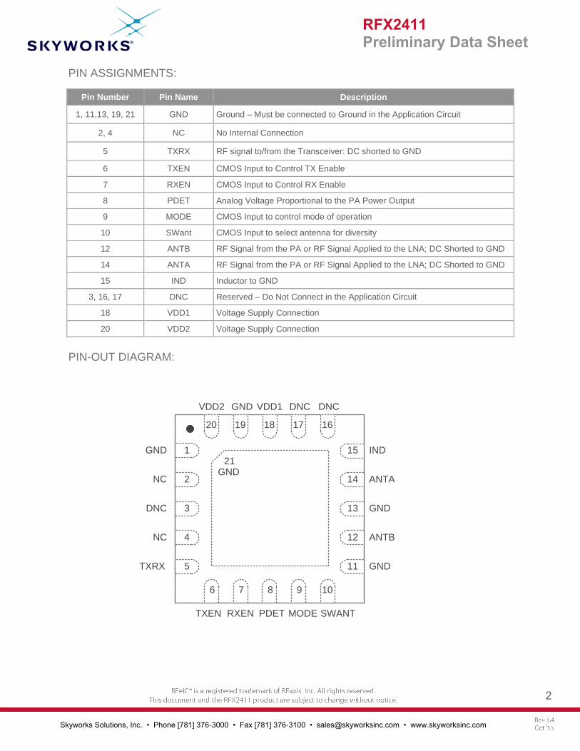
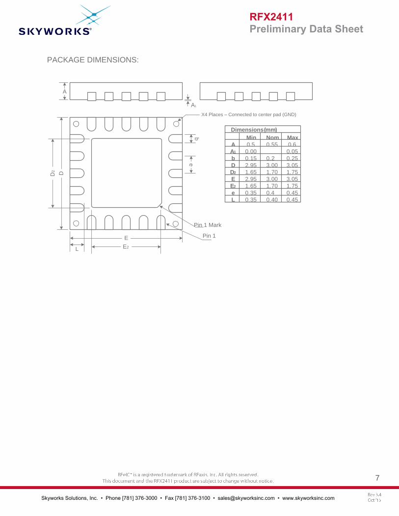
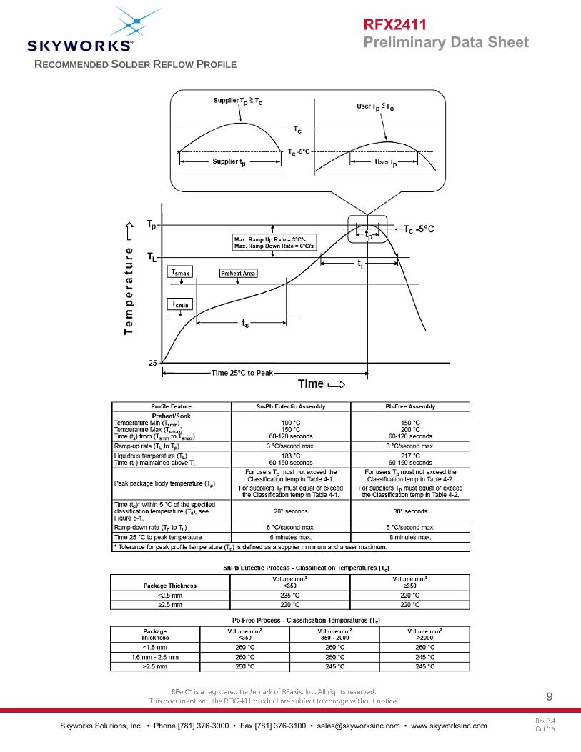
1

Skyworks Solutions, Inc. • Phone [781] 376-3000 • Fax [781] 376-3100 • [email protected] • www.skyworksinc.com

RFX2411 Preliminary Data Sheet

2.4GHZ TRANSMIT / RECEIVE ZIGBEE RFEIC WITH DIVERSITY SWITCH

DESCRIPTION The RFX2411 is a fully integrated, single-chip, single-die RFeIC (RF Front-end Integrated Circuit) which incorporates all the RF functionality needed for wireless ZigBee / smart energy applications. The RFX2411 architecture integrates the PA, LNA, Transmit and Receive switching circuitry, the associated matching network, a harmonic filter and a diversity switch all in a CMOS single-chip device. It also includes a bypass mode to provide maximal level of flexibility for system implementations.

This RFeIC is designed for use in 2.4GHz ISM band and supports the 802.15.4 and ZigBee standard. Typical high power applications include home and industrial automation, smart power, and RF4CE among others. Combining superior performance, high sensitivity and efficiency, low noise, small form factor, and low cost, RFX2411 is the perfect solution for applications requiring extended range and bandwidth. RFX2411 has simple and low-voltage CMOS control logic, and requires minimal external components for system implementation. The PA power detect circuit is also integrated.

FEATURES

2.4GHz ZigBee High Power Single-Chip, Single-

Die RF Front-End IC

Antenna Diversity Switch

2.4GHz Transmit High Power Amplifier with Low-

Pass Harmonic Filter

Low Noise Amplifier

Transmit/Receive Switch Circuitry

High Transmit Signal Linearity Meeting Standards

for OQPSK Modulation

Integrated Power Detector for Transmit Power

Monitor and Control

Low Voltage (1.2V) CMOS Control Logic

ESD Protection Circuitry on All Ports

DC Decoupled RF Ports

Internal RF Decoupling on All VDD Bias Pins

Low Noise Figure for the Receive Channel

Very Low DC Power Consumption

Full On-chip Matching and Decoupling Circuitry

Minimal External Components Required

50-Ohm Input / Output Matching

Market Proven CMOS Technology

3 x 3 x 0.55mm Small Outline QFN-20 Package

with Exposed Ground Pad

APPLICATIONS

ZigBee Extended Range Devices

ZigBee Smart Power

RF4CE Remote Control

Home and Industrial Automation

Custom 2.4GHz Radio Systems

Mobile and Battery ZigBee Systems

NC

GND

1

2

3

4

14

13

12

11

1920 18

GND

21

DNC

GND

GND

DNC

ANTA

VDD2 VDD1

GND

NC ANTB

6 7 8 9

ModePDETRXENTXEN

17 16

5

10

SWant

15

IND

TXRX

DNC

2

Skyworks Solutions, Inc. • Phone [781] 376-3000 • Fax [781] 376-3100 • [email protected] • www.skyworksinc.com

RFX2411 Preliminary Data Sheet

PIN ASSIGNMENTS:

Pin Number Pin Name Description

1, 11,13, 19, 21 GND Ground – Must be connected to Ground in the Application Circuit

2, 4 NC No Internal Connection

5 TXRX RF signal to/from the Transceiver: DC shorted to GND

6 TXEN CMOS Input to Control TX Enable

7 RXEN CMOS Input to Control RX Enable

8 PDET Analog Voltage Proportional to the PA Power Output

9 MODE CMOS Input to control mode of operation

10 SWant CMOS Input to select antenna for diversity

12 ANTB RF Signal from the PA or RF Signal Applied to the LNA; DC Shorted to GND

14 ANTA RF Signal from the PA or RF Signal Applied to the LNA; DC Shorted to GND

15 IND Inductor to GND

3, 16, 17 DNC Reserved – Do Not Connect in the Application Circuit

18 VDD1 Voltage Supply Connection

20 VDD2 Voltage Supply Connection

PIN-OUT DIAGRAM:

DNC

GND

NC

DNC

NC

TXRX

1

2

3

4

5

6 7 8 9 10

11

12

13

14

15

1617181920

21GND

TXEN RXEN PDET MODE SWANT

GND

GND

IND

ANTA

ANTB

VDD1 DNCDNCVDD2 GND

3

Skyworks Solutions, Inc. • Phone [781] 376-3000 • Fax [781] 376-3100 • [email protected] • www.skyworksinc.com

RFX2411 Preliminary Data Sheet

ABSOLUTE MAXIMUM RATINGS:

Parameters Units Min Max Conditions

DC VDD Voltage Supply V 0 4.0 All VDD Pins

DC Control Pin Voltage V 0 3.6 Through 1Kohm resistor

DC VDD Current Consumption mA 350 Through VDD Pins when TX is “ON”

TX RF Input Power dBm +5

ANT RF RX Input Power dBm +5 LNA Mode

ANT RF RX Input Power dBm +16 Bypass Mode

Junction Temperature oC

+150

Storage Ambient Temperature oC -50 +150

No RF and DC Voltages Applied Appropriate care required according to

JEDEC Standards

ESD Voltage (HBM) V > 1000 Human Body Model

Note: Sustained operation at or above the Absolute Maximum Ratings for any one or combinations of

the above parameters may result in permanent damage to the device and is not recommended.

All Maximum RF Input Power Ratings assume 50-Ohm terminal impedance.

RECOMENDED OPERATING CONDITIONS:

Parameters Units Min Typ Max Conditions

DC VDD Voltage Supply (Note 1) V 2.0 3.3 3.6 All VDD Pins

Control Voltage “High” V 1.2 VDD Through 1Kohm resistor

Control Voltage “Low” V 0 0.3

DC Control Pin Current Consumption μA 1 Mode, SWant, TXEN, RXEN

DC Shutdown Current nA 300 Mode, SWant, TXEN, RXEN; Low

PA Turn On/Off Time µsec 1

LNA Turn On/Off Time µsec 1

Antenna Switch Time µsec 1

Operating Ambient Temperature oC -40 +125

See Note 2 ja

oC/W

35

Note 1: VDD1 and VDD2 supply pins are internally connected.

Note2: For operation above +85 oC, use the ja as guidance for system design to assure the junction

temperature will not exceed the maximum of +150 oC.

4

Skyworks Solutions, Inc. • Phone [781] 376-3000 • Fax [781] 376-3100 • [email protected] • www.skyworksinc.com

RFX2411 Preliminary Data Sheet

TRANSMIT TECHNICAL PARAMETERS (VDD=3.3V; T=+25 oC)

Parameters Units Min Typ Max Conditions

Operating Frequency Band GHz 2.4 2.5 All RF Pins Terminated by 50 Ohm

Saturated Output Power dBm +21

Output P1dB dBm +19 CW Input

Small-Signal Gain dB 26 High Idq TX Mode

dB 24 Low Idq TX Mode

Second Harmonic dBc -35 POUT <= +20dBm, CW at ANT Pin

Third Harmonic dBc

-35 POUT <= +20dBm, CW at ANT Pin

Total Supply Current mA 95 POUT = +20dBm, High Idq TX Mode

mA 95 POUT = +20dBm, Low Idq TX Mode

TX Quiescent Current

mA 18 High Idq TX Mode

mA 15 Low Idq TX Mode

Input Return Loss dB -15

Output Return Loss dB -7

Power Detector Voltage V 0.14 Pout = +5dBm, 10kΩ load

V 0.9 Pout = +20dBm, 10kΩ load

Input / Output Impedance Single-Ended Ohm 50

RF Leakage Active Antenna to non-Active Antenna

dB -18 Antenna A/B leaking into Antenna B/A

Load VSWR for Stability (Set Pout=20dBm at 50 ohm)

N/A 6:1 All Non-Harmonically Related Spurs

Less than -60dBm/MHz (CW)

Load VSWR for Ruggedness (Set Pout=20dBm at 50 ohm)

N/A 10:1 No Damage

5

Skyworks Solutions, Inc. • Phone [781] 376-3000 • Fax [781] 376-3100 • [email protected] • www.skyworksinc.com

RFX2411 Preliminary Data Sheet

RECEIVE TECHNICAL PARAMETERS (VDD=3.3V; T=+25 oC)

Parameters Units Min Typ Max Conditions

Operating Frequency Band GHz 2.4 2.5 All RF Pins Terminated by 50 Ohm

Gain dB 14 Low Noise Figure Mode

10 Low Current Mode

Noise Figure dB 2.5 Low Noise Figure Mode

3.5 Low Current Mode

Input P1dB dBm -8 Low Noise Figure Mode

-3 Low Current Mode

RX Quiescent Current mA 9 Low Noise Figure Mode

4 Low Current Mode

RF Port Impedance Ohm 50 At TXRX and ANT Pins

Input Return Loss dB -8 At ANT Pin, Low NF Mode

Output Return Loss dB -12 At TXRX Pin, Low NF Mode

BYPASS MODE TECHNICAL PARAMETERS (VDD=3.3V; T=+25 oC):

Parameters Units Min Typ Max Conditions

Operating Frequency GHz 2.4 2.5

Insertion Loss dB 5

Input P1dB dBm >16 At ANTA or ANTB

Current Consumption nA 700 Through VDD Supply Pins

CONTROL LOGIC TRUTH TABLE

Note: “1” denotes high voltage state (>

1.2V)

“0” denotes low voltage stage (<0.3V) at

Control Pins

“X” denotes do not care: either “1” or “0”

can be applied

PCB LAND PATTERN

TXEN RXEN MODE Mode of Operation

0 0 0 Shutdown Mode

0 0 1 Bypass Mode

1 X 0 Low Idq TX Mode

1 X 1 High Idq TX Mode

0 1 0 Low Noise Figure Receive Mode

0 1 1 Low Current Receive Mode

SWant Mode of Operation

1 ANTA port enabled

0 ANTB port enabled

6

Skyworks Solutions, Inc. • Phone [781] 376-3000 • Fax [781] 376-3100 • [email protected] • www.skyworksinc.com

RFX2411 Preliminary Data Sheet

3.5mm

3.0mm

1.7mm x

1.7mm

0.

0.

0.

0.

0.25mm

0.2 mm 0.4mm

0.65mm

PACKAGE MARKING:

2411

Pin 1 Mark

Second Line

Lot Number

Third Line

Date Code

LLLL.L

AAYYWW

First Line

Part Number

7

Skyworks Solutions, Inc. • Phone [781] 376-3000 • Fax [781] 376-3100 • [email protected] • www.skyworksinc.com

RFX2411 Preliminary Data Sheet

PACKAGE DIMENSIONS:

b

D2

Pin 1 Mark

Pin 1

E2

D

e

E

A1

A

L

A

A1

b

D

D2

E

E2

e

L

Min

0.5

0.00

0.15

2.95

1.65

2.95

1.65

0.35

0.35

Nom

0.55

0.2

3.00

1.70

3.00

1.70

0.4

0.40

Max

0.6

0.05

0.25

3.05

1.75

3.05

1.75

0.45

0.45

Dimensions (mm)

X4 Places – Connected to center pad (GND)

8

Skyworks Solutions, Inc. • Phone [781] 376-3000 • Fax [781] 376-3100 • [email protected] • www.skyworksinc.com

RFX2411 Preliminary Data Sheet

TAPE AND REEL INFORMATION:

9

Skyworks Solutions, Inc. • Phone [781] 376-3000 • Fax [781] 376-3100 • [email protected] • www.skyworksinc.com

RFX2411 Preliminary Data Sheet

RECOMMENDED SOLDER REFLOW PROFILE


Recommended