27
2.5 / 3D Design Solution Scott / Graser 16 / Oct / 2015
| Date post: | 22-Mar-2019 |
| Category: |
Documents |
| Upload: | truongtuong |
| View: | 212 times |
| Download: | 0 times |
2.5 / 3D Design Solution
Scott / Graser 16 / Oct / 2015

Agenda • Introduction - 2.5 / 3D Design Overview • Cadence Virtuoso Custom 3D - IC Design Solution • Summary
Introduction – 2.5 / 3D Design Overview

2.5 / 3D Design Overview
BGA
Package substrate
Interposer C4 bump
U-bump
Silicon/Organic substrate
Board
VRM CAP
PCB
Solder Ball
CAP
Courtesy of TSMC
Logic IC Mem IC
Memory Cube CAP
Logic IC Mem IC
Mem IC
Mem IC

Multiple Pathways to 2.5 / 3D Integration
Packaging Platform Examples Drivers / Applications
Silicon based interposers Die stacking with TSV
Silicon partitioning CPU / GPU – memory I / F High-end computing High-end networking Memory, FPGAs
Fan out wafer level Organic interposers 1
Silicon partitioning Logic / memory integration Mobile convergence AP, BB, modem, PMIC, RF Smart phones & tables
Conventional laminate build-up technologies
Multi-die integration Logic / memory integration Baseband, analog, RF, passive

Advanced Technology Planning & Implementation
Packaging Platform Examples Cadence Solutions
Silicon based interposers Die stacking with TSV
Encounter / Virtuoso /
SIP Layout-XL
Fan out wafer level Organic interposers 1
SIP/APD OrbitIO
APR Conventional laminate build-up technologies

Components of 2.5 / 3D – Silicon Interposer • Silicon interposer: A die made of silicon with vias that connect both sides of
die together for signal / power transmission.
• Micro bumps connects multiple die face-down on silicon interposers. The interposer has multi-layer wiring and TSV.
• It provides a higher level of integration together with system performance improvements.
Package
Chip
Silicon Interposer
Source: http://semiengineering.com
UBM
C4 bumps

Components of 2.5 / 3D – TSV • TSV can be used with 3D Packages (with Si Interposer) or with 3D ICs (where
stacked Si wafer/dies) are connected.
• TSV is etched completely through the silicon substrate, after which it is filled with a conductive material such as copper. After the dielectric and metal patterns have been formed, substrates are thinned to some fraction of their original thickness, then the substrates are bonded together to form one electrical entity.
Source: P. Leduc, LETI, D43D, 2010

Advantages of 2.5 / 3D Shorter Interconnects
• Direct Vertical Communication – Shorter Global / Chip-to-Chip interconnects – Reduced number of global interconnects
• Less Resistance and Capacitance – Less power consumption – Higher performance
Short Time to Market
• Can use optimized standard already available products from different vendors
Heterogeneous Integration
• Exploits the best process technologies for fabrication of different functional blocks
– No yield compromise – Greater functionality
Higher Integration Density
• Integration in horizontal and vertical directions
• Smaller footprint
Source: Roshan Weerasekera, KTH
Cadence Virtuoso Custom 3D-IC Design Solution

Virtuoso Custom 3D-IC Design Flow
IC12.1 “Create Bump and TSV” GUI
Stacked Die file (*.xml)
Bump location
file (*.bump)
Power side file (*.side)
Files dump from EDI
placement of ubump, flip-chip bump & tsv via
alignment of pin labels and bumps
constraint setting and routing
Run PVS for DRC/LVS
Run QRC for extraction
Run post-sim for EM/IR-Drop
analysis
Run Voltus for analyzing
EM/IR-Drop result
Connectivity creation
VerilogIn *.v files
( A.v, B.v, interposer .v top.v)
Create schematic view
interposer layout view creation by
use of (GFS)
Lefin tech(*.tlef) and macro *.lef files
1
Note: 1+2+3: IC12.1 3DIC features
2
3
4

What’s Available in Virtuoso Specifics
• Bump / TSV creation from adjacent die
• Auto-assign the Terminal to Bump
• Utilities to help resolve bump miss-alignment
• Export the Pad Locations / Bump Mapping File for performing the IR drop analysis
• Virtuoso 6.1.6 / ICADV12.1

Wrapper Schematic • Creating Wrapper in Virtuoso Schematic Editor(VSE)
− Top schematic storing connectivity from die to die / interposer.

Creating Bump and TSV from VLS • Create bumps by using a bump location file to transfer bump
information from one die to the adjacent die.
• Create bump arrays on dies such as silicon interposers. You need to assign these bump instances to their respective terminals.

Establishing Connectivity Between Bumps • After creating bumps and TSVs, you establish connectivity between
bumps – Assigning Bump Instances to Terminals – Moving PinFig Objects to Bumps – Creating Bump Labels
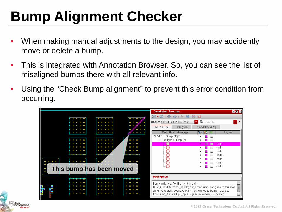
Bump Alignment Checker
This bump has been moved
• When making manual adjustments to the design, you may accidently move or delete a bump.
• This is integrated with Annotation Browser. So, you can see the list of misaligned bumps there with all relevant info.
• Using the “Check Bump alignment” to prevent this error condition from occurring.

Using Co-Design
Synchronize
Editing Die Background: Interposer
Editing Interposer Background: Die
• This allows designer to see one die over another at the same time. For example, you can work on the Interposer actively in one window, with the die visible dimly in the background. And in the second window, it is reverse, i.e. the die is active with Interposer in the background.

Parasitic Extraction Solution • Next-generation Cadence® Quantus™ QRC Extraction Solution
– Up to 5X faster performance for single and multi-corner extraction runs – Scalable to 100s of CPUs / machines – Best-in-its-class down to FinFET accuracy / performance
• New random-walk based field solver, Quantus FS • Fully certified at TSMC for 16nm FinFET

Supports all Design Types with Industry-Leading Functionality
Substrate Noise Analysis (SNA) • Full 3D substrate model • Full chip and block level • Tightly integrated in Virtuoso
Inductance Extraction • Support PEEC method • Sweep from DC100GHz • Supports mutual and Self inductance
MeshR • Used for PowerMos / LCD • Better accuracy for all irregular or wide metal shapes
RLCK Reduction • Supports RC and RCLK redux • 20x simulation time reduction, with 5% accuracy • 2.4x total TAT— good accuracy
Custom / Analog and RF Designs
SerDes
IP / SRAM / Bitcell Characterization
Memory, PowerMos, Image Sensors, etc.

QRC Extracted View—Integration in Virtuoso Platform
Integrated with Virtuoso®
Extracted View • Integrated with Virtuoso® • LVS View Supports PVS, Assura, Calibre • MeshR and substrate extraction for powerMos
Design Debug Environment • Back Annotation • Schematic-Layout Cross-probing
Simulation Analysis • Integrated with Virtuoso ADE • Easy simulation debug • DC simulation for Rdson result
EMIR Analysis • Accurate IR Drop Analysis • Accurate EMIR Analysis & Visualization • Gen models for cell based analysis • Supports Voltus / Voltus-Fi
Faster design closure for custom blocks and top level

Output Format Setup: Extracted View • In extracted view, graphical symbols of parasitic elements
are overlaid onto layout shapes seen by QRC

• The next-generation SoC power signoff platform
Power Calculation
IR-Drop and EM
De-Cap Power Switch
IR-Aware STA (Tempus solution)
Early Rail Analysis (Encounter DIS)
Chip-PKG-PCB (Sigrity™)
Performance
Accuracy
Ca
pa
city
In
teg
ratio
n
Voltus IC Power Integrity Solution

Voltus and Sigrity Chip-PKG-PCB Co-Simulation
• Accurate power signoff for highly coupled power delivery network – Die-model and PKG/PCB-model in broadband SPICE format for “Voltus +
Sigrity” co-simulation – Power map/temperature map for electro-thermal co-analysis – Comprehensive power and signal integrity analysis
Voltus Platform
Sigrity Solution
PKG Model
Die Model
MCP
Temperature Map
Power Map
3D-IC Technology

Chip-Centric Thermal Analysis • Electrical / thermal co-simulation
• Thermal runaway – Positive feedback among chip’s temperature, leakage, and power dissipation – Temperature dependent IR-drop and EM
• Chip-centric thermal co-simulation with “Voltus + Sigrity” – Voltus output: temperature and location dependent “Power Map” file – Sigrity computes detailed temperature distribution for chip-PKG-PCB (T vs. time) – Voltus tool reads back “Temperature Map” file for EMIR convergence – Thermal view available in 2D/3D
Power
Temperature
Leakage Chip-PKG-PCB Temperature
Temperature Map
Power Map
Voltus Sigrity
PKG
PCB
Chip 3 Chip 2
Chip 1

Summary

Summary
Cadence focuses on making you success
Innovative features to address advanced technologies like interposers, FO-WLP, 2.5 / 3D
Delivers comprehensive EMIR solution with Voltus / Sigrity
Up to 5X faster performance for single and multi-corner extraction runs

Thanks


![Visible light 3D printing with epoxidized vegetable oils · 2.5. Photopolymerizableepoxidecompositionphotocatalysedwith curcumin Theformulationofthesolutionwasadaptedfromreference[32].In](https://static.documents.pub/doc/80x56/607cf86bc2defa748c56a83e/visible-light-3d-printing-with-epoxidized-vegetable-oils-25-photopolymerizableepoxidecompositionphotocatalysedwith.jpg)
![jan 2012 · 2017-07-19 · phot 2" x 2.5" photo 2" x 2.5" C) PageMaps photo 2.5" x 2.5" photo 2.5" x 2.5" photo 2.5" x 2.5" photo 2" x 2.5" photo 2.5" x 2.5" C] PageMaps photo 2.5"](https://static.documents.pub/doc/80x56/5f4cb42409b5fa18f7093d11/jan-2012-2017-07-19-phot-2-x-25-photo-2-x-25-c-pagemaps.jpg)


