2674 IEEE JOURNAL OF SOLID-STATE CIRCUITS, VOL. 43, NO. 12, DECEMBER 2008
Transmitter Architectures Based on Near-Field DirectAntenna Modulation
Aydin Babakhani, Member, IEEE, David B. Rutledge, Fellow, IEEE, and Ali Hajimiri, Member, IEEE
Abstract—A near-field direct antenna modulation (NFDAM)technique is introduced, where the radiated far-field signal ismodulated by time-varying changes in the antenna near-fieldelectromagnetic (EM) boundary conditions. This enables thetransmitter to send data in a direction-dependent fashion pro-ducing a secure communication link. Near-field direct antennamodulation (NFDAM) can be performed by using either switchesor varactors. Two fully-integrated proof-of-concept NFDAMtransmitters operating at 60 GHz using switches and varactors aredemonstrated in silicon proving the feasibility of this approach.
I N THE LATE 1800s and early 1900s, wireless transmis-sion of information started its journey. During this period,
inventors such as David E. Hughes, Heinrich Hertz, NikolaTesla, Guglielmo Marconi, Reginald Fessenden, and Edwin H.Armstrong had to work with long wavelengths due to the lackof high frequency amplifiers [1], [2]. At those wavelengths, thesize of an efficient antenna is much larger than the size of the ac-tive devices used. The practical issues involved in implementingsuch large antennas limited the number of effective solutionsfor designing wireless transceivers. Among these solutions,we can mention the invention of the regenerative, heterodyne,and homodyne receivers [1], [2]. With his invention of thesuper-heterodyne receiver in 1918, Armstrong introduced theidea of modulating the signal at low frequencies, or baseband,and up-converting it to the radio frequency (RF). Since then,there have been many breakthroughs in related technologiesincluding the invention of the transistor itself in 1947. However,there have been few fundamental changes in transceiver archi-tectures despite the availability of a broad range of supportingtechnologies; most of today’s high performance systems stilluse ideas based on the heterodyne or homodyne architectures.Today’s silicon technologies provide transistors with unity-cur-rent-gain frequencies in excess of 200 GHz, which makeit possible to implement mm-wave integrated transceivers ona single chip [3]–[10]. At these frequencies, wavelengths arecomparable to the die size and orders of magnitude smaller
Manuscript received April 15, 2008; revised June 25, 2008. Current versionpublished December 10, 2008.
Digital Object Identifier 10.1109/JSSC.2008.2004864
than those used by Armstrong to implement his first hetero-dyne receiver (For instance, a simple half-wavelength dipoleantenna in vacuum is 2.5 mm long at 60 GHz). Access to fastertransistors and the ability to implement antennas on the samedie as analog, RF, and digital circuits encourage reevaluation ofthe classical receiver architectures and exploration of new andfundamentally different architectures. These new architecturesshould deal with system problems across multiple levels ofabstraction, taking full advantage of the greater design space toobtain a more global optimum.
Fig. 1 shows the block diagram of a conventional direct-con-version transmitter. In this architecture, the in-phase (I) andquadrature (Q) signals are modulated at baseband and thenup-converted to radio frequency (RF). The modulated RFsignal goes through a power amplifier (PA) which drives theantenna. It is noteworthy that in this conventional transmitterarchitecture, the already modulated signal couples to the an-tenna. As seen in Fig. 1, in a mostly line-of-sight scheme, areceiver sitting in a side lobe of the antenna receives the sameinformation as the receiver located at the antenna’s main beam.The only differences between the receiver data at different di-rections are the signal power and a time shift. Therefore, givena high-sensitivity receiver it would be possible for a receiver inan unintended direction to eavesdrop on the communication.
We will see in the rest of this paper how near-field direct an-tenna modulation (NFDAM) can be used to overcome the se-curity challenge using a direction-dependent information trans-mission. In Section II we will discuss the concept of NFDAM. InSection III and IV we discuss the switch-based NFDAM, whilein Section V we will investigate the varactor-based version. Wewill review the circuit level details in Section VI and summarizethe measurement results in Section VII.
II. CONCEPT OF NEAR-FIELD DIRECT ANTENNA MODULATION
In the past, directly modulating the antenna has been usedfor different purposes in the literatures. For instance, in [11], amicrostrip patch antenna is fabricated directly on a silicon-sub-strate forming a distributed Schottky diode between the patchand the ground plane. In the same paper, a CW microwave car-rier is modulated by applying a dc bias control between thepatch and the ground. In [12], a patch antenna is integrated withSchottky diodes which are driven by modulating signals. Theswitches are able to shut off and turn on the antenna’s radiatingedges directly to overcome the patch antenna’s bandwidth limi-tation. In this paper, [12], a patch antenna with a resonance fre-quency of 2.4 GHz and a 30 MHz bandwidth is used to transmita digitally modulated signal with 400 MHz bandwidth. It isnoteworthy that although the scheme in [12] shares the same
Authorized licensed use limited to: CALIFORNIA INSTITUTE OF TECHNOLOGY. Downloaded on January 9, 2009 at 13:24 from IEEE Xplore. Restrictions apply.
BABAKHANI et al.: TRANSMITTER ARCHITECTURES BASED ON NEAR-FIELD DIRECT ANTENNA MODULATION 2675
Fig. 1. Conventional transmitter architecture.
Fig. 2. Modulation at baseband.
name (DAM) with our proposed approach, it describes a dif-ferent system that is different from our proposed one that doesnot enhance the communication security. In [13] a discrete elec-tronically steerable parasitic array radiator (ESPAR) antenna isused to increase the fluctuation of the channel characteristics.Only the desired transmitter and receiver share the communica-tion channel characteristics and use the fluctuating channel toprovide a secret key agreement. Unlike our scheme, the key re-mains the same for a large number of bits in this approach.
In our work, a large number of reflectors with many MOSswitches are used to form a near-field direct antenna modula-tion system by creating a large number of degrees of freedom tobe able to generate a broad range of signal constellations witha variety of interesting properties. We will show that, by inte-grating reflectors and switches in the near-field of an on-chipdipole antenna, we are able to transmit information in a direc-tion dependent fashion with a great deal of flexibility and speedfacilitated by the silicon technology.
To illustrate the technique of near-field direct antenna mod-ulation (NFDAM), we need to review the characteristics of theconventional systems which are based on modulation at base-band (Fig. 2). In the absence of multipath, any change at thebaseband appears in the desired direction as well as the un-desired direction (the only difference is the power level and adelay), as illustrated symbolically by the transition from point 1to point 2. This is because the signal is already modulated beforethe antenna and because the antenna pattern does not changequickly.
The proposed NFDAM technique, illustrated in Fig. 3, is fun-damentally different from the one shown in Fig. 2. The NFDAMtransmitter utilizes only a locked RF signal source and a PA todrive the antenna. In this scheme we modulate the phase and
Fig. 3. Modulation after the antenna.
amplitude by changing the antenna characteristics and hence itspattern at the symbol transmission rate. As a result, we are ableto transmit different signals independently to the desired and theundesired directions, unlike the conventional architectures. Inthis case, the information is sent to the desired direction and themisinformation is sent to the undesired direction. It is importantto realize that we need to change the antenna characteristics (itsnear- and far-field) at the symbol rate in order to properly mod-ulate the signal. Next, we introduce two alternative techniquesto vary the antenna boundary conditions thereby changing thephase and amplitude of the antenna far-field pattern.
III. SWITCH-BASED NFDAM
Here we will use a basic and somewhat over-simplified modelto introduce the concept of near-field direct antenna modulationto provide some basic intuition about it. A toy example of thistechnique is shown in Fig. 4. On the left side of Fig. 4, we show adipole antenna with an adjacent reflector in its close proximity.The reflector is composed of two metal pieces connected withan ideal switch. Let us say the main dipole antenna radiates asignal in the z-direction, normal to the plane(bore-sight). Some part of the main signal couples to the adja-cent reflector in the near field of the antenna, causing the re-flector to scatter a signal in the z direction.By closing the switch, we can change the reflector’s effectivelength and scattering properties, which cause the reflected signalto have a different phase and amplitude, . In these two cases thefar-field signal in the z-direction can be calculated by
(1)
(2)
Authorized licensed use limited to: CALIFORNIA INSTITUTE OF TECHNOLOGY. Downloaded on January 9, 2009 at 13:24 from IEEE Xplore. Restrictions apply.
2676 IEEE JOURNAL OF SOLID-STATE CIRCUITS, VOL. 43, NO. 12, DECEMBER 2008
Fig. 4. Signal modulation using switches on the reflectors. (a) Open switch. (b) Closed switch.
Fig. 5. Arbitrary signal modulation.
The real and imaginary parts of the combined signal in thefar-field are shown on the signal constellation diagram (Fig. 4).The example above shows how a simple switch can change thecharacteristics of the reflector and hence perform a crude signalmodulation.
It is important to realize that the aforementioned illustrationis oversimplified. In our system, the reflectors are located inthe near-field of the antenna and hence the propagation-basedrepresentation used here suffers from not capturing the completenear-field electromagnetic behavior of such a system. In realitythese reflectors change the antenna parasitic without necessarily
Fig. 6. Simulation results of the switch-based NFDAM transmitter (10, 000points).
changing the path delay. Changing the antenna parasitic at thenear-field of the antenna modulates the far-field radiated signal.
Consider a practical system in which more than two constel-lation points are required in order to transmit the signal at an ac-ceptable bit-rate. The number of points on the constellation di-agram can be increased by introducing multiple reflectors, eachwith multiple switches, as shown in Fig. 5. For total switches,
constellation points can be generated. Thus, if we have a suf-ficiently large number of switches, it is possible to generate avery large number of constellation points. This is illustrated inFig. 6, where 10,000 random switching combinations are sim-ulated and real and imaginary parts of the induced voltage on areceiving dipole antenna located at the far field are plotted. Fivereflectors are placed at each side of the antenna and nine idealswitches are placed on each reflector, resulting in 90 switches intotal. Based on this simulation, it is possible to cover all of thefour quadrants on the signal constellation diagram.
Authorized licensed use limited to: CALIFORNIA INSTITUTE OF TECHNOLOGY. Downloaded on January 9, 2009 at 13:24 from IEEE Xplore. Restrictions apply.
BABAKHANI et al.: TRANSMITTER ARCHITECTURES BASED ON NEAR-FIELD DIRECT ANTENNA MODULATION 2677
Fig. 7. Communication security. (a) Desired direction. (b) Undesired direction.
Simulation results show that the coverage of the signal con-stellation diagram depends on the performance of the switches.For example, by using switches with off-impedance of 70 in-stead of ideal switches, it is only possible to cover almost onequadrant in the signal constellation diagram. It is also impor-tant to carefully choose the switching combinations to minimizethe impedance variation at the input of the antenna. Based onthe simulation results, if we are willing to tolerate 1.5 dB vari-ation in power gain, 2 dBm variation in delivered power, and3% variation in power added efficiency of the PA, we are stillable to cover one quadrant by using real switches (maximumimpedance of 70 ).
It should be noted that only the carrier signal goes through thePA, so there is no need to design a broadband PA. A locked oscil-lator generates an unmodulated sinusoidal signal that drives thePA. As a result, this system is capable of transmitting broadbandinformation while using a narrowband PA. This system also canutilize highly efficient switching PA in transmission of constantand non-constant envelope-modulated signals. In a silicon im-plementation of the switch-based NFDAM scheme, the switchescan be implemented using small-feature size MOS transistors.
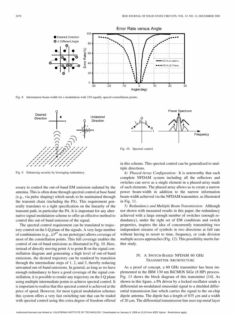
1) Secure Communication Link: As mentioned earlier, oneof the unique characteristics of this system is its ability totransmit independent signals in different directions, as symbol-ically depicted in Fig. 7. To see how this is achieved, assume aset of switching combinations has been found which generatesa 16 QAM at the bore-sight (Fig. 7(a)). If we look at themodulation points in a direction different than the bore-sight(Fig. 7(b)), we will see that the constellation points aretranslated from their original locations to seemingly randomlocations, causing a scrambled set of points on the signalconstellation diagram. This happens because the scatteringproperties of the reflectors and hence the phase and amplitudeof the reflected signal vary with angle. The scrambling propertyprevents undesired receivers from properly demodulating thesignal. At larger angles, some of these constellation pointsmove to adjacent compartments (Fig. 8) and introduce error.Fig. 8 shows the simulated error rate versus angle in the E-plane(parallel to dipole) and the H-plane (normal to dipole) of an
on-chip dipole antenna. In this simulation, 210 equally spacedconstellation points at the bore-sight are selected and viewed atdifferent angles on the E- and H-planes of the antenna. On theH-plane, the error rate rises rapidly and reaches 50% at offsetangles of 2–3 degrees. On the E-plane, the error rate reaches
50% at offset angles of 6–7 degrees off from the bore-sight.Receivers located at angles 1 can completely recover themodulated signal without any error in the absence of noiseand other channel non-idealities. In other words, receiverslocated within the information beam-width of the antenna canproperly recover the signal. Thus, it is necessary to define theinformation beam-width in addition to the power beam-widthfor such systems. The radiation pattern beam-width representsthe power directionality of the beam while the informationbeam-width refers to the information directionality of the beam.
2) Redundancy and Added Security: It was mentionedthat by adding each switch the total number of the switchingcombinations is doubled ( combinations for switches).In our switch-based NFDAM transmitter prototype design, wehave ten reflectors each with nine switches, totalingswitches. This results in combinations. Obviously, itis not necessary to use all of these combinations, but this largenumber of combinations creates so much redundancy that canbe utilized in a productive way.
It is possible to generate a desired phase and amplitude in agiven direction using so many different switch combinations.For a large enough number of combinations, it is possible tofind different switch combinations that produce the same pointin the desired direction while generating widely scattered pointsin other directions (Fig. 9). This property of the system allowsthe transmission of a set of pre-defined modulation points in adesired direction while simultaneously randomly changing thepattern of the constellation points in the undesired directions,thus making it even more challenging for unintended receiversto find a one-to-one mapping between the received signal at thedesired direction and the undesired directions.
3) Spectral Control: In most communication transmitters,not only should one adhere to the specifications on the trans-mitted signal in the frequency band of interest, but it is also nec-
Authorized licensed use limited to: CALIFORNIA INSTITUTE OF TECHNOLOGY. Downloaded on January 9, 2009 at 13:24 from IEEE Xplore. Restrictions apply.
2678 IEEE JOURNAL OF SOLID-STATE CIRCUITS, VOL. 43, NO. 12, DECEMBER 2008
Fig. 8. Information beam-width for a modulation with 210 equally spaced constellation points.
Fig. 9. Enhancing security by leveraging redundancy.
essary to control the out-of-band EM emission radiated by theantenna. This is often done through spectral control at base band(e.g., via pulse shaping) which needs to be maintained throughthe transmit chain (including the PA). This requirement gen-erally translates to a tight specification on the linearity of thetransmit path, in particular the PA. It is important for any alter-native signal modulation scheme to offer an effective method tocontrol this out-of-band emission of the signal.
The spectral control requirement can be translated to trajec-tory control on the I-Q plane of the signals. A very large numberof combinations (e.g., in our prototype) allows coverage ofmost of the constellation points. This full coverage enables thecontrol of out-of-band emissions as illustrated in Fig. 10. Here,instead of directly moving point A to point B on the signal con-stellation diagram and generating a high level of out-of-bandemissions, the desired trajectory can be rendered by transitionthrough the intermediate steps of 1, 2, and 3, thereby reducingunwanted out-of-band emissions. In general, as long as we haveenough redundancy to have a good coverage of the signal con-stellation, it is possible to render any trajectory on the I-Q planeusing multiple intermediate points to achieve spectral control. Itis important to realize that this spectral control is achieved at theprice of speed. However, for most typical modulation schemesthis system offers a very fast switching rate that can be tradedwith spectral control using this extra degree of freedom offered
Fig. 10. Spectral control.
in this scheme. This spectral control can be generalized to mul-tiple directions.
4) Phased-Array Configuration: It is noteworthy that eachcomplete NFDAM system including all the reflectors andswitches can serve as a single element in a phased-array madeof such elements. The phased array allows us to create a narrowpower beam-width in addition to the narrow informationbeam-width achieved via the NFDAM transmitter, as illustratedin Fig. 11.
5) Redundancy and Multiple Beam Transmission: Althoughnot shown with measured results in this paper, the redundancyachieved with a large enough number of switches (enough re-dundancy), under the right set of EM conditions and switchproperties, inspires the idea of concurrently transmitting twoindependent streams of symbols in two directions at full ratewithout having to resort to time, frequency, or code divisionmultiple access approaches (Fig. 12). This possibility merits fur-ther study.
IV. A SWITCH-BASED NFDAM 60 GHZ
TRANSMITTER ARCHITECTURE
As a proof of concept, a 60 GHz transmitter has been im-plemented in the IBM 130 nm BiCMOS SiGe (8 HP) process.Fig. 13 shows the block diagram of this transmitter [14]. Asshown in this figure, a PA driven by a locked oscillator sends adifferential un-modulated sinusoidal signal to a shielded differ-ential transmission line which carries the signal to the on-chipdipole antenna. The dipole has a length of 835 m and a widthof 20 m. The differential transmission line uses top metal layer
Authorized licensed use limited to: CALIFORNIA INSTITUTE OF TECHNOLOGY. Downloaded on January 9, 2009 at 13:24 from IEEE Xplore. Restrictions apply.
BABAKHANI et al.: TRANSMITTER ARCHITECTURES BASED ON NEAR-FIELD DIRECT ANTENNA MODULATION 2679
Fig. 11. NFDAM transmitter in a phased-array configuration.
for the signal line, for the bottom ground line, andfor the side ground shield. The on-chip dipole antennas and re-flectors are all implemented on lower metal layers , ,and . Five reflectors are placed at each side of the antennaand 9 switches are placed on each reflector resulting in a totalnumber of 90 switches. The antenna and reflectors occupy anarea of 1.3 1.5 mm . As shown in Fig. 13, the baseband datagoes through a digital control unit which controls the state ofswitches.
In the switch-based NFDAM architecture, one of the impor-tant parameters that needs to be optimized is the distance of thereflectors from the antenna. If the reflectors are placed too farfrom the main antenna, the reflected signal will be very weak
not being able to change the phase and amplitude of the mainsignal significantly. On the other hand, if we place reflectors tooclose to the antenna, the size of the aperture will be very smalland the system will not be able to excite a sufficient numberof radiation modes to transmit independent information to sev-eral directions simultaneously. In this design, the locations ofthe reflectors and their distance to the main antenna have beenoptimized. We have implemented a general purpose system ca-pable of generating any arbitrary digitally modulated signal. Fora specific modulation, for example 16 QAM, we may not needto use all of the switches.
As a part of the system, an optional coarse control unit wasimplemented as shown in Fig. 14. This optional unit can be
Authorized licensed use limited to: CALIFORNIA INSTITUTE OF TECHNOLOGY. Downloaded on January 9, 2009 at 13:24 from IEEE Xplore. Restrictions apply.
2680 IEEE JOURNAL OF SOLID-STATE CIRCUITS, VOL. 43, NO. 12, DECEMBER 2008
Fig. 12. The idea of multiple beam transmission by using a single transmitter (not simulation results).
Fig. 13. Details of the switch-based NFDAM transmitter architecture.
used as a quadrant selector with control signals and takingvalues 1 and . In this mode of operation, switches on the re-flectors can be used to generate the constellation points insideeach quadrant and the optional coarse control unit can be usedto choose the quadrant on the signal constellation diagram.
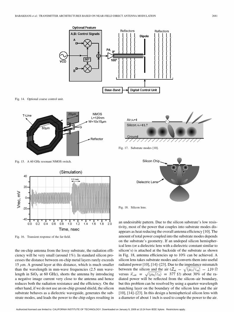
Fig. 15 shows the design of the switch itself. In order toachieve a low on impedance (1–5 ) between the drain and thesource of the switch in its closed state , the switchsize cannot be small. This results in large gate-drain, , andgate-source, , capacitances. The NMOS switch used in thisdesign has an effective width of 150 m as shown in Fig. 15. Toresonate out the switch capacitance and achieve high impedance
in the open state , a circular shielded transmissionline behaving as an inductor is placed between the drain andthe source of the switch. This transmission line resonates withthe open-switch capacitance at 60 GHz resulting in a maximumimpedance of 70 . The circular transmission line has a diam-eter of 60 m and is implemented on metal layers , , and
.One of the main issues which has to be addressed is the tran-
sient response of the switches and the reflectors. This deter-mines the speed at which far-field varies and hence determinesthe maximum symbol modulation rate. The limitation comesfrom two independent factors. The first one is related to the fi-nite time which the wave needs to travel between the antennaand the reflectors and the second is related to the transient re-sponse of the switch. Fig. 16 shows the simulation results of thefar-field’s transient response to a change in the switching com-bination when ideal switches are used. As shown in this figure,the far-field takes less than 200 ps to adapt to a new switchingcombination. This simulation shows that the effective transientresponse of the whole system is limited by the transient time ofthe switch itself, as the switch response is usually longer than200 ps. By designing a switch with a transient response of about800 ps we can achieve a symbol rate of better than 1 GS/s.
One of the important disadvantages of silicon-based on-chipantennas is the low antenna efficiency. This is a result of twofactors; silicon’s high dielectric constant , and sub-strate’s low resistivity (1–10 ). The high level of dopingrequired to fabricate active circuits limits the silicon substrate’sresistivity. Silicon’s high dielectric constant and its large sub-strate thickness (200–300 m) couple most of the dipole outputpower into substrate-modes in unshielded structures as shownin Fig. 17 [10]. If we use an on-chip ground shield to isolate
Authorized licensed use limited to: CALIFORNIA INSTITUTE OF TECHNOLOGY. Downloaded on January 9, 2009 at 13:24 from IEEE Xplore. Restrictions apply.
BABAKHANI et al.: TRANSMITTER ARCHITECTURES BASED ON NEAR-FIELD DIRECT ANTENNA MODULATION 2681
Fig. 14. Optional coarse control unit.
Fig. 15. A 60 GHz resonant NMOS switch.
Fig. 16. Transient response of the far-field.
the on-chip antenna from the lossy substrate, the radiation effi-ciency will be very small (around 1%). In standard silicon pro-cesses the distance between on-chip metal layers rarely exceeds15 m. A ground layer at this distance, which is much smallerthan the wavelength in mm-wave frequencies (2.5 mm wave-length in SiO at 60 GHz), shorts the antenna by introducinga negative image current very close to the antenna and hencereduces both the radiation resistance and the efficiency. On theother hand, if we do not use an on-chip ground shield, the siliconsubstrate behaves as a dielectric waveguide, generates the sub-strate modes, and leads the power to the chip edges resulting in
Fig. 17. Substrate modes [10].
Fig. 18. Silicon lens.
an undesirable pattern. Due to the silicon substrate’s low resis-tivity, most of the power that couples into substrate modes dis-appears as heat reducing the overall antenna efficiency [10]. Theamount of total power coupled into the substrate modes dependson the substrate’s geometry. If an undoped silicon hemispher-ical lens (or a dielectric lens with a dielectric constant similar tosilicon’s) is attached at the backside of the substrate as shownin Fig. 18, antenna efficiencies up to 10% can be achieved. Asilicon lens takes substrate modes and converts them into usefulradiated power [10], [14]–[23]. Due to the impedance mismatchbetween the silicon and the air (versus ) about 30% of the ra-diated power will be reflected from the silicon–air boundary,but this problem can be resolved by using a quarter-wavelengthmatching layer on the boundary of the silicon lens and the air[10], [14]–[23]. In this design a hemispherical silicon lens witha diameter of about 1 inch is used to couple the power to the air.
Authorized licensed use limited to: CALIFORNIA INSTITUTE OF TECHNOLOGY. Downloaded on January 9, 2009 at 13:24 from IEEE Xplore. Restrictions apply.
2682 IEEE JOURNAL OF SOLID-STATE CIRCUITS, VOL. 43, NO. 12, DECEMBER 2008
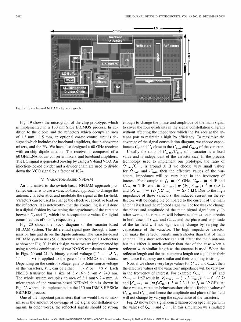
Fig. 19. Switch-based NFDAM chip micrograph.
Fig. 19 shows the micrograph of the chip prototype, whichis implemented in a 130 nm SiGe BiCMOS process. In ad-dition to the dipole and the reflectors which occupy an areaof 1.3 mm 1.5 mm, an optional coarse control unit is de-signed which includes the baseband amplifiers, the up-convertermixers, and the PA. We have also designed a 60 GHz receiverwith on-chip dipole antenna. The receiver is composed of a60 GHz LNA, down-converter mixers, and baseband amplifiers.The LO signal is generated on-chip by using a V-band VCO. Aninjection-locked divider and a divider chain are used to dividedown the VCO signal by a factor of 1024.
V. VARACTOR-BASED NFDAM
An alternative to the switch-based NFDAM approach pre-sented earlier is to use a varactor-based approach to change theantenna characteristics and modulate the signal at the far-field.Varactors can be used to change the effective capacitive load onthe reflectors. It is noteworthy that the controlling is still donein a digital fashion by switching the capacitance of the varactorbetween and , which are the capacitance values for digitalcontrol values of 0 or 1, respectively.
Fig. 20 shows the block diagram of the varactor-basedNFDAM system. The differential signal goes through a trans-mission line and drives the dipole antenna. The varactor-basedNFDAM system uses 90 differential varactors on 10 reflectorsas shown in Fig. 20. In this design, varactors are implemented byusing a series combination of two NMOS transistors as shownin Figs. 20 and 21. A binary control voltage ( '` ,
'` ) is applied to the gate of the NMOS transistors.Depending on the control voltage, gate to drain-source voltageof the varactors, , can be either or . EachNMOS transistor has a size of 3 16 5 m 240 nm.The whole system occupies an area of 2.1 mm 2.4 mm. Amicrograph of the varactor-based NFDAM chip is shown inFig. 22 where it is implemented in the 130 nm IBM 8 HP SiGeBiCMOS process.
One of the important parameters that we would like to max-imize is the amount of coverage of the signal constellation di-agram. In other words, the reflected signals should be strong
enough to change the phase and amplitude of the main signalto cover the four quadrants in the signal constellation diagramwithout affecting the impedance which the PA sees at the an-tenna port to maintain a high PA efficiency. To maximize thecoverage of the signal constellation diagram, we choose capac-itances and close to the and of the varactor.
Usually the ratio of of a varactor is a fixedvalue and is independent of the varactor size. In the processtechnology used to implement our prototype, the ratio of
is around 3. If we choose very small valuesfor and then the effective values of the var-actors’ impedance will be very high in the frequency ofinterest. For example at GHz, fF and
fF result inand . Due to the highimpedance of these varactors, the induced current on the re-flectors will be negligible compared to the current of the mainantenna itself and the reflected signal will be too weak to changethe phase and amplitude of the main signal significantly. Inother words, the varactors will behave as almost open circuitsin both cases of and and the phase and amplitudeof the far-field will not significantly change by varying thecapacitance of the varactor. The high impedance varactorcan make the reflector length much shorter than that of mainantenna. This short reflector can still affect the main antennabut this effect is much smaller than that of the case when areflector with similar length as the antenna is used. When thereflector length and the main antenna length are equal then theirresonance frequency are similar and their coupling is strong.
Now, if we choose very large values for and , thenthe effective values of the varactors’ impedance will be very lowin the frequency of interest. For example pF and
pF result inand at GHz. Atthese values, varactors behave as short circuits for both values of
and and hence the amplitude and phase of far-fieldwill not change by varying the capacitance of the varactors.
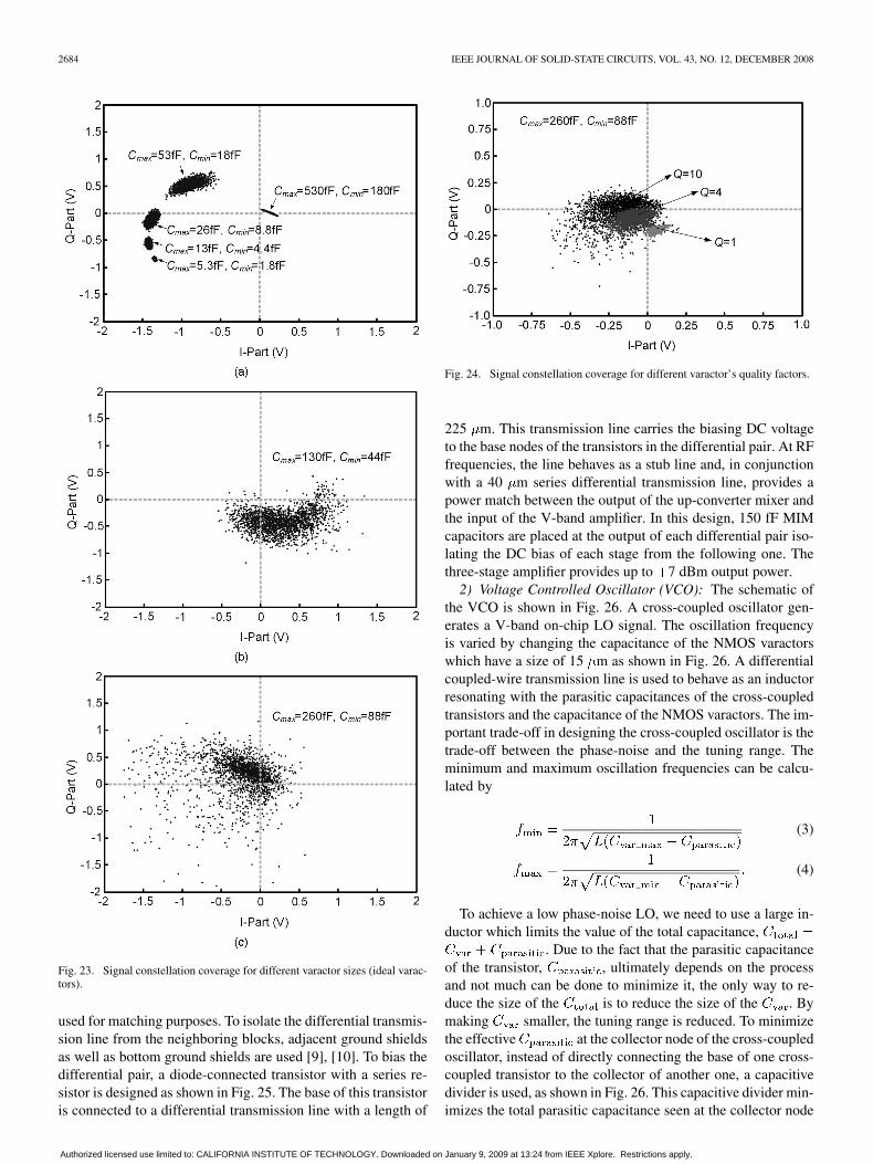
Fig. 23 shows how signal constellation coverage changes withthe values of and . In this simulation we simulated
Authorized licensed use limited to: CALIFORNIA INSTITUTE OF TECHNOLOGY. Downloaded on January 9, 2009 at 13:24 from IEEE Xplore. Restrictions apply.
BABAKHANI et al.: TRANSMITTER ARCHITECTURES BASED ON NEAR-FIELD DIRECT ANTENNA MODULATION 2683
2000 random points, and for each point, for each switchingcombination, we plotted the real and imaginary parts of thevoltage of a dipole antenna located at the far-field. At each pointa Matlab program assigns a random binary value for the ca-pacitance of each varactor, , andplots the real and imaginary parts of the dipole’s voltage locatedat the bore-sight. As shown in Fig. 23(a), for very small var-actor sizes and very large ones the spread of the points on thesignal constellation diagram is very limited. As mentioned be-fore, this is because of the fact that very small varactors behaveas open circuits and very large ones behave as short circuits at60 GHz. Fig. 23(b) and (c) show the spread of the constellationpoints for varactor sizes ( fF, fF) and( fF, fF). As shown in Fig. 23(c), withvaractor size of ( fF, fF) it is easily
Fig. 22. Varactor-based NFDAM’s chip micrograph.
possible to cover all of the four quadrants with binary control-ling of the varactors ( '` , '` ). It is importantto mention that in the above simulations ideal varactors (infiniteQ) are used. Simulations results show that varactors with smallerquality factor reduce the coverage of the signal constellation di-agram. Fig. 24 shows the simulation results for varactors’ sizeof ( fF, fF) with quality factors of 1, 4,and 10. Based on these results, the coverage of the signal con-stellation diagram is a strong function of the varactors’ qualityfactor, . In this simulation a silicon lens is used to minimizethe substrate modes and efficiently couple the signal to the air.
VI. SCHEMATIC OF THE BLOCKS USED IN THE SWITCH-BASED
NFDAM TRANSMITTER
1) V-Band Amplifier: Fig. 25 shows the schematic of theV-band amplifier which is composed of three differential stages.Stub-tuning and coupled-wire differential transmission lines are
Authorized licensed use limited to: CALIFORNIA INSTITUTE OF TECHNOLOGY. Downloaded on January 9, 2009 at 13:24 from IEEE Xplore. Restrictions apply.
2684 IEEE JOURNAL OF SOLID-STATE CIRCUITS, VOL. 43, NO. 12, DECEMBER 2008
Fig. 23. Signal constellation coverage for different varactor sizes (ideal varac-tors).
used for matching purposes. To isolate the differential transmis-sion line from the neighboring blocks, adjacent ground shieldsas well as bottom ground shields are used [9], [10]. To bias thedifferential pair, a diode-connected transistor with a series re-sistor is designed as shown in Fig. 25. The base of this transistoris connected to a differential transmission line with a length of
Fig. 24. Signal constellation coverage for different varactor’s quality factors.
225 m. This transmission line carries the biasing DC voltageto the base nodes of the transistors in the differential pair. At RFfrequencies, the line behaves as a stub line and, in conjunctionwith a 40 m series differential transmission line, provides apower match between the output of the up-converter mixer andthe input of the V-band amplifier. In this design, 150 fF MIMcapacitors are placed at the output of each differential pair iso-lating the DC bias of each stage from the following one. Thethree-stage amplifier provides up to 7 dBm output power.
2) Voltage Controlled Oscillator (VCO): The schematic ofthe VCO is shown in Fig. 26. A cross-coupled oscillator gen-erates a V-band on-chip LO signal. The oscillation frequencyis varied by changing the capacitance of the NMOS varactorswhich have a size of 15 m as shown in Fig. 26. A differentialcoupled-wire transmission line is used to behave as an inductorresonating with the parasitic capacitances of the cross-coupledtransistors and the capacitance of the NMOS varactors. The im-portant trade-off in designing the cross-coupled oscillator is thetrade-off between the phase-noise and the tuning range. Theminimum and maximum oscillation frequencies can be calcu-lated by
(3)
(4)
To achieve a low phase-noise LO, we need to use a large in-ductor which limits the value of the total capacitance,
. Due to the fact that the parasitic capacitanceof the transistor, , ultimately depends on the processand not much can be done to minimize it, the only way to re-duce the size of the is to reduce the size of the . Bymaking smaller, the tuning range is reduced. To minimizethe effective at the collector node of the cross-coupledoscillator, instead of directly connecting the base of one cross-coupled transistor to the collector of another one, a capacitivedivider is used, as shown in Fig. 26. This capacitive divider min-imizes the total parasitic capacitance seen at the collector node
Authorized licensed use limited to: CALIFORNIA INSTITUTE OF TECHNOLOGY. Downloaded on January 9, 2009 at 13:24 from IEEE Xplore. Restrictions apply.
BABAKHANI et al.: TRANSMITTER ARCHITECTURES BASED ON NEAR-FIELD DIRECT ANTENNA MODULATION 2685
Fig. 25. Schematic of the V-band power amplifier.
Fig. 26. Schematic of the V-band VCO.
by minimizing the contribution of the parasitic capacitors con-nected to the base of the cross-coupled transistors. The capaci-tive divider also allows a higher voltage swing at the collectornode of the transistor by isolating that node from the base nodeof the transistor. The high voltage swing improves the phasenoise of the oscillator. To further reduce the parasitic capaci-tance at the collector node, the output signal is taken from thebase node by connecting the load to the base node instead of thecollector node. 91 fF AC-coupling MIM capacitors are used toconnect the output of the oscillator to a following amplifier. Tobias the VCO, a current source and a diode-connected transistorare used as shown in Fig. 26.
3) Injection-Locked Divider: To divide down the LO signaland lock it to a reference signal, we have used an injection-locked divider in combination with a digital divider chain. The
Fig. 27. Schematic of the V-band injection locked divider.
divider chain with the injection locked divider provides a di-viding ratio of 1024 allowing an off-chip low-frequency signalto be locked with the on-chip LO signal.
The VCO, injection locked divider, and divider chain are allimplemented on chip. This allows for an off-chip charge-pump/low-pass filter to be used to lock the oscillator to a lower fre-quency reference externally using a phased-locked loop.
The design of the injection-locked oscillator is similar to thatof the VCO but its load is tuned to provide a self-oscillationfrequency of around . The LO signal is injected at thecurrent source of the cross-coupled pair, as shown in Fig. 27.A single-ended transmission line with length of 220 m andan ac-coupling capacitor with size of 148 fF are used to main-tain a power match between the divider and the preceding stage.The preceding stage is an LO distributor amplifier which isdiscussed next.
Authorized licensed use limited to: CALIFORNIA INSTITUTE OF TECHNOLOGY. Downloaded on January 9, 2009 at 13:24 from IEEE Xplore. Restrictions apply.
2686 IEEE JOURNAL OF SOLID-STATE CIRCUITS, VOL. 43, NO. 12, DECEMBER 2008
Fig. 28. Schematic of the LO distributor amplifier.
Fig. 29. Up-converter mixer and buffer (optional feature).
4) LO Distributor Amplifier: Several LO distributor ampli-fiers are used to provide LO signal to the injection-locked di-vider and up-convertor mixers in the transmitter. The schematicof the LO distributor amplifier is shown in Fig. 28. The LOsignal enters through a stub-matching network and is amplifiedby a cascode differential pair. To distribute the LO signal, thecollector current of the input differential pair is divided equallybetween two identical cascode pairs. These pairs amplify the LOsignal and use stub-tuning to efficiently deliver the LO power tothe following stages.
Up-Convertor Mixer: As an optional feature in our system,up-convertor mixers are designed and used in the optionalcoarse control unit. The coarse control unit can be used as aquadrant-selector on the signal constellation diagram. Fig. 29shows the schematic of the up-convertor mixer. Differentialbaseband or control signals are connected to the base nodes ofthe differential pair as shown in Fig. 29. Stub-tuning is usedat the RF and LO nodes to maintain a power match betweenthe mixer and the adjacent blocks. To amplify the signal at theoutput of the mixer, a differential cascode buffer amplifier is
Authorized licensed use limited to: CALIFORNIA INSTITUTE OF TECHNOLOGY. Downloaded on January 9, 2009 at 13:24 from IEEE Xplore. Restrictions apply.
BABAKHANI et al.: TRANSMITTER ARCHITECTURES BASED ON NEAR-FIELD DIRECT ANTENNA MODULATION 2687
Fig. 30. Measurement setup.
designed as shown in Fig. 29. A 320 m differential transmis-sion line and 148 fF MIM ac-coupling capacitors are used tomatch the output of the mixer to the input of the buffer.
VII. MEASUREMENT RESULTS
A block diagram of the measurement setup is shown inFig. 30. In the first measurement, the on-chip transmitter isdisconnected (with laser trimming) from the antenna-reflec-tors combination and the electromagnetic structure itself istested using an Agilent N5250A network analyzer. A LabViewprogram [24] controls the state of the switches (switch-basedNFDAM) and varactors (varactor-based NFDAM) through adata acquisition card. The data acquisition card sends the digitalstream to the on-chip digital control unit and this unit programsthe switches and the varactors. After sending the desired datastreams and programming the chip, the LabView programcommunicates with the network analyzer through a GPIB card.One of the ports of the network analyzer sends the V-bandsignal through a 1.85 mm cable and connectors to the on-chipantenna and the other port uses a standard horn antenna at thereceiving side to accurately measure the phase and amplitudeof the .
By changing the switching combinations in the switch-basedNFDAM chip, we can accurately measure the variation in thephase and amplitude of the and plot the real and imaginaryparts of the on the signal constellation diagram as shown inFig. 31. In this figure, we have measured the variations of intwo different directions with an angular separation of approxi-mately 90 for the same set of switching combinations. We havemeasured about 2000 randomly chosen switching combinationsand selected the ones which result in 20 equally spaced con-stellation points in the desired direction. As shown in Fig. 31,the signal constellation points are completely scrambled in theundesired direction, proving the functionality of our system.To have a better look at the constellation points, we have usedvertical color-coding to separate these 20 points into several
Fig. 31. Measured constellation points of the switch-based NFDAM chip. Inthis measurement only the switches are used.
groups. This color-coding, and also the numbering of the con-stellation points, help us to better understand the scrambling na-ture of the system.
A picture of the measurement setup is shown in Fig. 32. Theoptional quadrant-selector unit in conjunction with the reflectorswitching is used to cover the four quadrants on the signal con-stellation diagram. Fig. 33 shows the measurement results of thefull coverage of the four quadrants. We have verified the repeata-bility of -parameter measurement in several different ways. Inone case, we have kept sending a fixed set of switching combi-nations for one thousand times. This measurement, which wasperformed over the course of 10 hours, gave us an estimation oferror in the -parameter measurement. This error which is muchsmaller than the distance of two adjacent points in Fig. 33, in-cludes the effects of temperature change, supply voltage noise,and other inaccuracies.
To measure the output power of the transmitter and charac-terize its linearity, the antenna is disconnected from the PA. A1.85 mm coaxial wafer probe, an Agilent V-band power sensor(V8684A), and an Agilent V-band power (E4418B) meter are
Authorized licensed use limited to: CALIFORNIA INSTITUTE OF TECHNOLOGY. Downloaded on January 9, 2009 at 13:24 from IEEE Xplore. Restrictions apply.
2688 IEEE JOURNAL OF SOLID-STATE CIRCUITS, VOL. 43, NO. 12, DECEMBER 2008
Fig. 32. Picture of the measurement setup.
Fig. 33. Measurement results of the four-quadrant coverage of the signal con-stellation space using the optional quadrant-selector and switches (switch-basedNFDAM chip).
used to measure the output power of the transmitter. The inputsignal is generated by an Agilent signal source (E8257D) andapplied to the input of the transmitter through a wafer probe.Fig. 34 shows the measured output power and gain versus theinput power of the transmitter. A transmitter output power of
7 dBm, a small-signal gain of 33dB, and a saturated gain of25 dB are achieved.
In order to measure the VCO performance, a GSG test padconnecting to an on-chip LO signal is designed and used. AnAgilent spectrum analyzer (E4448A) and a SpacekLabs off-chipdown-convertor (GE-590) are used to measure the phase-noiseand tuning range of the VCO. A phase-noise of 100 dBc at10 MHz offset and a tuning range of more than 2.5 GHz areachieved in the measurement.
To measure the performance of the varactor-based NFDAMchip, a setup similar to Fig. 30 is used. Fig. 35 shows the mea-sured constellation points at the received antenna. In this mea-surement, the LabView program changes the pattern of the var-actors by generating about 1400 random combinations and plots
Fig. 34. Conversion gain and pout versus input power.
Fig. 35. Measured constellation points in varactor-based NFDAM chip.
the real and imaginary parts of measured by the AgilentN5250A network analyzer. This measurement proves the func-tionality of the varactor-based NFDAM system.
Compared to resonant switches, varactors do not require thecircular transmission line to resonate their parasitic elements
Authorized licensed use limited to: CALIFORNIA INSTITUTE OF TECHNOLOGY. Downloaded on January 9, 2009 at 13:24 from IEEE Xplore. Restrictions apply.
BABAKHANI et al.: TRANSMITTER ARCHITECTURES BASED ON NEAR-FIELD DIRECT ANTENNA MODULATION 2689
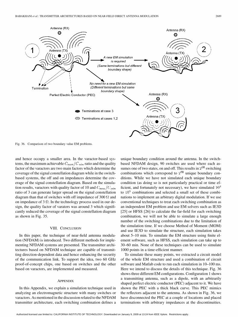
Fig. 36. Comparison of two boundary value EM problems.
and hence occupy a smaller area. In the varactor-based sys-tems, the maximum achievable ratio and the qualityfactor of the varactors are two main factors which determine thecoverage of the signal constellation diagram while in the switch-based systems, the off and on impedances determine the cov-erage of the signal constellation diagram. Based on the simula-tion results, varactors with quality factor of 10 andratio of 3 can generate larger spread on the signal constellationdiagram than that of switches with off impedance of 300 andon impedance of 3 . In the technology process used in our de-sign, the quality factor of varators was around 3 which signifi-cantly reduced the coverage of the signal constellation diagramas shown in Fig. 35.
VIII. CONCLUSION
In this paper, the technique of near-field antenna modula-tion (NFDAM) is introduced. Two different methods for imple-menting NFDAM systems are presented. The transmitter archi-tectures based on NFDAM technique are capable of transmit-ting direction-dependent data and hence enhancing the securityof the communication link. To support the idea, two 60 GHzproof-of-concept chips, one based on switches and the otherbased on varactors, are implemented and measured.
APPENDIX
In this Appendix, we explain a simulation technique used inanalyzing an electromagnetic structure with many switches orvaractors. As mentioned in the discussion related to the NFDAMtransmitter architecture, each switching combination defines a
unique boundary condition around the antenna. In the switch-based NFDAM design, 90 switches are used where each as-sumes one of two states, on and off. This results in switchingcombinations which correspond to unique boundary con-ditions. While we have not simulated each unique boundarycondition (as doing so is not particularly practical or time ef-ficient, and fortunately not necessary), we have simulatedto combinations and selected a small set of these combi-nations to implement an arbitrary digital modulation. If we useconventional techniques to treat each switching combination asan independent EM problem and use EM solvers such as IE3D[25] or HFSS [26] to calculate the far-field for each switchingcombination, we will not be able to simulate a large enoughnumber of the switching combinations due to the limitation ofthe simulation time. If we choose Method of Moment (MOM)and use IE3D to simulate the structure, each simulation takesabout 5–10 min. To simulate the EM structure using finite el-ement software, such as HFSS, each simulation can take up to30–60 min. None of these techniques can be used to simulate1000 points in a time-efficient manner.
To simulate these many points, we extracted a circuit modelof the whole EM structure and used a combination of circuitsoftware and Matlab code to run each simulation in 10–100 ms.Here we intend to discuss the details of this technique. Fig. 36shows three different EM configurations. Configuration 1 showsa transmitting antenna, such as a dipole, with an arbitrarilyshaped perfect electric conductor (PEC) adjacent to it. We haveshown the PEC with a thick black curve. This PEC mimicsthe reflectors adjacent to the antenna. As shown in Fig. 36, wehave disconnected the PEC at a couple of locations and placedterminations with arbitrary impedances at the discontinuities.
Authorized licensed use limited to: CALIFORNIA INSTITUTE OF TECHNOLOGY. Downloaded on January 9, 2009 at 13:24 from IEEE Xplore. Restrictions apply.
2690 IEEE JOURNAL OF SOLID-STATE CIRCUITS, VOL. 43, NO. 12, DECEMBER 2008
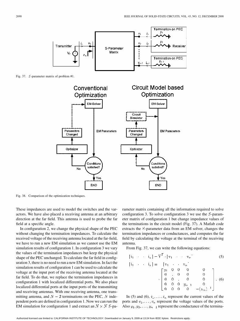
Fig. 37. �-parameter matrix of problem #1.
Fig. 38. Comparison of the optimization techniques.
These impedances are used to model the switches and the var-actors. We have also placed a receiving antenna at an arbitrarydirection at the far field. This antenna is used to probe the farfield at a specific angle.
In configuration 2, we change the physical shape of the PECwithout changing the termination impedances. To calculate thereceived voltage of the receiving antenna located at the far-field,we have to run a new EM simulation as we cannot use the EMsimulation results of configuration 1. In configuration 3 we varythe values of the termination impedances but keep the physicalshape of the PEC unchanged. To calculate the far field in config-uration 3, there is no need to run a new EM simulation. In fact thesimulation results of configuration 1 can be used to calculate thevoltage at the input port of the receiving antenna located at thefar field. To do that, we replace the termination impedances inconfiguration 1 with localized differential ports. We also placelocalized differential ports at the input ports of the transmittingand receiving antennas. With one receiving antenna, one trans-mitting antenna, and terminations on the PEC, inde-pendent ports are defined in configuration 1. Now we can run theEM simulation for configuration 1 and extract an -pa-
rameter matrix containing all the information required to solveconfiguration 3. To solve configuration 3 we use the -param-eter matrix of configuration 1 but change impedance values ofthe terminations in the circuit model (Fig. 37). A Matlab codeextracts the -parameter data from an EM solver, changes thetermination impedances or conductances, and computes the farfield by calculating the voltage at the terminal of the receivingantenna.
From Fig. 37, we can write the following equations:
(5)
(6)
In (5) and (6), represent the current values of theports and represent the voltage values of the ports.Also represent the conductance of the termina-
Authorized licensed use limited to: CALIFORNIA INSTITUTE OF TECHNOLOGY. Downloaded on January 9, 2009 at 13:24 from IEEE Xplore. Restrictions apply.
BABAKHANI et al.: TRANSMITTER ARCHITECTURES BASED ON NEAR-FIELD DIRECT ANTENNA MODULATION 2691
Fig. 39. Patch optimization problem.
Fig. 40. Optimized S11 versus frequency (patch problem).
tions, represents the termination conductance of the receivingantenna, and represents the impedance seen at the input portof the transmitting antenna. is the transposed -parametermatrix of the system and can be calculated from the -param-eter data by the following equation:
(7)
In (7), is the nominal impedance (50 ), is the identitymatrix, is the -parameter matrix, and is the inverse ofthe -parameter matrix.
In (5), (6), and (7), we have unknowns and equationsand hence have a unique nonzero solution. The unknown pa-rameters are , and the known onesare . is the input voltage of the transmittingantenna which is a known parameter. Fig. 38 shows the com-parison between the conventional and the circuit-model basedoptimization techniques in a block flowchart form. In the con-ventional scheme, one EM simulation is required for each iter-ation. However, in the circuit-model-based technique, we onlyneed to run a single EM simulation for the whole optimization
problem. Due to the fact that most of the simulation time is con-sumed by the EM solver, the circuit-model based scheme runsorders of magnitude faster than that of the conventional method.
To highlight the advantage of the above technique we haveoptimized a simple patch antenna by using these two tech-niques. Fig. 39 shows a simple patch optimization problem.The edge-fed patch with a ground shield is composed of 9square metal pieces. We have connected these metal squaresby using 12 terminations, as shown in Fig. 39. The opti-mization goal is to maximize the patch bandwidth by findingoptimum impedance values for the terminations. The rangeof the impedances is chosen based on the practical values ofthe surface mount inductors and capacitors. Our circuit-modelbased Matlab code uses golden section search and parabolicinterpolation to find an optimal solution for the impedancevalues of the terminations. Fig. 40 shows the simulation resultsof the patch versus frequency. By using one microprocessorwe have achieved a maximum bandwidth of 210 MHz withsimulation time of 85 seconds and 12986 iterations. A conven-tional optimization technique based on PSO/FDTD uses fourprocessors and achieves a bandwidth of 150 MHz in 16 hoursand 200 iterations [27]. This conventional technique optimizesthe dimensions of the patch and the location of its coaxial feedpoint to maximize the bandwidth. This simple comparisonproves the power of the circuit-model based technique inoptimizing the EM problems.
ACKNOWLEDGMENT
The authors thank Y.-J. Wang for assistance in designingthe digital blocks. They also appreciate the support of the LeeCenter for Advanced Networking, DARPA’s trusted foundryprogram, and valuable help from J. Bardin, E. Keehr, and J. Yoo.The technical support for CAD tools from Cadence Design Sys-tems, Agilent Technologies, Zeland Software Inc., and AnsoftCorporation is also appreciated.
REFERENCES
[1] Documents of American Broadcasting, F. J. Kahn, Ed., 4th ed. En-glewood Cliffs, NJ: Prentice-Hall, 1984.
[2] American Broadcasting: A Source Book on the History of Radio andTelevision, L. W. Lichty and M. C. Topping, Eds.. New York: Hast-ings House, 1975.
[3] X. Guan, H. Hashemi, and A. Hajimiri, “A fully integrated 24- GHzeight-element phased-array receiver in silicon,” IEEE J. Solid-StateCircuits, vol. 39, no. 12, pp. 2311–2320, Dec. 2004.
[4] H. Hashemi, X. Guan, A. Komijani, and A. Hajimiri, “A 24-GHz SiGephased-array receiver-LO phase shifting approach,” IEEE Trans. Mi-crow. Theory Tech., vol. 53, no. 2, pp. 614–626, Feb. 2005.
[5] A. Natarajan, A. Komijani, and A. Hajimiri, “A fully integrated24-GHz phased-array transmitter in CMOS,” IEEE J. Solid-StateCircuits, vol. 40, no. 12, pp. 2502–2514, Dec. 2005.
[6] B. A. Floyd, S. K. Reynolds, U. R. Pfeiffer, T. Zwick, T. Beukema, andB. Gaucher, “SiGe bipolar transceiver circuits operating at 60 GHz,”IEEE J. Solid-State Circuits, vol. 40, no. 1, pp. 156–167, Jan. 2005.
[7] B. Razavi, “A 60-GHz CMOS receiver front-end,” IEEE J. Solid-StateCircuits, vol. 41, no. 1, pp. 17–22, Jan. 2005.
[8] C. H. Doan, S. Emami, A. M. Niknejad, and R. W. Brodersen, “Mil-limeter-wave CMOS design,” IEEE J. Solid-State Circuits, vol. 40, no.1, pp. 144–155, Jan. 2005.
[9] A. Natarajan, A. Komijani, X. Guan, A. Babakhani, and A. Hajimiri,“A 77 GHz phased array transmitter with local LO-path phase-shiftingin silicon,” IEEE J. Solid-State Circuits, vol. 41, no. 12, pp. 2807–2819,Dec. 2006.
Authorized licensed use limited to: CALIFORNIA INSTITUTE OF TECHNOLOGY. Downloaded on January 9, 2009 at 13:24 from IEEE Xplore. Restrictions apply.
2692 IEEE JOURNAL OF SOLID-STATE CIRCUITS, VOL. 43, NO. 12, DECEMBER 2008
[10] A. Babakhani, X. Guan, A. Komijani, A. Natarajan, and A. Hajimiri,“A 77 GHz phased array transceiver with on chip dipole antennas: Re-ceiver and on-chip antennas,” IEEE J. Solid-State Circuits, vol. 41, no.12, pp. 2795–2806, Dec. 2006.
[11] V. F. Fusco and Q. Chen, “Direct-signal modulation using a siliconminostrip patch antenna,” IEEE Trans. Antennas Propagat., vol. 47,no. 6, pp. 1025–1028, Jun. 1999.
[12] W. Yao and Y. Wang, “Direct antenna modulation—a promise forultra-wideband (UWB) transmitting,” in 2004 IEEE MTT-S Int.Microwave Symp. Dig., Jun. 6–11, 2004, vol. 2, pp. 1273–1276.
[13] T. Aono, K. Higuchi, T. Ohira, B. Komiyama, and H. Sasaoka, “Wire-less secret key generation exploiting reactance-domain scalar responseof multipath fading channels,” IEEE Trans. Antennas Propagat., vol.53, no. 11, pp. 3776–3784, Nov. 2005.
[14] A. Babakhani, D. B. Rutledge, and A. Hajimiri, “A near-field modula-tion technique using antenna reflector switching,” in IEEE ISSCC Dig.Tech. Papers, Feb. 2008, pp. 188–189.
[15] D. B. Rutledge et al., “Integrated-circuit antennas,” in Infrared and Mil-limeter-Waves. New York: Academic, 1983, pp. 1–90.
[16] N. Engheta and C. H. Papas, Radio Sci., vol. 17, pp. 1557–1566, 1982.[17] H. Kogelnik, “Theory of dielectric waveguides,” in Integrated Optics,
T. Tamir, Ed. New York: Springer-Verlag, ch. 2.[18] N. G. Alexopoulos, P. B. Katehi, and D. B. Rutledge, “Substrate opti-
mization for integrated circuit antennas,” IEEE Trans. Microw. TheoryTech., vol. 83, no. 7, pp. 550–557, Jul. 1983.
[19] B. Chantraine-Barès, R. Sauleau, L. L. Coq, and K. Mahdjoubi, “Anew accurate design method for millimeter-wave homogeneous dielec-tric substrate lens antennas of arbitrary shape,” IEEE Trans. AntennasPropagat., vol. 53, no. 3, pp. 1069–1082, Mar. 2005.
[20] D. F. Filipovic, G. P. Gauthier, S. Raman, and G. M. Rebeiz, “Off axisproperties of silicon and quartz dielectric lens antennas,” IEEE Trans.Antennas Propagat., vol. 45, no. 5, pp. 760–766, May 1997.
[21] T. Nagatsuma et al., “Millimeter-wave photonic integrated circuittechnologies for high-speed wireless communications applications,”in IEEE ISSCC Dig. Tech. Papers, Feb. 2004, pp. 448–449.
[22] M. J. M. van derVorst, P. J. I. de Maagt, and M. H. A. J. Herben, “Effectof internal reflections on the radiation properties and input admittanceof integrated lens antennas,” IEEE Trans. Microw. Theory Tech., vol.47, no. 9, pp. 1696–1704, Sep. 1999.
[23] P. Focardi, W. R. McGrath, and A. Neto, “Design guidelines for tera-hertz mixers and detectors,” in Infrared and Millimeter Waves and 13thInt. Conf. Terahertz Electronics, Sep. 19–23, 2005, vol. 2, pp. 624–625.
[24] Labview 8.6. National Instruments Corp. [Online]. Available: http://www.ni.com/labview/
[25] IE3D. Zeland Software. [Online]. Available: http://www.zeland.com/[26] HFSS, 3D Full-wave Electromagnetic Field Simulation. Ansoft, LLC.
[Online]. Available: http://www.ansoft.com/hfss/[27] N. Jin and Y. Rahmat-Samii, “Parallel particle swarm optimization and
Aydin Babakhani (S’03–M’08) received the B.S.degree in electronics engineering from the SharifUniversity of Technology, Tehran, Iran, in 2003. Hereceived the M.S. and Ph.D. degrees in electricalengineering from the California Institute of Tech-nology, Pasadena, in 2005 and 2008, respectively. Heis currently a Postdoctoral Scholar at the CaliforniaInstitute of Technology.
Mr. Babakhani is the Vice Chair of the IEEEMicrowave Theory and Techniques Society MetroLA/SFV Joint Sections MTT-S Chapter 17.1. He
was the recipient of the Microwave Graduate Fellowship in 2007, the Grand
Prize in the Stanford-Berkeley-Caltech Innovators Challenge in 2006, ISSCC2005 Analog Devices Inc. Outstanding Student Designer Award, and CaltechSpecial Institute Fellowship and Atwood Fellowship in 2003. He was also theGold Medal winner of the National Physics Competition in 1998 and the GoldMedal winner of the 30th International Physics Olympiad in 1999, Padova,Italy.
David B. Rutledge (M’75–SM’89–F’93) is theChair of the Division of Engineering and AppliedScience at the California Institute of Technology,Pasadena, and the Tomiyasu Professor of ElectricalEngineering. His research has been in radio trans-mitters and microwave antennas. He is the authorof the textbook Electronics of Radio (CambridgeUniversity Press), and the popular microwave com-puter-aided-design software package Puff. He is aFellow of the IEEE, and a winner of the TeachingAward of the Associated Students at Caltech.
Ali Hajimiri (M’99) received the B.S. degree inelectronics engineering from the Sharif Universityof Technology, Tehran, Iran, and the M.S. and Ph.D.degrees in electrical engineering from StanfordUniversity, Stanford, CA, in 1996 and 1998, respec-tively.
He was a Design Engineer with Philips Semicon-ductors, where he worked on a BiCMOS chipset forGSM and cellular units from 1993 to 1994. In 1995,he was with Sun Microsystems, where he worked onthe UltraSPARC microprocessor’s cache RAM de-
sign methodology. During the summer of 1997, he was with Lucent Technolo-gies–Bell Labs, Murray Hill, NJ, where he investigated low-phase-noise inte-grated oscillators. In 1998, he joined the faculty of the California Institute ofTechnology, Pasadena, where he is a Professor of electrical engineering and theDirector of Microelectronics Laboratory. He is a cofounder of Axiom Microde-vices Inc. His research interests are high-speed and RF integrated circuits. He isthe author of The Design of Low Noise Oscillators (Springer, 1999) and has au-thored or coauthored more than 100 refereed journal and conference technicalarticles. He holds more than 30 U.S. and European patents.
Dr. Hajimiri is a member of the Technical Program Committee of the IEEEInternational Solid-State Circuits Conference (ISSCC). He has also served as anAssociate Editor of the IEEE JOURNAL OF SOLID-STATE CIRCUITS, an AssociateEditor of the IEEE TRANSACTIONS ON CIRCUITS AND SYSTEMS–PART II, a GuestEditor of the IEEE TRANSACTIONS ON MICROWAVE THEORY AND TECHNIQUES,a member of the Technical Program Committees of the International Conferenceon Computer Aided Design (ICCAD), and the Guest Editorial Board of Trans-actions of Institute of Electronics, Information and Communication Engineersof Japan (IEICE).
Dr. Hajimiri was selected to the top 100 innovators (TR100) list in 2004 andis a Fellow of the Okawa Foundation. He is a Distinguished Lecturer of the IEEESolid-State and Microwave Societies. He is the recipient of Caltech’s Grad-uate Students Council Teaching and Mentoring Award as well as AssociatedStudents of Caltech Undergraduate Excellence in Teaching Award. He was theGold Medal winner of the National Physics Competition and the Bronze Medalwinner of the 21st International Physics Olympiad, Groningen, The Nether-lands. He was a corecipient of the IEEE JOURNAL OF SOLID-STATE CIRCUITS
Best Paper Award of 2004, the ISSCC Jack Kilby Outstanding Paper Award,two times corecipient of CICC’s Best Paper Awards, and a three times winnerof the IBM faculty partnership award as well as National Science FoundationCAREER award.
Authorized licensed use limited to: CALIFORNIA INSTITUTE OF TECHNOLOGY. Downloaded on January 9, 2009 at 13:24 from IEEE Xplore. Restrictions apply.