48
1 2.76/2.760 Multiscale Systems Design & Manufacturing Fall 2004 Systems Design in Multi-scale

1
2.76/2.760 Multiscale Systems Design & Manufacturing
Fall 2004
Systems Design in Multi-scale

2.76 MIT, S. Kim 2
Multi-scale Systems
MIT Stata Center by Gehry
$300 million, 5years
DNA~2-1/2 nm diameter
Design for Manufacturing?
MIT Simmons Hall$ 90million, 2 years
Carbon nanotube~2 nm diameter
natural
manmade
Nanotube transistor
Human heart
Human body(circulatory
system)Diagrams removedfor copyright reasons.

2.76 MIT, S. Kim 3
Good Design
Lecture Room Your Car?
Boston T ?
Logan Airport ?
Government ?
Does scale matter?

2.76 MIT, S. Kim 4
Good designer?
Frank O. Gehry
Giorgio Armani
Pablo PicassoGiugiaro (automobile)
Diagrams removedfor copyright reasons.

2.76 MIT, S. Kim 5
Good designers
Milacron
Rover
MRI
Fail sometimes,
Source: NASA

2.76 MIT, S. Kim 6
Some say “A good design is made by left, right brain ….
Uses logicFacts ruleDetail orientedPresent and pastMath and sciencePerceptionRealitySafe
Uses feelingImagination rulesBig picturePresent and futurePhilosophy and religionSpatial perceptionFantasy basedRisk taking

2.76 MIT, S. Kim 7
Design Domains
“What” to “How”, “Top” to “Bottom”
What HowFunctionalRequirements
Design Parameters
No impromptu designs!!
Axiomatic approach• Independence Axiom• Information Axiom
– Prof. Nam Suh @MIT2.882
– Evolution to “Complexity Theory for
Nano Systems”
2.76 MIT, S. Kim 8
Super bowl 2001, 2003
BIG PICTURE
Diagrams of key plays by New England Patriots in Super Bowl victory removed for copyright reasons.

2.76 MIT, S. Kim 9
What is “Good”?
Are Patriots a good team?
Is MIT a good school?
Am I a good teacher?
2.76 MIT, S. Kim 10
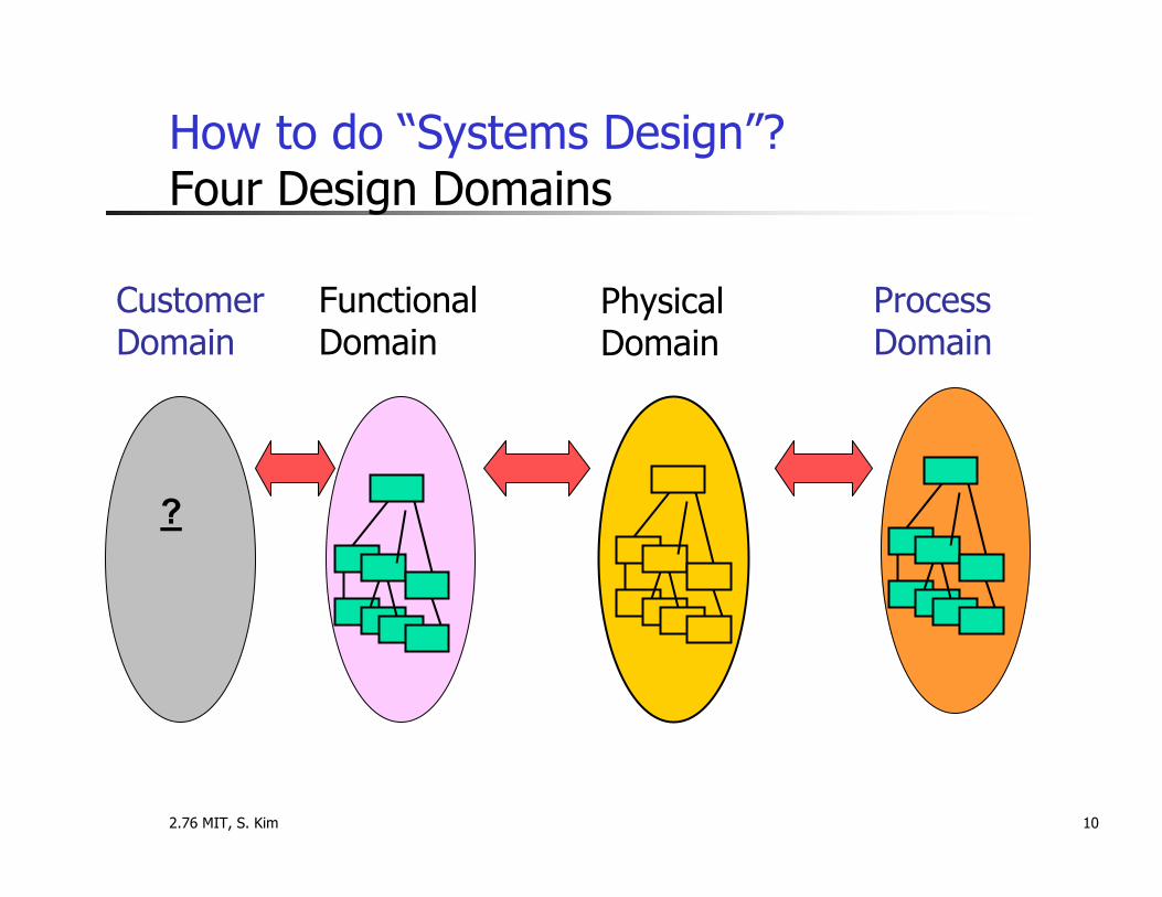
How to do “Systems Design”? Four Design Domains
CustomerDomain
FunctionalDomain
Physical Domain
ProcessDomain
?

2.76 MIT, S. Kim 11
Four domains
People resources
Programs offices
FunctionsCustomer satisfaction
Organization
ResourcesBusiness structure
Business goals
ROIBusiness
SubroutinesInput variables
Output of programs
Attributesdesired
Software
ProcessesMicro-structure
PropertiesPerformancesMaterials
PVDPFRCAManufacturingsystems

2.76 MIT, S. Kim 12
A multiscale design should be…
Customer’s needs Functionalities Design
parametersProcessvariables
MEMSMEMSOptics, BioOptics, Bio
Automobiles, Computers, TVs, Tools, ..
NanoNano--products?products?
m
µm
nmComplexityComplexity
Functionality Manufacturability
Chips

2.76 MIT, S. Kim 13
Customer SatisfactionConcurrent DesignDesign for Manufacturing, Assembly and “X”Quality Control, Six SigmaHouse of Quality, Takuchi methodAxiomatic Design
Systems Design
• Any of these efforts in MEMS?
• Nanomanufacturing, Complexity
Market
+ spiral
- spiral
Manufacturing
Manufacturing
Design
Market
Design

2.76 MIT, S. Kim 14
A Good Design is,
Axiomatic Design, 2.8821. N.P. Suh, Principles of Design, Oxford, 19902. N. P. Suh, Axiomatic Design: Advances and
Applications, Oxford, 20013. N. P. Suh, Complexity: Theory and Applications,
Oxford, 2004
Concept of Domains, well defined “what”Uncoupled (decoupled) Minimum information (least complex)

2.76 MIT, S. Kim 15
Example: Shower Faucet
Functional Requirements- Temperature- Flow rate
Figure by MIT OCW.

2.76 MIT, S. Kim 16
Independence Axiom
Maintain the independence of FRs.Shower faucet example
FR1FR2
DP1DP2
= X XX X
FR1= TemperatureFR2= Flow rate
DP1= Hot waterDP2= Cold Water
FR1FR2
DP1DP2
= X OO X
FR1= TemperatureFR2= Flow rate
DP1= Horizontal AngleDP2= Vertical Angle
Coupled Uncoupled

2.76 MIT, S. Kim 17
Design Coupling
Uncoupled
Decoupled
Coupled
FR1FR2
DP1DP2
= X OX X
FR1FR2
DP1DP2
= X OO X

2.76 MIT, S. Kim 18
Example: Xerography-based Printing Machine
Sele nium-coate dAlu mi numcylinder
WiperRoll
Originalima ge
Light
To nercontainer
Pape r-Fee dRoll
Image iscrea tedhere
Toner is c oatedon s urfa ces ofSelen iu m withelectric charges
Pape r
Courtesy of Prof. N. P. Suh. Used with permission.

2.76 MIT, S. Kim 19
Design Matrix
FR1 = Create electrically charged images.
FR2 = Coat the charged surface with toner
FR3 = Wipe off the excess toner.FR4 = Make sure that abrasive particles do not cause abrasion.FR5 = Feed the paper.FR6 = Transfer the toner to the paper.FR7 = Control throughput rate.
DP1 = Optical system with light on selenium surfaceDP2 = Electrostatic charges of the selenium surface and the tonerDP3 = Wiper rollerDP4 = Filter
DP5 = Paper-feeding mechanismDP6 = Mechanical pressureDP7 = Speed of the cylinder

2.76 MIT, S. Kim 20
Design Matrix
DP1
DP2
DP3
DP4
DP5
DP6
DP7
FR1
X 0 0 0 0 0 0
FR2
X X 0 0 0 0 0
FR3
0 0 X 0 0 0 0
FR4
0 0 X X X 0 0
FR5
0 0 0 0 X 0 0
FR6
0 0 0 0 0 X 0
FR7
0 0 0 0 X 0 X

2.76 MIT, S. Kim 21
Imaginary Complexity
FR1FR2FR3.........FRm
⎧
⎨
⎪ ⎪ ⎪ ⎪
⎩
⎪ ⎪ ⎪ ⎪
⎫
⎬
⎪ ⎪ ⎪ ⎪
⎭
⎪ ⎪ ⎪ ⎪
=
X 0 0 0 ... 0X X 0 0 ... 0X X X 0 ... 0... ... ... ... ... 0... ... ... ... ... 0... ... ... ... ... 0X X X X ... X
⎡
⎣
⎢ ⎢ ⎢ ⎢ ⎢ ⎢ ⎢ ⎢ ⎢
⎤
⎦
⎥ ⎥ ⎥ ⎥ ⎥ ⎥ ⎥ ⎥ ⎥
DP1DP2DP3............DPn
⎧
⎨
⎪ ⎪ ⎪ ⎪
⎩
⎪ ⎪ ⎪ ⎪
⎫
⎬
⎪ ⎪ ⎪ ⎪
⎭
⎪ ⎪ ⎪ ⎪
P =1n!

2.76 MIT, S. Kim 22
Solution
Vortexmoti on
Final tonerthi ckn es s
Main cylind erwith se leniumcoa ting
Wiperroller
DP41 = The order of rotation of the wiper roller and the main cylinder (wiper roller rotates first)DP42 = The surface speed of the wiper roller greater than and opposite to the surface speed of the main cylinder
Courtesy of Prof. N. P. Suh. Used with permission.

2.76 MIT, S. Kim 23
TMA(thinfilm micromirror array)
Mirror Array on
Piezoelectric
Actuator Array
Daewoo Electronics
Case study
Diagrams removed for copyright reasons.See S. G. Kim and Kyu-Ho Hwang, "Thin-film Micromirror Array", Information Display (Official Magazine of Society of Information Display, invited), Vol. 15, No. 4/5, pp.30-34, 1999.

2.76 MIT, S. Kim 24
Functional Requirements of TMA
1st GenerationFR1= light reflectionFR2= mirror tilting
DP1= cantilever top surfaceDP2= PZT sandwich
FR1FR2
DP1DP2
= X XX X

2.76 MIT, S. Kim 25
Functional Requirements of TMA
2nd GenerationFR1= light reflectionFR2= mirror tilting
DP1= cantilever top surfaceDP2= PZT sandwich
FR1
FR2
DP1
DP2
= X OX X

2.76 MIT, S. Kim 26
Functional Requirements of TMA
3rd GenerationFR1= light reflectionFR2= mirror tilting
DP1= cantilever top surfaceDP2= PZT sandwich
FR1
FR2
DP1
DP2
= X OO X

2.76 MIT, S. Kim 27
VGA640 X 480307,200 pixels
XGA1024 X 768
786,432 pixels
TMA
Photos removedfor copyright reasons.
Photos removedfor copyright reasons.

2.76 MIT, S. Kim 28
Information Axiom
Minimize the Information ContentPlog
P1logI 22 −==
P : Probability of success =common range/system range
System rangeDesign range
Common range
Prob
abili
ty d
ensi
ty
FR
bias

2.76 MIT, S. Kim 29
Multi-scale System Complexity
MIT Stata Center by Gehry
$300 million, 5years
DNA~2-1/2 nm diameter
MIT Simmons Hall$ 90million, 2 years
Carbon nanotube~2 nm diameter
natural
manmade
Nanotube transistor
Human heart
Human body(circulatory
system)Diagrams removedfor copyright reasons.

2.76 MIT, S. Kim 30
Scale Orders
• Cars: 5 m 500 µ • Jig Machines: 5 m 5 µ• Lithography M/C: 30 cm 30 nm• Human Body: 2 m 2 nm
• Scale order vs. Complexity?
Scale order, N = size of the systemsmallest characteristic length
N
104
106
107
109

2.76 MIT, S. Kim 31
Complexity of social problems
Uncertainty
Difficulty
Complexity

2.76 MIT, S. Kim 32
Non-equilibrium systems, long term stability
Pro babili tyDe n s i t y
FR
De si g nRa n g e
The S y ste m Ra n g e ch a ng es o ver t h ec o u rse o f the syste m’ s li fe.
Ti me
Courtesy of Prof. N. P. Suh. Used with permission.
2.76 MIT, S. Kim 33
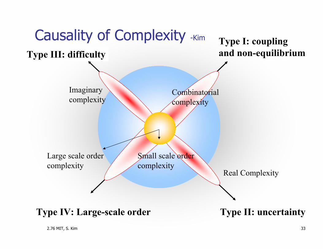
Causality of Complexity -Kim Type I: couplingand non-equilibrium
Type II: uncertainty
Type III: difficulty
Type IV: Large-scale order
Real Complexity
Imaginary complexity
Combinatorialcomplexity
Large scale order complexity
Small scale ordercomplexity

2.76 MIT, S. Kim 34
Real Complexity and the Scale Issue
the ratio (range/tolerance)
I = log( rangetolerance
)
tolerancerangeeI tolerance
range
== )(log
Suh
Kim

2.76 MIT, S. Kim 35
Nano-Scale Assembly
10 cm
100nm Carbon Nanotube100nm spacing
Three photos removed for copyright reasons.Force microscopy tip and two nanotube arrays.
2.76 MIT, S. Kim 36
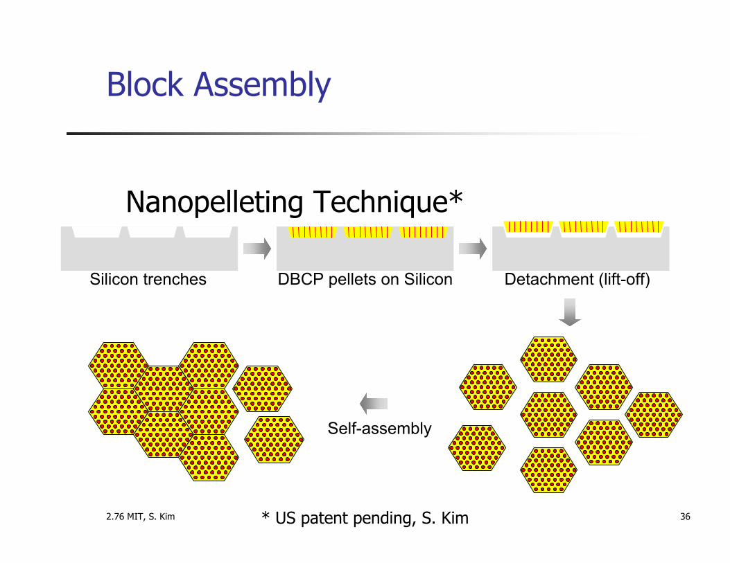
Block Assembly
Nanopelleting Technique*
Silicon trenches DBCP pellets on Silicon Detachment (lift-off)
Self-assembly
* US patent pending, S. Kim

2.76 MIT, S. Kim 37
Gordon Moore (Intel)
Two graphs of “Moore’s Laws” - removedfor copyright reasons.

2.76 MIT, S. Kim 38
Moore’s Second Law
The cost of building chip fabrication plants will continue to increase (and the return on investment to decrease) until it becomes fiscally untenable to build new plants.

2.76 MIT, S. Kim 39
Lithography Tool Cost
Year
Expo
sure
tool
pric
e
1980
Historical tool prices
300-mm 193-nm &
157-nm tools
$0
$5,000,000
$10,000,000
$15,000,000
$20,000,000
$25,000,000
$30,000,000
1985 1990 1995 2000 2005
{{
Figure by MIT OCW, after International Sematech.
2.76 MIT, S. Kim 40
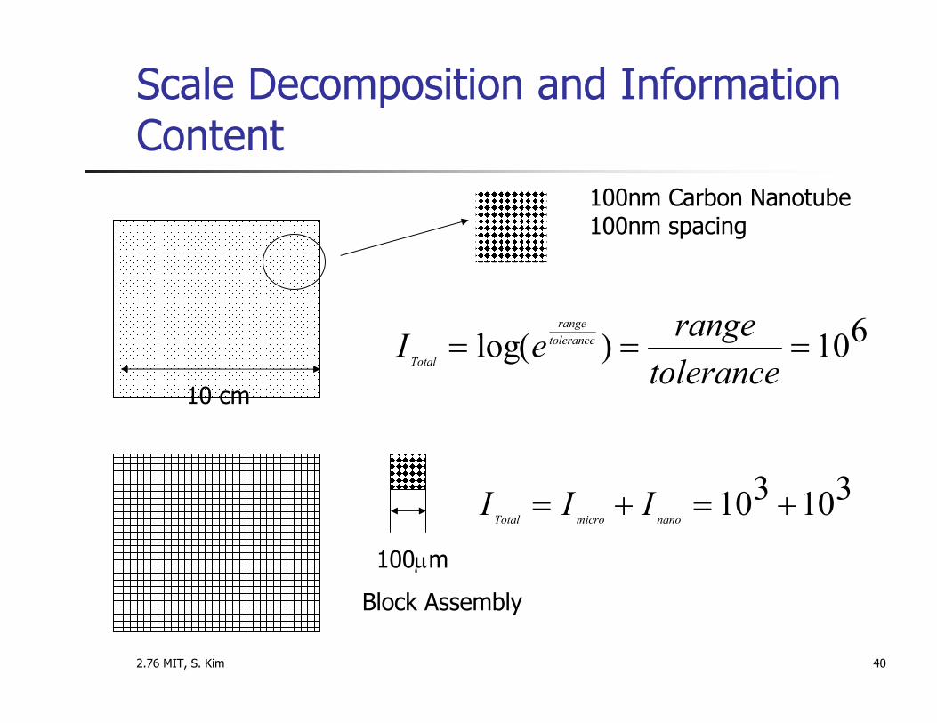
Scale Decomposition and Information Content
10 cm
100nm Carbon Nanotube100nm spacing
610)(log ===tolerancerangeeI tolerance
range
Total
100µm
Block Assembly
310310 +=+=nanomicroTotalIII

Sang-Gook Kim2.76 MIT, S. Kim
Complexity
A system is complex when;A design is strongly coupled or path-dependent,System ranges vary with time, (non-equilibrium)The outcome is uncertain, (low probability of success)The scale order is very high.
Complexity can be reduced by;Periodic Functions (temporal, spatial, etc.)Uncoupled

Sang-Gook Kim2.76 MIT, S. Kim
Functional Periodicity
Time independent real and imaginary complexity.Time dependent combinatorial and periodic complexity.Time dependent combinatorial complexity can become periodic complexity by functional periodicity. [Suh, MIT]
Temporal Geometrical Biological Manufacturing processChemical informationCircadianetc.

2.76 MIT, S. Kim 43
Functional Periodicities
Temporal periodicityGeometric periodicityBiological periodicityManufacturing process periodicityChemical periodicityThermal periodicityInformation process periodicityElectrical periodicityCircadian periodicityMaterial periodicity

2.76 MIT, S. Kim 44
Di-block copolymers
02BX
G∆2<
∂
∂
mmm ST∆H∆G ∆−=
Diagrams removed for copyright reasons.See C.T. Black, et al., Applied Physics Letters 79, 409, 2001.

2.76 MIT, S. Kim 45
Micro-phase Separation
Random walk, Gaussian distribution
e-to-e distance, R = aN1/2
Rg = aN1/2/6N: number of monomers
Micro-domain periodicity, L
21
g aNRL ∝∝
N=1,000a=5 angstromsThen, L is around 15 nm.

2.76 MIT, S. Kim 46
Multi-scale system assembly by periodic building blocks?
Periodic micro-domainsFunctionally uncoupled domainsPeriodicity, CNT assembly
MIT Simmons Hall
21
g aNRL ∝∝

2.76 MIT, S. Kim Sang-Gook Kim
Inter-layer Nanopellets
for Composites1
1-20 microns
Single strand
bundle
1. Wardle and Kim, US patent pending

2.76 MIT, S. Kim S.G. KIM, MIT
Multi-scale Manufacturing at Kim’s Group
+ - + -+ - +E3
The
Mic
row
orld
0.1 nm
1 nanometer (nm)
0.01 µm10 nm
0.1 µm100 nm
1 micrometer (µm)
0.01 mm10 µm
0.1 mm100 µm
1 millimeter (mm)
1 cm10 mm10-2 m
10-3 m
10-4 m
10-5 m
10-6 m
10-7 m
10-8 m
10-9 m
10-10 m
Visib
le
The
Nan
owor
ld
1,000 nanometers =
Infra
red
Ultra
violet
Micr
owav
eSo
ft x-
ray
1,000,000 nanometers =
Things Natural Energy Harvesting
RF Switch
TunablePhotonics
Nanopipette
airsubstrate
PMMA on Sia d
Things Engineered
DNAproteins nm
Molecule,Atoms
bacteria1 µm
red blood cell~5 µm
Human hair~ 10-50 mm wide
Human heart
Diagrams removedfor copyright reasons.


