2
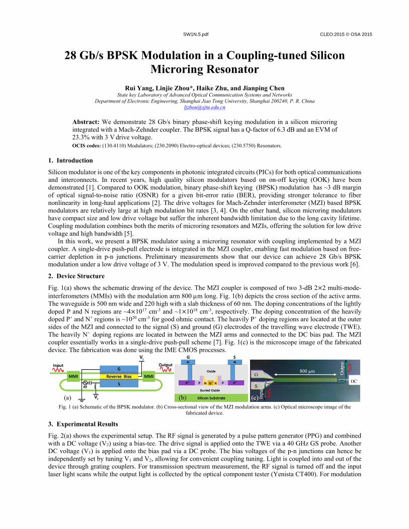
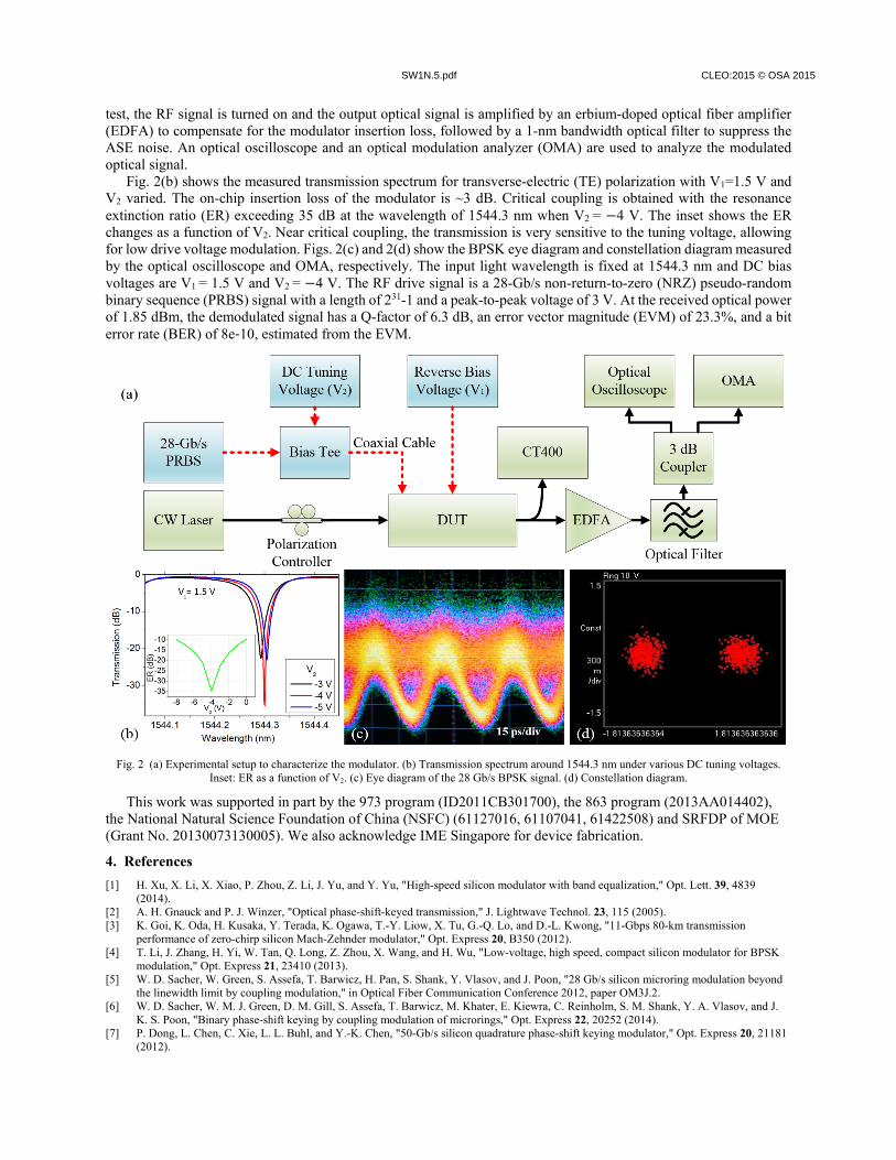
SW1N.5.pdf CLEO:2015 © OSA 2015 28 Gb/s BPSK Modulation in a Coupling-tuned Silicon Microring Resonator Rui Yang, Linjie Zhou*, Haike Zhu, and Jianping Chen State key Laboratory of Advanced Optical Communication Systems and Networks Department of Electronic Engineering, Shanghai Jiao Tong University, Shanghai 200240, P. R. China [email protected] Abstract: We demonstrate 28 Gb/s binary phase-shift keying modulation in a silicon microring integrated with a Mach-Zehnder coupler. The BPSK signal has a Q-factor of 6.3 dB and an EVM of 23.3% with 3 V drive voltage. OCIS codes: (130.4110) Modulators; (230.2090) Electro-optical devices; (230.5750) Resonators. 1. Introduction Silicon modulator is one of the key components in photonic integrated circuits (PICs) for both optical communications and interconnects. In recent years, high quality silicon modulators based on on-off keying (OOK) have been demonstrated [1]. Compared to OOK modulation, binary phase-shift keying (BPSK) modulation has ~3 dB margin of optical signal-to-noise ratio (OSNR) for a given bit-error ratio (BER), providing stronger tolerance to fiber nonlinearity in long-haul applications [2]. The drive voltages for Mach-Zehnder interferometer (MZI) based BPSK modulators are relatively large at high modulation bit rates [3, 4]. On the other hand, silicon microring modulators have compact size and low drive voltage but suffer the inherent bandwidth limitation due to the long cavity lifetime. Coupling modulation combines both the merits of microring resonators and MZIs, offering the solution for low drive voltage and high bandwidth [5]. In this work, we present a BPSK modulator using a microring resonator with coupling implemented by a MZI coupler. A single-drive push-pull electrode is integrated in the MZI coupler, enabling fast modulation based on free- carrier depletion in p-n junctions. Preliminary measurements show that our device can achieve 28 Gb/s BPSK modulation under a low drive voltage of 3 V. The modulation speed is improved compared to the previous work [6]. 2. Device Structure Fig. 1(a) shows the schematic drawing of the device. The MZI coupler is composed of two 3-dB 2×2 multi-mode- interferometers (MMIs) with the modulation arm 800 µm long. Fig. 1(b) depicts the cross section of the active arms. The waveguide is 500 nm wide and 220 high with a slab thickness of 60 nm. The doping concentrations of the lightly doped P and N regions are ~4×10 17 cm -3 and ~1×10 18 cm -3 , respectively. The doping concentration of the heavily doped P + and N + regions is ~10 20 cm -3 for good ohmic contact. The heavily P + doping regions are located at the outer sides of the MZI and connected to the signal (S) and ground (G) electrodes of the travelling wave electrode (TWE). The heavily N + doping regions are located in between the MZI arms and connected to the DC bias pad. The MZI coupler essentially works in a single-drive push-pull scheme [7]. Fig. 1(c) is the microscope image of the fabricated device. The fabrication was done using the IME CMOS processes. Fig. 1 (a) Schematic of the BPSK modulator. (b) Cross-sectional view of the MZI modulation arms. (c) Optical microscope image of the fabricated device. 3. Experimental Results Fig. 2(a) shows the experimental setup. The RF signal is generated by a pulse pattern generator (PPG) and combined with a DC voltage (V 2 ) using a bias-tee. The drive signal is applied onto the TWE via a 40 GHz GS probe. Another DC voltage (V 1 ) is applied onto the bias pad via a DC probe. The bias voltages of the p-n junctions can hence be independently set by tuning V 1 and V 2 , allowing for convenient coupling tuning. Light is coupled into and out of the device through grating couplers. For transmission spectrum measurement, the RF signal is turned off and the input laser light scans while the output light is collected by the optical component tester (Yenista CT400). For modulation