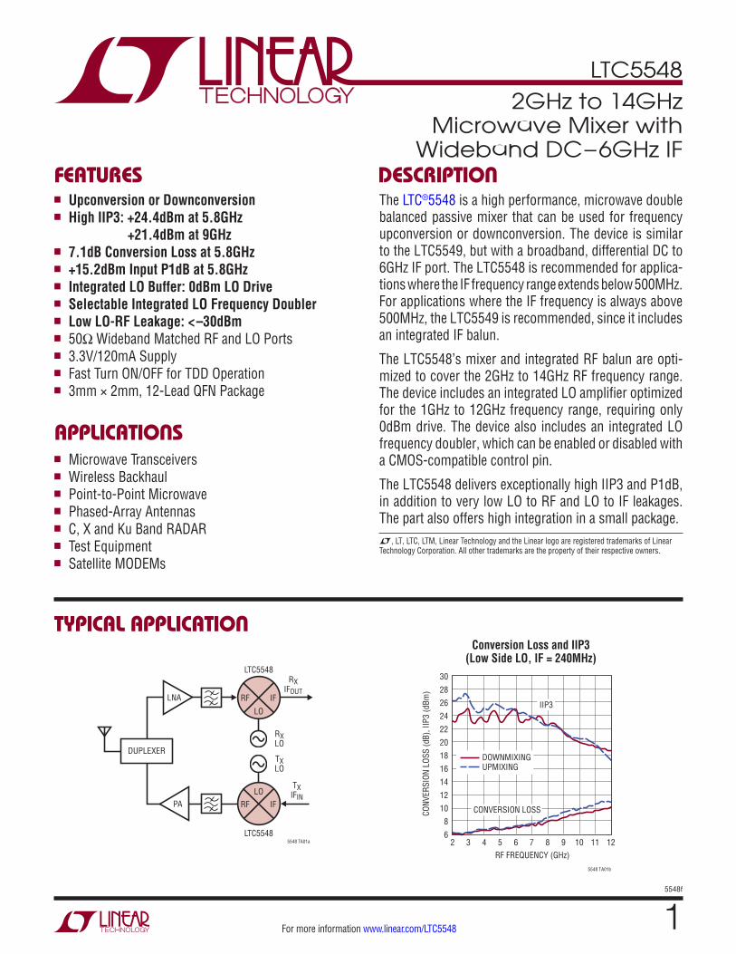
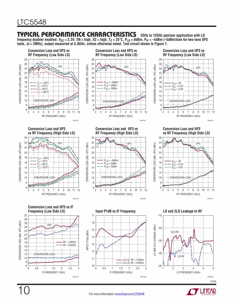
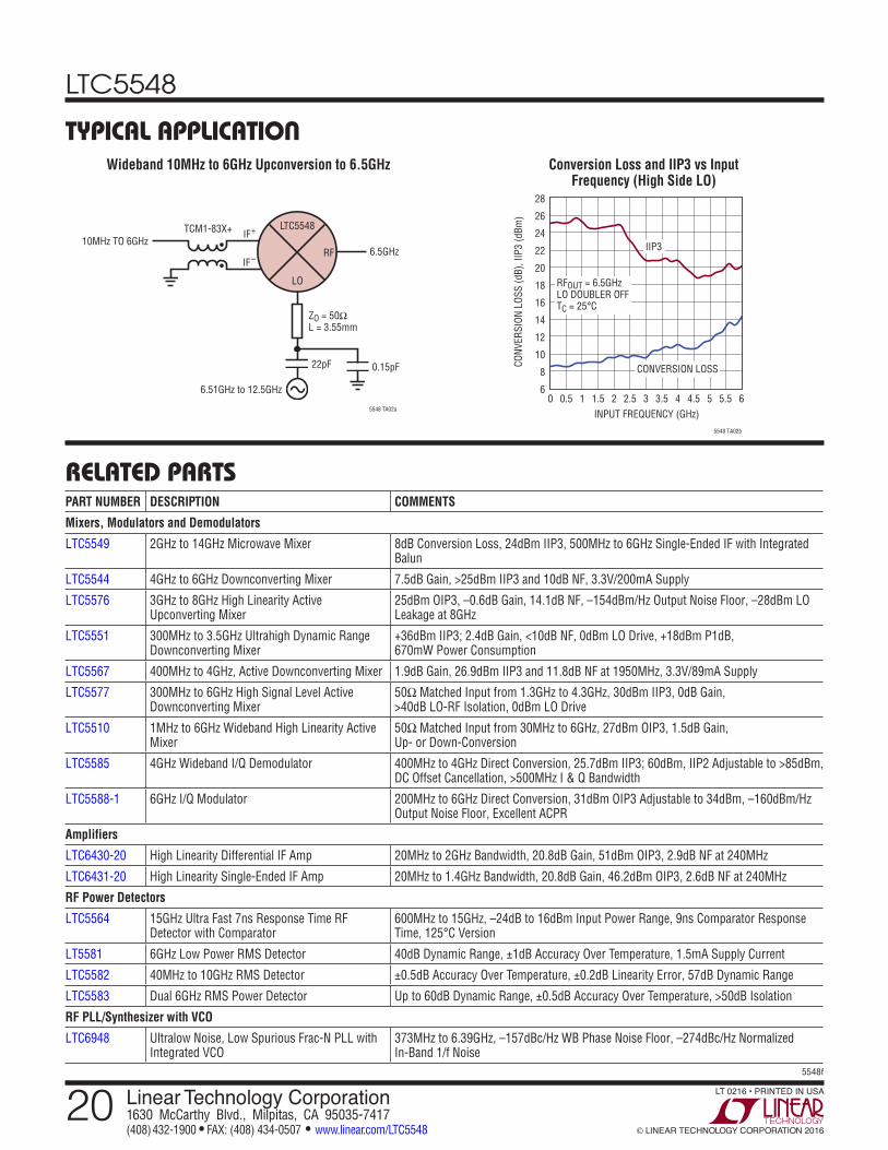
LTC5548 1 5548f For more information www.linear.com/LTC5548 TYPICAL APPLICATION FEATURES DESCRIPTION 2GHz to 14GHz Microwave Mixer with Wideband DC–6GHz IF The LTC ® 5548 is a high performance, microwave double balanced passive mixer that can be used for frequency upconversion or downconversion. The device is similar to the LTC5549, but with a broadband, differential DC to 6GHz IF port. The LTC5548 is recommended for applica- tions where the IF frequency range extends below 500MHz. For applications where the IF frequency is always above 500MHz, the LTC5549 is recommended, since it includes an integrated IF balun. The LTC5548’s mixer and integrated RF balun are opti- mized to cover the 2GHz to 14GHz RF frequency range. The device includes an integrated LO amplifier optimized for the 1GHz to 12GHz frequency range, requiring only 0dBm drive. The device also includes an integrated LO frequency doubler, which can be enabled or disabled with a CMOS-compatible control pin. The LTC5548 delivers exceptionally high IIP3 and P1dB, in addition to very low LO to RF and LO to IF leakages. The part also offers high integration in a small package. Conversion Loss and IIP3 (Low Side LO, IF = 240MHz) APPLICATIONS n Upconversion or Downconversion n High IIP3: +24.4dBm at 5.8GHz +21.4dBm at 9GHz n 7.1dB Conversion Loss at 5.8GHz n +15.2dBm Input P1dB at 5.8GHz n Integrated LO Buffer: 0dBm LO Drive n Selectable Integrated LO Frequency Doubler n Low LO-RF Leakage: < –30dBm n 50Ω Wideband Matched RF and LO Ports n 3.3V/120mA Supply n Fast Turn ON/OFF for TDD Operation n 3mm × 2mm, 12-Lead QFN Package n Microwave Transceivers n Wireless Backhaul n Point-to-Point Microwave n Phased-Array Antennas n C, X and Ku Band RADAR n Test Equipment n Satellite MODEMs L, LT, LTC, LTM, Linear Technology and the Linear logo are registered trademarks of Linear Technology Corporation. All other trademarks are the property of their respective owners. DUPLEXER LNA PA LTC5548 R X IF OUT T X IF IN R X LO T X LO LO RF IF LTC5548 LO RF IF 5548 TA01a RF FREQUENCY (GHz) 2 CONVERSION LOSS (dB), IIP3 (dBm) 14 18 12 5548 TA01b 10 6 4 6 8 3 5 7 9 10 11 30 12 16 22 26 20 24 8 28 IIP3 CONVERSION LOSS DOWNMIXING UPMIXING
Transcript
LTC5548
15548f
For more information www.linear.com/LTC5548
Typical applicaTion
FeaTures DescripTion
2GHz to 14GHz Microwave Mixer with
Wideband DC–6GHz IF
The LTC®5548 is a high performance, microwave double balanced passive mixer that can be used for frequency upconversion or downconversion. The device is similar to the LTC5549, but with a broadband, differential DC to 6GHz IF port. The LTC5548 is recommended for applica-tions where the IF frequency range extends below 500MHz. For applications where the IF frequency is always above 500MHz, the LTC5549 is recommended, since it includes an integrated IF balun.
The LTC5548’s mixer and integrated RF balun are opti-mized to cover the 2GHz to 14GHz RF frequency range. The device includes an integrated LO amplifier optimized for the 1GHz to 12GHz frequency range, requiring only 0dBm drive. The device also includes an integrated LO frequency doubler, which can be enabled or disabled with a CMOS-compatible control pin.
The LTC5548 delivers exceptionally high IIP3 and P1dB, in addition to very low LO to RF and LO to IF leakages. The part also offers high integration in a small package.
Conversion Loss and IIP3(Low Side LO, IF = 240MHz)
applicaTions
n Upconversion or Downconversion n High IIP3: +24.4dBm at 5.8GHz
+21.4dBm at 9GHz n 7.1dB Conversion Loss at 5.8GHz n +15.2dBm Input P1dB at 5.8GHz n Integrated LO Buffer: 0dBm LO Drive n Selectable Integrated LO Frequency Doubler n Low LO-RF Leakage: <–30dBm n 50Ω Wideband Matched RF and LO Ports n 3.3V/120mA Supply n Fast Turn ON/OFF for TDD Operation n 3mm × 2mm, 12-Lead QFN Package
n Microwave Transceivers n Wireless Backhaul n Point-to-Point Microwave n Phased-Array Antennas n C, X and Ku Band RADAR n Test Equipment n Satellite MODEMs
L, LT, LTC, LTM, Linear Technology and the Linear logo are registered trademarks of Linear Technology Corporation. All other trademarks are the property of their respective owners.
Supply Voltage (VCC) ..................................................4VEnable Input Voltage (EN) ................–0.3V to VCC + 0.3VX2 Input Voltage (X2) ......................–0.3V to VCC + 0.3VLO Input Power (1GHz to 12GHz) .................. ….+10dBmLO Input DC Voltage ............................................ ±0.1VRF Power (2GHz to 14GHz) ................................+20dBmRF DC Voltage ....................................................... ±0.1VIF+/IF– Input Power (LF to 6GHz) .......................+20dBmIF+/IF– Input DC Voltage .........................................±0.3VOperating Temperature Range (TC) ........ –40°C to 105°CStorage Temperature Range .................. –65°C to 150°CJunction Temperature (TJ) .................................... 150°C
(Note 1)
VCC
X2
EN
9
8
7
GND
IF+
IF–
1
2
3
13GND
GND RF
GND
4 5 6
GND
LO GND
12 11 10
TOP VIEW
UDB PACKAGE12-LEAD (3mm × 2mm) PLASTIC QFN
TJMAX = 150°C, θJC = 25°C/W EXPOSED PAD (PIN 13) IS GND, MUST BE SOLDERED TO PCB
orDer inForMaTion
PARAMETER CONDITIONS MIN TYP MAX UNITS
Power Supply Requirements
Supply Voltage (VCC) l 3.0 3.3 3.6 V
Supply Current Enabled X2 = Low (LO Doubler Off) X2 = High (LO Doubler On)
120 136
140 160
mA mA
Shutdown Current EN = Low 100 μA
Enable (EN) and LO Frequency Doubler (X2) Logic Inputs
Input High Voltage (On) l 1.2 V
Input Low Voltage (Off) l 0.3 V
Input Current –0.3V to VCC + 0.3V –30 100 μA
Chip Turn-On Time 0.2 μs
Chip Turn-Off Time 0.1 μs
Dc elecTrical characTerisTics The l denotes the specifications which apply over the full operating temperature range, otherwise specifications are at TC = 25°C. VCC = 3.3V, EN = High, unless otherwise noted. Test circuit shown in Figure 1. (Note 2)
Lead Free FinishTAPE AND REEL (MINI) TAPE AND REEL PART MARKING PACKAGE DESCRIPTION TEMPERATURE RANGE
LTC5548IUDB#TRMPBF LTC5548IUDB#TRPBF LGXF 12-Lead (3mm × 2mm) Plastic QFN –40°C to 105°CTRM = 500 pieces.Consult LTC Marketing for parts specified with wider operating temperature ranges.For more information on lead free part marking, go to: http://www.linear.com/leadfree/ For more information on tape and reel specifications, go to: http://www.linear.com/tapeandreel/. Some packages are available in 500 unit reels through designated sales channels with #TRMPBF suffix.
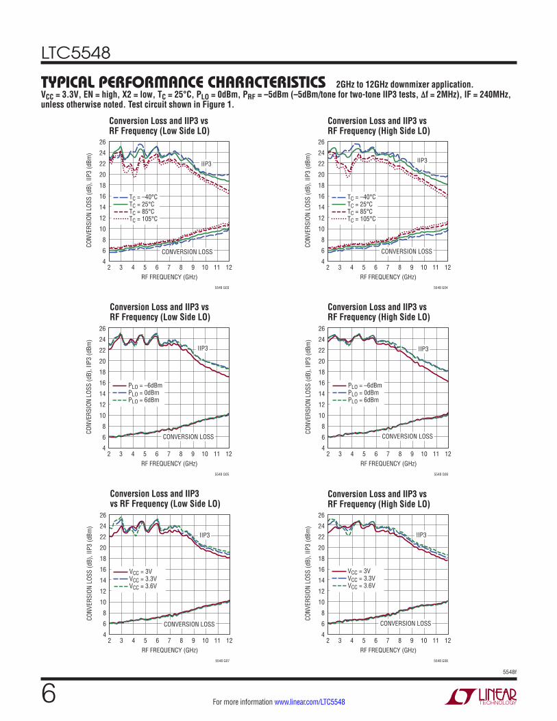
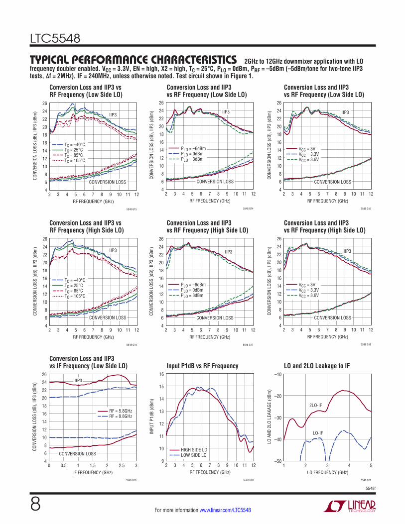
ac elecTrical characTerisTics The l denotes the specifications which apply over the full operating temperature range, otherwise specifications are at TC = 25°C. VCC = 3.3V, EN = High, PLO = 0dBm, PRF = –5dBm (–5dBm/tone for two-tone IIP3 tests), unless otherwise noted. Test circuit shown in Figure 1. (Notes 2, 3)
PARAMETER CONDITIONS MIN TYP MAX UNITS
LO Frequency Range l 1 to 12 GHz
RF Frequency Range l 2 to 14 GHz
IF Frequency Range l DC to 6000 MHz
RF Return Loss ZO = 50Ω, 2GHz to 13.6GHz >9 dB
LO Input Return Loss ZO = 50Ω, 1GHz to 12GHz >10 dB
LO Input Power X2 = Low X2 = High
–6 –6
0 0
6 3
dBm dBm
Downmixer Application with LO Doubler Off (X2 = Low), IF = 240MHz, Low Side LO
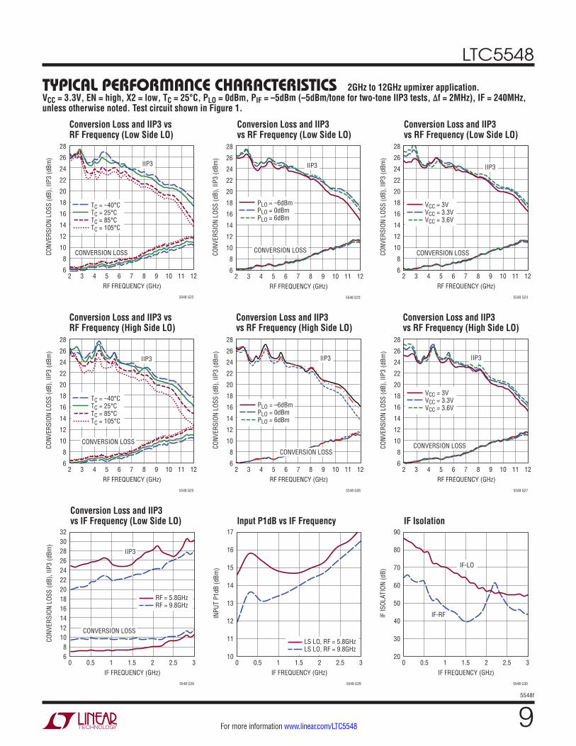
ac elecTrical characTerisTics The l denotes the specifications which apply over the full operating temperature range, otherwise specifications are at TC = 25°C. VCC = 3.3V, EN = High, PLO = 0dBm, PIF = –5dBm (–5dBm/tone for two-tone IIP3 tests), unless otherwise noted. Test circuit shown in Figure 1. (Notes 2, 3)
PARAMETER CONDITIONS MIN TYP MAX UNITS
Upmixer Application with LO Doubler Off (X2 = Low), IF = 240MHz, Low Side LO
LO to RF Output Leakage fLO = 1GHz to 5GHz <–30 dBm
2LO to RF Output Leakage fLO = 1GHz to 5GHz <–25 dBm
LO to IF Input Leakage fLO = 1GHz to 5GHz <–36 dBm
2LO to IF Input Leakage fLO = 1GHz to 5GHz <–20 dBm
Input 1dB Compression RF Output = 5.8GHz 14.8 dBm
Note 1: Stresses beyond those listed under Absolute Maximum Ratings may cause permanent damage to the device. Exposure to any Absolute Maximum Rating condition for extended periods may affect device reliability and lifetime.Note 2: The LTC5548 is guaranteed functional over the –40°C to 105°C case temperature range (θJC = 25°C/W).
Note 3: SSB noise figure measurements performed with a small-signal noise source, bandpass filter and 2dB matching pad on input, with bandpass filters on LO, and output.
pin FuncTionsGND (Pins 1, 4, 6, 10, 12, Exposed Pad Pin 13): Ground. These pins must be soldered to the RF ground on the circuit board. The exposed pad metal of the package provides both electrical contact to ground and good thermal contact to the printed circuit board.
IF+, IF– (Pins 2, 3): Differential Terminals for the IF. These pins may be used for a differential IF or connected to an external balun if a single-ended IF port is needed. The IF port can be used from DC up to 6GHz depending on the external balun bandwidth.
RF (Pin 5): Single-Ended Terminal for the RF Port. This pin is internally connected to the primary side of the RF transformer, which has low DC resistance to ground. A series DC blocking capacitor must be used to avoid damage to the integrated transformer if DC voltage is present. The RF port is impedance matched from 2GHz to 14GHz as long as the LO is driven with a 0 ±6dBm source between 1GHz and 12GHz.
EN (Pin 7): Enable Pin. When the voltage applied to this pin is greater than 1.2V, the mixer is enabled. When the voltage is less than 0.3V, the mixer is disabled. Typical input current is less than 30μA. This pin has an internal 376kΩ pull-down resistor.
X2 (Pin 8): Digital Control Pin for LO Frequency Doubler. When the voltage applied to this pin is greater than 1.2V, the LO frequency doubler is enabled. When the voltage DC is less than 0.3V, the LO frequency doubler is disabled. Typical input current is less than 30μA. This pin has an internal 376kΩ pull-down resistor.
VCC (Pin 9): Power Supply Pin. This pin must be externally connected to a regulated 3.3V supply, with a bypass capaci-tor located close to the pin. Typical current consumption is 120mA when the part is enabled.
LO (Pin 11): Input for the Local Oscillator (LO). A series DC blocking capacitor must be used. Typical DC voltage at this pin is 1.6V.
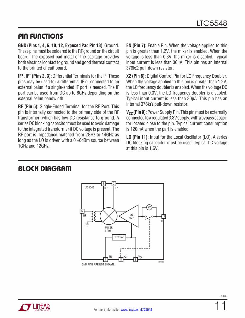
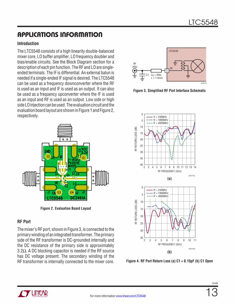
The LTC5548 consists of a high linearity double-balanced mixer core, LO buffer amplifier, LO frequency doubler and bias/enable circuits. See the Block Diagram section for a description of each pin function. The RF and LO are single-ended terminals. The IF is differential. An external balun is needed if a single-ended IF signal is desired. The LTC5548 can be used as a frequency downconverter where the RF is used as an input and IF is used as an output. It can also be used as a frequency upconverter where the IF is used as an input and RF is used as an output. Low side or high side LO injection can be used. The evaluation circuit and the evaluation board layout are shown in Figure 1 and Figure 2, respectively.
Figure 2. Evaluation Board Layout
Figure 3. Simplified RF Port Interface Schematic
Figure 4. RF Port Return Loss (a) C1 = 0.15pF (b) C1 Open
(b)
(a)
RF Port
The mixer’s RF port, shown in Figure 3, is connected to the primary winding of an integrated transformer. The primary side of the RF transformer is DC-grounded internally and the DC resistance of the primary side is approximately 3.2Ω. A DC blocking capacitor is needed if the RF source has DC voltage present. The secondary winding of the RF transformer is internally connected to the mixer core.
The RF port is broadband matched to 50Ω from 2GHz to 14GHz with a 0.15pF shunt capacitor (C1) located 1.4mm away from the RF pin. The RF port is 50Ω matched from 2GHz to 10GHz without C1. An LO between –6dBm and 6dBm is required for good RF impedance matching. The measured RF input return loss is shown in Figure 4 for IF frequencies of 240MHz, 1890MHz and 4GHz with low side LO.
The RF input impedance and input reflection coefficient versus RF frequency is listed in Table 1. The reference plane for this data is Pin 5 of the IC, with no external matching, and the LO is driven at 7.5GHz.
Table 1. RF Input Impedance and S11 (at Pin 5, No External Matching, LO Input Driven at 7.5GHz)
FREQUENCY (GHz)
INPUT IMPEDANCE
S11
MAG ANGLE
2 34.3+j28.9 0.37 99.6
3 49.4+j24.7 0.24 77.4
4 57.2-j3.8 0.08 –25.8
5 37.7+j4.4 0.15 157.4
6 43.4+j2.2 0.07 160.2
7 46.2-j1.9 0.04 –152.3
8 47.8-j1.1 0.02 –155.0
Table 1. RF Input Impedance and S11 (at Pin 5, No External Matching, LO Input Driven at 7.5GHz)
9 48.8+j0.6 0.01 152.8
10 46.1+j9.1 0.10 107.8
11 35.8+j3.2 0.17 165.2
12 16.3+j4.1 0.51 169.5
13 10.9+j2.3 0.64 174.5
14 12.9-j3.5 0.59 –171.4
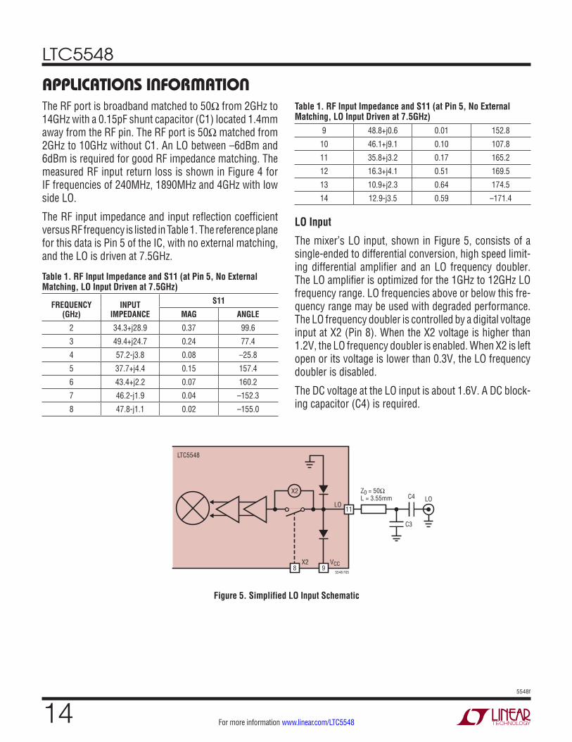
LO Input
The mixer’s LO input, shown in Figure 5, consists of a single-ended to differential conversion, high speed limit-ing differential amplifier and an LO frequency doubler. The LO amplifier is optimized for the 1GHz to 12GHz LO frequency range. LO frequencies above or below this fre-quency range may be used with degraded performance. The LO frequency doubler is controlled by a digital voltage input at X2 (Pin 8). When the X2 voltage is higher than 1.2V, the LO frequency doubler is enabled. When X2 is left open or its voltage is lower than 0.3V, the LO frequency doubler is disabled.
The DC voltage at the LO input is about 1.6V. A DC block-ing capacitor (C4) is required.
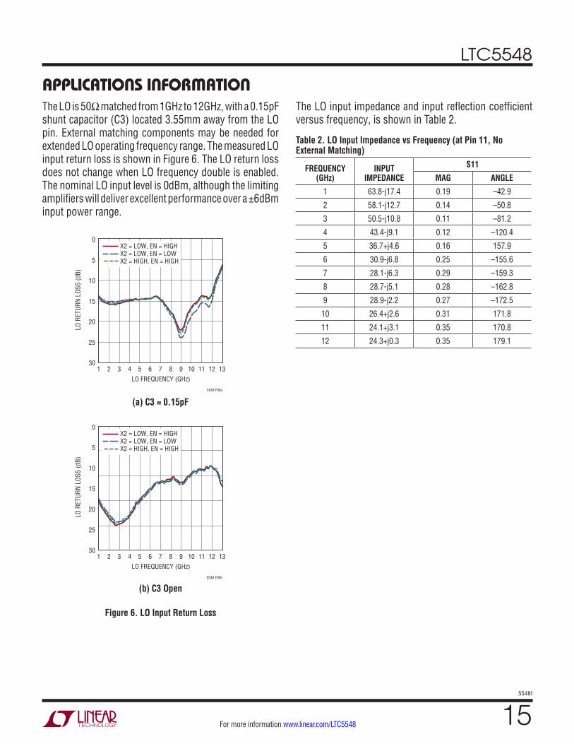
applicaTions inForMaTionThe LO is 50Ω matched from 1GHz to 12GHz, with a 0.15pF shunt capacitor (C3) located 3.55mm away from the LO pin. External matching components may be needed for extended LO operating frequency range. The measured LO input return loss is shown in Figure 6. The LO return loss does not change when LO frequency double is enabled. The nominal LO input level is 0dBm, although the limiting amplifiers will deliver excellent performance over a ±6dBm input power range.
LO FREQUENCY (GHz)1
LO R
ETUR
N LO
SS (d
B)
13
5548 F06a
303 5 72 4 6 8 10 119 12
0
20
10
25
15
5
X2 = LOW, EN = HIGHX2 = LOW, EN = LOWX2 = HIGH, EN = HIGH
LO FREQUENCY (GHz)1
LO R
ETUR
N LO
SS (d
B)
13
5548 F06b
303 5 72 4 6 8 10 119 12
0
20
10
25
15
5
X2 = LOW, EN = HIGHX2 = LOW, EN = LOWX2 = HIGH, EN = HIGH
(a) C3 = 0.15pF
(b) C3 Open
The LO input impedance and input reflection coefficient versus frequency, is shown in Table 2.
Table 2. LO Input Impedance vs Frequency (at Pin 11, No External Matching)
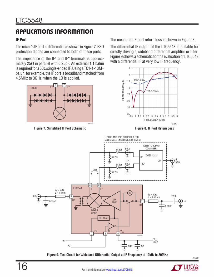
Figure 7. Simplified IF Port Schematic Figure 8. IF Port Return Loss
LTC5548 IF+IF–
5548 F07
3 2
applicaTions inForMaTionIF Port
The mixer’s IF port is differential as shown in Figure 7. ESD protection diodes are connected to both of these ports.
The impedance of the IF+ and IF– terminals is approxi-mately 25Ω in parallel with 0.25pF. An external 1:1 balun is required for a 50Ω single-ended IF. Using a TC1-1-13M+ balun, for example, the IF port is broadband matched from 4.5MHz to 3GHz, when the LO is applied.
The measured IF port return loss is shown in Figure 8.
The differential IF output of the LTC5548 is suitable for directly driving a wideband differential amplifier or filter. Figure 9 shows a schematic for the evaluation of LTC5548 with a differential IF at very low IF frequency.
Figure 9. Test Circuit for Wideband Differential Output at IF Frequency of 10kHz to 20MHz
5548 F09
LTC5548
RF
9
5
X2 VCCEN7
IF+IF–
LO
11
X2
23
LOAMP
MIXERCORE
8
REF/BIAS
Z0 = 50ΩL = 1.4mm
0.15pF
RFZ0 = 50ΩL = 3.55mm
0.15pF
22pF
LO
VCC3.3V
22pF 1µF
EN
X2
35.7Ω
34.8ΩIF–
50Ω
35.7Ω
34.8ΩIF+
50Ω
50Ω
L-PADS AND 180° COMBINER FOR50Ω SINGLE-ENDED MEASUREMENT
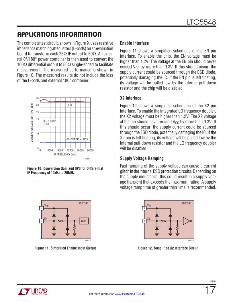
applicaTions inForMaTionThe complete test circuit, shown in Figure 9, uses resistive impedance matching attenuators (L-pads) on an evaluation board to transform each 25Ω IF output to 50Ω. An exter-nal 0°/180° power combiner is then used to convert the 100Ω differential output to 50Ω single-ended to facilitate measurement. The measured performance is shown in Figure 10. The measured results do not include the loss of the L-pads and external 180° combiner.
Enable Interface
Figure 11 shows a simplified schematic of the EN pin interface. To enable the chip, the EN voltage must be higher than 1.2V. The voltage at the EN pin should never exceed VCC by more than 0.3V. If this should occur, the supply current could be sourced through the ESD diode, potentially damaging the IC. If the EN pin is left floating, its voltage will be pulled low by the internal pull-down resistor and the chip will be disabled.
X2 Interface
Figure 12 shows a simplified schematic of the X2 pin interface. To enable the integrated LO frequency doubler, the X2 voltage must be higher than 1.2V. The X2 voltage at the pin should never exceed VCC by more than 0.3V. If this should occur, the supply current could be sourced through the ESD diode, potentially damaging the IC. If the X2 pin is left floating, its voltage will be pulled low by the internal pull-down resistor and the LO frequency doubler will be disabled.
Supply Voltage Ramping
Fast ramping of the supply voltage can cause a current glitch in the internal ESD protection circuits. Depending on the supply inductance, this could result in a supply volt-age transient that exceeds the maximum rating. A supply voltage ramp time of greater than 1ms is recommended.
Figure 10. Conversion Gain and IIP3 for Differential IF Frequency of 10kHz to 20MHz
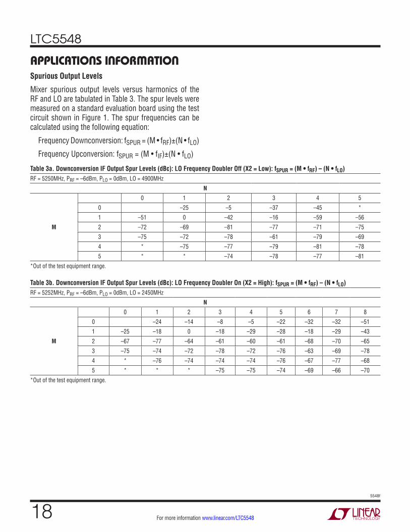
Mixer spurious output levels versus harmonics of the RF and LO are tabulated in Table 3. The spur levels were measured on a standard evaluation board using the test circuit shown in Figure 1. The spur frequencies can be calculated using the following equation:
Frequency Downconversion: fSPUR = (M • fRF)±(N • fLO)
Frequency Upconversion: fSPUR = (M • fIF)±(N • fLO)
Table 3a. Downconversion IF Output Spur Levels (dBc): LO Frequency Doubler Off (X2 = Low): fSPUR = (M • fRF) – (N • fLO)RF = 5250MHz, PRF = –6dBm, PLO = 0dBm, LO = 4900MHz
N
M
0 1 2 3 4 5
0 –25 –5 –37 –45 *
1 –51 0 –42 –16 –59 –56
2 –72 –69 –81 –77 –71 –75
3 –75 –72 –78 –61 –79 –69
4 * –75 –77 –79 –81 –78
5 * * –74 –78 –77 –81
*Out of the test equipment range.
Table 3b. Downconversion IF Output Spur Levels (dBc): LO Frequency Doubler On (X2 = High): fSPUR = (M • fRF) – (N • fLO)RF = 5252MHz, PRF = –6dBm, PLO = 0dBm, LO = 2450MHz
Information furnished by Linear Technology Corporation is believed to be accurate and reliable. However, no responsibility is assumed for its use. Linear Technology Corporation makes no representa-tion that the interconnection of its circuits as described herein will not infringe on existing patent rights.
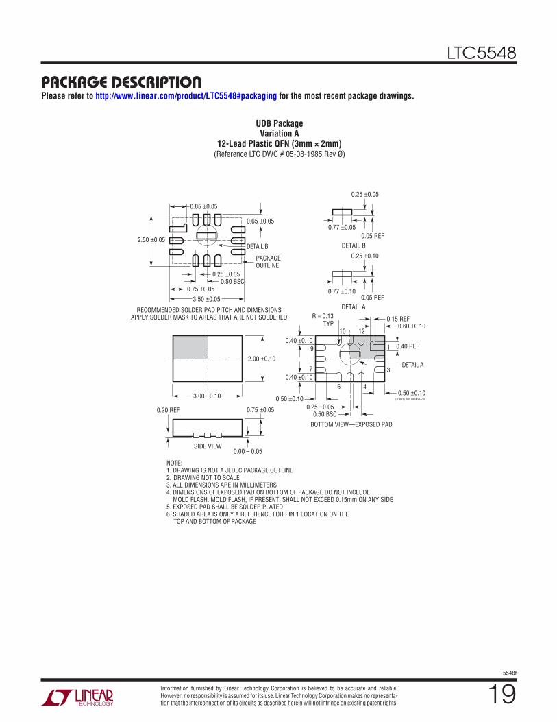
NOTE:1. DRAWING IS NOT A JEDEC PACKAGE OUTLINE 2. DRAWING NOT TO SCALE3. ALL DIMENSIONS ARE IN MILLIMETERS4. DIMENSIONS OF EXPOSED PAD ON BOTTOM OF PACKAGE DO NOT INCLUDE MOLD FLASH. MOLD FLASH, IF PRESENT, SHALL NOT EXCEED 0.15mm ON ANY SIDE5. EXPOSED PAD SHALL BE SOLDER PLATED 6. SHADED AREA IS ONLY A REFERENCE FOR PIN 1 LOCATION ON THE TOP AND BOTTOM OF PACKAGE
RECOMMENDED SOLDER PAD PITCH AND DIMENSIONSAPPLY SOLDER MASK TO AREAS THAT ARE NOT SOLDERED
For more information www.linear.com/LTC5548 LINEAR TECHNOLOGY CORPORATION 2016
LT 0216 • PRINTED IN USALinear Technology Corporation1630 McCarthy Blvd., Milpitas, CA 95035-7417(408) 432-1900 FAX: (408) 434-0507 www.linear.com/LTC5548
relaTeD parTs
Typical applicaTion
PART NUMBER DESCRIPTION COMMENTS
Mixers, Modulators and Demodulators
LTC5549 2GHz to 14GHz Microwave Mixer 8dB Conversion Loss, 24dBm IIP3, 500MHz to 6GHz Single-Ended IF with Integrated Balun
LTC5544 4GHz to 6GHz Downconverting Mixer 7.5dB Gain, >25dBm IIP3 and 10dB NF, 3.3V/200mA Supply
LTC5576 3GHz to 8GHz High Linearity Active Upconverting Mixer
25dBm OIP3, –0.6dB Gain, 14.1dB NF, –154dBm/Hz Output Noise Floor, –28dBm LO Leakage at 8GHz
LTC5551 300MHz to 3.5GHz Ultrahigh Dynamic Range Downconverting Mixer
+36dBm IIP3; 2.4dB Gain, <10dB NF, 0dBm LO Drive, +18dBm P1dB, 670mW Power Consumption
LTC5567 400MHz to 4GHz, Active Downconverting Mixer 1.9dB Gain, 26.9dBm IIP3 and 11.8dB NF at 1950MHz, 3.3V/89mA Supply
LTC5577 300MHz to 6GHz High Signal Level Active Downconverting Mixer
50Ω Matched Input from 1.3GHz to 4.3GHz, 30dBm IIP3, 0dB Gain, >40dB LO-RF Isolation, 0dBm LO Drive
LTC5510 1MHz to 6GHz Wideband High Linearity Active Mixer
50Ω Matched Input from 30MHz to 6GHz, 27dBm OIP3, 1.5dB Gain, Up- or Down-Conversion
LTC5585 4GHz Wideband I/Q Demodulator 400MHz to 4GHz Direct Conversion, 25.7dBm IIP3; 60dBm, IIP2 Adjustable to >85dBm, DC Offset Cancellation, >500MHz I & Q Bandwidth
LTC5588-1 6GHz I/Q Modulator 200MHz to 6GHz Direct Conversion, 31dBm OIP3 Adjustable to 34dBm, –160dBm/Hz Output Noise Floor, Excellent ACPR
Amplifiers
LTC6430-20 High Linearity Differential IF Amp 20MHz to 2GHz Bandwidth, 20.8dB Gain, 51dBm OIP3, 2.9dB NF at 240MHz
LTC6431-20 High Linearity Single-Ended IF Amp 20MHz to 1.4GHz Bandwidth, 20.8dB Gain, 46.2dBm OIP3, 2.6dB NF at 240MHz
RF Power Detectors
LTC5564 15GHz Ultra Fast 7ns Response Time RF Detector with Comparator
600MHz to 15GHz, –24dB to 16dBm Input Power Range, 9ns Comparator Response Time, 125°C Version
LT5581 6GHz Low Power RMS Detector 40dB Dynamic Range, ±1dB Accuracy Over Temperature, 1.5mA Supply Current
LTC5582 40MHz to 10GHz RMS Detector ±0.5dB Accuracy Over Temperature, ±0.2dB Linearity Error, 57dB Dynamic Range
LTC5583 Dual 6GHz RMS Power Detector Up to 60dB Dynamic Range, ±0.5dB Accuracy Over Temperature, >50dB Isolation
RF PLL/Synthesizer with VCO
LTC6948 Ultralow Noise, Low Spurious Frac-N PLL with Integrated VCO


![Attenuation Time Series Synthesizer for Dynamic Prediction ... · Frequency bands of Ku (12/14GHz), Ka (20/30GHz), and V (40/50GHz) have been assigned to point to point systems. [1]](https://static.documents.pub/doc/80x56/5ed33f6a955d8776846c6c38/attenuation-time-series-synthesizer-for-dynamic-prediction-frequency-bands-of.jpg)


![nED100 Wind Turbine Generator - NORVENTO · 2017. 11. 28. · Wind speed at hub height [m/s] nED100 can operate a Low Noise mode which reduces the maximum noise level emitted by 2dB](https://static.documents.pub/doc/80x56/602f96234b4e5976d069e328/ned100-wind-turbine-generator-norvento-2017-11-28-wind-speed-at-hub-height.jpg)

