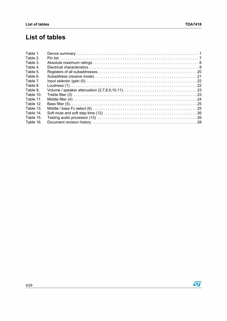
September 2013 Rev 4 1/29 1 TDA7418 3 band car audio processor Features • Input multiplexer – PD/SE4: pseudo differential stereo input, programmable as single-ended input – SE1: stereo single-end input – SE2: stereo single-end input – SE3: stereo single-end input – Input gain adjust from 0 to 15dB with 1dB steps – Internal offset-cancellation (AutoZero) • Loudness – Second order frequency response – Programmable center frequency (400 Hz / 800 Hz / 2400 Hz) – 15dB with 1dB steps – Selectable low and high frequency boost – Selectable flat-mode (constant attenuation) • Volume – +15dB to -79dB with 1dB step resolution – Soft-step control with programmable blend times • Bass – Second order frequency response – Center frequency programmable in 4 steps (60 Hz / 80 Hz / 100 Hz / 200 Hz) – Q programmable 1.0/1.25/1.5/2.0 – DC gain programmable – -15 to 15dB range with 1dB resolution • Middle – Second order frequency response – Center frequency programmable in 4 steps (500 Hz / 1 kHz / 1.5 kHz / 2.5 kHz) – Q programmable 0.5/0.75/1.0/1.25 – -15 to 15dB range with 1dB resolution • Treble – Second order frequency response – Center frequency programmable in 4 steps (10 kHz / 12.5 kHz / 15 kHz / 17.5 kHz) – -15 to 15dB range with 1dB resolution • Speaker – 4 independent soft step speaker controls, +15dB to -79dB with 1dB steps direct mute • Subwoofer – Single-ended mono output – Independent soft step level control, +15dB to -79dB with 1dB steps • Mute functions – Direct mute – Digitally controlled SoftMute with 3 programmable mute-times (0.48 ms / 0.96 ms /123 ms) Description The TDA7418 includes a high performance audio processor with fully integrated 3-Band filters to process signals at audible frequencies. The digital control allows a full programming of the audioprocessor and filters characteristics. SO20 Table 1. Device summary Order code Temp range, C Package Packing TDA7418 -40 to +85 SO20 Tube TDA7418TR -40 to +85 SO20 Tape and reel www.st.com
Transcript
September 2013 Rev 4 1/29
1
TDA7418
3 band car audio processor
Features
• Input multiplexer
– PD/SE4: pseudo differential stereo input, programmable as single-ended input
– Center frequency programmable in 4 steps (60 Hz / 80 Hz / 100 Hz / 200 Hz)
– Q programmable 1.0/1.25/1.5/2.0
– DC gain programmable
– -15 to 15dB range with 1dB resolution
• Middle
– Second order frequency response
– Center frequency programmable in 4 steps (500 Hz / 1 kHz / 1.5 kHz / 2.5 kHz)
– Q programmable 0.5/0.75/1.0/1.25
– -15 to 15dB range with 1dB resolution
• Treble
– Second order frequency response
– Center frequency programmable in 4 steps (10 kHz / 12.5 kHz / 15 kHz / 17.5 kHz)
– -15 to 15dB range with 1dB resolution
• Speaker
– 4 independent soft step speaker controls, +15dB to -79dB with 1dB steps direct mute
• Subwoofer
– Single-ended mono output
– Independent soft step level control, +15dB to -79dB with 1dB steps
• Mute functions
– Direct mute
– Digitally controlled SoftMute with 3 programmable mute-times(0.48 ms / 0.96 ms /123 ms)
Description
The TDA7418 includes a high performance audio processor with fully integrated 3-Band filters to process signals at audible frequencies. The digital control allows a full programming of the audioprocessor and filters characteristics.
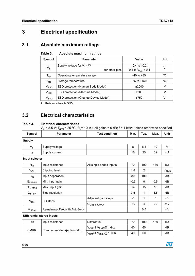
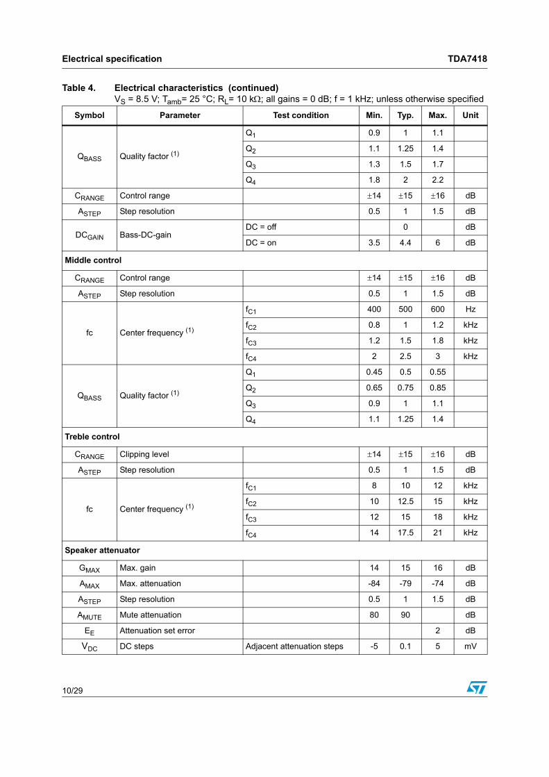
Symbol Parameter Test condition Min. Typ. Max. Unit
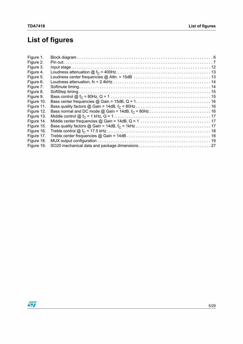
Description of the audioprocessor TDA7418
12/29
4 Description of the audioprocessor
4.1 Input stages
In the basic configuration, one stereo pseudo differential (programmable as single-ended input) and three single-ended stereo inputs are available.
Pseudo differential stereo input (PD/SE4)
The PD input is implemented as a buffered pseudo differential stereo stage with 100k input-impedance at each input. The attenuation is fixed to -3dB in order to adapt the incoming signal level. It is also configurable as single-ended input.
Single-ended stereo input (SE1, SE2, SE3)
The input-impedance at each input is 100k and the attenuation is fixed to -3dB for incoming signals.
Figure 3. Input stage
4.2 AutoZero
The AutoZero allows a reduction of the number of pins as well as external components by canceling any offset generated by or before the In-Gain-stage (Please notice that externally generated offsets, e.g. generated through the leakage current of the coupling capacitors, are not canceled).
The auto-zeroing is started every time the input source is changed and needs max. 0.6ms for the alignment. To avoid audible clicks the Audio processor is muted before the loudness stage during this time.
AutoZero-remain
In some cases, for example if the µP is executing a refresh cycle of the IIC-Bus-programming, it is not useful to start a new AutoZero-action because no new source is
QD/SE4QD_L/SE4_L
QD_R/SE4_R
QD_G
SE3
SE2SE2_L
SE2_R
QD/SE4
SE1
SE2
SE3
Input
Selector
In Gain
SE1SE1_L
SE1_R
SE3_L
SE3_R
TDA7418 Description of the audioprocessor
13/29
selected and an undesired mute would appear at the outputs. For such applications, it can be switched in the AutoZero-Remain-Mode (Bit 6 of the subaddress-byte). If this bit is set to high, the AutoZero will not be invoked and the old adjustment-value remains.
4.3 Loudness
There are four parameters programmable in the loudness stage:
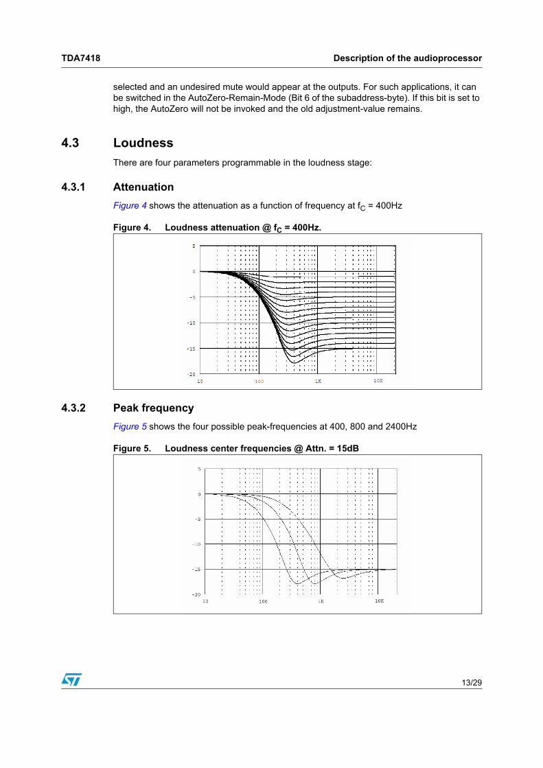
4.3.1 Attenuation
Figure 4 shows the attenuation as a function of frequency at fC = 400Hz
Figure 4. Loudness attenuation @ fC = 400Hz.
4.3.2 Peak frequency
Figure 5 shows the four possible peak-frequencies at 400, 800 and 2400Hz
Figure 5. Loudness center frequencies @ Attn. = 15dB
Description of the audioprocessor TDA7418
14/29
4.3.3 Low and high frequency boost
Figure 6 shows the different Loudness shapes in low & high frequency boost.
Figure 6. Loudness attenuation, fc = 2.4kHz
4.3.4 Flat mode
In flat mode the loudness stage works as a 0dB to -15dB attenuator.
4.4 SoftMute
The digitally controlled SoftMute stage allows muting/demuting the signal with a I2C-bus programmable slope. The mute process can either be activated by the SoftMute pin or by the I2C-bus. This slope is realized in a special S-shaped curve to mute slow in the critical regions (see Figure 7).
For timing purposes the Bit0 of the I2C-bus output register is set to 1 from the start of muting until the end of demuting.
Figure 7. Softmute timing
1. Please notice that a started Mute-action is always terminated and could not be interrupted by a change of the mute-signal
1EXT.
MUTE
+SIGNAL
REF
-SIGNAL
1
I2C BUSOUT
TimeD97AU634
TDA7418 Description of the audioprocessor
15/29
4.5 SoftStep volume
When the volume-level is changed audible clicks could appear at the output. The root cause of those clicks
could either be a DC-Offset before the volume-stage or the sudden change of the envelope of the audio signal. With the SoftStep-feature both kinds of clicks could be reduced to a minimum and are no more audible.
Eight programmable softstep time from one step to the next are user selectable.
Figure 8. SoftStep timing
1. For steps more than 1dB the SoftStep mode should be deactivated because it could generate 1dB error step during the blend-time.
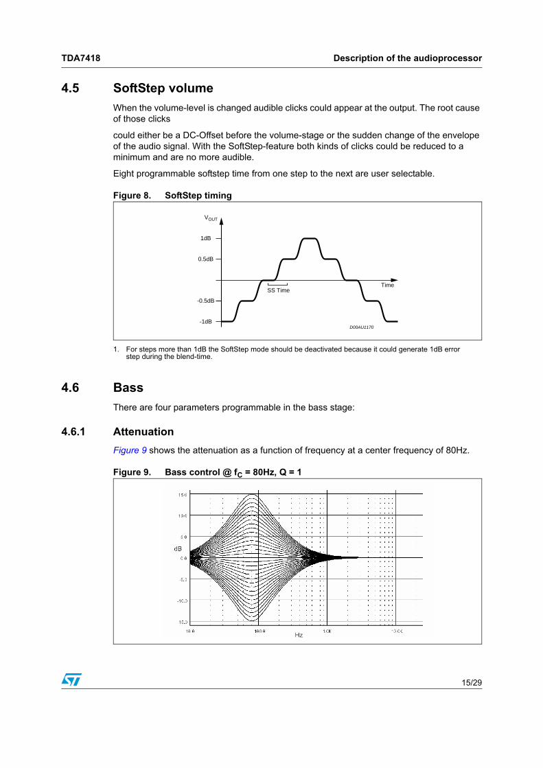
4.6 Bass
There are four parameters programmable in the bass stage:
4.6.1 Attenuation
Figure 9 shows the attenuation as a function of frequency at a center frequency of 80Hz.
Figure 9. Bass control @ fC = 80Hz, Q = 1
1dB
0.5dB
-0.5dB
-1dB
Time
D00AU1170
VOUT
SS Time
Description of the audioprocessor TDA7418
16/29
4.6.2 Center frequency
Figure 10 shows the four possible center frequencies 60, 80, 100 and 200Hz.
Figure 10. Bass center frequencies @ Gain = 15dB, Q = 1
4.6.3 Quality factors
Figure 11 shows the four possible quality factors 1, 1.25, 1.5 and 2.
Figure 11. Bass quality factors @ Gain = 14dB, fC = 80Hz
4.6.4 DC mode
In this mode the DC-gain is increased by 4.4dB. In addition the programmed center frequency and quality factor is decreased by 25% which can be used to reach alternative center frequencies or quality factors.
Figure 12. Bass normal and DC mode @ Gain = 14dB, fC = 80Hz
1. The center frequency, Q and DC-mode can be set fully independently.
TDA7418 Description of the audioprocessor
17/29
4.7 Middle
There are three parameters programmable in the middle stage:
4.7.1 Attenuation
Figure 13 shows the attenuation as a function of frequency at a center frequency of 1kHz.
Figure 13. Middle control @ fC = 1 kHz, Q = 1
4.7.2 Center frequency
Figure 14 shows the four possible center frequencies 500Hz, 1kHz, 1.5kHz and 2.5kHz.
Figure 14. Middle center frequencies @ Gain = 14dB, Q = 1
4.7.3 Quality factors
Figure 15 shows the four possible quality factors 0.5, 0.75, 1 and 1.5.
Figure 15. Bass quality factors @ Gain = 14dB, fC = 1kHz
Description of the audioprocessor TDA7418
18/29
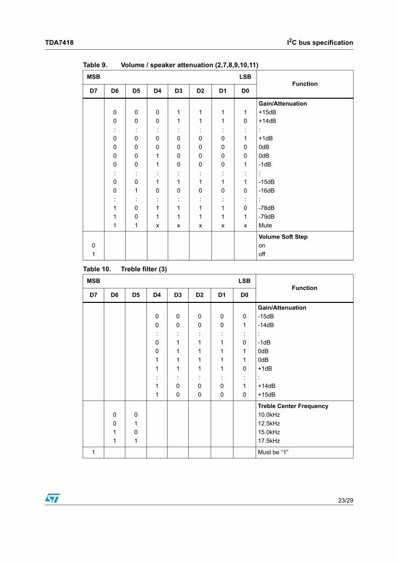
4.8 Treble
There are two parameters programmable in the treble stage:
4.8.1 Attenuation
Figure 16 shows the attenuation as a function of frequency at a center frequency of 17.5kHz.
Figure 16. Treble control @ fC = 17.5 kHz
4.8.2 Center frequency
Figure 17 shows the four possible center frequencies 10k, 12.5k, 15k and 17.5kHz.
Figure 17. Treble center frequencies @ Gain = 14dB
4.9 Speaker attenuator
The four speakers have independent soft step speaker controls. And their attenuators can be adjusted from +15dB to -79dB with 1dB steps.
4.10 Subwoofer attenuator
The Subwoofer output is a single ended mono output. The attenuator is exactly the same like the other speakers.
TDA7418 Description of the audioprocessor
19/29
4.11 MUX output
It provides a mono signal output (before tone filters) at Mute/MUX pin, used for external level meter / spectrum analyzer.
The mute pin can be configured as MUX output (I2C Byte13_D7D1). When it is configured as MUX output, the output voltage is (InGainL+InGainR)/2 with -3dB attenuation.
Figure 18. MUX output configuration
4.12 Audioprocessor testing
In the test mode, which can be activated by setting bit D7 of the IIC subaddress byte and bit D0 of the testing audioprocessor byte, several internal signals are available at the SE2R pin. In this mode, the input resistance of 100kOhm is disconnected from the pin. Internal signals available for testing are listed in the data-byte specification.
+
InGainL
InGainR
MUTE/MUX = (InGainL+InGainR)/2 * (-3dB)
AC00059
I2C bus specification TDA7418
20/29
5 I2C bus specification
5.1 Interface protocol
The interface protocol comprises:
– a start condition (S)
– a chip address byte (the LSB determines read/write transmission)
– a subaddress byte
– a sequence of data (N-bytes + acknowledge)
– a stop condition (P)
– the max. clock speed is 500kbits/s
5.1.1 Receive mode
S = Start
R/W = "0" -> Receive Mode (Chip can be programmed by P)
"1" -> Transmission Mode (Data could be received by P)
ACK = Acknowledge
P = Stop
TS = Testing mode
AZ = Auto zero remain
AI = Auto increment
5.1.2 Transmission mode
SM = Soft mute activated for main channel
X = Not Used
The transmitted data is automatic updated after each ACK. Transmission can be repeated without new chip address.
5.1.3 Reset condition
A Power-On-Reset is invoked if the Supply-Voltage is below than 2.5V. After that the following data is written automatically into the registers of all subaddresses:
S 1 0 0 0 1 0 0 R/W ACK TS AZ AI A4 A3 A2 A1 A0 ACK DATA ACK P
In order to meet environmental requirements, ST (also) offers these devices in ECOPACK® packages. ECOPACK® packages are lead-free. The category of second Level Interconnect is marked on the package and on the inner box label, in compliance with JEDEC Standard JESD97. The maximum ratings related to soldering conditions are also marked on the inner box label.
ECOPACK is an ST trademark. ECOPACK specifications are available at: www.st.com.
Figure 19. SO20 mechanical data and package dimensions
OUTLINE ANDMECHANICAL DATA
DIM.mm inch
MIN. TYP. MAX. MIN. TYP. MAX.
A 2.35 2.65 0.093 0.104
A1 0.10 0.30 0.004 0.012
B 0.33 0.51 0.013 0.200
C 0.23 0.32 0.009 0.013
D (1) 12.60 13.00 0.496 0.512
E 7.40 7.60 0.291 0.299
e 1.27 0.050
H 10.0 10.65 0.394 0.419
h 0.25 0.75 0.010 0.030
L 0.40 1.27 0.016 0.050
k 0˚ (min.), 8˚ (max.)
ddd 0.10 0.004
(1) “D” dimension does not include mold flash, protusions or gateburrs. Mold flash, protusions or gate burrs shall not exceed0.15mm per side.
Information in this document is provided solely in connection with ST products. STMicroelectronics NV and its subsidiaries (“ST”) reserve theright to make changes, corrections, modifications or improvements, to this document, and the products and services described herein at anytime, without notice.
All ST products are sold pursuant to ST’s terms and conditions of sale.
Purchasers are solely responsible for the choice, selection and use of the ST products and services described herein, and ST assumes noliability whatsoever relating to the choice, selection or use of the ST products and services described herein.
No license, express or implied, by estoppel or otherwise, to any intellectual property rights is granted under this document. If any part of thisdocument refers to any third party products or services it shall not be deemed a license grant by ST for the use of such third party productsor services, or any intellectual property contained therein or considered as a warranty covering the use in any manner whatsoever of suchthird party products or services or any intellectual property contained therein.
UNLESS OTHERWISE SET FORTH IN ST’S TERMS AND CONDITIONS OF SALE ST DISCLAIMS ANY EXPRESS OR IMPLIEDWARRANTY WITH RESPECT TO THE USE AND/OR SALE OF ST PRODUCTS INCLUDING WITHOUT LIMITATION IMPLIEDWARRANTIES OF MERCHANTABILITY, FITNESS FOR A PARTICULAR PURPOSE (AND THEIR EQUIVALENTS UNDER THE LAWSOF ANY JURISDICTION), OR INFRINGEMENT OF ANY PATENT, COPYRIGHT OR OTHER INTELLECTUAL PROPERTY RIGHT.
ST PRODUCTS ARE NOT DESIGNED OR AUTHORIZED FOR USE IN: (A) SAFETY CRITICAL APPLICATIONS SUCH AS LIFESUPPORTING, ACTIVE IMPLANTED DEVICES OR SYSTEMS WITH PRODUCT FUNCTIONAL SAFETY REQUIREMENTS; (B)AERONAUTIC APPLICATIONS; (C) AUTOMOTIVE APPLICATIONS OR ENVIRONMENTS, AND/OR (D) AEROSPACE APPLICATIONSOR ENVIRONMENTS. WHERE ST PRODUCTS ARE NOT DESIGNED FOR SUCH USE, THE PURCHASER SHALL USE PRODUCTS ATPURCHASER’S SOLE RISK, EVEN IF ST HAS BEEN INFORMED IN WRITING OF SUCH USAGE, UNLESS A PRODUCT ISEXPRESSLY DESIGNATED BY ST AS BEING INTENDED FOR “AUTOMOTIVE, AUTOMOTIVE SAFETY OR MEDICAL” INDUSTRYDOMAINS ACCORDING TO ST PRODUCT DESIGN SPECIFICATIONS. PRODUCTS FORMALLY ESCC, QML OR JAN QUALIFIED AREDEEMED SUITABLE FOR USE IN AEROSPACE BY THE CORRESPONDING GOVERNMENTAL AGENCY.
Resale of ST products with provisions different from the statements and/or technical features set forth in this document shall immediately voidany warranty granted by ST for the ST product or service described herein and shall not create or extend in any manner whatsoever, anyliability of ST.
ST and the ST logo are trademarks or registered trademarks of ST in various countries.Information in this document supersedes and replaces all information previously supplied.
The ST logo is a registered trademark of STMicroelectronics. All other names are the property of their respective owners.
Australia - Belgium - Brazil - Canada - China - Czech Republic - Finland - France - Germany - Hong Kong - India - Israel - Italy - Japan - Malaysia - Malta - Morocco - Philippines - Singapore - Spain - Sweden - Switzerland - United Kingdom - United States of America