3-Channel HDTV Video Amplifier With 5th-Order Filters and 6-dB Gain
• 3 HDTV Video Amplifiers for Y'P'BP'R 720p and1080i, G'B'R' (R'G'B'), VGA/SVGA/XGA Fabricated using the Silicon-Germanium (SiGe)
BiCom-III process, the THS7316 is a low power• Integrated Low-Pass Filterssingle-supply 3-V to 5-V, 3-channel integrated video– 5th-Order 36-MHz (–3 dB) Butterworth Filterbuffer. It incorporates a 5th-order modified
– –1 dB Passband Bandwidth at 31 MHz Butterworth filter which is useful as a DAC– 30 dB Attenuation at 74 MHz reconstruction filter or an ADC anti-aliasing filter. The
36-MHz filter is a perfect choice for HDTV video• Versatile Input Biasingwhich includes Y'P'BP'R 720p/1080i, G'B'R' (R'G'B'),– DC-Coupled With 140-mV Input Shift and VGA/SVGA/XGA signals.
– AC-Coupled with Sync-Tip ClampAs part of the THS7316 flexibility, the input can be
– Allows AC-Coupled With Biasing configured for ac or dc coupled inputs. The DC +• Built-in 6-dB Gain (2V/V) 140-mV input offset shift to allow for a full sync
dynamic range at the output with 0-V input. The AC• 3-V to 5-V Single Supply Operationcoupled modes include a transparent sync-tip clamp
• Rail-to-Rail Output: option for signals with sync such as Y’ or Green with– Output Swings Within 100 mV From the sync. AC-coupled biasing for P’B/P’R/Non-sync
channels can be achieved by adding an externalRails Allowing AC or DC Output Couplingresistor.– Supports Driving 2 Lines per ChannelThe THS7316 is the perfect choice for all output• Low 18.3-mA at 3.3-V Total Quiescent Currentbuffer applications. Its rail-to-rail output stage with• Low Differential Gain/Phase of 0.1% / 0.1° 6-dB gain allows for both ac and dc line driving. The
• SOIC-8 Package ability to drive 2 video lines per channel, or 75-Ωloads, allows for maximum flexibility as a video linedriver. The 18.3-mA total quiescent current makes itan excellent choice for USB powered, portable, or• Set Top Box Output Video Bufferingother power sensitive video applications.• PVR/DVDR Output Buffering
• USB/Portable Low Power Video Buffering The THS7316 is available in a small SOIC-8 packagethat is RoHS compliant.
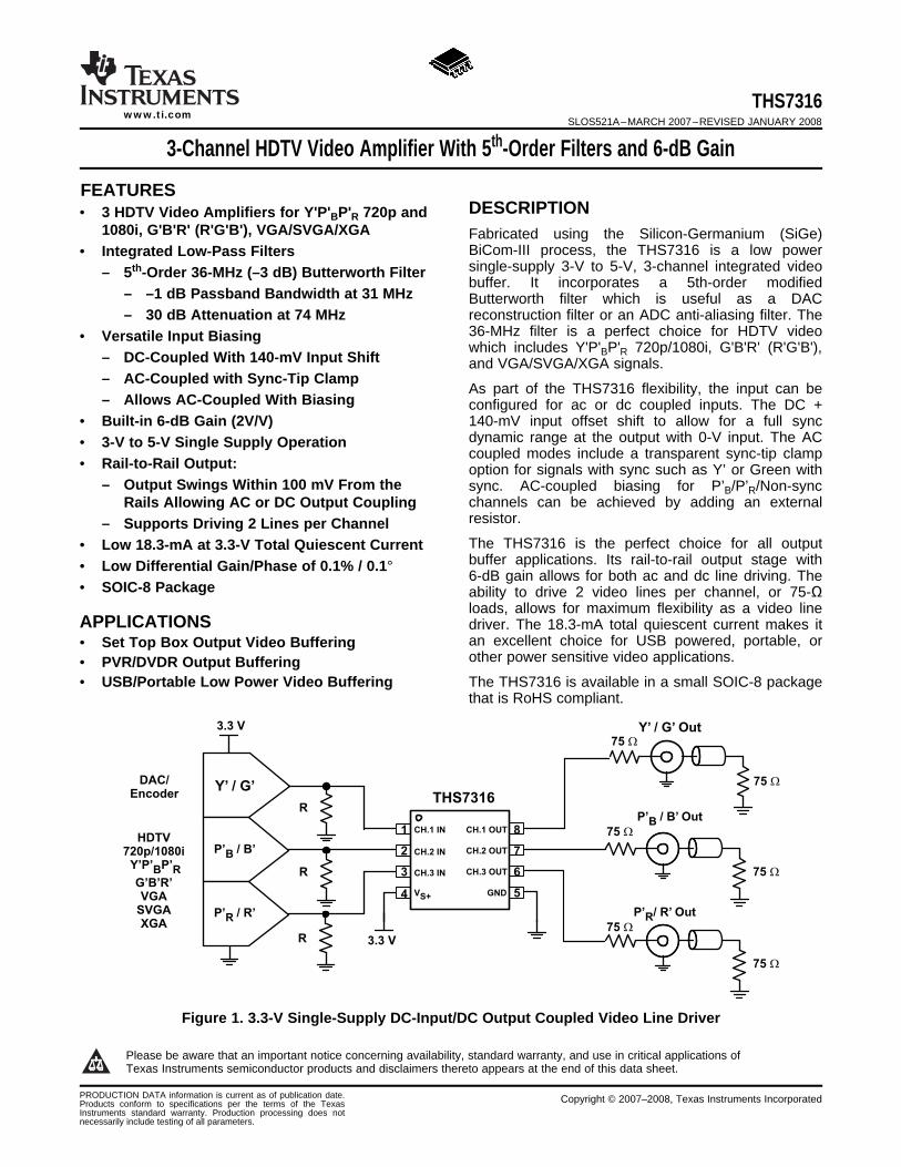
Figure 1. 3.3-V Single-Supply DC-Input/DC Output Coupled Video Line Driver1
Please be aware that an important notice concerning availability, standard warranty, and use in critical applications ofTexas Instruments semiconductor products and disclaimers thereto appears at the end of this data sheet.
This integrated circuit can be damaged by ESD. Texas Instruments recommends that all integrated circuits be handled withappropriate precautions. Failure to observe proper handling and installation procedures can cause damage.
ESD damage can range from subtle performance degradation to complete device failure. Precision integrated circuits may be moresusceptible to damage because very small parametric changes could cause the device not to meet its published specifications.
PACKAGING/ORDERING INFORMATIONPACKAGED DEVICES PACKAGE TYPE (1) TRANSPORT MEDIA, QUANTITY
THS7316D Rails, 75SOIC-8
THS7316DR Tape and Reel, 2500
(1) For the most current package and ordering information, see the Package Option Addendum at the end of this document, or see the TIWeb site at www.ti.com.
over operating free-air temperature range (unless otherwise noted) (1)
VALUE UNITSupply voltage, VS+ to GND 5.5 V
VI Input voltage –0.4 V to VS+ VIO Output current ±90 mA
Continuous power dissipation See Dissipation Rating TableTJ Maximum junction temperature, any condition (2) 150 °CTJ Maximum junction temperature, continuous operation, long term reliability (3) 125 °CTstg Storage temperature range –65 to 150 °C
HBM 2000ESD ratings CDM 1500 V
MM 200
(1) Stresses above those listed under absolute maximum ratings may cause permanent damage to the device. These are stress ratingsonly and functional operation of the device at these or any other conditions beyond those indicated under recommended operatingconditions is not implied. Exposure to absolute maximum rated conditions for extended periods may degrade device reliability.
(2) The absolute maximum junction temperature under any condition is limited by the constraints of the silicon process.(3) The absolute maximum junction temperature for continuous operation is limited by the package constraints. Operation above this
temperature may result in reduced reliability and/or lifetime of the device.
POWER RATING (1)θJC θJA (TJ = 125°C)PACKAGE (°C/W) (°C/W)
TA = 25°C TA = 85°CSOIC-8 (D) 16.8 130 (2) 769 mW 308 mW
(1) Power rating is determined with a junction temperature of 125°C. This is the point where performance starts to degrade and long-termreliability starts to be reduced. Thermal management of the final PCB should strive to keep the junction temperature at or below 125°Cfor best performance and reliability.
(2) This data was taken with the JEDEC High-K test PCB. For the JEDEC low-K test PCB, the θJA is 196°C/W.
MIN MAX UNITVS+ Supply voltage 3 5 VTA Ambient temperature –40 85 °C
CH. 1 – INPUT 1 I Video Input – Channel 1CH. 2 – INPUT 2 I Video Input – Channel 2CH. 3 – INPUT 3 I Video Input – Channel 3+Vs 4 I Positive Power Supply Pin – connect to 3 V to 5 V.GND 5 I Ground Pin for all internal circuitry.CH. 3 – OUTPUT 6 O Video Output – Channel 3CH. 2 – OUTPUT 7 O Video Output – Channel 2CH. 1 – OUTPUT 8 O Video Output – Channel 1
Attenuation f = 27 MHz (2) 0.3 –0.3/2.4 –0.35/2.4 –0.4/2.6 dB Min/Max
With respect to 100 kHz f = 74 MHz (2) 30 20 19 19 dB Min
Group delay f = 100 kHz 16.2 ns Typ
Group delay variation f = 27 MHz 5.4 ns Typwith respect to 100 kHz
Channel-to-channel delay 0.3 ns Typ
Differential gain NTSC / PAL 0.1 / Typ0.15%
Differential phase NTSC / PAL 0.1 / 0.1 ° Typ
Total harmonic distortion f = 1 MHz; VO = 2 VPP –70 dB Typ
Signal to noise ratio No Weighting, 100 kHz to 37.5 MHz 67 dB Typ
Channel-to-channel crosstalk f = 1 MHz –61 dB Typ
AC Gain – All channels 6 5.7/6.3 5.65/6.35 5.65/6.35 dB Min/Max
Output Impedance f = 10 MHz 0.5 Ω Typ
DC PERFORMANCE
Biased output voltage VI = 0 V 285 210/370 200/380 190/390 mV Min/Max
Input voltage range DC input, limited by output –0.1/1.46 V Typ
Sync tip clamp charge current VI = –0.1 V 360 µA Typ
Input resistance 800 kΩ Typ
Input capacitance 2 pF Typ
OUTPUT CHARACTERISTICS
RL = 150 Ω to 1.65V 3.15 V Typ
RL = 150 Ω to GND 3.1 2.85 2.75 2.75 V MinHigh output voltage swing
RL = 75 Ω to 1.65V 3.1 V Typ
RL = 75 Ω to GND 3.0 V Typ
RL = 150 Ω to 1.65V (VI = –0.15 V) 0.14 V Typ
RL = 150 Ω to GND (VI = –0.15 V) 0.08 0.17 0.2 0.21 V MaxLow output voltage swing
RL = 75 Ω to 1.65V (VI = –0.15 V) 0.3 V Typ
RL = 75 Ω to GND (VI = –0.15 V) 0.1 V Typ
Output current (sourcing) RL = 10 Ω to 1.65V 80 mA Typ
Output current (sinking) RL = 10 Ω to 1.65V 70 mA Typ
POWER SUPPLY
Maximum operating voltage 3.3 5.5 5.5 5.5 V Max
Minimum operating voltage 3.3 2.85 2.85 2.85 V Min
Maximum quiescent current VI = 0 V 18.3 22.5 23 23.4 mA Max
Minimum quiescent current VI = 0 V 18.3 14 13.6 13.1 mA Min
Power Supply Rejection (+PSRR) 52 dB Typ
(1) The Min/Max values listed for this specification are specified by design and characterization only.(2) 3.3-V Supply Filter specifications are specified by 100% testing at 5-V supply along with design and characterization only.
The THS7316 is targeted for standard definition video output buffer applications. Although it can be used fornumerous other applications, the needs and requirements of the video signal is an important design parameter ofthe THS7316. Built on the Silicon Germanium (SiGe) BiCom-3 process, the THS7316 incorporates manyfeatures not typically found in integrated video parts while consuming low power.
The THS7316 has the following features:• Single-Supply 3-V to 5-V operation with low total quiescent current of 18.3-mA at 3.3-V and 19.3-mA at 5-V.• Input configuration accepting DC + Level shift, AC Sync-Tip Clamp.• AC-Biasing is accomplished with the use of an external pull-up resistor to the positive power supply.• 5th-Order Low Pass Filter for DAC reconstruction or ADC image rejection:
– 36-MHz for HDTV, Y'P'BP'R 720p/1080i, G'B'R' (R'G'B'), and Computer VGA/SVGA/XGA signals.– Can also be used for SDTV (480i, 576i, CVBS, S-Video), and EDTV (480p and 576p) signals if desired.
• Internal fixed gain of 2 V/V (6 dB) buffer that can drive up to 2 video lines per channel with dc coupling ortraditional ac coupling.
• Signal flow-through configuration using an 8-pin SOIC package that complies with the latest (RoHScompatible) and Green manufacturing requirements.
The THS7316 is designed to operate from 3-V to 5-V over a –40°C to 85°C temperature range. The impact onperformance over the entire temperature range is negligible due to the implementation of thin film resistors andhigh quality – low temperature coefficient capacitors.
The power supply pins should have a 0.1-µF to 0.01-µF capacitor placed as close as possible to these pins.Failure to do so may result in the THS7316 outputs ringing or have an oscillation. Additionally, a large capacitor,such as 22 µF to 100 µF, should be placed on the power supply line to minimize interference with 50/60 Hz linefrequencies.
The THS7316 input range allows for an input signal range from –0.3 V to about (Vs+ – 1.5 V). But, due to theinternal fixed gain of 2 V/V (6 dB) and the internal level shift of nominally 140-mV, the output is generally thelimiting factor for the allowable linear input range. For example, with a 5-V supply, the linear input range is from–0.3 V to 3.5 V. However, due to the gain and level shift, the linear output range limits the allowable linear inputrange to be from about –0.1 V to 2.3 V.
The THS7316 is built using a high-speed complementary bipolar and CMOS process. The internal junctionbreakdown voltages are low for these small geometry devices. These breakdowns are reflected in the AbsoluteMaximum Ratings table. All input and output device pins are protected with internal ESD protection diodes to thepower supplies, as shown in Figure 26.
These diodes provide moderate protection to input overdrive voltages above and below the supplies as well. Theprotection diodes can typically support 30-mA of continuous current when overdriven.
A typical application circuit using the THS7316 as a video buffer is shown in Figure 27. It shows a DAC (orencoder such as the THS8200) driving the three input channels of the THS7316. Although these channels showHDTV Y'P'BP'R (sometimes labeled Y'C'BC'R) signals of a 720p or 1080i system, they can also be G'B'R' (R'G'B')signals or other variations.
Note that the Y' term is used for the luma channels throughout this document rather than the more commonluminance (Y) term. The reason is to account for the definition of luminance as stipulated by the CIE –International Commission on Illumination. Video departs from true luminance since a nonlinear term, gamma, isadded to the true RGB signals to form R'G'B' signals. These R'G'B' signals are then used to mathematicallycreate luma (Y'). Thus luminance (Y) is not maintained providing a difference in terminology.
This rationale is also used for the chroma (C') term. Chroma is derived from the non-linear R'G'B' terms and thusit is nonlinear. Chrominance (C) is derived from linear RGB giving the difference between chroma (C') andchrominance (C). The color difference signals (P'B / P'R / U' / V') are also referenced this way to denote thenonlinear (gamma corrected) signals.
R'G'B' (commonly mislabeled RGB) is also called G’B’R’ (again commonly mislabeled as GBR) in professionalvideo systems. The SMPTE component standard stipulates that the luma information is placed on the firstchannel, the blue color difference is placed on the second channel, and the red color difference signal is placedon the third channel. This is consistent with the Y'P'BP'R nomenclature. Because the luma channel (Y') carries thesync information and the green channel (G') also carries the sync information, it makes logical sense that G' beplaced first in the system. Since the blue color difference channel (P'B) is next and the red color differencechannel (P'R) is last, then it also makes logical sense to place the B' signal on the second channel and the R'signal on the third channel, respectively . Thus hardware compatibility is better achieved when using G'B'R'rather than R'G'B'. Note that for many G'B'R' systems sync is embedded on all three channels, but may notalways be the case in all systems.
Figure 27. Typical HDTV Y'/P'B/P'R Inputs From DC-Coupled Encoder/DACWith AC-Coupled Line Driving
The inputs to the THS7316 allows for both ac-coupled and dc-coupled inputs. Many DACs or Video Encoderscan be dc connected to the THS7316. One of the drawbacks to dc coupling is when 0-V is applied to the input.Although the input of the THS7316 allows for a 0-V input signal with no issues, the output swing of a traditionalamplifier cannot yield a 0-V signal resulting in possible clipping. This is true for any single-supply amplifier due tothe limitations of the output transistors. Both CMOS and bipolar transistors cannot go to 0-V while sinkingcurrent. This trait of a transistor is also the same reason why the highest output voltage is always less than thepower supply voltage when sourcing current.
This output clipping can reduce the sync amplitudes (both horizontal and vertical sync amplitudes) on the videosignal. A problem occurs if the receiver of this video signal uses an AGC loop to account for losses in thetransmission line. Some video AGC circuits derive gain from the horizontal sync amplitude. If clipping occurs onthe sync amplitude, then the AGC circuit can increase the gain too much – resulting in too much amplitude gaincorrection. This may result in a picture with an overly bright display with too much color saturation.
It is good engineering design practice to ensure saturation/clipping does not take place. Transistors always takea finite amount of time to come out of saturation. This saturation could possibly result in timing delays or otheraberrations on the signals.
To eliminate saturation/clipping problems, the THS7316 has a dc + 140-mV input shift feature. This feature takesthe input voltage and adds an internal +140-mV shift to the signal. Since the THS7316 also has a gain of 6 dB (2V/V), the resulting output with a 0-V applied input signal is about 280-mV. The THS7316 rail-to-rail output stagecan create this output level while connected to a typical video load. This ensures that no saturation / clipping ofthe sync signals occur. This is a constant shift regardless of the input signal. For example, if a 1-V input isapplied, the output is at 2.28-V.
Because the internal gain is fixed at 6 dB, the gain dictates what the allowable linear input voltage range can bewithout clipping concerns. For example, if the power supply is set to 3-V, the maximum output is about 2.9-Vwhile driving a significant amount of current. Thus, to avoid clipping, the allowable input is ((2.9 V / 2) – 0.14 V) =1.31 V. This is true for up to the maximum recommended 5-V power supply that allows about a ((4.9V / 2) – 0.14V) = 2.31 V input range while avoiding clipping on the output.
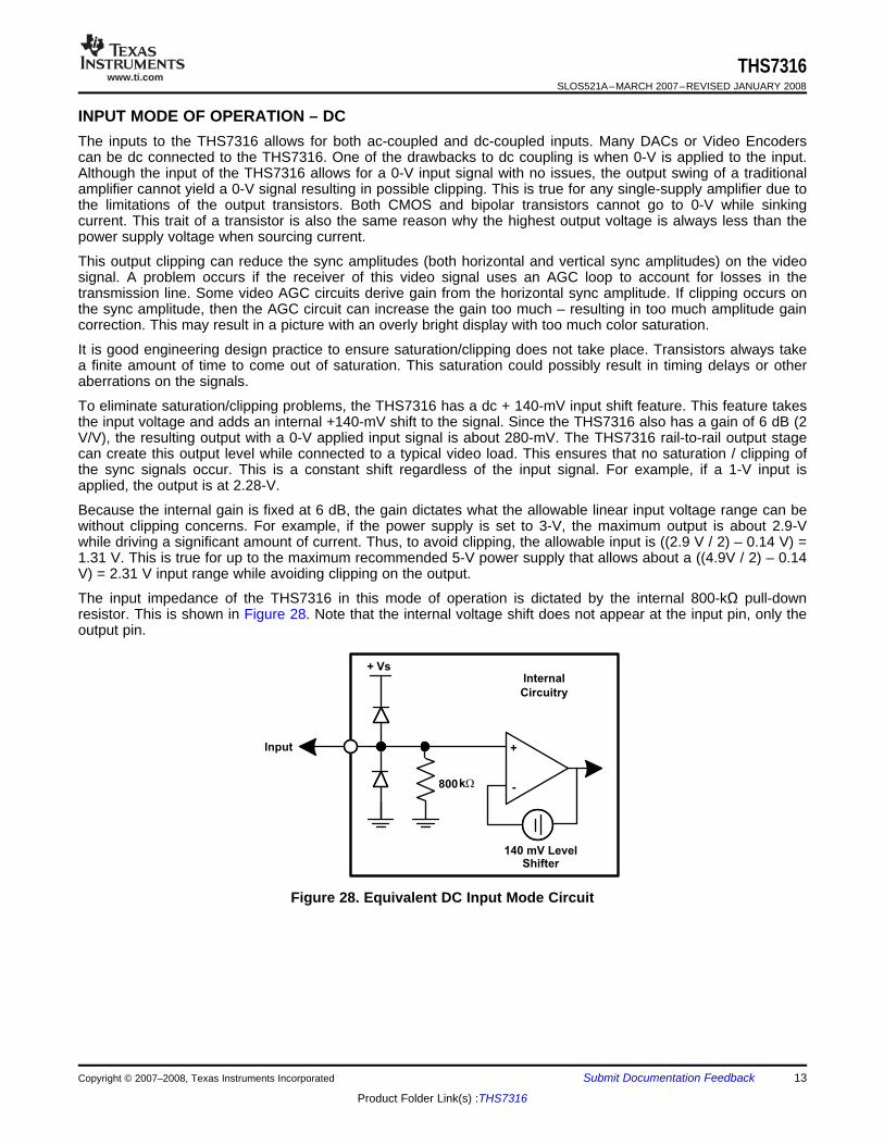
The input impedance of the THS7316 in this mode of operation is dictated by the internal 800-kΩ pull-downresistor. This is shown in Figure 28. Note that the internal voltage shift does not appear at the input pin, only theoutput pin.
Some video DACs or encoders are not referenced to ground but rather to the positive power supply. TheseDACs typically only sink current rather than the more traditional current sourcing DAC where the resistor isreferenced to ground. The resulting video signals can be too high of a voltage for a dc-coupled video buffer tofunction properly. To account for this scenario the THS7316 incorporates a sync-tip clamp circuit. This functionrequires a capacitor (nominally 0.1 µF) to be in series with the input. Note, while the term sync-tip-clamp is usedthroughout this document, it should be noted that the THS7316 is better termed as a dc-restoration circuit basedon how this function is performed. This circuit is an active clamp circuit and not a passive diode clamp function.
The input to the THS7316 has an internal control loop which sets the lowest input applied voltage to clamp atground (0-V). By setting the reference at 0-V, the THS7316 allows a dc-coupled input to also function. Hence,the STC is considered transparent since it does not operate unless the input signal goes below ground. Thesignal then goes through the same 140-mV level shifter resulting in an output voltage low level of 280-mV. If theinput signal tries to go below the 0-V, the internal control loop of the THS7316 will source up to 3-mA of currentto increase the input voltage level on the THS7316 input side of the coupling capacitor. As soon as the voltagegoes above the 0-V level, the loop stops sourcing current and becomes high impedance.
One of the concerns about the sync-tip-clamp level is how the clamp reacts to a sync edge that hasovershoot—common in VCR signals or reflections found in poor PCB layouts. Ideally the STC should not react tothe overshoot voltage of the input signal. Otherwise, this could result in clipping on the rest of the video signal asit may raise the bias voltage too much.
To help minimize this input signal overshoot problem, the control loop in the THS7316 has an internal low-passfilter as shown in Figure 29. This filter reduces the response time of the STC circuit. This delay is a function ofhow far the voltage is below ground, but in general it is about a 80-ns delay. The effect of this filter is to slowdown the response of the control loop so as not to clamp on the input overshoot voltage, but rather the flatportion of the sync signal.
As a result of this delay, the sync may have an apparent voltage shift. The amount of shift is dependant upon theamount of droop in the signal as dictated by the input capacitor and the STC current flow. Because the sync isprimarily for timing purposes with syncing occurring on the edge of the sync signal, this shift is transparent inmost systems.
While this feature may not fully eliminate overshoot issues on the input signal for excessive overshoot and/orringing, the STC system should help minimize improper clamping levels. As an additional method to helpminimize this issue, an external capacitor (ex: 10 pF to 47 pF) to ground in parallel with the external terminationresistors can help filter overshoot problems.
It should be noted that this STC system is dynamic and does not rely upon timing in any way. It only depends onthe voltage appearing at the input pin at any given point in time. The STC filtering helps minimize level shiftproblems associated with switching noises or very short spikes on the signal line. This helps ensure a veryrobust STC system.
Figure 29. Equivalent AC Sync Tip Clamp Input Circuit
When the AC Sync-Tip-Clamp (STC) operation is used, there must also be some finite amount of discharge bias
current. As previously described, if the input signal goes below the 0-V clamp level, the internal loop of theTHS7316 will source current to increase the voltage appearing at the input pin. As the difference between thesignal level and the 0-V reference level increases, the amount of source current increasesproportionally—supplying up to 3-mA of current. Thus the time to re-establish the proper STC voltage can befast. If the difference is small, then the source current is also small to account for minor voltage droop.
But, what happens if the input signal goes above the 0-V input level? The problem is the video signal is alwaysabove this level, and must not be altered in any way. But if the Sync level of the input signal is above this 0-Vlevel, then the internal discharge (sink) current will discharge the ac-coupled bias signal to the proper 0-V level.
This discharge current must not be large enough to alter the video signal appreciably, or picture quality issuesmay arise. This is often seen by looking at the tilt (aka droop) of a constant luma signal being applied and lookingat the resulting output level. The associated change in luma level from the beginning of the video line to the endof the video line is the amount of line tilt (droop).
If the discharge current is small, the amount of tilt is low which is good. But, the amount of time for the system tocapture the sync signal could be too long. This is also termed hum rejection. Hum arises from the ac line voltagefrequency of 50-Hz or 60-Hz. The value of the discharge current and the ac-coupling capacitor combine to dictatethe hum rejection and the amount of line tilt.
To allow for both dc-coupling and ac-coupling in the same part, the THS7316 incorporates an 800-kΩ resistor toground. Although a true constant current sink is preferred over a resistor, there are significant issues when thevoltage is near ground. This can cause the current sink transistor to saturate and cause potential problems withthe signal. This resistor is large enough as to not impact a dc-coupled DAC termination. For discharging anac-coupled source, Ohm’s Law is used. If the video signal is 1 V, then there is 1 V / 800 kΩ = 1.25-µA ofdischarge current. If more hum rejection is desired or there is a loss of sync occurring, then decrease the 0.1-µFinput coupling capacitor. A decrease from 0.1 µF to 0.047 µF increases the hum rejection by a factor of 2.1.Alternatively an external pull-down resistor to ground may be added which decreases the overall resistance, andultimately increases the discharge current.
To ensure proper stability of the AC STC control loop, the source impedance must be less than 1-kΩ with theinput capacitor in place. Otherwise, there is a possibility of the control loop to ring and this ringing may appear onthe output of the THS7316. Because most DACs or encoders use resistors to establish the voltage, which aretypically less than 300-Ω, then meeting the <1-kΩ requirement is done. But, if the source impedance looking fromthe THS7316 input perspective is high, then add a 1-kΩ resistor to GND to ensure proper operation of theTHS7316.
Sync tip clamps work well for signals that have horizontal and/or vertical syncs associated with them. But, somevideo signals do not have a sync embedded within the signal – such as Chroma or the P’B and P’R channels of a480i/480p/576i/576p signal; or the bottom of the sync is not the lowest possible level of the video signal – suchas the P’B and P’R channels of a 720p and 1080i signal. If ac-coupling of these signals is desired, then a dc biasis required to properly set the dc operating point within the THS7316. This function is easily accomplished withthe THS7316 by adding an external pull-up resistor to the positive power supply as shown in Figure 30.
The dc voltage appearing at the input pin is approximately equal to:VDC = VS+ × (800k ÷ (800k + RPU))
The THS7316 allowable input range is approximately (VS+ – 1.5 V) which allows for a wide input voltage range.As such, the input dc-bias point is flexible with the output dc-bias point being the primary factor. For example, ifthe output dc-bias point is desired to be 1.65 V on a 3.3-V supply, then the input dc-bias point should be (1.65 V– 280 mV) /2 = 0.685 V. Thus, the pull-up resistor calculates to about 3.01-MΩ resulting in 0.693 V. If the inputdc-bias point is desired to be 0.685 V with a 5-V power supply, then the pull-up resistor calculates to about5.1 MΩ.
The internal 800-kΩ resistor has approximately a ±20% variance. As such, the calculations should take this intoaccount. For the 0.693 V example above using an ideal 3.01-MΩ resistor, the input dc-bias voltage is about0.693 V ±0.11 V.
One other issue that must be taken into account is that the dc-bias point is a function of the power supply. Assuch, there may be an impact on power supply rejection (PSRR) on the system. To help reduce the impact, theinput capacitor combined with the pull-up resistance functions as a low-pass filter. Additionally, the time to chargethe capacitor to the final dc-bias point is also a function of the pull-up resistor and the input capacitor. Lastly, theinput capacitor forms a high-pass filter with the parallel impedance of the pull-up resistor and the 800-kΩ resistor.It is good to have this high pass filter at about 3-Hz to minimize any potential droop on a P'B, P'R, or non-syncsignals. A 0.1-µF input capacitor with a 3.01-MΩ pull-up resistor equates to about a 2.5-Hz high-pass cornerfrequency.
This mode of operation is recommended for use with chroma (C'), P’B, P'R, U', V', and non-sync B' and/or R'signals.
The THS7316 incorporates a rail-to-rail output stage that can be used to drive the line directly without the needfor large ac-coupling capacitors as shown in Figure 31. This offers the best line tilt and field tilt (or droop)performance since there is no ac-coupling occurring. Remember that if the input is ac-coupled, then the resultingtilt due to the input ac-coupling is seen on the output regardless of the output coupling. The 80-mA output currentdrive capability of the THS7316 was designed to drive two video lines per channel simultaneously – essentially a75-Ω load – while keeping the output dynamic range as wide as possible.
Figure 31. Typical HDTV Y'P'BP'R / G'B'R' System with DC-Coupled Line Driving
One concern of dc-coupling is if the line is terminated to ground. If the ac-bias input configuration is used, theoutput of the THS7316 will have a dc-bias on the output. With 2 lines terminated to ground, this creates adc-current path to exist which results in a slightly decreased high output voltage swing and resulting in anincrease in power dissipation of the THS7316. While the THS7316 was designed to operate with a junctiontemperature of up to 125°C, care must be taken to ensure that the junction temperature does not exceed thislevel or else long term reliability could suffer. Although this configuration only adds less than 10 mW of powerdissipation per channel, the overall low power dissipation of the THS7316 design minimizes potential thermalissues even when using the SOIC package at high ambient temperatures.
Another concern of dc coupling is the blanking level voltage of the video signal. The EIA specification dictatesthat the blanking level shall be 0 V ±1 V. While there is some question as to whether this voltage is at the outputof the amplifier or at the receiver, it is generally regarded to be measured at the receiver side of a system as therest of the specification voltage requirements are given with doubly terminated connections present. With therail-to-rail output swing capability, combined with the 140-mV input level shift, meeting this requirement isaccomplished. Thus, elimination of the large output ac-coupling capacitor can be done while still meeting the EIAspecification. This can save significant PCB area and costs.
Note that the THS7316 can drive the line with dc-coupling regardless of the input mode of operation. The onlyrequirement is to make sure the video line has proper termination in series with the output – typically 75-Ω. Thishelps isolate capacitive loading effects from the THS7316 output. Failure to isolate capacitive loads may result ininstabilities with the output buffer potentially causing ringing or oscillations to appear. The stray capacitanceappearing directly at the THS7316 output pins should be kept below 20-pF.
The most common method of coupling the video signal to the line is with the use of a large capacitor. Thiscapacitor is typically between 220-µF and 1000-µF, although 330-µF is common. This value of this capacitormust be this large to minimize the line tilt (droop) and/or field tilt associated with ac-coupling as describedpreviously in this document. AC-coupling is done for several reasons, but the most common reason is to ensurefull inter-operability with the receiving video system. This ensures that regardless of the reference dc voltageused on the transmit side, the receive side will re-establish the dc reference voltage to its own requirements, andmeets EIA specifications.
Like the dc-output mode of operation, each line should have a 75-Ω source termination resistor in series with theac-coupling capacitor. If 2 lines are to be driven, it is best to have each line use its own capacitor and resistorrather than sharing these components as shown in Figure 32. This helps ensure line-to-line dc isolation and thepotential problems as stipulated previously. Using a single 1000-µF capacitor for 2-lines can be done, but there isa chance for interference to be created between the two receivers.
Due to the edge rates and frequencies of operation, it is recommended – but not required – to place a 0.1-µF to0.01-µF capacitor in parallel with the large 220-µF to 1000-µF capacitor. These large value capacitors are mostcommonly aluminum electrolytic. These capacitors have significantly large ESR (equivalent series resistance),and their impedance at high frequencies is large due to the associated inductances involved with the leads andconstruction. The small 0.1-µF to 0.01-µF capacitors help pass these high frequency (>1 MHz) signals with muchlower impedance than the large capacitors.
Although it is common to use the same capacitor values for all the video lines, the frequency bandwidth of thechroma signal in a S-Video system are not required to go as low – or as high of a frequency – as the lumachannels. Thus the capacitor values of the chroma line(s) can be smaller – such as 0.1-µF.
A. Due to the high frequency content of the video signal, it is recommended, but not required, to add a 0.1-µF or 0.01-µFcapacitor in parallel with these large capacitors.
B. Current sinking DAC / Encoder shown. See the application notes.
Figure 32. Typical 480i/576i Y'P'BP'R AC-Input System Driving 2 AC-Coupled Video Lines
Each channel of the THS7316 incorporates a 5th-Order Low Pass Filter. These video reconstruction filtersminimize DAC images from being passed onto the video receiver. Depending on the receiver design, failure toeliminate these DAC images can cause picture quality problems due to aliasing of the ADC. Another benefit ofthe filter is to smooth out aberrations in the signal which some DACs can have if their own internal filtering is notgood. This helps with picture quality and helps insure the signal meets video bandwidth requirements.
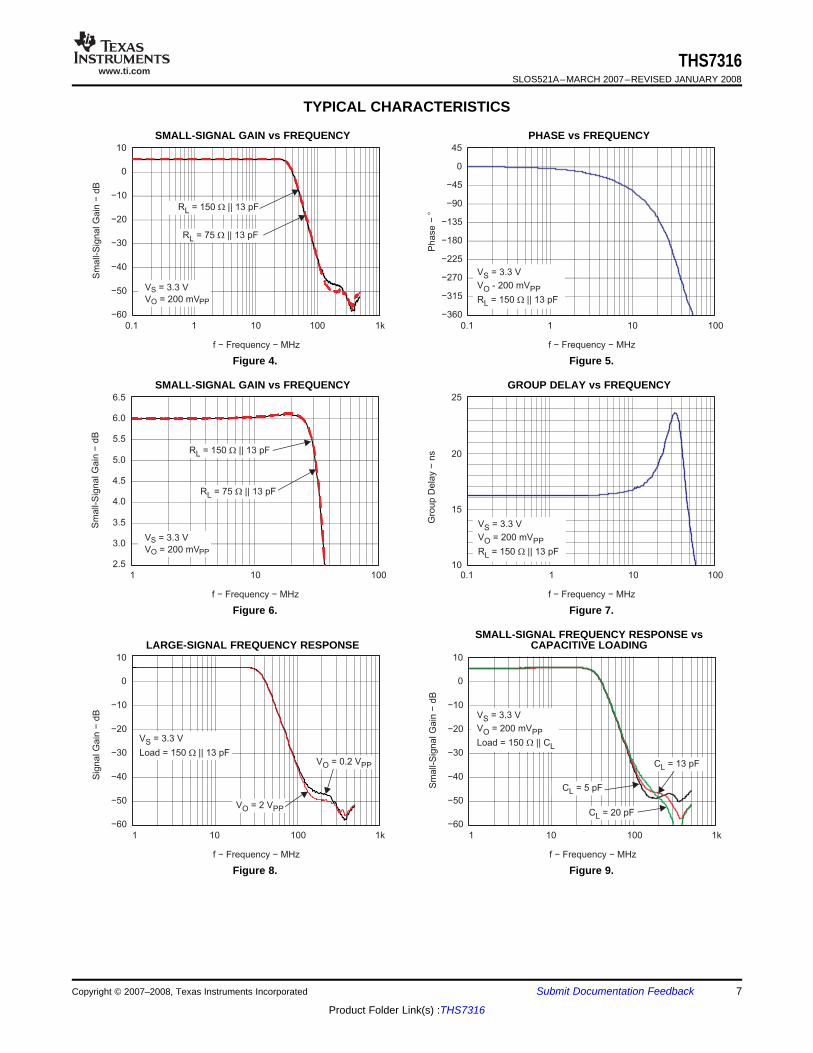
Each filter in the THS7316 is associated with a Butterworth characteristic. The benefit of the Butterworthresponse is that the frequency response is flat with a relatively steep initial attenuation at the corner frequency.The problem is that the group delay rises near the corner frequency. Group delay is defined as the change inphase (radians/second) divided by a change in frequency. An increase in group delay corresponds to a timedomain pulse response that has overshoot and some possible ringing associated with the overshoot.
The use of other type of filters, such as elliptic or chebyshev, are not recommended for video applications due totheir very large group delay variations near the corner frequency resulting in significant overshoot and ringing.While these elliptic or chebyshev filters may help meet the video standard specifications with respect toamplitude attenuation, their group delay is beyond the standard specifications. Coupled with the fact that videocan go from a white pixel to a black pixel over and over again, ringing can occur. Ringing typically causes adisplay to have ghosting or fuzziness appear on the edges of a sharp transition. However, a Bessel filter has anideal group delay response, but the rate of attenuation is typically too low for acceptable image rejection. Thusthe Butterworth filter is a respectable compromise for both attenuation and group delay.
The THS7316 filters have a nominal corner (-3dB) frequency at 36-MHz and a –1 dB passband typically at31-MHz. This 36-MHz filter is ideal for High Definition (HD) 720p and 1080i signals. For systems that oversamplesignificantly, the THS7316 can also be useful for Standard Definition (SD) NTSC and PAL signals such as480i/576i Y'P'BP'R, Y'U'V', and broadcast G’B’R’ (R’G’B’) signals. It can also be useful with Enhanced Definition(ED) signals including 480p/576p Y'P'BP'R, Y'U'V', broadcast G’B’R’ (R’G’B’) signals, and computer video signals.
The 36-MHz -3dB corner frequency was designed to allow a maximally flat video signal while achieving 30-dB ofattenuation at 74.25-MHz – a common sampling frequency between the DAC/ADC 2nd and 3rd Nyquist zonesfound in many video systems. This is important because any signal appearing around this frequency can appearin the baseband due to aliasing effects of an analog to digital converter found in a receiver. Keep in mind thatDAC images do not stop at 74.25 MHz, they continue around the sampling frequencies of 148.5 MHz,222.75-MHz, 297-MHz, etc. Because of these multiple images that an ADC can fold down into the basebandsignal, the low pass filter must also eliminate these higher order images. The THS7316 has over 50-dBattenuation at 148.5-MHz, over 50-dB attenuation at 222.75-MHz, and about 55-dB attenuation at 297-MHz.Attenuation to 1-GHz is at least 36-dB which makes sure that images do not effect the desired video basebandsignal.
The 36-MHz filter frequency was chosen to account for process variations in the THS7316. To ensure therequired video frequencies are not affected, the filter corner frequency must be high enough to allow componentvariations. The other consideration is the attenuation must be large enough to ensure the anti-aliasing /reconstruction filtering is enough to meet the system demands. Thus, the filter frequencies were not arbitrarilyselected.
Two key benefits of using an integrated filter system, such as the THS7316, over a passive system is PCB areaand filter variations. The small SOIC-8 package (3-video channels) is much smaller over a passive RLC network,especially a 5-pole passive network. Additionally, inductors have at best ±10% tolerances (normally ±15% to±20% is common) and capacitors typically have ±10% tolerances. Using a Monte Carlo analysis shows that thefilter corner frequency (–3 dB), flatness (–1 dB), Q factor (or peaking), and channel-to-channel delay has widevariations. This can lead to potential performance and quality issues in mass-production environments. TheTHS7316 solves most of these problems by using the corner frequency as essentially the only variable.
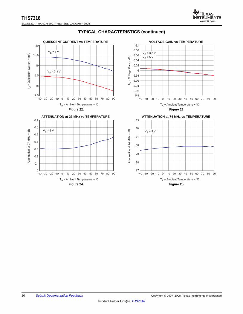
One concern about an active filter in an integrated circuit is the variation of the filter characteristics when theambient temperature and the subsequent die temperature changes. To minimize temperature effects, theTHS7316 uses low temperature coefficient resistors and high quality – low temperature coefficient capacitorsfound in the BiCom-3 process. The filters have been specified by design to account for process variations andtemperature variations to maintain proper filter characteristics. This maintains a low channel-to-channel timedelay which is required for proper video signal performance.
Another benefit of a THS7316 over a passive RLC filter are the input and output impedances. The inputimpedance presented to the DAC varies significantly with a passive network and may cause voltage variationsover frequency. The THS7316 input impedance is 800 kΩ and only the 2-pF input capacitance plus the PCBtrace capacitance impacting the input impedance. As such, the voltage variation appearing at the DAC output isbetter controlled with the THS7316.
On the output side of the filter, a passive filter will again have a impedance variation over frequency. TheTHS7316 is an op-amp which approximates an ideal voltage source. A voltage source is desirable because theoutput impedance is very low and can source and sink current. To properly match the transmission linecharacteristic impedance of a video line, a 75-Ω series resistor is placed on the output. To minimize reflectionsand to maintain a good return loss, this output impedance must maintain a 75-Ω impedance. A passive filterimpedance variation is not specified while the THS7316 has approximately 0.5-Ω of output impedance at10 MHz. Thus, the system is matched better with a THS7316 compared to a passive filter.
One last benefit of the THS7316 over a passive filter is power dissipation. A DAC driving a video line must beable to drive a 37.5-Ω load - the receiver 75-Ω resistor and the 75-Ω impedance matching resistor next to theDAC to maintain the source impedance requirement. This forces the DAC to drive at least 1.25-V peak (100%Saturation CVBS) / 37.5 Ω = 33.3 mA. A DAC is a current steering element and this amount of current flowsinternally to the DAC even if the output is 0-V. Thus, power dissipation in the DAC may be high - especially when6-channels are being driven. Using the THS7316, with a high input impedance and the capability to drive up to2-video lines per channel, can reduce the DAC power dissipation significantly. This is because the resistance theDAC is driving can be substantially increased. It is common to set this in a DAC by a current setting resistor onthe DAC. Thus, the resistance can be 300-Ω or more - substantially reducing the current drive demands from theDAC and saving substantial amount of power. For example, a 3.3-V 6-Channel DAC dissipates 660 mW just forthe steering current capability (6 ch x 33.3 mA x 3.3 V) if it needs to drive 37.5-Ω load. With a 300-Ω load, theDAC power dissipation due to current steering current would only be 82.5 mW (6 ch X 4.16 mA X 3.3 V).
To evaluate the THS7316, an evaluation module (EVM) is available. This allows for testing of the THS7316 inmany different systems. Inputs and outputs include RCA connectors for consumer grade interconnections, orBNC connectors for higher level lab grade connections. Several unpopulated component pads are found on theEVM to allow for different input and output configurations as dictated by the user.
Figure 33 shows the schematic of the THS7316 EVM. Figure 34 and Figure 35 shows the top layer and bottomlayer of the EVM which incorporates standard high-speed layout practices. The bill of materials is shown inTable 1 as supplied from Texas Instruments.
EVALUATION BOARD/KIT IMPORTANT NOTICETexas Instruments (TI) provides the enclosed product(s) under the following conditions:This evaluation board/kit is intended for use for ENGINEERING DEVELOPMENT, DEMONSTRATION, OR EVALUATION PURPOSESONLY and is not considered by TI to be a finished end-product fit for general consumer use. Persons handling the product(s) must haveelectronics training and observe good engineering practice standards. As such, the goods being provided are not intended to be completein terms of required design-, marketing-, and/or manufacturing-related protective considerations, including product safety and environmentalmeasures typically found in end products that incorporate such semiconductor components or circuit boards. This evaluation board/kit doesnot fall within the scope of the European Union directives regarding electromagnetic compatibility, restricted substances (RoHS), recycling(WEEE), FCC, CE or UL, and therefore may not meet the technical requirements of these directives or other related directives.Should this evaluation board/kit not meet the specifications indicated in the User’s Guide, the board/kit may be returned within 30 days fromthe date of delivery for a full refund. THE FOREGOING WARRANTY IS THE EXCLUSIVE WARRANTY MADE BY SELLER TO BUYERAND IS IN LIEU OF ALL OTHER WARRANTIES, EXPRESSED, IMPLIED, OR STATUTORY, INCLUDING ANY WARRANTY OFMERCHANTABILITY OR FITNESS FOR ANY PARTICULAR PURPOSE.The user assumes all responsibility and liability for proper and safe handling of the goods. Further, the user indemnifies TI from all claimsarising from the handling or use of the goods. Due to the open construction of the product, it is the user’s responsibility to take any and allappropriate precautions with regard to electrostatic discharge.EXCEPT TO THE EXTENT OF THE INDEMNITY SET FORTH ABOVE, NEITHER PARTY SHALL BE LIABLE TO THE OTHER FOR ANYINDIRECT, SPECIAL, INCIDENTAL, OR CONSEQUENTIAL DAMAGES.TI currently deals with a variety of customers for products, and therefore our arrangement with the user is not exclusive.
www.ti.comTHS7316SLOS521A–MARCH 2007–REVISED JANUARY 2008
EVALUATION BOARD/KIT IMPORTANT NOTICE (continued)TI assumes no liability for applications assistance, customer product design, software performance, or infringement of patents orservices described herein.Please read the User’s Guide and, specifically, the Warnings and Restrictions notice in the User’s Guide prior to handling the product. Thisnotice contains important safety information about temperatures and voltages. For additional information on TI’s environmental and/orsafety programs, please contact the TI application engineer or visit www.ti.com/esh.No license is granted under any patent right or other intellectual property right of TI covering or relating to any machine, process, orcombination in which such TI products or services might be or are used.
FCC WarningThis evaluation board/kit is intended for use for ENGINEERING DEVELOPMENT, DEMONSTRATION, OR EVALUATION PURPOSESONLY and is not considered by TI to be a finished end-product fit for general consumer use. It generates, uses, and can radiate radiofrequency energy and has not been tested for compliance with the limits of computing devices pursuant to part 15 of FCC rules, which aredesigned to provide reasonable protection against radio frequency interference. Operation of this equipment in other environments maycause interference with radio communications, in which case the user at his own expense will be required to take whatever measures maybe required to correct this interference.
EVM WARNINGS AND RESTRICTIONSIt is important to operate this EVM within the input voltage range of 2.85 V to 5.5 V single supply and the output voltage range of 0 V to 5.5V.Exceeding the specified input range may cause unexpected operation and/or irreversible damage to the EVM. If there are questionsconcerning the input range, please contact a TI field representative prior to connecting the input power.Applying loads outside of the specified output range may result in unintended operation and/or possible permanent damage to the EVM.Please consult the EVM User's Guide prior to connecting any load to the EVM output. If there is uncertainty as to the load specification,please contact a TI field representative.During normal operation, some circuit components may have case temperatures greater than 85C. The EVM is designed to operateproperly with certain components above 85C as long as the input and output ranges are maintained. These components include but are notlimited to linear regulators, switching transistors, pass transistors, and current sense resistors. These types of devices can be identifiedusing the EVM schematic located in the EVM User's Guide. When placing measurement probes near these devices during operation,please be aware that these devices may be very warm to the touch.
HPA00191DR ACTIVE SOIC D 8 2500 Green (RoHS& no Sb/Br)
CU NIPDAU Level-2-260C-1 YEAR -40 to 85 7316
THS7316D ACTIVE SOIC D 8 75 Green (RoHS& no Sb/Br)
CU NIPDAU Level-2-260C-1 YEAR -40 to 85 7316
THS7316DG4 ACTIVE SOIC D 8 75 Green (RoHS& no Sb/Br)
CU NIPDAU Level-2-260C-1 YEAR -40 to 85 7316
THS7316DR ACTIVE SOIC D 8 2500 Green (RoHS& no Sb/Br)
CU NIPDAU Level-2-260C-1 YEAR -40 to 85 7316
THS7316DRG4 ACTIVE SOIC D 8 2500 Green (RoHS& no Sb/Br)
CU NIPDAU Level-2-260C-1 YEAR -40 to 85 7316
(1) The marketing status values are defined as follows:ACTIVE: Product device recommended for new designs.LIFEBUY: TI has announced that the device will be discontinued, and a lifetime-buy period is in effect.NRND: Not recommended for new designs. Device is in production to support existing customers, but TI does not recommend using this part in a new design.PREVIEW: Device has been announced but is not in production. Samples may or may not be available.OBSOLETE: TI has discontinued the production of the device.
(2) Eco Plan - The planned eco-friendly classification: Pb-Free (RoHS), Pb-Free (RoHS Exempt), or Green (RoHS & no Sb/Br) - please check http://www.ti.com/productcontent for the latest availabilityinformation and additional product content details.TBD: The Pb-Free/Green conversion plan has not been defined.Pb-Free (RoHS): TI's terms "Lead-Free" or "Pb-Free" mean semiconductor products that are compatible with the current RoHS requirements for all 6 substances, including the requirement thatlead not exceed 0.1% by weight in homogeneous materials. Where designed to be soldered at high temperatures, TI Pb-Free products are suitable for use in specified lead-free processes.Pb-Free (RoHS Exempt): This component has a RoHS exemption for either 1) lead-based flip-chip solder bumps used between the die and package, or 2) lead-based die adhesive used betweenthe die and leadframe. The component is otherwise considered Pb-Free (RoHS compatible) as defined above.Green (RoHS & no Sb/Br): TI defines "Green" to mean Pb-Free (RoHS compatible), and free of Bromine (Br) and Antimony (Sb) based flame retardants (Br or Sb do not exceed 0.1% by weightin homogeneous material)
(3) MSL, Peak Temp. - The Moisture Sensitivity Level rating according to the JEDEC industry standard classifications, and peak solder temperature.
(4) There may be additional marking, which relates to the logo, the lot trace code information, or the environmental category on the device.
(5) Multiple Device Markings will be inside parentheses. Only one Device Marking contained in parentheses and separated by a "~" will appear on a device. If a line is indented then it is a continuationof the previous line and the two combined represent the entire Device Marking for that device.
(6) Lead/Ball Finish - Orderable Devices may have multiple material finish options. Finish options are separated by a vertical ruled line. Lead/Ball Finish values may wrap to two lines if the finishvalue exceeds the maximum column width.
Important Information and Disclaimer:The information provided on this page represents TI's knowledge and belief as of the date that it is provided. TI bases its knowledge and belief on informationprovided by third parties, and makes no representation or warranty as to the accuracy of such information. Efforts are underway to better integrate information from third parties. TI has taken andcontinues to take reasonable steps to provide representative and accurate information but may not have conducted destructive testing or chemical analysis on incoming materials and chemicals.TI and TI suppliers consider certain information to be proprietary, and thus CAS numbers and other limited information may not be available for release.
In no event shall TI's liability arising out of such information exceed the total purchase price of the TI part(s) at issue in this document sold by TI to Customer on an annual basis.
Texas Instruments Incorporated (TI) reserves the right to make corrections, enhancements, improvements and other changes to itssemiconductor products and services per JESD46, latest issue, and to discontinue any product or service per JESD48, latest issue. Buyersshould obtain the latest relevant information before placing orders and should verify that such information is current and complete.TI’s published terms of sale for semiconductor products (http://www.ti.com/sc/docs/stdterms.htm) apply to the sale of packaged integratedcircuit products that TI has qualified and released to market. Additional terms may apply to the use or sale of other types of TI products andservices.Reproduction of significant portions of TI information in TI data sheets is permissible only if reproduction is without alteration and isaccompanied by all associated warranties, conditions, limitations, and notices. TI is not responsible or liable for such reproduceddocumentation. Information of third parties may be subject to additional restrictions. Resale of TI products or services with statementsdifferent from or beyond the parameters stated by TI for that product or service voids all express and any implied warranties for theassociated TI product or service and is an unfair and deceptive business practice. TI is not responsible or liable for any such statements.Buyers and others who are developing systems that incorporate TI products (collectively, “Designers”) understand and agree that Designersremain responsible for using their independent analysis, evaluation and judgment in designing their applications and that Designers havefull and exclusive responsibility to assure the safety of Designers' applications and compliance of their applications (and of all TI productsused in or for Designers’ applications) with all applicable regulations, laws and other applicable requirements. Designer represents that, withrespect to their applications, Designer has all the necessary expertise to create and implement safeguards that (1) anticipate dangerousconsequences of failures, (2) monitor failures and their consequences, and (3) lessen the likelihood of failures that might cause harm andtake appropriate actions. Designer agrees that prior to using or distributing any applications that include TI products, Designer willthoroughly test such applications and the functionality of such TI products as used in such applications.TI’s provision of technical, application or other design advice, quality characterization, reliability data or other services or information,including, but not limited to, reference designs and materials relating to evaluation modules, (collectively, “TI Resources”) are intended toassist designers who are developing applications that incorporate TI products; by downloading, accessing or using TI Resources in anyway, Designer (individually or, if Designer is acting on behalf of a company, Designer’s company) agrees to use any particular TI Resourcesolely for this purpose and subject to the terms of this Notice.TI’s provision of TI Resources does not expand or otherwise alter TI’s applicable published warranties or warranty disclaimers for TIproducts, and no additional obligations or liabilities arise from TI providing such TI Resources. TI reserves the right to make corrections,enhancements, improvements and other changes to its TI Resources. TI has not conducted any testing other than that specificallydescribed in the published documentation for a particular TI Resource.Designer is authorized to use, copy and modify any individual TI Resource only in connection with the development of applications thatinclude the TI product(s) identified in such TI Resource. NO OTHER LICENSE, EXPRESS OR IMPLIED, BY ESTOPPEL OR OTHERWISETO ANY OTHER TI INTELLECTUAL PROPERTY RIGHT, AND NO LICENSE TO ANY TECHNOLOGY OR INTELLECTUAL PROPERTYRIGHT OF TI OR ANY THIRD PARTY IS GRANTED HEREIN, including but not limited to any patent right, copyright, mask work right, orother intellectual property right relating to any combination, machine, or process in which TI products or services are used. Informationregarding or referencing third-party products or services does not constitute a license to use such products or services, or a warranty orendorsement thereof. Use of TI Resources may require a license from a third party under the patents or other intellectual property of thethird party, or a license from TI under the patents or other intellectual property of TI.TI RESOURCES ARE PROVIDED “AS IS” AND WITH ALL FAULTS. TI DISCLAIMS ALL OTHER WARRANTIES ORREPRESENTATIONS, EXPRESS OR IMPLIED, REGARDING RESOURCES OR USE THEREOF, INCLUDING BUT NOT LIMITED TOACCURACY OR COMPLETENESS, TITLE, ANY EPIDEMIC FAILURE WARRANTY AND ANY IMPLIED WARRANTIES OFMERCHANTABILITY, FITNESS FOR A PARTICULAR PURPOSE, AND NON-INFRINGEMENT OF ANY THIRD PARTY INTELLECTUALPROPERTY RIGHTS. TI SHALL NOT BE LIABLE FOR AND SHALL NOT DEFEND OR INDEMNIFY DESIGNER AGAINST ANY CLAIM,INCLUDING BUT NOT LIMITED TO ANY INFRINGEMENT CLAIM THAT RELATES TO OR IS BASED ON ANY COMBINATION OFPRODUCTS EVEN IF DESCRIBED IN TI RESOURCES OR OTHERWISE. IN NO EVENT SHALL TI BE LIABLE FOR ANY ACTUAL,DIRECT, SPECIAL, COLLATERAL, INDIRECT, PUNITIVE, INCIDENTAL, CONSEQUENTIAL OR EXEMPLARY DAMAGES INCONNECTION WITH OR ARISING OUT OF TI RESOURCES OR USE THEREOF, AND REGARDLESS OF WHETHER TI HAS BEENADVISED OF THE POSSIBILITY OF SUCH DAMAGES.Unless TI has explicitly designated an individual product as meeting the requirements of a particular industry standard (e.g., ISO/TS 16949and ISO 26262), TI is not responsible for any failure to meet such industry standard requirements.Where TI specifically promotes products as facilitating functional safety or as compliant with industry functional safety standards, suchproducts are intended to help enable customers to design and create their own applications that meet applicable functional safety standardsand requirements. Using products in an application does not by itself establish any safety features in the application. Designers mustensure compliance with safety-related requirements and standards applicable to their applications. Designer may not use any TI products inlife-critical medical equipment unless authorized officers of the parties have executed a special contract specifically governing such use.Life-critical medical equipment is medical equipment where failure of such equipment would cause serious bodily injury or death (e.g., lifesupport, pacemakers, defibrillators, heart pumps, neurostimulators, and implantables). Such equipment includes, without limitation, allmedical devices identified by the U.S. Food and Drug Administration as Class III devices and equivalent classifications outside the U.S.TI may expressly designate certain products as completing a particular qualification (e.g., Q100, Military Grade, or Enhanced Product).Designers agree that it has the necessary expertise to select the product with the appropriate qualification designation for their applicationsand that proper product selection is at Designers’ own risk. Designers are solely responsible for compliance with all legal and regulatoryrequirements in connection with such selection.Designer will fully indemnify TI and its representatives against any damages, costs, losses, and/or liabilities arising out of Designer’s non-compliance with the terms and provisions of this Notice.


![this pagePDF-1.6 %âãÏÓ 75 0 obj endobj 81 0 obj /Filter/FlateDecode/ID[]/Index[75 8]/Info 74 0 R/Length 40/Prev 2036890/Root 76 0 R/Size 83/Type/XRef/W[1 2 0]>>stream](https://static.documents.pub/doc/80x56/5aedb03b7f8b9a45568fffe4/this-page-pdf-16-75-0-obj-endobj-81-0-obj-filterflatedecodeidindex75-8info.jpg)


