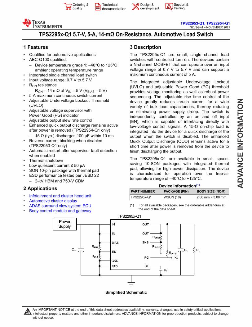
TPS2295x-Q1 5.7-V, 5-A, 14-mΩ On-Resistance, Automotive Load Switch 1 Features • Qualified for automotive applications • AEC-Q100 qualified: – Device temperature grade 1: –40°C to 125°C ambient operating temperature range • Integrated single channel load switch • Input voltage range: 0.7 V to 5.7 V • R ON resistance – R ON = 14 mΩ at V IN = 5 V (V BIAS = 5 V) • 5-A maximum continuous switch current • Adjustable Undervoltage Lockout Threshold (UVLO) • Adjustable voltage supervisor with Power Good (PG) indicator • Adjustable output slew rate control • Enhanced quick output discharge remains active after power is removed (TPS22954-Q1 only) – 15 Ω (typ.) discharges 100 µF within 10 ms • Reverse current blocking when disabled (TPS22953-Q1 only) • Automatic restart after supervisor fault detection when enabled • Thermal shutdown • Low quiescent current ≤ 50 µA • SON 10-pin package with thermal pad • ESD performance tested per JESD 22 – 2-kV HBM and 750-V CDM 2 Applications • Infotainment and cluster head unit • Automotive cluster display • ADAS surround view system ECU • Body control module and gateway 3 Description The TPS2295x-Q1 are small, single channel load switches with controlled turn on. The devices contain a N-channel MOSFET that can operate over an input voltage range of 0.7 V to 5.7 V and can support a maximum continuous current of 5 A. The integrated adjustable Undervoltage Lockout (UVLO) and adjustable Power Good (PG) threshold provides voltage monitoring as well as robust power sequencing. The adjustable rise time control of the device greatly reduces inrush current for a wide variety of bulk load capacitances, thereby reducing or eliminating power supply droop. The switch is independently controlled by an on and off input (EN), which is capable of interfacing directly with low-voltage control signals. A 15-Ω on-chip load is integrated into the device for a quick discharge of the output when the switch is disabled. The enhanced Quick Output Discharge (QOD) remains active for a short time after power is removed from the device to finish discharging the output. The TPS2295x-Q1 are available in small, space- saving 10-SON packages with integrated thermal pad, allowing for high power dissipation. The device is characterized for operation over the free-air temperature range of –40°C to +125°C. Device Information (1) PART NUMBER PACKAGE (PIN) BODY SIZE (NOM) TPS2295x-Q1 WSON (10) 2.00 mm × 3.00 mm (1) For all available packages, see the orderable addendum at the end of the data sheet. Simplified Schematic ADVANCE INFORMATION TPS22953-Q1, TPS22954-Q1 SLVSGK4 – NOVEMBER 2021 An IMPORTANT NOTICE at the end of this data sheet addresses availability, warranty, changes, use in safety-critical applications, intellectual property matters and other important disclaimers. ADVANCE INFORMATION for preproduction products; subject to change without notice.
1 Features• Qualified for automotive applications• AEC-Q100 qualified:
– Device temperature grade 1: –40°C to 125°C ambient operating temperature range
• Integrated single channel load switch• Input voltage range: 0.7 V to 5.7 V• RON resistance
– RON = 14 mΩ at VIN = 5 V (VBIAS = 5 V)• 5-A maximum continuous switch current• Adjustable Undervoltage Lockout Threshold
(UVLO)• Adjustable voltage supervisor with
Power Good (PG) indicator• Adjustable output slew rate control• Enhanced quick output discharge remains active
after power is removed (TPS22954-Q1 only)– 15 Ω (typ.) discharges 100 µF within 10 ms
• Reverse current blocking when disabled (TPS22953-Q1 only)
• Automatic restart after supervisor fault detection when enabled
• Thermal shutdown• Low quiescent current ≤ 50 µA• SON 10-pin package with thermal pad• ESD performance tested per JESD 22
– 2-kV HBM and 750-V CDM
2 Applications• Infotainment and cluster head unit• Automotive cluster display• ADAS surround view system ECU• Body control module and gateway
3 DescriptionThe TPS2295x-Q1 are small, single channel load switches with controlled turn on. The devices contain a N-channel MOSFET that can operate over an input voltage range of 0.7 V to 5.7 V and can support a maximum continuous current of 5 A.
The integrated adjustable Undervoltage Lockout (UVLO) and adjustable Power Good (PG) threshold provides voltage monitoring as well as robust power sequencing. The adjustable rise time control of the device greatly reduces inrush current for a wide variety of bulk load capacitances, thereby reducing or eliminating power supply droop. The switch is independently controlled by an on and off input (EN), which is capable of interfacing directly with low-voltage control signals. A 15-Ω on-chip load is integrated into the device for a quick discharge of the output when the switch is disabled. The enhanced Quick Output Discharge (QOD) remains active for a short time after power is removed from the device to finish discharging the output.
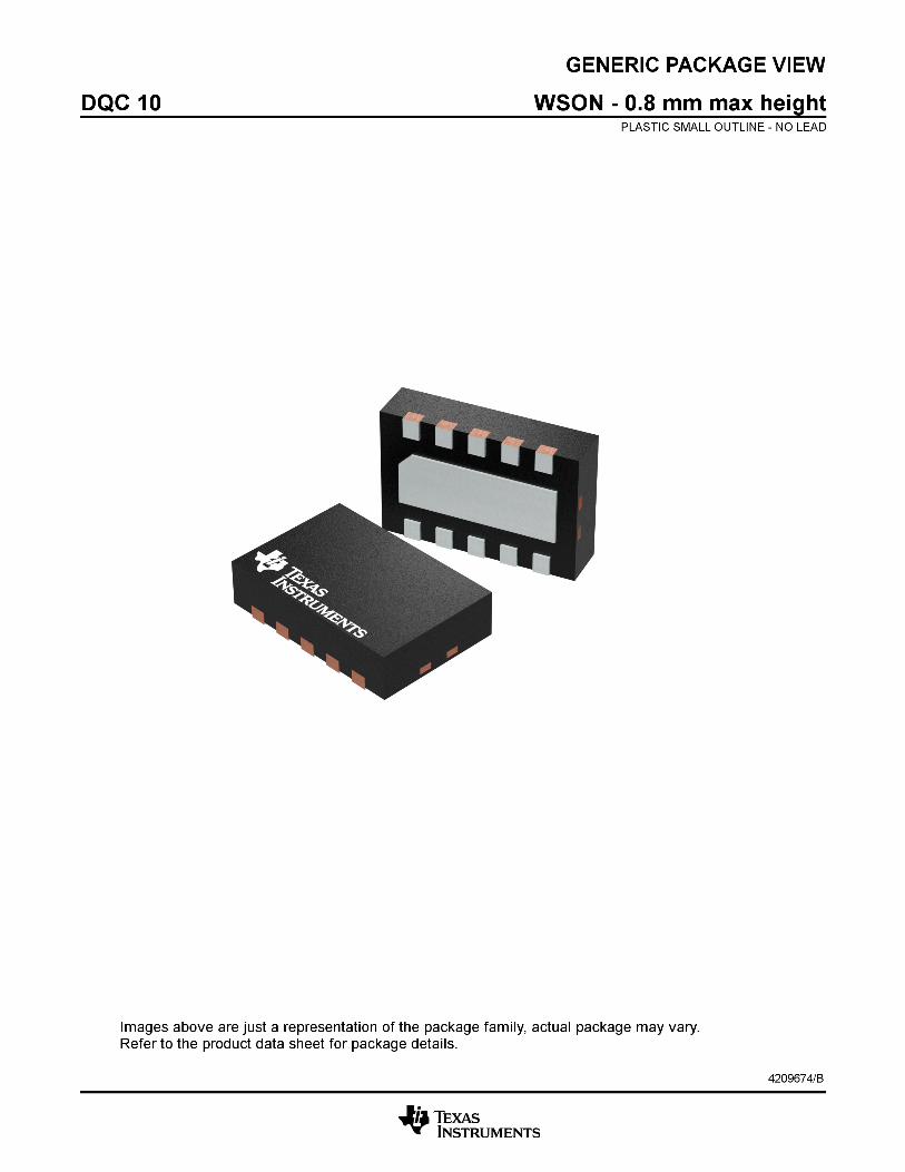
The TPS2295x-Q1 are available in small, space-saving 10-SON packages with integrated thermal pad, allowing for high power dissipation. The device is characterized for operation over the free-air temperature range of –40°C to +125°C.
Device Information(1)
PART NUMBER PACKAGE (PIN) BODY SIZE (NOM)TPS2295x-Q1 WSON (10) 2.00 mm × 3.00 mm
(1) For all available packages, see the orderable addendum at the end of the data sheet.
Simplified Schematic
AD
VAN
CE
INFO
RM
ATIO
N
TPS22953-Q1, TPS22954-Q1SLVSGK4 – NOVEMBER 2021
An IMPORTANT NOTICE at the end of this data sheet addresses availability, warranty, changes, use in safety-critical applications, intellectual property matters and other important disclaimers. ADVANCE INFORMATION for preproduction products; subject to change without notice.
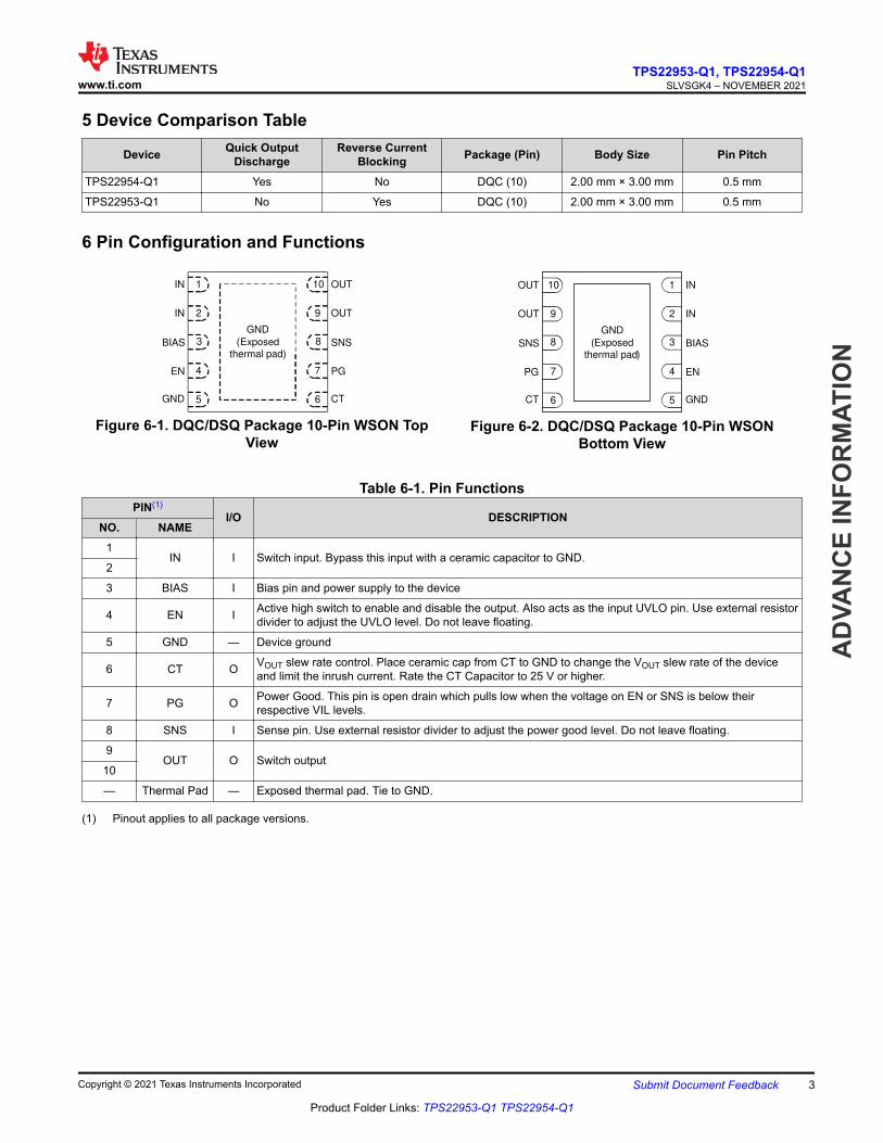
1IN I Switch input. Bypass this input with a ceramic capacitor to GND.
2
3 BIAS I Bias pin and power supply to the device
4 EN I Active high switch to enable and disable the output. Also acts as the input UVLO pin. Use external resistor divider to adjust the UVLO level. Do not leave floating.
5 GND — Device ground
6 CT O VOUT slew rate control. Place ceramic cap from CT to GND to change the VOUT slew rate of the device and limit the inrush current. Rate the CT Capacitor to 25 V or higher.
7 PG O Power Good. This pin is open drain which pulls low when the voltage on EN or SNS is below their respective VIL levels.
8 SNS I Sense pin. Use external resistor divider to adjust the power good level. Do not leave floating.
7 Specifications7.1 Absolute Maximum RatingsOver operating free-air temperature range (unless otherwise noted)(1)
MIN MAX UNIT
VIN Input voltage –0.3 6 V
VBIAS Bias voltage –0.3 6 V
VOUT Output voltage –0.3 6 V
VEN, VSNS, VPG EN, SNS, and PG voltage –0.3 6 V
IMAX Maximum continuous switch current, TA = 70°C 5 A
IPLS Maximum pulsed switch current, pulse < 300-µs, 2% duty cycle 7 A
TJ Maximum junction temperature Internally Limited
Tstg Storage temperature –65 150 °C
(1) Operation outside the Absolute Maximum Ratings may cause permanent device damage. Absolute Maximum Ratings do not imply functional operation of the device at these or any other conditions beyond those listed under Recommended Operating Conditions. If used outside the Recommended Operating Conditions but within the Absolute Maximum Ratings, the device may not be fully functional, and this may affect device reliability, functionality, performance, and shorten the device lifetime.
7.2 ESD RatingsVALUE UNIT
V(ESD) Electrostatic discharge
Human body model (HBM), per AEC Q100- 002(1)
HBM ESD classification level 2 ±2000V
Charged device model (CDM), per AEC Q100- 011CDM ESD classification level C5 ±750
(1) AEC Q100-002 indicates that HBM stressing shall be in accordance with the ANSI/ESDA/JEDEC JS-001 specification.
Recommended Operating Conditionsover operating free-air temperature range (unless otherwise noted)
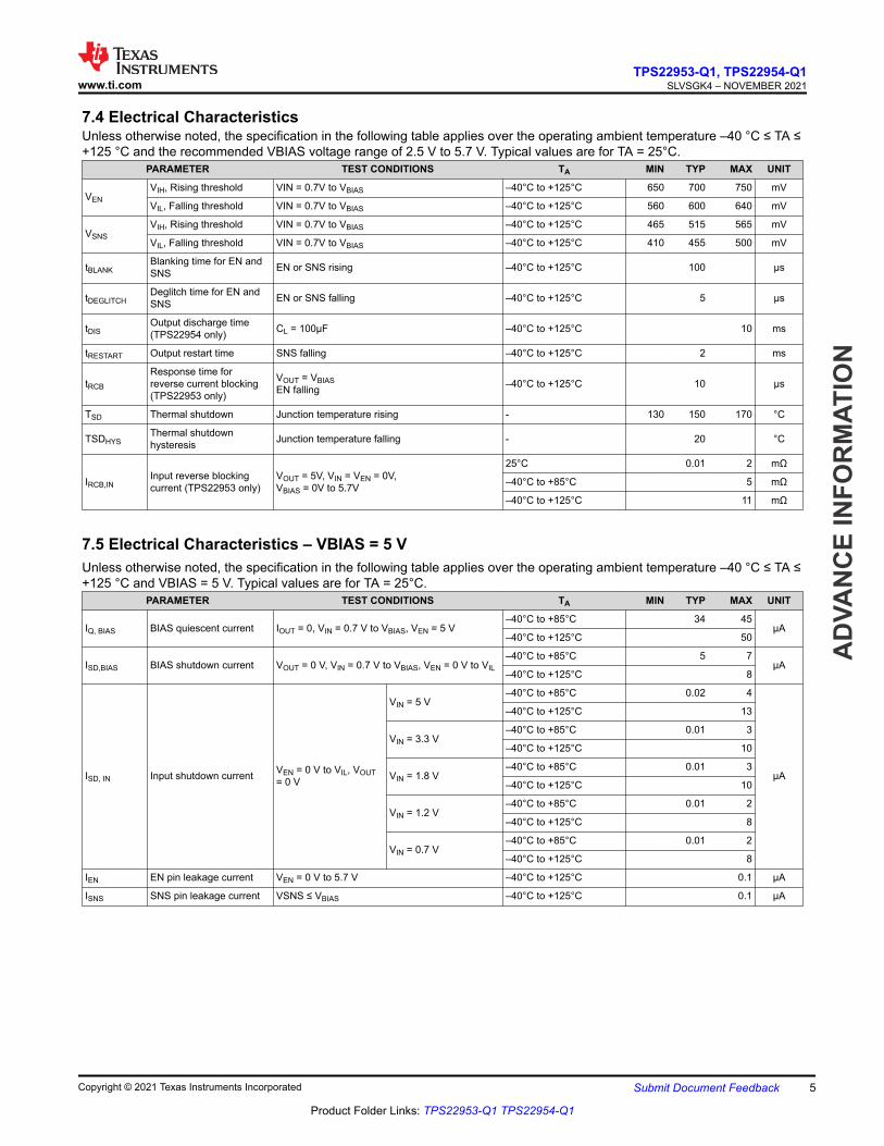
7.4 Electrical CharacteristicsUnless otherwise noted, the specification in the following table applies over the operating ambient temperature –40 °C ≤ TA ≤ +125 °C and the recommended VBIAS voltage range of 2.5 V to 5.7 V. Typical values are for TA = 25°C.
PARAMETER TEST CONDITIONS TA MIN TYP MAX UNIT
VENVIH, Rising threshold VIN = 0.7V to VBIAS –40°C to +125°C 650 700 750 mV
VIL, Falling threshold VIN = 0.7V to VBIAS –40°C to +125°C 560 600 640 mV
VSNSVIH, Rising threshold VIN = 0.7V to VBIAS –40°C to +125°C 465 515 565 mV
VIL, Falling threshold VIN = 0.7V to VBIAS –40°C to +125°C 410 455 500 mV
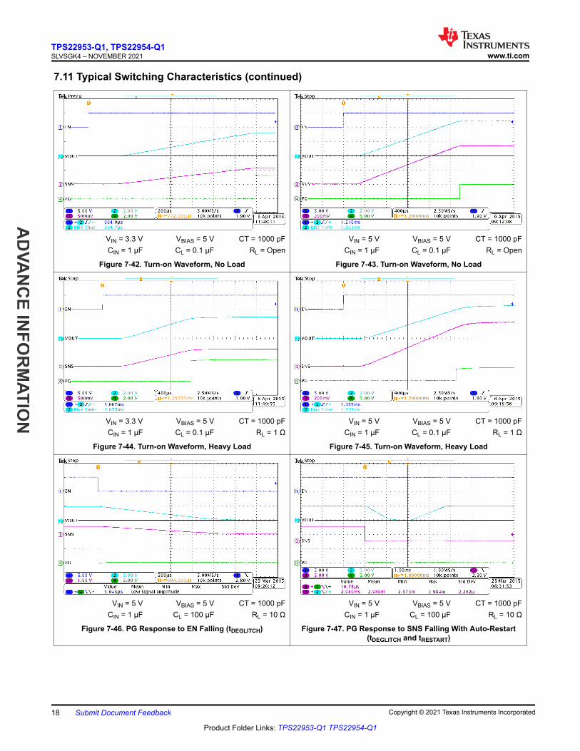
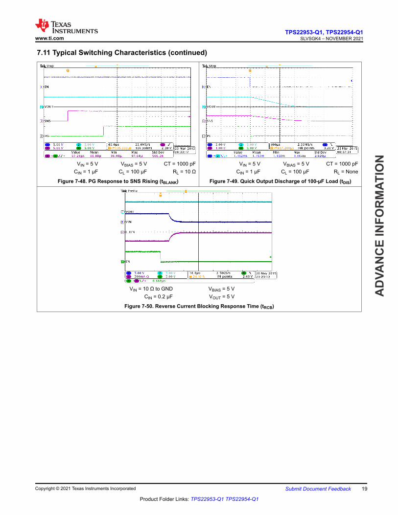
tBLANKBlanking time for EN and SNS EN or SNS rising –40°C to +125°C 100 µs
tDEGLITCHDeglitch time for EN and SNS EN or SNS falling –40°C to +125°C 5 µs
tDISOutput discharge time (TPS22954 only) CL = 100µF –40°C to +125°C 10 ms
tRESTART Output restart time SNS falling –40°C to +125°C 2 ms
tRCB
Response time for reverse current blocking (TPS22953 only)
VOUT = VBIASEN falling –40°C to +125°C 10 µs
TSD Thermal shutdown Junction temperature rising - 130 150 170 °C
TSDHYSThermal shutdown hysteresis Junction temperature falling - 20 °C
IRCB,INInput reverse blocking current (TPS22953 only)
VOUT = 5V, VIN = VEN = 0V,VBIAS = 0V to 5.7V
25°C 0.01 2 mΩ
–40°C to +85°C 5 mΩ
–40°C to +125°C 11 mΩ
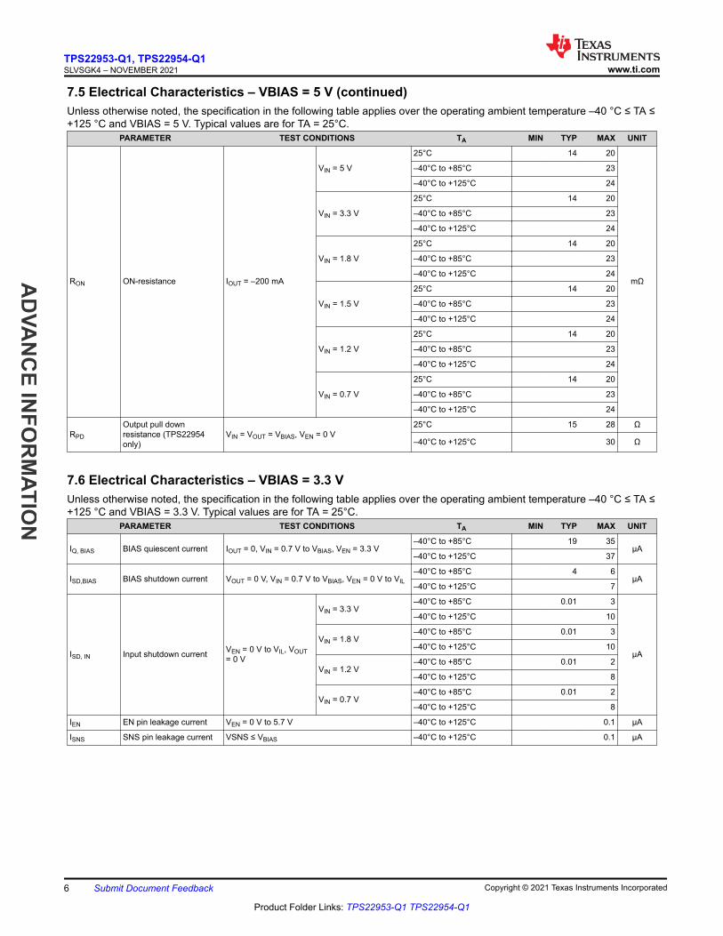
7.5 Electrical Characteristics – VBIAS = 5 VUnless otherwise noted, the specification in the following table applies over the operating ambient temperature –40 °C ≤ TA ≤ +125 °C and VBIAS = 5 V. Typical values are for TA = 25°C.
PARAMETER TEST CONDITIONS TA MIN TYP MAX UNIT
IQ, BIAS BIAS quiescent current IOUT = 0, VIN = 0.7 V to VBIAS, VEN = 5 V–40°C to +85°C 34 45
µA–40°C to +125°C 50
ISD,BIAS BIAS shutdown current VOUT = 0 V, VIN = 0.7 V to VBIAS, VEN = 0 V to VIL–40°C to +85°C 5 7
µA–40°C to +125°C 8
ISD, IN Input shutdown current VEN = 0 V to VIL, VOUT = 0 V
VIN = 5 V–40°C to +85°C 0.02 4
µA
–40°C to +125°C 13
VIN = 3.3 V–40°C to +85°C 0.01 3
–40°C to +125°C 10
VIN = 1.8 V–40°C to +85°C 0.01 3
–40°C to +125°C 10
VIN = 1.2 V–40°C to +85°C 0.01 2
–40°C to +125°C 8
VIN = 0.7 V–40°C to +85°C 0.01 2
–40°C to +125°C 8
IEN EN pin leakage current VEN = 0 V to 5.7 V –40°C to +125°C 0.1 µA
ISNS SNS pin leakage current VSNS ≤ VBIAS –40°C to +125°C 0.1 µA
7.5 Electrical Characteristics – VBIAS = 5 V (continued)Unless otherwise noted, the specification in the following table applies over the operating ambient temperature –40 °C ≤ TA ≤ +125 °C and VBIAS = 5 V. Typical values are for TA = 25°C.
PARAMETER TEST CONDITIONS TA MIN TYP MAX UNIT
RON ON-resistance IOUT = –200 mA
VIN = 5 V
25°C 14 20
mΩ
–40°C to +85°C 23
–40°C to +125°C 24
VIN = 3.3 V
25°C 14 20
–40°C to +85°C 23
–40°C to +125°C 24
VIN = 1.8 V
25°C 14 20
–40°C to +85°C 23
–40°C to +125°C 24
VIN = 1.5 V
25°C 14 20
–40°C to +85°C 23
–40°C to +125°C 24
VIN = 1.2 V
25°C 14 20
–40°C to +85°C 23
–40°C to +125°C 24
VIN = 0.7 V
25°C 14 20
–40°C to +85°C 23
–40°C to +125°C 24
RPD
Output pull down resistance (TPS22954 only)
VIN = VOUT = VBIAS, VEN = 0 V25°C 15 28 Ω
–40°C to +125°C 30 Ω
7.6 Electrical Characteristics – VBIAS = 3.3 VUnless otherwise noted, the specification in the following table applies over the operating ambient temperature –40 °C ≤ TA ≤ +125 °C and VBIAS = 3.3 V. Typical values are for TA = 25°C.
PARAMETER TEST CONDITIONS TA MIN TYP MAX UNIT
IQ, BIAS BIAS quiescent current IOUT = 0, VIN = 0.7 V to VBIAS, VEN = 3.3 V–40°C to +85°C 19 35
µA–40°C to +125°C 37
ISD,BIAS BIAS shutdown current VOUT = 0 V, VIN = 0.7 V to VBIAS, VEN = 0 V to VIL–40°C to +85°C 4 6
µA–40°C to +125°C 7
ISD, IN Input shutdown current VEN = 0 V to VIL, VOUT = 0 V
VIN = 3.3 V–40°C to +85°C 0.01 3
µA
–40°C to +125°C 10
VIN = 1.8 V–40°C to +85°C 0.01 3
–40°C to +125°C 10
VIN = 1.2 V–40°C to +85°C 0.01 2
–40°C to +125°C 8
VIN = 0.7 V–40°C to +85°C 0.01 2
–40°C to +125°C 8
IEN EN pin leakage current VEN = 0 V to 5.7 V –40°C to +125°C 0.1 µA
ISNS SNS pin leakage current VSNS ≤ VBIAS –40°C to +125°C 0.1 µA
TPS22953-Q1, TPS22954-Q1SLVSGK4 – NOVEMBER 2021 www.ti.com
7.6 Electrical Characteristics – VBIAS = 3.3 V (continued)Unless otherwise noted, the specification in the following table applies over the operating ambient temperature –40 °C ≤ TA ≤ +125 °C and VBIAS = 3.3 V. Typical values are for TA = 25°C.
PARAMETER TEST CONDITIONS TA MIN TYP MAX UNIT
RON ON-resistance IOUT = –200 mA
VIN = 3.3 V
25°C 15 21
mΩ
–40°C to +85°C 24
–40°C to +125°C 25
VIN = 1.8 V
25°C 14 20
–40°C to +85°C 23
–40°C to +125°C 24
VIN = 1.5 V
25°C 14 20
–40°C to +85°C 23
–40°C to +125°C 24
VIN = 1.2 V
25°C 14 20
–40°C to +85°C 23
–40°C to +125°C 24
VIN = 0.7 V
25°C 14 20
–40°C to +85°C 23
–40°C to +125°C 24
RPD
Output pull down resistance (TPS22954 only)
VIN = VOUT = VBIAS, VEN = 0 V25°C 13 28 Ω
–40°C to +125°C 30 Ω
7.7 Electrical Characteristics – VBIAS = 2.5 VUnless otherwise noted, the specification in the following table applies over the operating ambient temperature –40 °C ≤ TA ≤ +125 °C and VBIAS = 2.5 V. Typical values are for TA = 25°C.
PARAMETER TEST CONDITIONS TA MIN TYP MAX UNIT
IQ, BIAS BIAS quiescent current IOUT = 0, VIN = 0.7 V to VBIAS, VEN = 2.5 V–40°C to +85°C 16 25
µA–40°C to +125°C 27
ISD,BIAS BIAS shutdown current VOUT = 0 V, VIN = 0.7 V to VBIAS, VEN = 0 V to VIL–40°C to +85°C 4 5
µA–40°C to +125°C 6
ISD, IN Input shutdown current VEN = 0 V to VIL, VOUT = 0 V
VIN = 2.5 V–40°C to +85°C 0.01 3
µA
–40°C to +125°C 10
VIN = 1.8 V–40°C to +85°C 0.01 3
–40°C to +125°C 10
VIN = 1.2 V–40°C to +85°C 0.01 2
–40°C to +125°C 8
VIN = 0.7 V–40°C to +85°C 0.01 2
–40°C to +125°C 8
IEN EN pin leakage current VEN = 0 V to 5.7V –40°C to +125°C 0.1 µA
ISNS SNS pin leakage current VSNS ≤ VBIAS –40°C to +125°C 0.1 µA
7.7 Electrical Characteristics – VBIAS = 2.5 V (continued)Unless otherwise noted, the specification in the following table applies over the operating ambient temperature –40 °C ≤ TA ≤ +125 °C and VBIAS = 2.5 V. Typical values are for TA = 25°C.
PARAMETER TEST CONDITIONS TA MIN TYP MAX UNIT
RON ON-resistance IOUT = –200 mA
VIN = 2.5 V
25°C 16 23
mΩ
–40°C to +85°C 26
–40°C to +125°C 27
VIN = 1.8 V
25°C 15 22
–40°C to +85°C 25
–40°C to +125°C 26
VIN = 1.5 V
25°C 15 22
–40°C to +85°C 25
–40°C to +125°C 26
VIN = 1.2 V
25°C 15 22
–40°C to +85°C 24
–40°C to +125°C 25
VIN = 0.7 V
25°C 14 21
–40°C to +85°C 24
–40°C to +125°C 25
RPD
Output pull down resistance (TPS22954 only)
VIN = VOUT = VBIAS, VEN = 0 V25°C 12 28 Ω
–40°C to +125°C 30 Ω
TPS22953-Q1, TPS22954-Q1SLVSGK4 – NOVEMBER 2021 www.ti.com
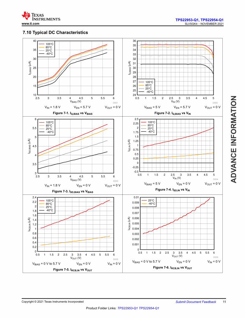
9 Detailed Description9.1 OverviewThe TPS2295x-Q1 are 5.7-V, 5-A load switches in 10-pin SON packages. To reduce voltage drop for low voltage, high current rails the device implements a low-resistance N-channel MOSFET, which reduces the drop out voltage through the device at high currents. The integrated adjustable Undervoltage Lockout (UVLO) and adjustable Power Good (PG) threshold provides voltage monitoring as well as robust power sequencing.
The adjustable rise time control of the device greatly reduces inrush current for a wide variety of bulk load capacitances, thereby reducing or eliminating power supply droop. The switch is independently controlled by an on and off input (EN), which is capable of interfacing directly with low-voltage control signals. A 15-Ω on-chip load resistor integrates into the device for output quick discharge when the switch turns off.
During shutdown, the device has very low leakage currents, thereby reducing unnecessary leakages for downstream modules during standby. Integrated power monitoring functionality, control logic, driver, power supply, and output discharge FET eliminates the need for any external components, which reduces solution size and BOM count.
9.3 Feature Description9.3.1 On and Off Control (EN pin)
The EN pin controls the state of the switch. When the voltage on EN exceeds VIH,EN the switch enables. When EN goes below VIL,EN the switch disables.
The EN pin has a blanking time of tBLANK on the rising edge once the VIH,EN threshold has been exceeded. The EN pin also has a de-glitch time of tDEGLITCH when the voltage has gone below VIL,EN.
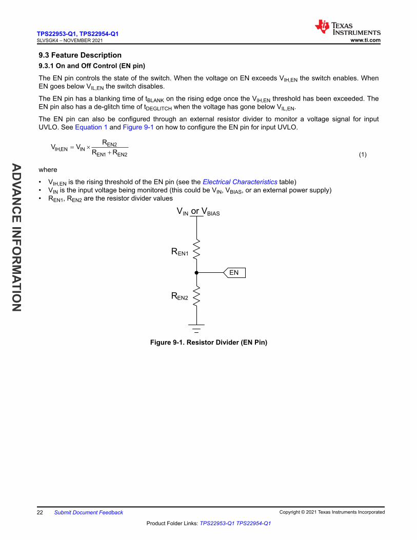
The EN pin can also be configured through an external resistor divider to monitor a voltage signal for input UVLO. See Equation 1 and Figure 9-1 on how to configure the EN pin for input UVLO.
EN2IH,EN IN
EN1 EN2
RV V
R R= ´
+ (1)
where
• VIH,EN is the rising threshold of the EN pin (see the Electrical Characteristics table)• VIN is the input voltage being monitored (this could be VIN, VBIAS, or an external power supply)• REN1, REN2 are the resistor divider values
VIN or VBIAS
REN1
REN2
EN
Figure 9-1. Resistor Divider (EN Pin)
TPS22953-Q1, TPS22954-Q1SLVSGK4 – NOVEMBER 2021 www.ti.com
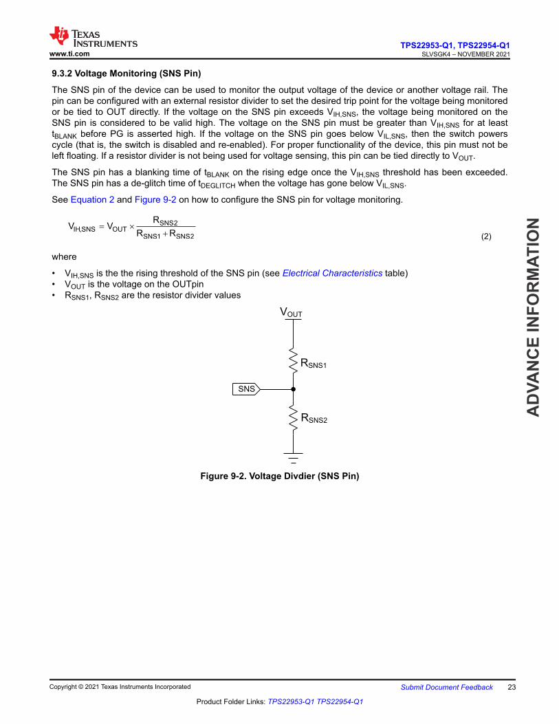
The SNS pin of the device can be used to monitor the output voltage of the device or another voltage rail. The pin can be configured with an external resistor divider to set the desired trip point for the voltage being monitored or be tied to OUT directly. If the voltage on the SNS pin exceeds VIH,SNS, the voltage being monitored on the SNS pin is considered to be valid high. The voltage on the SNS pin must be greater than VIH,SNS for at least tBLANK before PG is asserted high. If the voltage on the SNS pin goes below VIL,SNS, then the switch powers cycle (that is, the switch is disabled and re-enabled). For proper functionality of the device, this pin must not be left floating. If a resistor divider is not being used for voltage sensing, this pin can be tied directly to VOUT.
The SNS pin has a blanking time of tBLANK on the rising edge once the VIH,SNS threshold has been exceeded. The SNS pin has a de-glitch time of tDEGLITCH when the voltage has gone below VIL,SNS.
See Equation 2 and Figure 9-2 on how to configure the SNS pin for voltage monitoring.
SNS2IH,SNS OUT
SNS1 SNS2
RV V
R R= ´
+ (2)
where
• VIH,SNS is the the rising threshold of the SNS pin (see Electrical Characteristics table)• VOUT is the voltage on the OUTpin• RSNS1, RSNS2 are the resistor divider values
The PG pin is only asserted high when the voltage on EN exceeds VIH,EN and the voltage on SNS exceeds VIH,SNS. There is a tBLANK time, typically 100 µs, between the SNS voltage exceeding VIH,SNS and PG being asserted high. If the voltage on EN goes below VIL,EN or the voltage on SNS goes below VIL,SNS, PG is de-asserted. There is a tDEGLITCH time, typically 5µs, between the EN voltage or SNS voltage going below their respective VIL levels and PG being pulled low.
PG is an open drain pin and must be pulled up with a pull-up resistor. Be sure to never exceed the maximum operating voltage on this pin. If PG is not being used in the application, tie it to GND for proper device functionality.
For proper PG operation, the BIAS voltage must be within the recommended operating range. In systems that are very sensitive to noise or have long PG traces, TI recommends to add a small capacitance from PG to GND for decoupling.
9.3.4 Supervisor Fault Detection and Automatic Restart
The falling edge of the SNS pin below VIL,SNS is considered a fault case and causes the load switch to be disabled for tRESTART (typically 2 ms). After the tRESTART time, the switch is automatically re-enabled as long as EN is still above VIH,EN. In the case the SNS pin is being used to monitor VOUT or a downstream voltage, the restart helps to protect against excessive overcurrent if there is a quick short to GND. See Figure 9-3.
IN
BIAS
EN
SNS VIL,SNS
OUT
PG
tDEGLITCH
tRESTART
Voltage
Pulled
Down
VIH,SNS
tBLANK
tD
10%
90%
tR
VIN
VBIAS
0
0
0
VEN
VOUT
0
VSNS
0
0
VPG
Time
Figure 9-3. Automatic Restart After Quick Short to GND
TPS22953-Q1, TPS22954-Q1SLVSGK4 – NOVEMBER 2021 www.ti.com
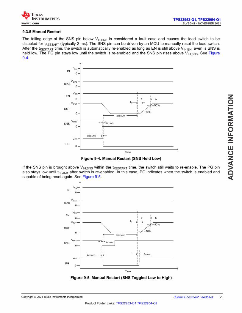
The falling edge of the SNS pin below VIL,SNS is considered a fault case and causes the load switch to be disabled for tRESTART (typically 2 ms). The SNS pin can be driven by an MCU to manually reset the load switch. After the tRESTART time, the switch is automatically re-enabled as long as EN is still above VIH,EN, even is SNS is held low. The PG pin stays low until the switch is re-enabled and the SNS pin rises above VIH,SNS. See Figure 9-4.
VIL,SNS
tDEGLITCH
tRESTART
tD
10%
90%
tR
IN
BIAS
EN
SNS
OUT
PG
VIN
VBIAS
0
0
0
VEN
VOUT
0
VSNS
0
0
VPG
Time
Figure 9-4. Manual Restart (SNS Held Low)
If the SNS pin is brought above VIH,SNS within the tRESTART time, the switch still waits to re-enable. The PG pin also stays low until tBLANK after switch is re-enabled. In this case, PG indicates when the switch is enabled and capable of being reset again. See Figure 9-5.
VIL,SNS
tDEGLITCH
tRESTART
tD
10%
90%
tR
tBLANK
IN
BIAS
EN
SNS
OUT
PG
VIN
VBIAS
0
0
0
VEN
VOUT
0
VSNS
0
0
VPG
Time
Figure 9-5. Manual Restart (SNS Toggled Low to High)
If the junction temperature of the device exceeds TSD, the switch disables. The device enables after the junction temperature drops by TSDHYS as long as EN is still greater than VIH,EN.
9.3.7 Reverse Current Blocking (TPS22953-Q1 Only)
When the switch disables (either by de-asserting EN or SNS, triggering thermal shutdown, or losing power), the reverse current blocking (RCB) feature of the device engages within tRCB, typically 10 μs. After the RCB engages, the reverse current from the OUT pin to the IN pin is limited to IRCB,IN, typically 0.01 μA.
The Quick Output Discharge (QOD) transistor is engaged indefinitely whenever the switch is disabled and the recommended VBIAS voltage is met. During this state, the QOD resistance (RPD) discharges VOUT to GND. TI does not recommend to apply a continuous DC voltage to OUT when the device is disabled.
The QOD transistor can remain active for a short period of time even after VBIAS loses power. This brief period of time is defined as tDIS. For best results, TI recommends the device get disabled before VBIAS goes below the minimum recommended voltage. The waveform in Figure 9-6 shows the behavior when power is applied and then removed in a typical application.
VIH,SNS VIL,SNS
VIH,EN
tBLANK
VIL,EN
tDEGLITCH
tBLANK
VOUT < 100mV
tDEGLITCH
tDIS
IN
BIAS
EN
SNS
OUT
PG
VIN
VBIAS
0
0
0
VEN
VOUT
0
VSNS
0
0
VPG
Time
Figure 9-6. Power Applied and Then Removed in a Typical Application
At the end of the tDIS time, it is not guaranteed that VOUT will be 0 V because the final voltage is dependent upon the initial voltage and the CL capacitor. The final VOUT can be calculated with Equation 3 for a given initial voltage and CL capacitor.
t
RCƒ oV V e
-
= ´ (3)
where
• Vf is the final VOUT voltage• Vo is the initial VOUT voltage• R is the the value of the output discharge resistor, RPD (see the Electrical Characteristics table)• C is the output bulk capacitance on OUT
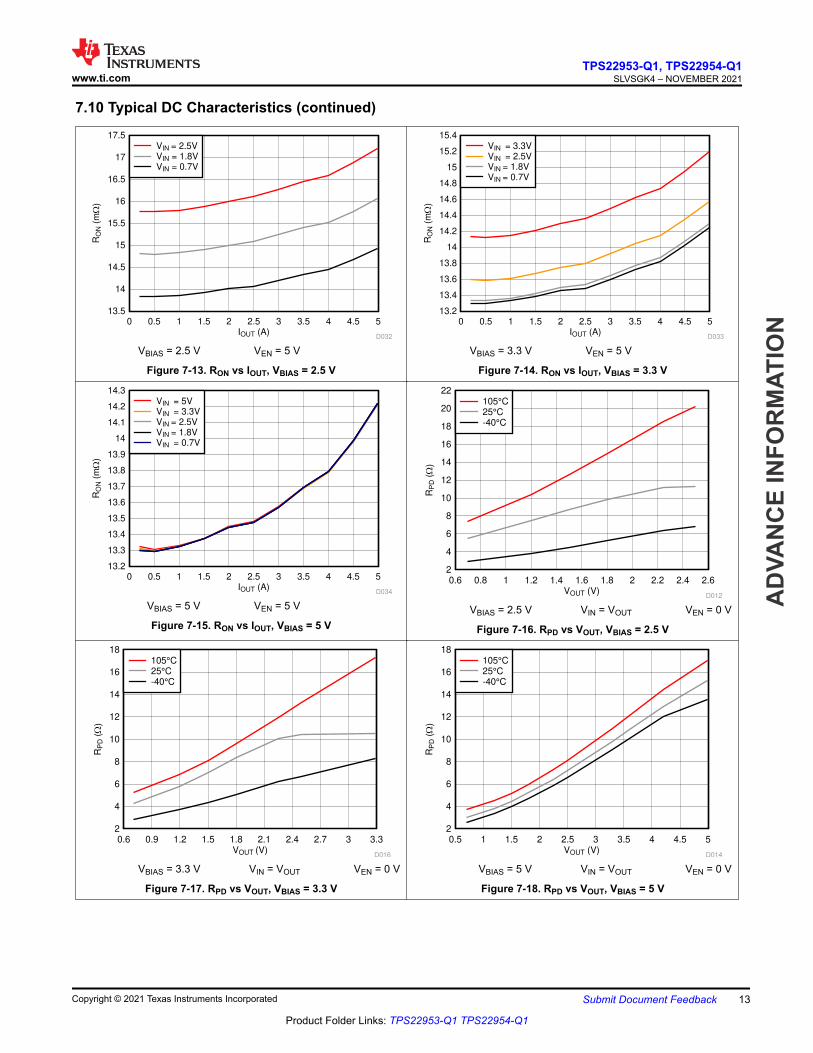
9.3.9 VIN and VBIAS Voltage Range
For optimal RON performance, make sure VIN ≤ VBIAS. The device is still functional if VIN > VBIAS but it exhibits RON greater than what is listed in the Electrical Characteristics table. See Figure 9-7 for an example of a typical
TPS22953-Q1, TPS22954-Q1SLVSGK4 – NOVEMBER 2021 www.ti.com
device. Notice the increasing RON as VIN increases. Be sure to never exceed the maximum voltage rating for VIN and VBIAS.
VIN (V)
RO
N (
m:
)
0.5 1 1.5 2 2.5 3 3.5 4 4.5 5 5.5 610
15
20
25
30
35
40
45
50
55
D031
VBIAS = 2.5VVBIAS = 3.3VVBIAS = 5VVBIAS = 5.7V
Figure 9-7. RON When VIN > VBIAS
9.3.10 Adjustable Rise Time (CT Pin)
A capacitor to GND on the CT pin sets the slew rate for VOUT. An appropriate capacitance value must be placed on CT such that the IMAX and IPLS specifications of the device are not violated. The capacitor to GND on the CT pin must be rated for 25 V or higher. Equation 4 shows an approximate formula for the relationship between CT (except for CT = open) and the slew rate for any VBIAS.
SR = 0.35 × CT + 20 (4)
where
• SR is the slew rate (in μs/V)• CT is the the capacitance value on the CT terminal (in pF)• The units for the constant 20 are μs/V.• The units for the constant 0.35 are μs/(V*pF).
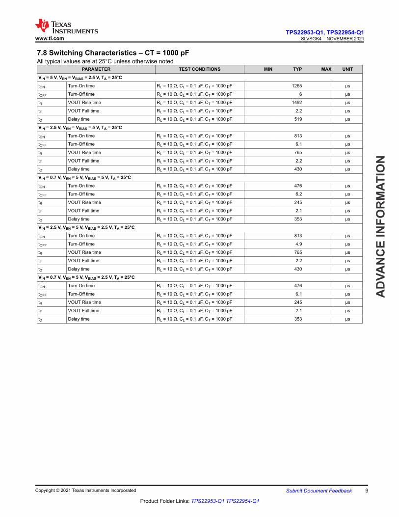
Rise time can be calculated by multiplying the input voltage (typically 10% to 90%) by the slew rate. Table 9-1 contains rise time values measured on a typical device.
Table 9-1. Rise Time
CTx (pF)RISE TIME (µs) 10%–90%, CL = 0.1 µF, VBIAS = 2.5 V to 5.7 V, RL = 10-Ω LOAD.
TYPICAL VALUES AT 25°C, 25 V X7R 10% CERAMIC CAP5 V 3.3 V 1.8 V 1.5 V 1.2 V 0.7 V
The TPS2295x-Q1 operates regardless of power-on and power-off sequencing order. The order in which voltages are applied to IN, BIAS, and EN does not damage the device as long as the voltages do not exceed the absolute maximum operating conditions. If voltage is applied to EN before IN and BIAS, the slew rate of VOUT is not controlled. Also, turning off IN or BIAS while EN is high does not damage the device.
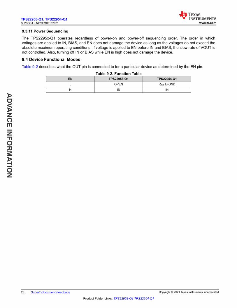
9.4 Device Functional ModesTable 9-2 describes what the OUT pin is connected to for a particular device as determined by the EN pin.
Table 9-2. Function TableEN TPS22953-Q1 TPS22954-Q1L OPEN RPD to GND
H IN IN
TPS22953-Q1, TPS22954-Q1SLVSGK4 – NOVEMBER 2021 www.ti.com
Information in the following applications sections is not part of the TI component specification, and TI does not warrant its accuracy or completeness. TI’s customers are responsible for determining suitability of components for their purposes, as well as validating and testing their design implementation to confirm system functionality.
10.1 Application InformationThis section highlights some of the design considerations when implementing this device in various applications. A PSPICE model for this device is also available on www.ti.com for further aid.
10.1.1 Input to Output Voltage Drop
The input to output voltage drop in the device is determined by the RON of the device and the load current. The RON of the device depends upon the VIN and VBIAS conditions of the device. Refer to the RON specification of the device in the Electrical Characteristics table of this data sheet. After the RON of the device is determined based upon the VIN and VBIAS voltage conditions, use Equation 5 to calculate the input to output voltage drop.
LOAD ONV I RD = ´ (5)
where
• ΔV is the voltage drop from IN to OUT• ILOAD is the load current• RON is the On-Resistance of the device for a specific VIN and VBIAS
An appropriate ILOAD must be chosen such that the IMAX specification of the device is not violated.
10.1.2 Thermal Considerations
The maximum IC junction temperature must be restricted to just under the thermal shutdown (TSD) limit of the device. Use Equation 6 to calculate the maximum allowable dissipation, PD(max) for a given output current and ambient temperature.
J(max) AD(max)
JA
T TP
-=
q (6)
where
• PD(max) is the maximum allowable power dissipation• TJ(max) is the maximum allowable junction temperature before hitting thermal shutdown (see the Electrical
Characteristics table)• TA is the ambient temperature of the device• θJA is the junction to air thermal impedance. See the thermal Information section. This parameter is highly
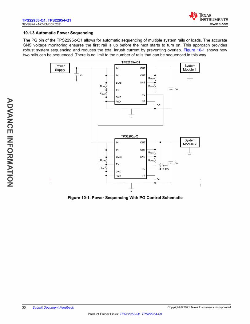
The PG pin of the TPS2295x-Q1 allows for automatic sequencing of multiple system rails or loads. The accurate SNS voltage monitoring ensures the first rail is up before the next starts to turn on. This approach provides robust system sequencing and reduces the total inrush current by preventing overlap. Figure 10-1 shows how two rails can be sequenced. There is no limit to the number of rails that can be sequenced in this way.
Figure 10-1. Power Sequencing With PG Control Schematic
TPS22953-Q1, TPS22954-Q1SLVSGK4 – NOVEMBER 2021 www.ti.com
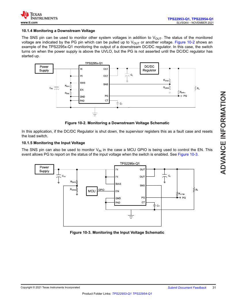
The SNS pin can be used to monitor other system voltages in addition to VOUT. The status of the monitored voltage are indicated by the PG pin which can be pulled up to VOUT or another voltage. Figure 10-2 shows an example of the TPS2295x-Q1 monitoring the output of a downstream DC/DC regulator. In this case, the switch turns on when the power supply is above the UVLO, but the PG is not asserted until the DC/DC regulator has started up.
Figure 10-2. Monitoring a Downstream Voltage Schematic
In this application, if the DC/DC Regulator is shut down, the supervisor registers this as a fault case and resets the load switch.
10.1.5 Monitoring the Input Voltage
The SNS pin can also be used to monitor VIN in the case a MCU GPIO is being used to control the EN. This event allows PG to report on the status of the input voltage when the switch is enabled. See Figure 10-3.
Figure 10-3. Monitoring the Input Voltage Schematic
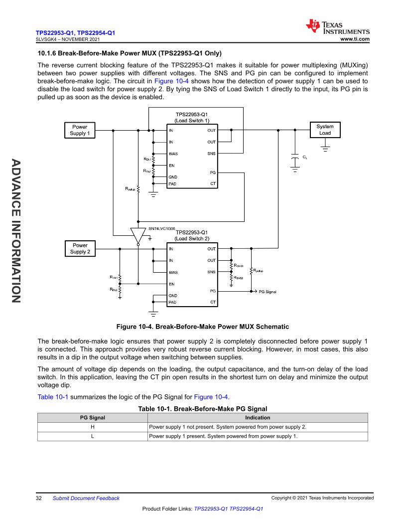
10.1.6 Break-Before-Make Power MUX (TPS22953-Q1 Only)
The reverse current blocking feature of the TPS22953-Q1 makes it suitable for power multiplexing (MUXing) between two power supplies with different voltages. The SNS and PG pin can be configured to implement break-before-make logic. The circuit in Figure 10-4 shows how the detection of power supply 1 can be used to disable the load switch for power supply 2. By tying the SNS of Load Switch 1 directly to the input, its PG pin is pulled up as soon as the device is enabled.
Figure 10-4. Break-Before-Make Power MUX Schematic
The break-before-make logic ensures that power supply 2 is completely disconnected before power supply 1 is connected. This approach provides very robust reverse current blocking. However, in most cases, this also results in a dip in the output voltage when switching between supplies.
The amount of voltage dip depends on the loading, the output capacitance, and the turn-on delay of the load switch. In this application, leaving the CT pin open results in the shortest turn on delay and minimize the output voltage dip.
Table 10-1 summarizes the logic of the PG Signal for Figure 10-4.
Table 10-1. Break-Before-Make PG SignalPG Signal Indication
H Power supply 1 not present. System powered from power supply 2.
L Power supply 1 present. System powered from power supply 1.
TPS22953-Q1, TPS22954-Q1SLVSGK4 – NOVEMBER 2021 www.ti.com
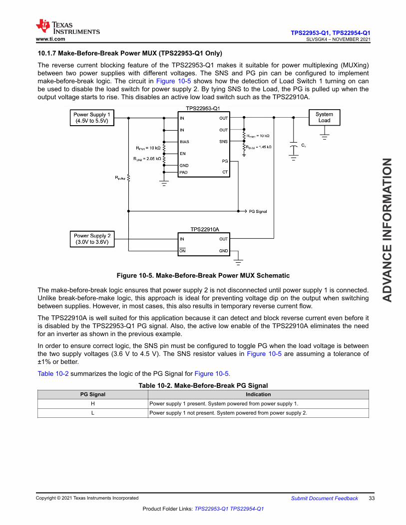
10.1.7 Make-Before-Break Power MUX (TPS22953-Q1 Only)
The reverse current blocking feature of the TPS22953-Q1 makes it suitable for power multiplexing (MUXing) between two power supplies with different voltages. The SNS and PG pin can be configured to implement make-before-break logic. The circuit in Figure 10-5 shows how the detection of Load Switch 1 turning on can be used to disable the load switch for power supply 2. By tying SNS to the Load, the PG is pulled up when the output voltage starts to rise. This disables an active low load switch such as the TPS22910A.
Figure 10-5. Make-Before-Break Power MUX Schematic
The make-before-break logic ensures that power supply 2 is not disconnected until power supply 1 is connected. Unlike break-before-make logic, this approach is ideal for preventing voltage dip on the output when switching between supplies. However, in most cases, this also results in temporary reverse current flow.
The TPS22910A is well suited for this application because it can detect and block reverse current even before it is disabled by the TPS22953-Q1 PG signal. Also, the active low enable of the TPS22910A eliminates the need for an inverter as shown in the previous example.
In order to ensure correct logic, the SNS pin must be configured to toggle PG when the load voltage is between the two supply voltages (3.6 V to 4.5 V). The SNS resistor values in Figure 10-5 are assuming a tolerance of ±1% or better.
Table 10-2 summarizes the logic of the PG Signal for Figure 10-5.
Table 10-2. Make-Before-Break PG SignalPG Signal Indication
H Power supply 1 present. System powered from power supply 1.
L Power supply 1 not present. System powered from power supply 2.
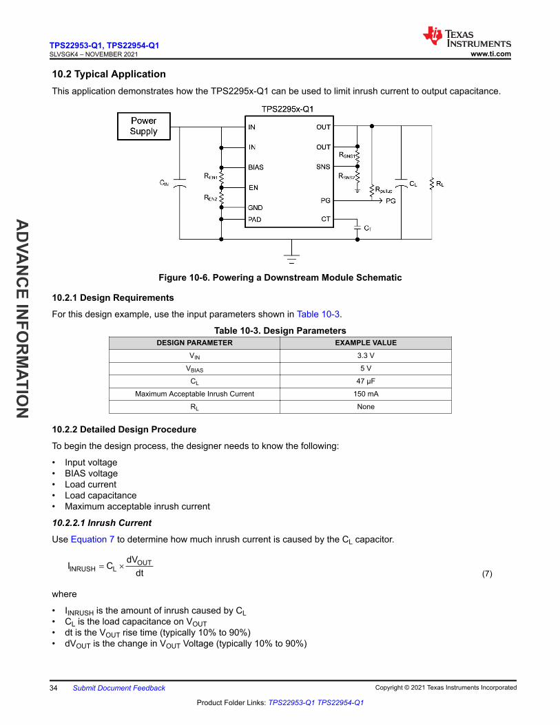
10.2 Typical ApplicationThis application demonstrates how the TPS2295x-Q1 can be used to limit inrush current to output capacitance.
Figure 10-6. Powering a Downstream Module Schematic
10.2.1 Design Requirements
For this design example, use the input parameters shown in Table 10-3.
Table 10-3. Design ParametersDESIGN PARAMETER EXAMPLE VALUE
VIN 3.3 V
VBIAS 5 V
CL 47 µF
Maximum Acceptable Inrush Current 150 mA
RL None
10.2.2 Detailed Design Procedure
To begin the design process, the designer needs to know the following:
• Input voltage• BIAS voltage• Load current• Load capacitance• Maximum acceptable inrush current
10.2.2.1 Inrush Current
Use Equation 7 to determine how much inrush current is caused by the CL capacitor.
OUTINRUSH L
dVI C
dt= ´
(7)
where
• IINRUSH is the amount of inrush caused by CL• CL is the load capacitance on VOUT• dt is the VOUT rise time (typically 10% to 90%)• dVOUT is the change in VOUT Voltage (typically 10% to 90%)
TPS22953-Q1, TPS22954-Q1SLVSGK4 – NOVEMBER 2021 www.ti.com
In this case, a Slew Rate slower than 314 μs/V is required to meet the maximum acceptable inrush requirement. Equation 4 can be used to estimate the CT capacitance (as shown in Equation 8 and Equation 9) required for this slew rate.
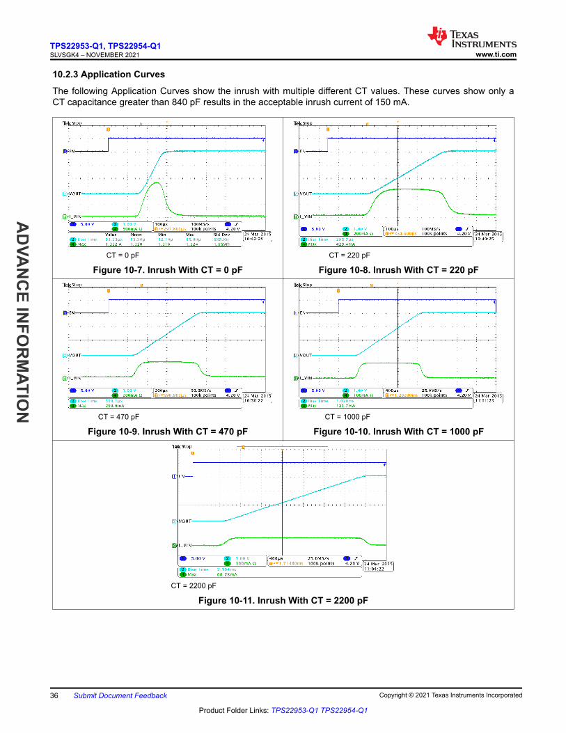
The following Application Curves show the inrush with multiple different CT values. These curves show only a CT capacitance greater than 840 pF results in the acceptable inrush current of 150 mA.
CT = 0 pF
Figure 10-7. Inrush With CT = 0 pFCT = 220 pF
Figure 10-8. Inrush With CT = 220 pF
CT = 470 pF
Figure 10-9. Inrush With CT = 470 pFCT = 1000 pF
Figure 10-10. Inrush With CT = 1000 pF
CT = 2200 pF
Figure 10-11. Inrush With CT = 2200 pF
TPS22953-Q1, TPS22954-Q1SLVSGK4 – NOVEMBER 2021 www.ti.com
11 Power Supply RecommendationsThe device is designed to operate from a VBIAS range of 2.5 V to 5.7 V and a VIN range of 0.7 V to 5.7 V. The power supply must be well regulated and placed as close to the device terminals as possible. The power supply must be able to withstand all transient and load current steps. In most situations, using an input capacitance of 1 µF is sufficient to prevent the supply voltage from dipping when the switch is turned on. In cases where the power supply is slow to respond to a large transient current or large load current step, additional bulk capacitance can be required on the input.
The requirements for larger input capacitance can be mitigated by adding additional capacitance to the CT pin. This action causes the load switch to turn on more slowly. Not only does this event reduce transient inrush current, but it also gives the power supply more time to respond to the load current step.
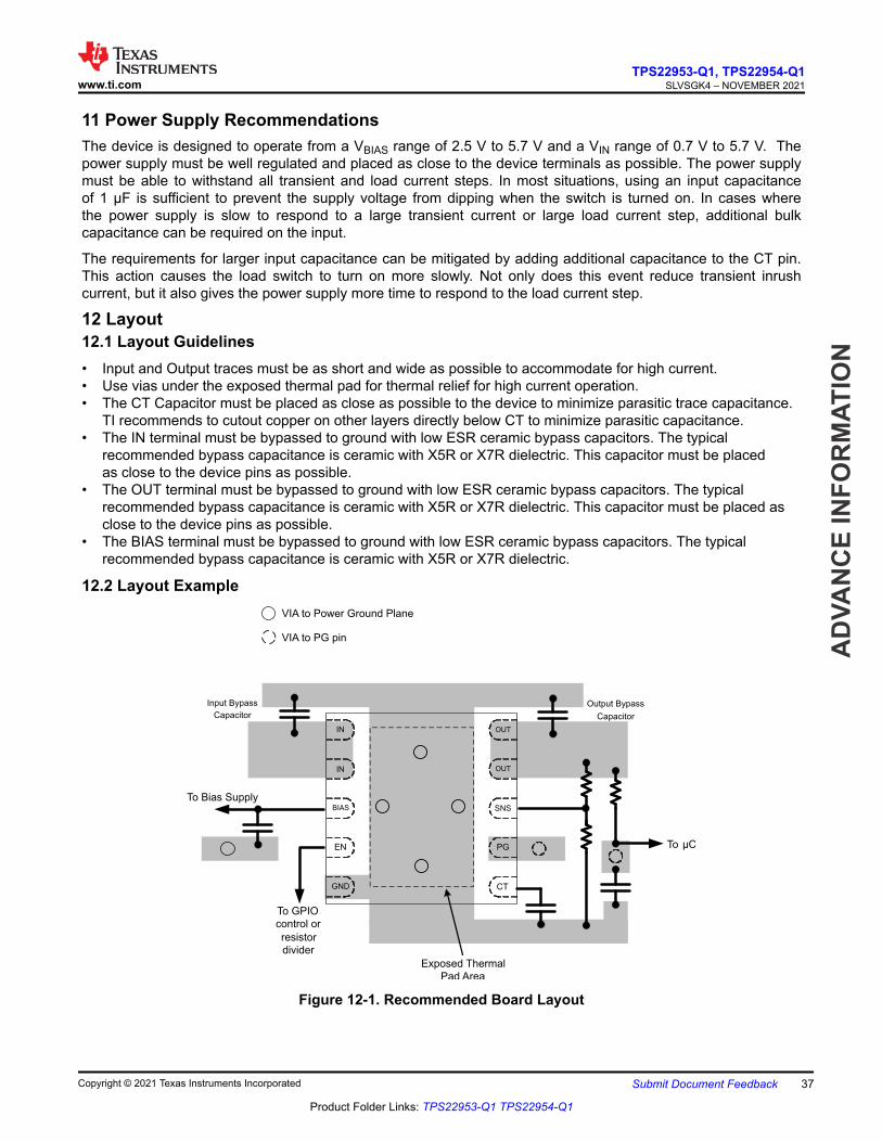
12 Layout12.1 Layout Guidelines• Input and Output traces must be as short and wide as possible to accommodate for high current.• Use vias under the exposed thermal pad for thermal relief for high current operation.• The CT Capacitor must be placed as close as possible to the device to minimize parasitic trace capacitance.
TI recommends to cutout copper on other layers directly below CT to minimize parasitic capacitance.• The IN terminal must be bypassed to ground with low ESR ceramic bypass capacitors. The typical
recommended bypass capacitance is ceramic with X5R or X7R dielectric. This capacitor must be placed as close to the device pins as possible.
• The OUT terminal must be bypassed to ground with low ESR ceramic bypass capacitors. The typical recommended bypass capacitance is ceramic with X5R or X7R dielectric. This capacitor must be placed as close to the device pins as possible.
• The BIAS terminal must be bypassed to ground with low ESR ceramic bypass capacitors. The typical recommended bypass capacitance is ceramic with X5R or X7R dielectric.
13.2 Related LinksThe table below lists quick access links. Categories include technical documents, support and community resources, tools and software, and quick access to sample or buy.
Table 13-1. Related LinksPARTS PRODUCT FOLDER SAMPLE & BUY TECHNICAL
DOCUMENTSTOOLS &
SOFTWARESUPPORT & COMMUNITY
TPS22953-Q1 Click here Click here Click here Click here Click here
TPS22954-Q1 Click here Click here Click here Click here Click here
13.3 Receiving Notification of Documentation UpdatesTo receive notification of documentation updates, navigate to the device product folder on ti.com. Click on Subscribe to updates to register and receive a weekly digest of any product information that has changed. For change details, review the revision history included in any revised document.
13.4 Support ResourcesTI E2E™ support forums are an engineer's go-to source for fast, verified answers and design help — straight from the experts. Search existing answers or ask your own question to get the quick design help you need.
Linked content is provided "AS IS" by the respective contributors. They do not constitute TI specifications and do not necessarily reflect TI's views; see TI's Terms of Use.
13.5 TrademarksTI E2E™ is a trademark of Texas Instruments.All trademarks are the property of their respective owners.13.6 Electrostatic Discharge Caution
This integrated circuit can be damaged by ESD. Texas Instruments recommends that all integrated circuits be handled with appropriate precautions. Failure to observe proper handling and installation procedures can cause damage.ESD damage can range from subtle performance degradation to complete device failure. Precision integrated circuits may be more susceptible to damage because very small parametric changes could cause the device not to meet its published specifications.
13.7 GlossaryTI Glossary This glossary lists and explains terms, acronyms, and definitions.
14 Mechanical, Packaging, and Orderable InformationThe following pages include mechanical, packaging, and orderable information. This information is the most current data available for the designated devices. This data is subject to change without notice and revision of this document. For browser-based versions of this data sheet, refer to the left-hand navigation.
TPS22953-Q1, TPS22954-Q1SLVSGK4 – NOVEMBER 2021 www.ti.com
WSON - 0.8mm max heightDQC0010APLASTIC SMALL OUTLINE - NO LEAD
PIN 1 INDEX AREA
0.08
SEATING PLANE
X0.2)(45PIN 1 ID
1
5
0.1 C A B
0.05 C
6
10
SEE OPTIONALTERMINALDETAIL
11
SYMM
SYMM
NOTES:
1. All linear dimensions are in millimeters. Any dimensions in parenthesis are for reference only. Dimensioning and tolerancingper ASME Y14.5M.
2. This drawing is subject to change without notice.3. The package thermal pad must be soldered to the printed circuit board for thermal and mechanical performance.
WSON - 0.8mm max heightDQC0010APLASTIC SMALL OUTLINE - NO LEAD
SYMM
1
5 6
10
11
SCALE: 30XLAND PATTERN EXAMPLE
NOTES: (continued)
4. This package is designed to be soldered to a thermal pad on the board. For more information, see Texas Instruments literaturenumber SLUA271 (www.ti.com/lit/slua271).
5. Vias are optional depending on application, refer to device data sheet. If any vias are implemented, refer to their locations shownon this view. It is recommended that vias under paste be filled, plugged or tented.
SOLDER MASKOPENING
METAL
SOLDER MASKDEFINED
METAL
SOLDER MASKOPENING
NON SOLDER MASK
SOLDER MASK DETAILS
DEFINED(PREFERRED)
TPS22953-Q1, TPS22954-Q1SLVSGK4 – NOVEMBER 2021 www.ti.com
WSON - 0.8mm max heightDQC0010APLASTIC SMALL OUTLINE - NO LEAD
6. Laser cutting apertures with trapezoidal walls and rounded corners may offer better paste release. IPC-7525 may have alternatedesign recommendations.
SYMM
SYMM
TYPMETAL
1
5 6
10
11
BASED ON 0.125 mm THICK STENCILSOLDER PASTE EXAMPLE
EXPOSED PAD 11:86% PRINTED SOLDER COVERAGE BY AREA UNDER PACKAGE
PTPS22953QDQCRQ1 ACTIVE WSON DQC 10 3000 TBD Call TI Call TI -40 to 125
PTPS22954QDQCRQ1 ACTIVE WSON DQC 10 3000 TBD Call TI Call TI -40 to 125
(1) The marketing status values are defined as follows:ACTIVE: Product device recommended for new designs.LIFEBUY: TI has announced that the device will be discontinued, and a lifetime-buy period is in effect.NRND: Not recommended for new designs. Device is in production to support existing customers, but TI does not recommend using this part in a new design.PREVIEW: Device has been announced but is not in production. Samples may or may not be available.OBSOLETE: TI has discontinued the production of the device.
(2) RoHS: TI defines "RoHS" to mean semiconductor products that are compliant with the current EU RoHS requirements for all 10 RoHS substances, including the requirement that RoHS substancedo not exceed 0.1% by weight in homogeneous materials. Where designed to be soldered at high temperatures, "RoHS" products are suitable for use in specified lead-free processes. TI mayreference these types of products as "Pb-Free".RoHS Exempt: TI defines "RoHS Exempt" to mean products that contain lead but are compliant with EU RoHS pursuant to a specific EU RoHS exemption.Green: TI defines "Green" to mean the content of Chlorine (Cl) and Bromine (Br) based flame retardants meet JS709B low halogen requirements of <=1000ppm threshold. Antimony trioxide basedflame retardants must also meet the <=1000ppm threshold requirement.
(3) MSL, Peak Temp. - The Moisture Sensitivity Level rating according to the JEDEC industry standard classifications, and peak solder temperature.
(4) There may be additional marking, which relates to the logo, the lot trace code information, or the environmental category on the device.
(5) Multiple Device Markings will be inside parentheses. Only one Device Marking contained in parentheses and separated by a "~" will appear on a device. If a line is indented then it is a continuationof the previous line and the two combined represent the entire Device Marking for that device.
(6) Lead finish/Ball material - Orderable Devices may have multiple material finish options. Finish options are separated by a vertical ruled line. Lead finish/Ball material values may wrap to twolines if the finish value exceeds the maximum column width.
Important Information and Disclaimer:The information provided on this page represents TI's knowledge and belief as of the date that it is provided. TI bases its knowledge and belief on informationprovided by third parties, and makes no representation or warranty as to the accuracy of such information. Efforts are underway to better integrate information from third parties. TI has taken andcontinues to take reasonable steps to provide representative and accurate information but may not have conducted destructive testing or chemical analysis on incoming materials and chemicals.TI and TI suppliers consider certain information to be proprietary, and thus CAS numbers and other limited information may not be available for release.
In no event shall TI's liability arising out of such information exceed the total purchase price of the TI part(s) at issue in this document sold by TI to Customer on an annual basis.
IMPORTANT NOTICE AND DISCLAIMERTI PROVIDES TECHNICAL AND RELIABILITY DATA (INCLUDING DATA SHEETS), DESIGN RESOURCES (INCLUDING REFERENCE DESIGNS), APPLICATION OR OTHER DESIGN ADVICE, WEB TOOLS, SAFETY INFORMATION, AND OTHER RESOURCES “AS IS” AND WITH ALL FAULTS, AND DISCLAIMS ALL WARRANTIES, EXPRESS AND IMPLIED, INCLUDING WITHOUT LIMITATION ANY IMPLIED WARRANTIES OF MERCHANTABILITY, FITNESS FOR A PARTICULAR PURPOSE OR NON-INFRINGEMENT OF THIRD PARTY INTELLECTUAL PROPERTY RIGHTS.These resources are intended for skilled developers designing with TI products. You are solely responsible for (1) selecting the appropriate TI products for your application, (2) designing, validating and testing your application, and (3) ensuring your application meets applicable standards, and any other safety, security, regulatory or other requirements.These resources are subject to change without notice. TI grants you permission to use these resources only for development of an application that uses the TI products described in the resource. Other reproduction and display of these resources is prohibited. No license is granted to any other TI intellectual property right or to any third party intellectual property right. TI disclaims responsibility for, and you will fully indemnify TI and its representatives against, any claims, damages, costs, losses, and liabilities arising out of your use of these resources.TI’s products are provided subject to TI’s Terms of Sale or other applicable terms available either on ti.com or provided in conjunction with such TI products. TI’s provision of these resources does not expand or otherwise alter TI’s applicable warranties or warranty disclaimers for TI products.TI objects to and rejects any additional or different terms you may have proposed. IMPORTANT NOTICE