3-V TO 5.5-V MULTICHANNEL RS-232 LINE DRIVER/RECEIVERWITH ±15-kV IEC ESD PROTECTION
• Qualified for Automotive Applications• ESD Protection for RS-232 Bus Pins
– ±15-kV Human Body Model (HBM)– ±8 kV (IEC61000-4-2, Contact Discharge)– ±15 kV (IEC61000-4-2, Air-Gap Discharge)
• Meets or Exceeds the Requirements ofTIA/EIA-232-F and ITU v.28 Standards
• Operates With 3-V to 5.5-V VCC Supply• Operates up to 250 kbit/s• Two Drivers and Two Receivers• Low Supply Current: 300 µA (Typ)• External Capacitors: 4 × 0.1 µF• Accepts 5-V Logic Input With 3.3-V Supply• Pin Compatible to Alternative High-Speed
Device (1 Mbit/s): TRSF3232E
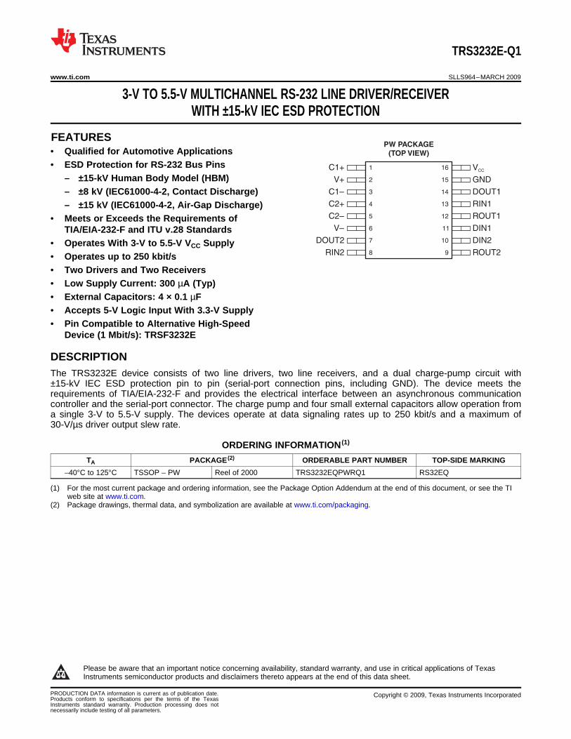
The TRS3232E device consists of two line drivers, two line receivers, and a dual charge-pump circuit with±15-kV IEC ESD protection pin to pin (serial-port connection pins, including GND). The device meets therequirements of TIA/EIA-232-F and provides the electrical interface between an asynchronous communicationcontroller and the serial-port connector. The charge pump and four small external capacitors allow operation froma single 3-V to 5.5-V supply. The devices operate at data signaling rates up to 250 kbit/s and a maximum of30-V/µs driver output slew rate.
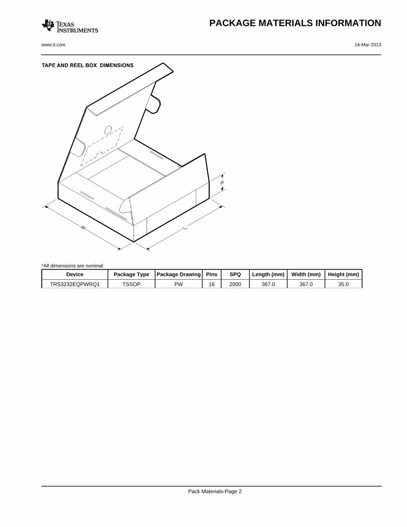
ORDERING INFORMATION (1)
TA PACKAGE (2) ORDERABLE PART NUMBER TOP-SIDE MARKING–40°C to 125°C TSSOP – PW Reel of 2000 TRS3232EQPWRQ1 RS32EQ
(1) For the most current package and ordering information, see the Package Option Addendum at the end of this document, or see the TIweb site at www.ti.com.
(2) Package drawings, thermal data, and symbolization are available at www.ti.com/packaging.
1
Please be aware that an important notice concerning availability, standard warranty, and use in critical applications of TexasInstruments semiconductor products and disclaimers thereto appears at the end of this data sheet.
over operating free-air temperature range (unless otherwise noted)
VCC Supply voltage range (2) –0.3 V to 6 VV+ Positive output supply voltage range (2) –0.3 V to 7 VV– Negative output supply voltage range (2) 0.3 V to –7 VV+ – V– Supply voltage difference (2) 13 V
Drivers –0.3 V to 6 VVI Input voltage range
Receivers –25 V to 25 VDrivers –13.2 V to 13.2 V
VO Output voltage rangeReceivers –0.3 V to VCC + 0.3 V
θJA Package thermal impedance (3) (4) 108°C/WTJ Operating virtual-junction temperature 150°CTstg Storage temperature range –65°C to 150°C
(1) Stresses beyond those listed under "absolute maximum ratings" may cause permanent damage to the device. These are stress ratingsonly, and functional operation of the device at these or any other conditions beyond those indicated under "recommended operatingconditions" is not implied. Exposure to absolute-maximum-rated conditions for extended periods may affect device reliability.
(2) All voltages are with respect to network GND.(3) Maximum power dissipation is a function of TJ(max), θJA, and TA. The maximum allowable power dissipation at any allowable ambient
temperature is PD = (TJ(max) – TA)/θJA. Operating at the absolute maximum TJ of 150°C can affect reliability.(4) The package thermal impedance is calculated in accordance with JESD 51-7.
See Figure 4
MIN NOM MAX UNITVCC = 3.3 V 3 3.3 3.6
VCC Supply voltage VVCC = 5 V 4.5 5 5.5VCC = 3.3 V 2 5.5
VIH Driver high-level input voltage, DIN VVCC = 5 V 2.4 5.5
VIL Driver low-level input voltage, DIN 0 0.8 VVI Receiver input voltage –25 25 VTA Operating free-air temperature –40 125 °C
(1) Test conditions are C1–C4 = 0.1 µF at VCC = 3.3 V ± 0.3 V; C1 = 0.047 µF, C2–C4 = 0.33 µF at VCC = 5 V ± 0.5 V.
over recommended ranges of supply voltage and operating free-air temperature (unless otherwise noted) (see Figure 4)
PARAMETER TEST CONDITIONS MIN TYP (2) MAX UNITICC Supply current No load, VCC = 3.3 V or 5 V 0.3 1 mA
(1) Test conditions are C1–C4 = 0.1 µF at VCC = 3.3 V ± 0.3 V; C1 = 0.047 µF, C2–C4 = 0.33 µF at VCC = 5 V ± 0.5 V.(2) All typical values are at VCC = 3.3 V or VCC = 5 V, and TA = 25°C.
over recommended ranges of supply voltage and operating free-air temperature (unless otherwise noted) (see Figure 4)
PARAMETER TEST CONDITIONS MIN TYP (2) MAX UNITVOH High-level output voltage DOUT at RL = 3 kΩ to GND, DIN = GND 5 5.4 VVOL Low-level output voltage DOUT at RL = 3 kΩ to GND, DIN = VCC –5 –5.4 VIIH High-level input current VI = VCC ±0.01 ±1 µAIIL Low-level input current VI at GND ±0.01 ±1 µA
VCC = 3.6 V, VO = 0 V ±35 ±60IOS
(3) Short-circuit output current mAVCC = 5.5 V, VO = 0 V ±35 ±60
ro Output resistance VCC, V+, and V– = 0 V, VO = ±2 V 300 10M Ω
(1) Test conditions are C1–C4 = 0.1 µF at VCC = 3.3 V ± 0.3 V; C1 = 0.047 µF, C2–C4 = 0.33 µF at VCC = 5 V ± 0.5 V.(2) All typical values are at VCC = 3.3 V or VCC = 5 V, and TA = 25°C.(3) Short-circuit durations should be controlled to prevent exceeding the device absolute power dissipation ratings, and not more than one
output should be shorted at a time.
over recommended ranges of supply voltage and operating free-air temperature (unless otherwise noted) (see Figure 4)
PARAMETER TEST CONDITIONS MIN TYP (2) MAX UNITCL = 1000 pF, RL = 3 kΩ, One DOUT switching,Maximum data rate 150 250 kbit/sSee Figure 1CL = 150 pF to 2500 pF, RL = 3 kΩ to 7 kΩ,tsk(p) Pulse skew (3) 300 nsSee Figure 2
CL = 150 pF to 1000 pF 6 30Slew rate, transition region RL = 3 kΩ to 7 kΩ,SR(tr) V/µs(see Figure 1) VCC = 3.3 V CL = 150 pF to 2500 pF 4 30
(1) Test conditions are C1–C4 = 0.1 µF at VCC = 3.3 V ± 0.3 V; C1 = 0.047 µF, C2–C4 = 0.33 µF at VCC = 5 V ± 0.5 V.(2) All typical values are at VCC = 3.3 V or VCC = 5 V, and TA = 25°C.(3) Pulse skew is defined as |tPLH – tPHL| of each channel of the same device.
over recommended ranges of supply voltage and operating free-air temperature (unless otherwise noted) (see Figure 4)
PARAMETER TEST CONDITIONS MIN TYP (2) MAX UNITVOH High-level output voltage IOH = –1 mA VCC – 0.6 VCC – 0.1 VVOL Low-level output voltage IOL = 1.6 mA 0.4 V
VCC = 3.3 V 1.5 2.4VIT+ Positive-going input threshold voltage V
VCC = 5 V 1.8 2.4VCC = 3.3 V 0.6 1.2
VIT– Negative-going input threshold voltage VVCC = 5 V 0.8 1.5
Vhys Input hysteresis (VIT+ – VIT–) 0.3 Vri Input resistance VI = ±3 V to ±25 V 3 5 7 kΩ
(1) Test conditions are C1–C4 = 0.1 µF at VCC = 3.3 V ± 0.3 V; C1 = 0.047 µF, C2–C4 = 0.33 µF at VCC = 5 V ± 0.5 V.(2) All typical values are at VCC = 3.3 V or VCC = 5 V, and TA = 25°C.
over recommended ranges of supply voltage and operating free-air temperature (unless otherwise noted) (see Figure 3)
PARAMETER TEST CONDITIONS TYP (2) UNITtPLH Propagation delay time, low- to high-level output 300 ns
CL = 150 pFtPHL Propagation delay time, high- to low-level output 300 nstsk(p) Pulse skew (3) 300 ns
(1) Test conditions are C1–C4 = 0.1 µF at VCC = 3.3 V ± 0.3 V; C1 = 0.047 µF, C2–C4 = 0.33 µF at VCC = 5 V ± 0.5 V.(2) All typical values are at VCC = 3.3 V or VCC = 5 V, and TA = 25°C.(3) Pulse skew is defined as |tPLH – tPHL| of each channel of the same device.
NOTES: A. CL includes probe and jig capacitance.B. The pulse generator has the following characteristics: PRR = 250 kbit/s, ZO = 50 Ω, 50% duty cycle, tr ≤ 10 ns, tf ≤ 10 ns.
1.5 V 1.5 V
3 V−3 V
3 V
−3 V
TEST CIRCUIT VOLTAGE WAVEFORMS
0 V
3 V
Output
Input
VOL
VOH
tPLHtPHL
50% 50%
NOTES: A. CL includes probe and jig capacitance.B. The pulse generator has the following characteristics: PRR = 250 kbit/s, ZO = 50 Ω, 50% duty cycle, tr ≤ 10 ns, tf ≤ 10 ns.
1.5 V 1.5 V
50 ΩGenerator
(see Note B)RL
RS-232Output
CL
(see Note A)
TEST CIRCUIT VOLTAGE WAVEFORMS
50 Ω
50%50%
−3 V
3 V1.5 V1.5 V
Output
Input
VOL
VOH
tPHL
Generator(see Note B) tPLH
Output
CL
(see Note A)
NOTES: A. CL includes probe and jig capacitance.B. The pulse generator has the following characteristics: ZO = 50 Ω, 50% duty cycle, tr ≤ 10 ns, tf ≤ 10 ns.
TRS3232EQPWRQ1 ACTIVE TSSOP PW 16 2000 Green (RoHS& no Sb/Br)
CU NIPDAU Level-1-260C-UNLIM -40 to 125 RS32EQ
(1) The marketing status values are defined as follows:ACTIVE: Product device recommended for new designs.LIFEBUY: TI has announced that the device will be discontinued, and a lifetime-buy period is in effect.NRND: Not recommended for new designs. Device is in production to support existing customers, but TI does not recommend using this part in a new design.PREVIEW: Device has been announced but is not in production. Samples may or may not be available.OBSOLETE: TI has discontinued the production of the device.
(2) Eco Plan - The planned eco-friendly classification: Pb-Free (RoHS), Pb-Free (RoHS Exempt), or Green (RoHS & no Sb/Br) - please check http://www.ti.com/productcontent for the latest availabilityinformation and additional product content details.TBD: The Pb-Free/Green conversion plan has not been defined.Pb-Free (RoHS): TI's terms "Lead-Free" or "Pb-Free" mean semiconductor products that are compatible with the current RoHS requirements for all 6 substances, including the requirement thatlead not exceed 0.1% by weight in homogeneous materials. Where designed to be soldered at high temperatures, TI Pb-Free products are suitable for use in specified lead-free processes.Pb-Free (RoHS Exempt): This component has a RoHS exemption for either 1) lead-based flip-chip solder bumps used between the die and package, or 2) lead-based die adhesive used betweenthe die and leadframe. The component is otherwise considered Pb-Free (RoHS compatible) as defined above.Green (RoHS & no Sb/Br): TI defines "Green" to mean Pb-Free (RoHS compatible), and free of Bromine (Br) and Antimony (Sb) based flame retardants (Br or Sb do not exceed 0.1% by weightin homogeneous material)
(3) MSL, Peak Temp. -- The Moisture Sensitivity Level rating according to the JEDEC industry standard classifications, and peak solder temperature.
(4) Multiple Top-Side Markings will be inside parentheses. Only one Top-Side Marking contained in parentheses and separated by a "~" will appear on a device. If a line is indented then it is acontinuation of the previous line and the two combined represent the entire Top-Side Marking for that device.
Important Information and Disclaimer:The information provided on this page represents TI's knowledge and belief as of the date that it is provided. TI bases its knowledge and belief on informationprovided by third parties, and makes no representation or warranty as to the accuracy of such information. Efforts are underway to better integrate information from third parties. TI has taken andcontinues to take reasonable steps to provide representative and accurate information but may not have conducted destructive testing or chemical analysis on incoming materials and chemicals.TI and TI suppliers consider certain information to be proprietary, and thus CAS numbers and other limited information may not be available for release.
In no event shall TI's liability arising out of such information exceed the total purchase price of the TI part(s) at issue in this document sold by TI to Customer on an annual basis.
Texas Instruments Incorporated and its subsidiaries (TI) reserve the right to make corrections, enhancements, improvements and otherchanges to its semiconductor products and services per JESD46, latest issue, and to discontinue any product or service per JESD48, latestissue. Buyers should obtain the latest relevant information before placing orders and should verify that such information is current andcomplete. All semiconductor products (also referred to herein as “components”) are sold subject to TI’s terms and conditions of salesupplied at the time of order acknowledgment.TI warrants performance of its components to the specifications applicable at the time of sale, in accordance with the warranty in TI’s termsand conditions of sale of semiconductor products. Testing and other quality control techniques are used to the extent TI deems necessaryto support this warranty. Except where mandated by applicable law, testing of all parameters of each component is not necessarilyperformed.TI assumes no liability for applications assistance or the design of Buyers’ products. Buyers are responsible for their products andapplications using TI components. To minimize the risks associated with Buyers’ products and applications, Buyers should provideadequate design and operating safeguards.TI does not warrant or represent that any license, either express or implied, is granted under any patent right, copyright, mask work right, orother intellectual property right relating to any combination, machine, or process in which TI components or services are used. Informationpublished by TI regarding third-party products or services does not constitute a license to use such products or services or a warranty orendorsement thereof. Use of such information may require a license from a third party under the patents or other intellectual property of thethird party, or a license from TI under the patents or other intellectual property of TI.Reproduction of significant portions of TI information in TI data books or data sheets is permissible only if reproduction is without alterationand is accompanied by all associated warranties, conditions, limitations, and notices. TI is not responsible or liable for such altereddocumentation. Information of third parties may be subject to additional restrictions.Resale of TI components or services with statements different from or beyond the parameters stated by TI for that component or servicevoids all express and any implied warranties for the associated TI component or service and is an unfair and deceptive business practice.TI is not responsible or liable for any such statements.Buyer acknowledges and agrees that it is solely responsible for compliance with all legal, regulatory and safety-related requirementsconcerning its products, and any use of TI components in its applications, notwithstanding any applications-related information or supportthat may be provided by TI. Buyer represents and agrees that it has all the necessary expertise to create and implement safeguards whichanticipate dangerous consequences of failures, monitor failures and their consequences, lessen the likelihood of failures that might causeharm and take appropriate remedial actions. Buyer will fully indemnify TI and its representatives against any damages arising out of the useof any TI components in safety-critical applications.In some cases, TI components may be promoted specifically to facilitate safety-related applications. With such components, TI’s goal is tohelp enable customers to design and create their own end-product solutions that meet applicable functional safety standards andrequirements. Nonetheless, such components are subject to these terms.No TI components are authorized for use in FDA Class III (or similar life-critical medical equipment) unless authorized officers of the partieshave executed a special agreement specifically governing such use.Only those TI components which TI has specifically designated as military grade or “enhanced plastic” are designed and intended for use inmilitary/aerospace applications or environments. Buyer acknowledges and agrees that any military or aerospace use of TI componentswhich have not been so designated is solely at the Buyer's risk, and that Buyer is solely responsible for compliance with all legal andregulatory requirements in connection with such use.TI has specifically designated certain components as meeting ISO/TS16949 requirements, mainly for automotive use. In any case of use ofnon-designated products, TI will not be responsible for any failure to meet ISO/TS16949.
Products ApplicationsAudio www.ti.com/audio Automotive and Transportation www.ti.com/automotiveAmplifiers amplifier.ti.com Communications and Telecom www.ti.com/communicationsData Converters dataconverter.ti.com Computers and Peripherals www.ti.com/computersDLP® Products www.dlp.com Consumer Electronics www.ti.com/consumer-appsDSP dsp.ti.com Energy and Lighting www.ti.com/energyClocks and Timers www.ti.com/clocks Industrial www.ti.com/industrialInterface interface.ti.com Medical www.ti.com/medicalLogic logic.ti.com Security www.ti.com/securityPower Mgmt power.ti.com Space, Avionics and Defense www.ti.com/space-avionics-defenseMicrocontrollers microcontroller.ti.com Video and Imaging www.ti.com/videoRFID www.ti-rfid.comOMAP Applications Processors www.ti.com/omap TI E2E Community e2e.ti.comWireless Connectivity www.ti.com/wirelessconnectivity


![Multichannel texture analysis using localized spatial ...€¦ · ful for analyzing textured images containing highly spe- cific frequency or orientation characteristics [4]-[6].](https://static.documents.pub/doc/80x56/5f6ac4132125bf5a5403855a/multichannel-texture-analysis-using-localized-spatial-ful-for-analyzing-textured.jpg)


