105
32bit TX System RISC TX19A Family TMP19A43FD/FZXBG Rev2.0 2007.Apr.9

32bit TX System RISC
TX19A Family
TMP19A43FD/FZXBG
Rev2.0 2007.Apr.9

TMP19A43
TMP19A43 (rev2.0) 1-1 Overview and Features
32-bit RISC Microprocessor - TX19 Family
TMP19A43FZXBG, FDXBG
1. Overview and Features
The TX19 family is a high-performance 32-bit RISC processor series that TOSHIBA originally developed by
integrating the MIPS16TMASE (Application Specific Extension), which is an extended instruction set of high code
efficiency.
TMP19A43 is a 32-bit RISC microprocessor with a TX19A processor core and various peripheral functions
integrated into one package. It can operate at low voltage with low power consumption.
Features of TMP19A43 are as follows:
RESTRICTIONS ON PRODUCT USE 070122EBP
• The information contained herein is subject to change without notice. 021023_D • TOSHIBA is continually working to improve the quality and reliability of its products. Nevertheless, semiconductor
devices in general can malfunction or fail due to their inherent electrical sensitivity and vulnerability to physical stress. It is the responsibility of the buyer, when utilizing TOSHIBA products, to comply with the standards of safety in makinga safe design for the entire system, and to avoid situations in which a malfunction or failure of such TOSHIBA products could cause loss of human life, bodily injury or damage to property. In developing your designs, please ensure that TOSHIBA products are used within specified operating ranges as set forth in the most recent TOSHIBA products specifications. Also, please keep in mind the precautions and conditions set forth in the “Handling Guide for Semiconductor Devices,” or “TOSHIBA Semiconductor Reliability Handbook” etc. 021023_A
• The TOSHIBA products listed in this document are intended for usage in general electronics applications (computer, personal equipment, office equipment, measuring equipment, industrial robotics, domestic appliances, etc.). These TOSHIBA products are neither intended nor warranted for usage in equipment that requires extraordinarily high quality and/or reliability or a malfunction or failure of which may cause loss of human life or bodily injury (“Unintended Usage”). Unintended Usage include atomic energy control instruments, airplane or spaceship instruments, transportation instruments, traffic signal instruments, combustion control instruments, medical instruments, all types of safety devices, etc. Unintended Usage of TOSHIBA products listed in this document shall be made at the customer’s own risk. 021023_B
• The products described in this document shall not be used or embedded to any downstream products of which manufacture, use and/or sale are prohibited under any applicable laws and regulations. 060106_Q
• The information contained herein is presented only as a guide for the applications of our products. No responsibility is assumed by TOSHIBA for any infringements of patents or other rights of the third parties which may result from its use. No license is granted by implication or otherwise under any patents or other rights of TOSHIBA or the third parties. 070122_C
• The products described in this document are subject to foreign exchange and foreign trade control laws. 060925_E • For a discussion of how the reliability of microcontrollers can be predicted, please refer to Section 1.3 of the chapter
entitled Quality and Reliability Assurance/Handling Precautions. 030619_S

TMP19A43
TMP19A43 (rev2.0) 1-2 Overview and Features
(1) TX19A processor core
1) Improved code efficiency and operating performance have been realized through the use of two ISA
(Instruction Set Architecture) modes - 16- and 32-bit ISA modes.
• The 16-bit ISA mode instructions are compatible with the MIPS16TMASE instructions of superior
code efficiency at the object level.
• The 32-bit ISA mode instructions are compatible with the TX39 instructions of superior operating
performance at the object level.
2) Both high performance and low power dissipation have been achieved.
High performance
• Almost all instructions can be executed with one clock.
• High performance is possible via a three-operand operation instruction.
• 5-stage pipeline
• Built-in high-speed memory
• DSP function: A 32-bit multiplication and accumulation operation can be executed with one clock.
Low power dissipation
• Optimized design using a low power dissipation library
• Standby function that stops the operation of the processor core
3) High-speed interrupt response suitable for real-time control
• Independency of the entry address
• Automatic generation of factor-specific vector addresses
• Automatic update of interrupt mask levels
(2) Internal program memory and data memory
Product name Built-in ROM Built-in RAM
TMP19A43CZXBG 384Kbyte 20Kbyte
TMP19A43CDXBG * 512Kbyte 24Kbyte
TMP19A43FZXBG * 384Kbyte (Flash) 20Kbyte
TMP19A43FDXBG 512Kbyte (Flash) 24Kbyte
The product indicated by an asterisk * is under development.
• ROM correction function: 1 word × 8 blocks, 8 words × 4 blocks
(3) External memory expansion
• Expandable to 16 megabytes (for both programs and data)
• External data bus: Separate bus/multiplexed bus : Coexistence of 8- and 16-bit widths is possible. Chip select/wait controller : 4 channels
(4) DMA controller : 8 channels (2 interrupt factors)
• Activated by an interrupt or software
• Data to be transferred to internal memory, internal I/O, external memory, and external I/O
(5) 16-bit timer : 16 channels
• 16-bit interval timer mode
• 16-bit event counter mode
• 16-bit PPG output (every 4 channels, synchronous outputs are possible)
• Input capture function
• 2-phase pulse input counter function (4 channels assigned to perform this function): Multiplication-by-4 mode
TMP19A43
TMP19A43 (rev2.0) 1-3 Overview and Features
(6) 32-bit timer
• 32-bit input capture register : 4 channels
• 32-bit compare register : 8 channels
• 32-bit time base timer : 1 channel
(7) Clock timer : 1 channel
(8) General-purpose serial interface : 3 channels
• Selectable between the UART mode and the synchronization mode
(9) High-speed serial interface : 3 channels
• Selectable between the UART mode and the high-speed synchronization mode (maximum speed: 10 Mbps in the high-speed synchronization mode @40MHz)
(10) Serial bus interface : 1 channel
• Selectable between the I2C bus mode and the clock synchronization mode
(11) 10-bit A/D converter (with S/H) : 16 channels
• Start by an external trigger, and the internal timer activated by a trigger
• Fixed channel/scan mode
• Single/repeat mode
• High-priority conversion mode
• Timer monitor function
• Conversion time 1.15 µsec(@ 40MHz)
(12) 8-bit D/A converter : 2 channels
(13) Watchdog timer : 1 channel
(14) Interrupt function
• CPU: 2 factors ...................software interrupt instruction
• Internal: 46 factors.............The order of precedence can be set over 7 levels
(except the watchdog timer interrupt).
• External: 48 factors ..........The order of precedence can be set over 7 levels.
Because 32 factors are associated with KWUP, the number of interrupt
factors is one.
(15) Input and output ports ...............143 terminals
(16) Standby function
• Three standby modes (IDLE, SLEEP, STOP)
(17) Clock generator
• Built-in PLL (multiplication by 4)
• Clock gear function: The high-speed clock can be divided into 3/4, 1/2, 1/4 or 1/8.
• Sub-clock: SLOW and SLEEP modes (32.768 kHz)
(18) Endian: Bi-endian (big-endian/little-endian)
(19) Maximum operating frequency
• 40 MHz (PLL multiplication)
(20) Operating voltage range
• Core: 1.35 V to 1.65 V
• I/O and ADC: 2.7 V to 3.6 V
• DAC: 2.3 V to 2.7 V
(21) Package
P-FBGA193 (12 mm × 12 mm, 0.65 mm pitch)

TMP19A43
TMP19A43 (rev2.0) 1-4 Overview and Features
Fig. 1-1 TMP19A43 Block Diagram
TX19 Processor Core
TX19A CPU
MAC EJTAG
512K/384byteFlash
24K/20KbyteRAM
ROM correction
DMAC (8ch)
Clock generator (CG)
INTC External bus interface
I/O bus interface
16-bit TMRB 0 to 15 (16ch)
32-bit TMRC TBT (1ch)
32-bit TMRC Input Capture 0 to 3 (4ch)
32-bit TMRC Compare
0 to 7 (8ch)
10-bit ADC (16ch) SIO/UART 0 to 2 (3ch)
I2C/SIO (1ch)
PORT0to
PORT6 (also function as external bus I/F)
WDT KWUP (32ch)
PORT7 to
PORT8 (also function to
receive ADC inputs)
PORT9to
PORTH (also function as functional pins)
Clock timer (1ch)
8-bit DAC (2ch)
HSIO/UART 0 to 2 (3ch)
TMP19A43
TMP19A43 (rev2.0) 2-1 Pin Layout and Pin Functions
2. Pin Layout and Pin Functions
This section shows the pin layout of TMP19A43 and describes the names and functions of input and output pins.
2.1 Pin Layout (Top view)
Fig. 2-1 Pin Layout Diagram (P-FBGA193) shows the pin layout of TMP19A43.
A1 A2 A3 A4 A5 A6 A7 A8 A9 A10 A11 A12 A13 A14 A15 A16 A17
B1 B2 B3 B4 B5 B6 B7 B8 B9 B10 B11 B12 B13 B14 B15 B16 B17
C1 C2 C16 C17
D1 D2 D4 D5 D6 D7 D8 D9 D10 D11 D12 D13 D14 D16 D17
E1 E2 E4 E5 E6 E7 E8 E9 E10 E11 E12 E13 E14 E16 E17
F1 F2 F4 F5 F6 F13 F14 F16 F17
G1 G2 G4 G5 G13 G14 G16 G17
H1 H2 H4 H5 H13 H14 H16 H17
J1 J2 J4 J5 J13 J14 J16 J17
K1 K2 K4 K5 K13 K14 K16 K17
L1 L2 L4 L5 L13 L14 L16 L17
M1 M2 M4 M5 M13 M14 M16 M17
N1 N2 N4 N5 N6 N7 N8 N9 N10 N11 N12 N13 N14 N16 N17
P1 P2 P4 P5 P6 P7 P8 P9 P10 P11 P12 P13 P14 P16 P17
R1 R2 R16 R17
T1 T2 T3 T4 T5 T6 T7 T8 T9 T10 T11 T12 T13 T14 T15 T16 T17
U1 U2 U3 U4 U5 U6 U7 U8 U9 U10 U11 U12 U13 U14 U15 U16 U17
Fig. 2-1 Pin Layout Diagram (P-FBGA193)

TMP19A43
TMP19A43 (rev2.0) 2-2 Pin Layout and Pin Functions
2.2 Pin Numbers and Names
Table 2-1 shows the pin numbers and names of TMP19A43.
Table 2-1 Pin numbers and names
Pin No.
Pin Name Pin No.
Pin Name Pin No.
Pin Name Pin No.
Pin Name Pin No.
Pin Name
A1 DVSS D2 PF3/KEY19/DACK4 G2 P95/SCLK2/CTS2 M1 PB5/HTXD1 R2 P33/WAIT/RDY
A2 P81/AN9/KEY05 D4 P71/AN1 G4 P94/RXD2 M2 PB4/HSCLK0/HCTS0 R16 P45/BUSMD
A3 P83/AN11/KEY07 D5 P73/AN3 G5 P93/TXD2 M4 PB3/HRXD0 R17 P46/ENDIAN
A4 P85/AN13/INT7 D6 P74/AN4/KEY00 G13 PH1/TPC1/TPD1 M5 TEST4 T1 P37/ALE/TC3IN
A5 P87/AN15/INT9 D7 P76/AN6/KEY02 G14 PH7/TPC7/TPD7 M13 FVCC3 T2 P34/BUSRQ/TBEOUT
A6 DA0 D8 PD5/TBDOUT G16 PCST4 M14 PG3/TPD3 T3 P30/RD
A7 CVREF0 D9 PD3/TBBOUT G17 DCLK M16 PG4/TPD4 T4 P02/D2/AD2
A8 DA1 D10 PD0/HTXD2 H1 PC1/TCOUT0 M17 PG5/TPD2 T5 P06/D6/AD6
A9 CVREF1 D11 PE0/KEY8 H2 PC0/TBTIN/KEY30 N1 PB7/HSCLK1/HCTS1 T6 P12/D10/AD10/A10
A10 PD2/HSCLK2/HCTS2 D12 PE3/KEY11 H4 P97/TBAOUT N2 PB6/HRXD1 T7 P16/D14/AD14/A14
A11 PE2/KEY10 D13 PA2/INT2/TB7IN0 H5 DVCC3 N4 P00/D0/AD0 T8 P21/A17/A1/TB0IN1
A12 PE5/KEY13 D14 PH4/TPC4/TPD4 H13 PH2/TPC2/TPD2 N5 P04/D4/AD4 T9 P24/A20/A4/TB4IN0
A13 PE7/KEY15 D16 PA3/INT3/TB7IN1 H14 TRST N6 P10/D8/AD8/A8 T10 P26/A22/A6/TB5IN0
A14 X1 D17 XT1 H16 TMS N7 P14/D12/AD12/A12 T11 P52/A2/INTE
A15 X2 E1 PF6/KEY22/TCOUT6 H17 EJE N8 FVCC3 T12 P56/A6/TB2OUT/KEY28
A16 CVCCH E2 PF5/KEY21/TCOUT5 J1 PC4/TCOUT3 N9 DVSS T13 P62/A10/SCLK0/CTS0
A17 CVSS E4 P70/AN0 J2 PC3/TCOUT2 N10 DVCC15 T14 P66/A14/TB4OUT
B1 PF0/KEY16/DREQ0 E5 P72/AN2 J4 PC2/TCOUT1 N11 P50/A0/INTC T15 P40/CS0/KEY24
B2 P80/AN8/KEY04 E6 VREFH J5 DVCC15 N12 P54/A4/TB0OUT T16 P42/CS2/KEY26
B3 P82/AN10/KEY06 E7 AVSS J13 PH3/TPC3/TPD3 N13 P60/A8/TXD0 T17 P44/SCOUT
B4 P84/AN12/INT6 E8 DAVCC J14 DINT N14 P64/A12/RXD1/INTB U1 TEST2
B5 P86/AN14/INT8 E9 DAVREF J16 TDO N16 PG6/TPD6 U2 P35/BUSAK/TC1IN
B6 P75/AN5/KEY01 E10 DAGND J17 DVSS N17 PG7/TPD7 U3 P31/WR
B7 P77/AN7/KEY03 E11 DVCC3 K1 PC7/SCK P1 BOOT U4 P03/D3/AD3
B8 PD6/KEY31/AFTRG E12 PA0/INT0/TB6IN0 K2 PC6/SI/SCL P2 P32/HWR/TC0IN U5 P07/D7/AD7
B9 PD4/TBCOUT E13 PA1/INT1/TB6IN1 K4 PC5/SO/SDA P4 P01/D1/AD1 U6 P13/D11/AD11/A11
B10 PD1/HRXD2 E14 PH5/TPC5/TPD5 K5 DVSS P5 P05/D5/AD5 U7 P17/D15/AD15/A15
B11 PE1/KEY09 E16 PCST0 K13 DVCC15 P6 P11/D9/AD9/A9 U8 P22/A18/A2/TB1IN0
B12 PE4/KEY12 E17 PCST1 K14 TOVR/TSTA P7 P15/D13/AD13/A13 U9 P25/A21/A5/TB4IN1
B13 PE6/KEY14 F1 PF7/KEY23/TCOUT7 K16 TDI P8 P20/A16/A0/TB0IN0 U10 P27/A23/A7/TB5IN1
B14 PA5/INT5/TB8IN1 F2 P92/TB8OUT K17 TCK P9 P23/A19/A3/TB1IN1 U11 P53/A3/INTF
B15 PA6/ TB2IN0 F4 P91/TB7OUT L1 PB2/HTXD0 P10 TEST0 U12 P57/A7/TB3OUT/KEY29
B16 PA7/TB2IN1 F5 P90/TB6OUT L2 PB1/TB3IN1 P11 P51/A1/INTD U13 P63/A11/TXD1
B17 CVCCL F6 AVCC3 L4 PB0/TB3IN0 P12 P55/A5/TB1OUT U14 P67/A15/TB5OUT
C1 PF2/KEY18/DREQ4 F13 PH0/TPC0/TPD0 L5 TEST1 P13 P61/A9/RXD0/INTA U15 P41/CS1/KEY25
C2 PF1/KEY17/DACK0 F14 PH6/TPC6/TPD6 L13 DVSS P14 P65/A13/SCLK1/CTS1 U16 P43/CS3/KEY27
C16 PA4/INT4/TB8IN0 F16 PCST2 L14 PG0/TPD0 P16 P47/TBFOUT U17 TEST3
C17 XT2 F17 PCST3 L16 PG1/TPD1 P17 RESET
D1 PF4/KEY20/TCOUT4 G1 P96/TB9OUT L17 PG2/TPD2 R1 P36/RW/TC2IN

TMP19A43
TMP19A43 (rev2.0) 2-3 Pin Layout and Pin Functions
2.3 Pin Names and Functions
Table 2-2 through Table 2-7 show the names and functions of input and output pins.
Table 2-2 Pin Names and Functions (1 of 6)
Pin name Number of pins
Input or output
Function
P00-P07 8 Input/output Port 0: Input/output port (with pull-up) that allows input/output to be set in units of bits
D0-D7 Input/output Data (lower): Data bus 0 to 7 (separate bus mode)
AD0-D7 Input/output Address data (lower): Address data bus 0 to 7 (multiplexed bus mode)
P10-P17 8 Input/output Port 1: Input/output port (with pull-up) that allows input/output to be set in units of bits
D8-D15 Input/output Data (upper): Data bus 8 to 15 (separate bus mode)
AD8-AD15 Input/output Address data (upper): Address data bus 8 to 15 (multiplexed bus mode)
A8-A15 Output Address: Address bus 8 to 15 (multiplexed bus mode)
P20-P27 8 Input/output Port 2: Input/output port (with pull-up) that allows input/output to be set in units of bits
A16-A23 Output Address: Address bus 15 to 23 (separate bus mode)
A0-A7 Output Address: Address bus 0 to 7 (multiplexed bus mode)
TB0IN0,TB0IN1 Input 16-bit timer 0 input 0,1: For inputting the count/capture trigger of a 16-bit timer 0 TB1IN0,TB1IN1 Input 16-bit timer 1 input 0,1: For inputting the count/capture trigger of a 16-bit timer 1
TB4IN0,TB4IN1 Input 16-bit timer 4 input 0,1: For inputting the count/capture trigger of a 16-bit timer 4
TB5IN0,TB5IN1 Input 16-bit timer 5 input 0,1: For inputting the count/capture trigger of a 16-bit timer 5
P30 1 Output Port 30: Port used exclusively for output
RD Output Read: Strobe signal for reading external memory
P31 1 Output Port 31: Port used exclusively for output
WR Output Write: Strobe signal for writing data of D0 to D7 pins
P32 1 Input/output Port 32: Input/output port (with pull-up)
HWR Output Write upper-pin data: Strobe signal for writing data of D8 to D15 pins
TC0IN Input For inputting the capture trigger for 32-bit timer
P33 1 Input/output Port 33: Input/output port (with pull-up)
WAIT Input Wait: Pin for requesting CPU to put a bus in a wait state
RDY Input Ready: Pin for notifying CPU that a bus is ready
P34 1 Input/output Port 34: Input/output port (with pull-up)
BUSRQ Input Bus request: Signal requesting CPU to allow an external master to take the bus control authority
TBEOUT Output 16-bit timer E output: Pin for outputting 16-bit timer E
P35 1 Input/output Port 35: Input/output port (with pull-up)
BUSAK Output Bus acknowledge: Signal notifying that CPU has released the bus control authority in response
to BUSRQ
TC1IN Input For inputting the capture trigger for 32-bit timer
P36 1 Input/output Port 36: Input/output port (with pull-up)
W/R Output Read/write: "1" shows a read cycle or a dummy cycle. "0" shows a write cycle.
TC2IN Input For inputting the capture trigger for 32-bit timer
P37 1 Input/output Port 37: Input/output port (with pull-up)
ALE Output Address latch enable (address latch is enabled only if access to external memory is taking place)
TC3IN Input For inputting the capture trigger for 32-bit timer
P40 1 Input/output Port 40: Input/output port (with pull-up)
CS0 Output Chip select 0: "0" is output if the address is in a designated address area.
KEY24 Input KEY on wake up input 24: (Dynamic pull up is selectable) Input with Schmitt trigger with Noise filter
P41 1 Input/output Port 41: Input/output port (with pull-up)
CS1 Output Chip select 1: "0" is output if the address is in a designated address area.
KEY25 Input KEY on wake up input 25: (Dynamic pull up is selectable) Input with Schmitt trigger with Noise filter
P42 1 Input/output Port 42: Input/output port (with pull-up)
CS2 Output Chip select 2: "0" is output if the address is in a designated address area.
KEY26 Input KEY on wake up input 26: (Dynamic pull up is selectable) Input with Schmitt trigger with Noise filter

TMP19A43
TMP19A43 (rev2.0) 2-4 Pin Layout and Pin Functions
Table 2-3 Pin Names and Functions (2 of 6)
Pin name Number of pins
Input or output
Function
P43 1 Input/output Port 43: Input/output port (with pull-up)
CS3 Output Chip select 3: "0" is output if the address is in a designated address area.
KEY27 Input KEY on wake up input 27: (Dynamic pull up is selectable) Input with Schmitt trigger with Noise filter
P44 1 Input/output Port 44: Input/output port (with pull-up)
SCOUT Output System clock output: Selectable between high- and low-speed clock outputs, as in the case of CPU
P45 1 Input/output Port 45: Input/output port (with pull-up)
BUSMD Input Pin for setting an external bus mode: This pin functions as a multiplexed bus by sampling the "H (DVCC3) level" at the rise of a reset signal. It also functions as a separate bus by sampling "L" at the rise of a reset signal. When performing a reset operation, pull it up or down according to a bus mode to be used. Input with Schmitt trigger. (After a reset operation is performed, it can be used as a port.)
P46 1 Input/output Port 46: Input/output port (with pull-up)
ENDIAN Input This pin is used to set a mode. It performs a big-endian operation by sampling the "H (DVCC3) level" at the rise of a reset signal, and performs a little-endian operation by sampling "L" at the rise of a reset signal. When performing a reset operation, pull it up or down according to the type of endian to be used. (After a reset operation is performed, it can be used as a port.) Input with Schmitt trigger
P47 1 Input/output Port 47: Input/output port (with pull-up)
TBFOUT Output 16-bit timer F output: Pin for outputting a 16-bit timer F
P50-P53 4 Input/output Port 5: Input/output port (with pull-up) that allows input/output to be set in units of bits
A0-A3 Output Address: Address buses 0 to 3 (separate bus mode)
INTC-INTF Input Interrupt request pins C to F: Selectable between "H" level, "L" level, rising edge, and falling edge Input pin with Schmitt trigger with Noise filter
P54,P55 2 Input/output Port 5: Input/output port (with pull-up) that allows input/output to be set in units of bits
A4,A5 Output Address: Address buses 4 and 5 (separate bus mode)
TB0OUT Output 16-bit timer 0 output: Pin for outputting a 16-bit timer 0
TB1OUT Output 16-bit timer 1 output: Pin for outputting a 16-bit timer 1
P56,P57 2 Input/output Port 5: Input/output port (with pull-up) that allows input/output to be set in units of bits
A6,A7 Output Address: Address buses 6 and 7 (separate bus mode)
TB2OUT Output 16-bit timer 2 output: Pin for outputting a 16-bit timer 2
TB3OUT Output 16-bit timer 3 output: Pin for outputting a 16-bit timer 3
KEY28,KEY29 Input KEY on wake up input 28 and 29: (Dynamic pull up is selectable) Input pin with Schmitt trigger with Noise filter
P60 1 Input/output Port 60: Input/output port (with pull-up)
A8 Output Address: Address bus 8 (separate bus mode)
TXD0 Output Sending serial data 0: Open drain output pin depending on the program used
P61 1 Input/output Port 61: Input/output port (with pull-up)
A9 Output Address: Address bus 9 (separate bus mode)
RXD0 Input Receiving serial data 0
INTA Input Interrupt request pin A: Selectable between "H" level, "L" level, rising edge, falling edge, and both rising and falling edges. Input pin with Schmitt trigger with Noise filter
P62 1 Input/output Port 62: Input/output port (with pull-up)
A10 Output Address: Address bus 10 (separate bus mode)
SCLK0 Input/output Serial clock input/output 0
CTS0 Input Handshake input pin Open drain output pin depending on the program used
P63 1 Input/output Port 63: Input/output port (with pull-up)
A11 Output Address: Address bus 11 (separate bus mode)
TXD1 Output Sending serial data 1: Open drain output pin depending on the program used
P64 1 Input/output Port 64: Input/output port (with pull-up)
A12 Output Address: Address bus 12 (separate bus mode)
RXD1 Input Receiving serial data 1
INTB Input Interrupt request pin B: Selectable between "H" level, "L" level, rising edge, falling edge, and both rising and falling edges. Input pin with Schmitt trigger with Noise filter

TMP19A43
TMP19A43 (rev2.0) 2-5 Pin Layout and Pin Functions
Table 2-4 Pin Names and Functions (3 of 6)
Pin name Number of pins
Input or output
Function
P65 1 Input/output Port 65: Input/output port (with pull-up)
A13 Output Address: Address bus 13 (separate bus mode)
SCLK1 Input/output Serial clock input/output 1
CTS1 Input Handshake input pin. Open drain output pin depending on the program used
P66,P67 2 Input/output Port 6: Input/output port (with pull-up) that allows input/output to be set in units of bits
A14,A15 Output Address: Address buses 14 and 15 (separate bus mode)
TB4OUT Output 16-bit timer 4 output: Pin for outputting a 16-bit timer 4
TB5OUT Output 16-bit timer 5 output: Pin for outputting a 16-bit timer 5
P70-P73 4 Input Port 7: Port used exclusively for input (with pull-up)
AIN0-AIN3 Input Analog input: Input from A/D converter
P74-P77 4 Input Port 7: Port used exclusively for input (with pull-up)
AIN4-AIN7 Input Analog input: Input from A/D converter KEY00-KEY03 Input KEY on wake up input 00 to 03: (Dynamic pull up is selectable)
Input pin with Schmitt trigger with Noise filter
P80-P83 4 Input Port 8: Port used exclusively for input (with pull-up)
AIN8-AIN11 Input Analog input: Input from A/D converter KEY04-KEY07 Input KEY on wake up input 04 to 07: (Dynamic pull up is selectable)
Input pin with Schmitt trigger with Noise filter
P84-P87 4 Input Port 8: Port used exclusively for input (with pull-up)
AIN12-AIN15 Input Analog input: Input from A/D converter
INT6-9 Interrupt request pins 6 to 9: Selectable between "H" level, "L" level, rising edge, falling edge, and both rising and falling edges. Input pin with Schmitt trigger with Noise filter
P90-P92 3 Input/output Port 9: Input/output port (with pull-up) that allows input/output to be set in units of bits
TB6OUT Output 16-bit timer 6 output: Pin for outputting a 16-bit timer 6
TB7OUT Output 16-bit timer 7 output: Pin for outputting a 16-bit timer 7
TB8OUT Output 16-bit timer 8 output: Pin for outputting a 16-bit timer 8
P93 1 Input/output Port 93: Input/output port (with pull-up)
TXD2 Output Sending serial data 2: Open drain output pin depending on the program used
P94 1 Input/output Port 94: Input/output port (with pull-up)
RXD2 Input Receiving serial data 2
P95 1 Input/output Port 95: Input/output port (with pull-up)
SCLK2 Input/output Serial clock input/output 2
CTS2 Input Handshake input pin Open drain output pin depending on the program used
P96,P97 2 Input/output Ports 96 and 97: Input/output port (with pull-up) that allows input/output to be set in units of bits
TB9OUT Output 16-bit timer 9 output: Pin for outputting a 16-bit timer 9
TBAOUT Output 16-bit timer A output: Pin for outputting a 16-bit timer A
PA0 1 Input/output Port A0: Input/output port (with pull-up)
TB6IN0 Input 16-bit timer 6 input 0: For inputting the capture trigger of a 16-bit timer 6
INT0 Input Interrupt request pin 0: Selectable between "H" level, "L" level, rising edge, falling edge, and both rising and falling edges. Input pin with Schmitt trigger with Noise filter
PA1 1 Input/output Port A1: Input/output port (with pull-up)
TB6IN1 Input 16-bit timer 6 input 1: For inputting the capture trigger of a 16-bit timer 6
INT1 Input Interrupt request pin 1: Selectable between "H" level, "L" level, rising edge, falling edge, and both rising and falling edges Input pin with Schmitt trigger with Noise filter
PA2 1 Input/output Port A2: Input/output port (with pull-up)
TB7IN0 Input 16-bit timer 7 input 0: For inputting the capture trigger of a 16-bit timer 7
INT2 Input Interrupt request pin 0: Selectable "H" level, "L" level, rising edge, falling edge, and both rising and falling edges. Input pin with Schmitt trigger with Noise filter
PA3 1 Input/output Port A3: Input/output port (with pull-up)
TB7IN1 Input 16-bit timer 7 input 1: For inputting the capture trigger of a 16-bit timer 7
INT3 Input Interrupt request pin 1: Selectable between "H" level, "L" level, rising edge, falling edge, and both rising and falling edges. Input pin with Schmitt trigger with Noise filter
TMP19A43
TMP19A43 (rev2.0) 2-6 Pin Layout and Pin Functions
Table 2-5 Pin Names and Functions (4 of 6)
Pin name Number of pins
Input or output
Function
PA4 1 Input/output Port A4: Input/output port (with pull-up)
TB8IN0 Input 16-bit timer 8 input 0: For inputting the capture trigger of a 16-bit timer 8
INT4 Input Interrupt request pin 0: Selectable between "H" level, "L" level, rising edge, falling edge, and both rising and falling edges Input pin with Schmitt trigger with Noise filter
PA5 1 Input/output Port A5: Input/output port (with pull-up)
TB8IN1 Input 16-bit timer 8 input 1: For inputting the capture trigger of a 16-bit timer 8
INT5 Input Interrupt request pin 1: Selectable between "H" level, "L" level, rising edge, falling edge, and both rising and falling edges Input pin with Schmitt trigger with Noise filter
PA6 1 Input/output Port A6: Input/output port (with pull-up)
TB2IN0 Input 16-bit timer 2 input 0: For inputting the capture trigger of a 16-bit timer 2
PA7 Input/output Port A7: Input/output port (with pull-up)
TB2IN1 Input 16-bit timer 2 input 1: For inputting the capture trigger of a 16-bit timer 2
PB0 1 Input/output Port B0: Input/output port (with pull-up)
TB3IN0 Input 16-bit timer 3 input 0: For inputting the capture trigger of a 16-bit timer 3
PB1 1 Input/output Port B1: Input/output port (with pull-up)
TB3IN1 Input 16-bit timer 3 input 1: For inputting the capture trigger of a 16-bit timer 3
PB2 1 Input/output Port B2: Input/output port (with pull-up)
HTXD0 Output Sending serial data 0 at high speeds: Open drain output pin depending on the program used
PB3 1 Input/output Port B3: Input/output port (with pull-up)
HRXD0 Input Receiving serial data 0 at high speeds
PB4 1 Input/output Port B4: Input/output port (with pull-up)
HSCLK0 Input/output High-speed serial clock input/output 0
HCTS0 Input Handshake input pin: Open drain output pin depending on the program used
PB5 1 Input/output Port B5: Input/output port (with pull-up)
HTXD1 Output Sending serial data 1 at high speeds: Open drain output pin depending on the program used
PB6 1 Input/output Port B6: Input/output port (with pull-up)
HRXD1 Input Receiving serial data 1 at high speeds
PB7 1 Input/output Port B7: Input/output port (with pull-up)
HSCLK1 Input/output High-speed serial clock input/output 1
HCTS1 Input Handshake input pin: Open drain output pin depending on the program used
PC0 1 Input/output Port C0: Input/output port (with pull-up)
TBTIN Input 32-bit time base timer input: For inputting a 32-bit time base timer
KEY30 KEY on wake up input 30: (Dynamic pull up is selectable) Input with Schmitt trigger with Noise filter
PC1-PC4 4 Input/output Ports C1 to C4: Input/output ports (with pull-up) that allow input/output to be set in units of bits
TCOUT0- Output Outputting 32-bit timer if the result of a comparison is a match
TCOUT3
PC5 1 Input/output Port C5: Input/output port (with pull-up)
SO Output Pin for sending data if the serial bus interface operates in the SIO mode
SDA Input/output Pin for sending and receiving data if the serial bus interface operates in the I2C mode Open drain output pin depending on the program used Input with Schmitt trigger
PC6 1 Input/output Port C6: Input/output port (with pull-up)
SI Input Pin for receiving data if the serial bus interface operates in the SIO mode
SCL Input/output Pin for inputting and outputting a clock if the serial bus interface operates in the I2C mode Open drain output pin depending on the program used Input with Schmitt trigger
PC7 1 Input/output Port C7: Input/output port (with pull-up)
SCK Input/output Pin for inputting and outputting a clock if the serial bus interface operates in the SIO mode Open drain output pin depending on the program used

TMP19A43
TMP19A43 (rev2.0) 2-7 Pin Layout and Pin Functions
Table 2-6 Pin Names and Functions (5 of 6)
Pin name Number of pins
Input or output
Function
PD0 1 Input/output Port D0: Input/output port (with pull-up)
HTXD2 Output Sending serial data 2 at high speeds: Open drain output pin depending on the program used
PD1 1 Input/output Port D1: Input/output port (with pull-up)
HRXD2 Input Receiving serial data 2 at high speeds
PD2 1 Input/output Port D2: Input/output port (with pull-up)
HSCLK2 Input/output High-speed serial clock input/output 2
HCTS2 Input Handshake input pin: Open drain output pin depending on the program used
PD3-PD5 3 Input/output Ports D3 to D5: Input/output ports (with pull-up) that allow input/output to be set in units of bits
TBBOUT- Output 16-bit timers B, C and D outputs: Pin for outputting 16-bit timers B, C and D
TBDOUT
PD6 1 Input/output Port D6: Input/output port (with pull-up) that allows input/output to be set in units of bits
ADTRG Input Pin (with Schmitt trigger) for starting A/D trigger or A/D converter from an external source
KEY31 Input KEY on wake up input 31: (Dynamic pull up is selectable) Input with Schmitt trigger with Noise filter
PE0-PE7 8 Input/output Port E: Input/output port (with pull-up) that allows input/output to be set in units of bits KEY08-KEY15 Input KEY on wake up input 08 to 15: (Dynamic pull up is selectable)
Input with Schmitt trigger with Noise filter
PF0,PF2 2 Input/output Port F: Input/output port (with pull-up) that allows input/output to be set in units of bits
DREQ0,4 Input DMA request signals 0 and 4: For inputting the request to transfer data by DMA from an external I/O device to DMAC0 or DMAC4
KEY16,KEY18 Input KEY on wake up input 16 to 19: (Dynamic pull up is selectable) Input with Schmitt trigger with Noise filter
PF1,PF3 2 Input/output Port F: Input/output port (with pull-up) that allows input/output to be set in units of bits
DACK0,4 Output DMA acknowledge signals 0 and 4: Signal showing that DREQ0 and DREQ4 have acknowledged a DMA transfer request
KEY17,KEY19 Input KEY on wake up input 16 to 19: (Dynamic pull up is selectable) Input with Schmitt trigger with Noise filter
PF4-PF7 4 Input/output Port F: Input/output port (with pull-up) that allows input/output to be set in units of bits
KEY20-KEY23 Input KEY on wake up input 20 to 23: (Dynamic pull up is selectable)
TCOUT4- Input with Schmitt trigger TCOUT7 Output Outputting 32-bit timer if the result of a comparison is a match with Noise filter
PG0-PG7 8 Input/output Port G: Input/output port (with pull-up) that allows input/output to be set in units of bits
TPD0-TPD7 Output Outputting trace data from the data access address: Signal for DSU-ICE
PH0-PH7 8 Input/output Port H: Input/output port (with pull-up) that allows input/output to be set in units of bits
TPC0-TPC7 Output Outputting trace data from the program counter: Signal for DSU-ICE
TPD0-TPD7 Output Outputting trace data from the data access address: Signal for DSU-ICE
DCLK 1 Output Debug clock: Signal for DSU-ICE
EJE 1 Input DSU-ICE enable: Signal for DSU-ICE (with Schmitt trigger) (with pull-up) with Noise filter
PCST4-0 4 Output PC trace status: Signal for DSU-ICE
DINT 1 Input Debug interrupt: Signal for DSU-ICE (input with Schmitt trigger and pull-up) with Noise filter
TOVR/TSR 1 Output Outputting the status of PD data overflow status: Signal for DSU-ICE
TCK 1 Input Test clock input: Signal for testing DSU-ICE (with Schmitt trigger and pull-up) with Noise filter
TMS 1 Input Test mode select input: Signal for testing DSU-ICE (with Schmitt trigger and pull-up)
TDI 1 Input Test data input E: Signal for testing JTAG (with Schmitt trigger and pull-up)
TDO 1 Output Test data output: Signal for testing DSU-ICE
TRST 1 Input Test reset input: Signal for testing DSU-ICE (with Schmitt trigger and pull-down)
with Noise filter
RESET 1 Input Reset: Initializing LSI (with pull-up)
Input with Schmitt trigger with Noise filter
X1/X2 2 Input/output Pin for connecting a high-speed oscillator (X1: Input with Schmitt trigger)
XT1/XT2 2 Input/output Pin for connecting a low-speed oscillator (XT1: Input with Schmitt trigger)
TMP19A43
TMP19A43 (rev2.0) 2-8 Pin Layout and Pin Functions
Table 2-7 Pin Names and Functions (6 of 6)
Pin name Number of pins
Input or output
Function
BOOT 1 Input Pin for setting a single boot mode: This pin goes into single boot mode by sampling "L" at the rise of a reset signal. It is used to overwrite internal flash memory. By sampling "H (DVCC3) level" at the rise of a reset signal, it performs a normal operation. This pin should be pulled up under normal operating conditions. Pull it up when resetting. (With pull-up)
VREFH 1 Input Pin (H) for supplying the A/D converter with a reference power supply Connect this pin to AVCC3 if the A/D converter is not used.
AVCC3 1 − Pin for supplying the A/D converter with a power supply. Connect it to a power supply even if the A/D converter is not used.
AVSS 1 − A/D converter GND pin (0 V). Connect this pin to GND even if the A/D converter is not used.Pin (L) for supplying the A/D converter with a reference power supply
TEST0 1 Input TEST pin: To be fixed to DVCC3 (with Schmitt trigger)
TEST1 1 Input TEST pin: To be fixed to DVCC3
TEST2 1 Input TEST pin: Set to OPEN.
TEST3 1 Input TEST pin: Set to OPEN.
TEST4 1 Input TEST pin: Set to OPEN.
CVCCH 1 − Pin for supplying a high-frequency oscillator with power: 1.5 V power supply
CVCCL 1 − Pin for supplying a low-frequency oscillator with power: 3 V power supply
CVSS 1 − Oscillator GND pin (0 V)
DVCC15 3 − Power supply pin: 1.5 V power supply
DVCC3 4 − Power supply pin: 3 V power supply
DVSS 5 − Power supply pin: GND pin (0 V)
DAVCC 1 − Power supply pin for the D/A converter: 2.5 V power supply If the D/A converter is not used, connect (fix) this pin to GND.
CVREF 1 − Reference power supply pin for the D/A converter If the D/A converter is not used, connect (fix) this pin to GND.
DAGND 1 − GND pin (0 V) for the D/A converter Connect this pin to GND even if the D/A converter is not used.
CVREF0 1 − Pin for connecting a stabilizing capacitor to the D/A converter
CVREF1 1 − Pin for connecting a stabilizing capacitor to the D/A converter
DA0 1 Output D/A converter 0 output pin
DA1 1 Output D/A converter 1 output pin

TMP19A43
TMP19A43 (rev2.0) 2-9
2.4 Pin Names and Power Supply Pins
Table 2-8 Pin Names and Power Supplies
Pin name Power supply Pin name
Power supply
P0 DVCC3 PCST4-0 DVCC3
P1 DVCC3 DCLK DVCC3
P2 DVCC3 EJE DVCC3
P3 DVCC3 TRST DVCC3
P4 DVCC3 TDI DVCC3
P5 DVCC3 TDO DVCC3
P6 DVCC3 TMS DVCC3
P7 AVCC3 TCK DVCC3
P8 AVCC3 DINT DVCC3
P9 DVCC3 TOVR/TSTA DVCC3
PA DVCC3 BUSMD DVCC3
PB DVCC3 BOOT DVCC3
PC DVCC3 X1, X2 CVCCH
PD DVCC3 XT1, XT2 CVCCL
PE DVCC3 RESET DVCC3
PF DVCC3 DA0,1 DAVCC
PG DVCC3
PH DVCC3
2.5 Pin Numbers and Power Supply Pins
Table 2-9 Pin Numbers and Power Supplies
Power supply Pin number Voltage range
DVCC15 J5, K13, N10 1.35 V to 1.65 VDVCC3 E11, H5 1.65 V to 3.6 VAVCC3 F6 2.7 V to 3.6 V
FVCC3 M13, N8 2.7 V to 3.6 V
CVCCH A16 1.35 V to 1.65 VCVCCL B17 2.7 V to 3.6 V
DAVCC E8 2.3 V to 2.7 V
TMP19A43
TMP19A43 (rev2.0)3-1 Flash Memory Operation
3. Flash Memory Operation This section describes the hardware configuration and operation of the flash memory. The feature of this device is that the internal ROM of TMP19A43CDXBG is replaced by an internal flash memory. Other configurations and functions of the device remain the same as with TMP19A43CDXBG. Please refer to the TMP19A43CDXBG data sheet for functions not described in this section.
3.1 Flash Memory
3.1.1 Features
1) Memory size The TMP19A43FDXBG device contains 4M bits (512 kB) of flash memory. The memory area consists of 4 independent memory blocks (128 kB × 4) to enable independent write access to each block. When the CPU is to access the internal flash memory, 32-bit data bus width is used.
2) Flash memory access Interleave access is used in this device.
3) Write/erase time Write time: 2 sec/Chip (Typ) 0.5 sec/128 Kbyte (Typ.) Erase: 0.4 sec/Chip (Typ) 100 msec/128 Kbyte (Typ.)
(Note) The above values are theoretical values not including data transfer time. The write time per chip depends on the write method to be used by the user.
4) Programming method The onboard programming mode is available for the user to program (rewrite) the device while it is mounted on the user's board.
4-1) User boot mode The user's original rewriting method can be supported.
4-2) Single boot mode The rewriting method to use serial data transfer (Toshiba's unique method) can be supported.
Rewriting method
The flash memory included in this device is generally compliant with the applicable JEDEC standards except for some specific functions. Therefore, if the user is currently using an external flash memory device, it is easy to implement the functions into this device. Furthermore, the user is not required to build his/her own programs to realize complicated write and erase functions because such functions are automatically performed using the circuits already built-in the flash memory chip.
This device is also implemented with a read-protect function to inhibit reading flash memory data from any external writer device. On the other hand, rewrite protection is available only through command-based software programming; any hardware setting method to apply +12VDC is not supported. The above described protection function is automatically enabled when all the four area are configured for protection. When the user removes protection, the internal data is automatically erased before the protection is actually removed.
TMP19A43
TMP19A43 (rev2.0)3-2 Flash Memory Operation
JEDEC compliant functions Modified, added, or deleted functions
• Automatic programming • Automatic chip erase • Automatic block erase • Data polling/toggle bit
<Modified> Block protect (only software protection is supported) <Deleted> Erase resume - suspend function
Automatic multiple block erase (supported to the chip level)
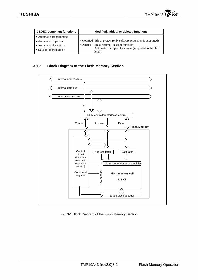
3.1.2 Block Diagram of the Flash Memory Section
Fig. 3-1 Block Diagram of the Flash Memory Section
Internal address bus
ROM controller/interleave control
Control Address Data Flash Memory
Column decoder/sense amplifier
Data latchAddress latch
Erase block decoder
Control circuit
(includes automatic sequence control)
Command
register
Internal data bus
Internal control bus
Flash memory cell
512 KB
Row
dec
ode
r

TMP19A43
TMP19A43 (rev2.0)3-3 Flash Memory Operation
3.2 Operation Mode
This device has three operation modes including the mode not to use the internal flash memory.
Table 3-1 Operation Modes
Operation mode Operation details
Single chip mode
After reset is cleared, it starts up from the internal flash memory.
Normal mode In this operation mode, two different modes, i.e., the mode to execute user application programs and the mode to rewrite the flash memory onboard the user’s card, are defined. The former is referred to as "normal mode" and the latter "user boot mode."
User boot mode The user can uniquely configure the system to switch between these two modes. For example, the user can freely design the system such that the normal mode is selected when the port "00" is set to "1" and the user boot mode is selected when it is set to "0." The user should prepare a routine as part of the application program to make the decision on the selection of the modes.
Single boot mode After reset is cleared, it starts up from the internal Boot ROM (Mask ROM). In the Boot ROM, an algorithm to enable flash memory rewriting on the user’s set through the serial port of this device is programmed. By connecting to an external host computer through the serial port, the internal flash memory can be programmed by transferring data in accordance with predefined protocols.
Among the flash memory operation modes listed in the above table, the User Boot mode and the Single Boot mode are the programmable modes. These two modes, the User Boot mode and the Single Boot mode, are referred to as "Onboard Programming" modes where onboard rewriting of internal flash memory can be made on the user's card.

TMP19A43
TMP19A43 (rev2.0)3-4 Flash Memory Operation
Either the Single Chip or Single Boot operation mode can be selected by externally setting the level of the BOOT input pin while the device is in reset status.
After the level is set, the CPU starts operation in the selected operation mode when the reset condition is removed. Regarding the TEST0, TEST1, and BOOT pins, be sure not to change the levels during operation once the mode is selected.
The mode setting method and the mode transition diagram are shown below:
Table 3-2 Operation Mode Setting
Input pin Operation mode
RESET BOOT Single chip mode 0 to 1 1 Single boot mode 0 to 1 0
Fig. 3-2 Mode Transition Diagram
3.2.1 Reset Operation
To reset the device, ensure that the power supply voltage is within the operating voltage range, that the internal oscillator has been stabilized, and that the RESET input is held at "0" for a minimum duration of 12 system clocks (2.4 µs with 40MHz operation; the "1/8" clock gear mode is applied after reset).
(Note 1) Regarding power-on reset of devices with internal flash memory;
For devices with internal flash memory, it is necessary to apply "0" to the RESET inputs upon power on for a minimum duration of 500 microseconds regardless of the operating frequency.
(Note 2) While flash programming or deletion is in progress, at least 0.5 microseconds of reset period is required regardless of the system clock frequency.
Onboard Programming mode
User to set the switch method
Single chip mode
Reset state
Normal mode User
Boot mode
Single Boot mode

TMP19A43
TMP19A43 (rev2.0)3-5 Flash Memory Operation
3.2.2 DSU (EJTAG) - PROBE Interface
This interface is used when the DSU probe is used in debugging. This is the dedicated interface for connection to the DSU probe. Please refer to the operation manual for the DSU probe you are going to use for details of debugging procedures to use the DSU probe. Here, the function to enable/disable the DSU probe in the DSU (EJTAG) mode is described.
1) Protect function
This device allows use of on-board DSU probes for debugging. To facilitate this, the device is implemented with a protection function to prevent easy reading of the internal flash memory by a third party other than the authorized user. By enabling the protection function, it becomes impossible to read the internal flash memory from a DSU probe. Use this function together with the protection function of the internal flash memory itself as described later.
2) DSU probe enable/disable function
This device allows use of on-board DSU probes for debugging operations. To facilitate this, the device is implemented with the "DSU probe inhibit" function (hereafter referred to as the "DSU
inhibit" function) to prevent easy reading of the internal flash memory by a third party other than the authorized user. By enabling the DSU inhibit function, use of any DSU probe becomes impossible.
3) DSU enable (Enables use of DSU probes for debugging)
In order to prevent the DSU inhibit function from being accidentally removed by system runaway, etc., the method to cancel the DSU inhibit function is in double protection structure so it is necessary to set SEQMOD <DSUOFF> to "0" and also write the protect code "0x0000_00C5" to the DSU protect control register SEQCNT to cancel the function. Then, debugging to use a DSU probe can be allowed. While power to the device is still applied, setting SEQMOD <SEQON> to "1" and writing "0x0000_00C5" to the SEQCNT register will enable the protection function again.
Table 3-3 DSU Protect Mode Register
7 6 5 4 3 2 1 0
SEQMOD Bit Symbol DSUOFF
(0xFFFF_E510) Read/Write R R/W
After reset 0 1
Function Always reads "0." 1: DSU disable
0: DSU available
15 14 13 12 11 10 9 8
Bit Symbol
Read/Write R
After reset 0
Function Always reads "0."
23 22 21 20 19 18 17 16
Bit Symbol
Read/Write R
After reset 0
Function
31 30 29 28 27 26 25 24
Bit Symbol
Read/Write R
After reset 0
Function Always reads "0."
(Note) This register must be 32-bit accessed.
(note)This register is initialized only by power-on reset. It is not initialized in reset usually. (FLASH)

TMP19A43
TMP19A43 (rev2.0)3-6 Flash Memory Operation
Table 3-4 DSU Protect Control Register
7 6 5 4 3 2 1 0
SEQCNT Bit Symbol
(0xFFFF_E514) Read/Write W
After reset
Function Write "0x0000_00C5."
15 14 13 12 11 10 9 8
Bit Symbol
Read/Write W
After reset
Function Write "0x0000_00C5."
23 22 21 20 19 18 17 16
Bit Symbol
Read/Write W
After reset
Function Write "0x0000_00C5."
31 30 29 28 27 26 25 24
Bit Symbol
Read/Write W
After reset
Function Write "0x0000_00C5."
(Note 1) This register must be 32-bit accessed.
4) Example use by the user
An example to use a DSU probe together with this function is shown as follows:
Figure 3-3 Example Use of DSU Inhibit Function
[DSU-Probe available] DSU can be used until power is turned off.
Power ON
DSU availability decision program(to be prepared by the user)
DSU inhibit cleared?
Clear DSU inhibit function by writing to SEQMOD and SEQCN[DSU-Probe disabled]
DSU remains unavailable
Y
N
External ports Data, etc.
Protection bit set to 1111
Y
N[DSU-Probe available]
Clear ROM protection (only for internal ROM/flash)

TMP19A43
TMP19A43 (rev2.0)3-7 Flash Memory Operation
(1-A) Method 1: Storing a Programming Routine in the Flash Memory
(1) Determine the conditions (e.g., pin states) required for the flash memory to enter User Boot mode and the I/O bus to be used to transfer new program code. Create hardware and software accordingly. Before installing the TMP19A43FDXBG on a printed circuit board, write the following program routines into an arbitrary flash block using programming equipment.
• Mode judgment routine: Code to determine whether or not to switch to User Boot mode
• Programming routine: Code to download new program code from a host controller and re-program the flash memory
• Copy routine: Code to copy the flash programming routine from the TMP19A43FDXBG flash memory to either the TMP19A43FDXBG on-chip RAM or external memory device.
(2) After RESET is released, the reset procedure determines whether to put the TMP19A43FDXBG flash memory in User Boot mode. If mode switching conditions are met, the flash memory enters User Boot mode. (All interrupts including NMI must be globally disabled while in User Boot mode.)
TMP19A43FDXBG
Flash Memory
RAM
[Reset Procedure]
(a) Mode Judgment Routine
Old Application Program Code
Host Controller New Application Program Code
I/O
(b) Programming Routine
(c) Copy Routine
TMP19A43FDXBG
Flash Memory
RAM
[Reset Procedure]
Old Application Program Code
Host Controller New Application Program Code
I/O
(a) Mode Judgment Routine
(b) Programming Routine
(c) Copy Routine
0 → 1 RESET
Conditions for entering User Boot mode (defined by the user)
User Boot Mode

TMP19A43
TMP19A43 (rev2.0)3-8 Flash Memory Operation
(3) Once User Boot mode is entered, execute the copy routine to copy the flash programming routine to either the TMP19A43FDXBG on-chip RAM or an external memory device. (In the following figure, the on-chip RAM is used.)
(4) Jump program execution to the flash programming routine in the on-chip RAM to erase a flash block containing the old application program code.
TMP19A43FDXBG
Flash Memory
RAM
[Reset Procedure]
(a) Mode Judgment Routine
Old Application Program Code
Host Controller New Application Program Code
I/O
(b) Programming Routine
(c) Copy Routine
(b) Programming Routine
TMP19A43FDXBG
Flash Memory
RAM
[Reset Procedure]
(a) Mode Judgment Routine
Host Controller New Application Program Code
I/O
(b) Programming Routine
(c) Copy Routine
(b) Programming Routine
Erased

TMP19A43
TMP19A43 (rev2.0)3-9 Flash Memory Operation
(5) Continue executing the flash programming routine to download new program code from the host controller and program it into the erased flash block. Once programming is complete, turn on the protection of that flash block.
(6) Drive RESET low to reset the TMP19A43FDXBG. Upon reset, the on-chip flash memory is put in Normal mode. After RESET is released, the CPU will start executing the new application program code.
TMP19A43FDXBG
Flash Memory
RAM
[Reset Procedure]
(a) Mode Judgment Routine
New Application Program Code
Host Controller New Application Program Code
I/O
(b) Programming Routine
(c) Copy Routine
(b) Programming Routine
TMP19A43FDXBG
Flash Memory
RAM
[Reset Procedure]
(a) Mode Judgment Routine
New Application Program Code e
Host Controller
(I/O)
(b) Programming Routine
(c) Copy Routine
0 → 1 RESET
Set to Normal mode

TMP19A43
TMP19A43 (rev2.0)3-10 Flash Memory Operation
(1-B) Method 2: Transferring a Programming Routine from an External Host
(1) Determine the conditions (e.g., pin states) required for the flash memory to enter User Boot mode and the I/O bus to be used to transfer new program code. Create hardware and software accordingly. Before installing the TMP19A43FDXBG on a printed circuit board, write the following program routines into an arbitrary flash block using programming equipment.
Mode judgment routine: Code to determine whether or not to switch to User Boot mode
Transfer routine: Code to download new program code from a host controller
Also, prepare a programming routine on the host controller:
Programming routine: Code to download new program code from an external host controller and re-program the flash memory
(2) After RESET is released, the reset procedure determines whether to put the TMP19A43FDXBG flash memory in User Boot mode. If mode switching conditions are met, the flash memory enters User Boot mode. (All interrupts including NMI must be globally disabled while in User Boot mode.)
TMP19A43FDXBG
Flash Memory
RAM
[Reset Procedure]
(a) Mode Judgment Routine
Old Application Program Code
Host Controller New Application Program Code
I/O
(b) Transfer Routine
(c) Programming Routine
TMP19A43FDXBG
Host Controller
I/O
0 → 1 RESET
Conditions for entering User Boot mode (defined by the user)
Flash Memory
RAM
[Reset Procedure]
(a) Mode Judgment Routine
Old Application Program Code
(b) Transfer Routine
New Application Program Code
(c) Programming Routine

TMP19A43
TMP19A43 (rev2.0)3-11 Flash Memory Operation
(3) Once User Boot mode is entered, execute the transfer routine to download the flash programming routine from the host controller to either the TMP19A43FDXBG on-chip RAM or an external memory device. (In the following figure, the on-chip RAM is used.)
(4) Jump program execution to the flash programming routine in the on-chip RAM to erase a flash block containing the old application program code.
TMP19A43FDXBG
Flash Memory
RAM
[Reset Procedure]
(a) Mode Judgment Routine
Old Application Program Code
Host Controller New Application Program Code
I/O
(b) Transfer Routine
(c) Programming Routine
(c) Programming routine
TMP19A43FDXBG
Flash Memory
RAM
[Reset Procedure]
(a) Mode Judgment Routine
Host Controller New Application Program Code
I/O
(b) Transfer Routine
(c) Programming Routine
(c) Programming RoutineErased

TMP19A43
TMP19A43 (rev2.0)3-12 Flash Memory Operation
(5) Continue executing the flash programming routine to download new program code from the host controller and program it into the erased flash block. Once programming is complete, turn on the protection of that flash block.
Drive RESET low to reset the TMP19A43FDXBG. Upon reset, the on-chip flash memory is put in Normal mode. After RESET is released, the CPU will start executing the new application program code.
TMP19A43FDXBG
Flash Memory
RAM
[Reset Procedure]
(a) Mode Judgment Routine
New Application Program Code
Host Controller New Application Program Code
I/O
(b) Transfer Routine
(c) Programming Routine
(c) Programming Routine
TMP19A43FDXBG
Host Controller
I/O
0 → 1 RESET
Set to Normal mode
Flash Memory
RAM
[Reset Procedure]
(a) Mode Judgment Routine
New Application Program Code
(b) Transfer Routine

TMP19A43
TMP19A43 (rev2.0)3-13 Flash Memory Operation
3.3 Single Boot Mode
In Single Boot mode, the flash memory can be re-programmed by using a program contained in the TMP19A43FDXBG on-chip boot ROM. This boot ROM is a masked ROM. When Single Boot mode is selected upon reset, the boot ROM is mapped to the address region including the interrupt vector table while the flash memory is mapped to an address region different from it.
Single Boot mode allows for serial programming of the flash memory. Channel 0 of the SIO (SIO0) of the TMP19A43FDXBG is connected to an external host controller. Via this serial link, a programming routine is downloaded from the host controller to the TMP19A43FDXBG on-chip RAM. Then, the flash memory is re-programmed by executing the programming routine. The host sends out both commands and programming data to re-program the flash memory.
Communications between the SIO0 and the host must follow the protocol described later. To secure the contents of the flash memory, the validity of the application’s password is checked before a programming routine is downloaded into the on-chip RAM. If password matching fails, the transfer of a programming routine itself is aborted.
As in the case of User Boot mode, all interrupts including the nonmaskable (NMI) interrupt must be globally disabled in Single Boot mode while the flash memory is being erased or programmed. In Single Boot mode, the boot-ROM programs are executed in Normal mode.
Once re-programming is complete, it is recommended to protect relevant flash blocks from accidental corruption during subsequent Single-Chip (Normal mode) operations. For a detailed description of the erase and program sequence, refer to On-Board Programming and Erasure.

TMP19A43
TMP19A43 (rev2.0)3-14 Flash Memory Operation
(2-A) General Procedure: Using the Program in the On-Chip Boot ROM
(1) The flash block containing the older version of the program code need not be erased before executing the programming routine. Since a programming routine and programming data are transferred via the SIO0, the SIO0 must be connected to a host controller. Prepare a programming routine on the host controller.
(2) Reset the TMP19A43FDXBG with the mode setting pins held at appropriate logic values, so that the CPU re-boots from the on-chip boot ROM. The 12-byte password transferred from the host controller is first compared to the contents of special flash memory locations. (If the flash block has already been erased, the password is 0xFFFF.)
TMP19A43FDXBG
Flash Memory
RAM
Old Application Program Code (or Erased State)
Host Controller New Application Program Code
I/O(a) Programming Routine
Boot ROM SIO0
TMP19A43FDXBG
Host Controller
I/O
0 → 1 RESET
Conditions for entering Single Boot mode
New Application Program Code
(a) Programming Routine
Flash Memory
RAM
Old Application Program Code (or Erased State)
Boot ROM SIO0
Boot Mode
TMP19A43
TMP19A43 (rev2.0)3-15 Flash Memory Operation
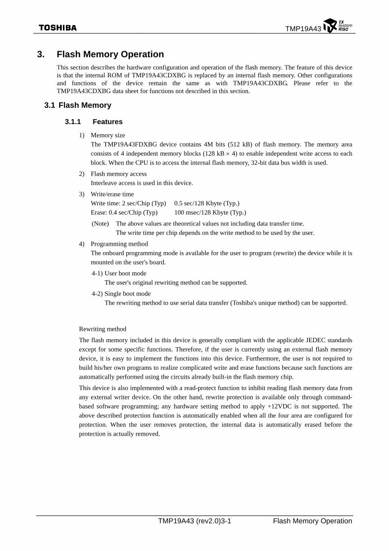
If the password was correct, the boot program downloads, via the SIO0, the programming routine from the host controller into the on-chip RAM of the TMP19A43FDXBG. The programming routine must be stored in the address range 0xFFFD_6000 – 0xFFFD_EFFF.
(3) The CPU jumps to the programming routine in the on-chip RAM to erase the flash block containing the old application program code. The Block Erase or Chip Erase command may be used.
TMP19A43FDXBG
Flash Memory
RAM
Old Application Program Code (or Erased State)
Host Controller New Application Program Code
I/O(a) Programming routine
Boot ROM SIO0
(a) Programming Routine
TMP19A43FDXBG
Flash Memory
RAM
Host Controller New Application Program Code
I/O(a) Programming routine
Boot ROM SIO0
(a) Programming Routine
Erased

TMP19A43
TMP19A43 (rev2.0)3-16 Flash Memory Operation
Next, the programming routine downloads new application program code from the host controller and programs it into the erased flash block. Once programming is complete, protection of that flash block is turned on.
It is not allowed to move program control from the programming routine back to the boot ROM.
In the example below, new program code comes from the same host controller via the same SIO channel as for the programming routine. However, once the programming routine has begun to execute, it is free to change the transfer path and the source of the transfer. Create board hardware and a programming routine to suit your particular needs.
(4) When programming of the flash memory is complete, power off the board and disconnect the cable leading from the host to the target board. Turn on the power again so that the TMP19A43FDXBG re-boots in Single-Chip (Normal) mode to execute the new program.
TMP19A43FDXBG
Flash Memory
RAM
New Application Program Code
Host Controller New Application Program Code
I/O(a) Programming Routine
Boot ROM SIO0
(a) Programming Routine
TMP19A43FDXBG
Host Controller
0 → 1 RESET
Set to Single-Chip (Normal) mode
Flash Memory
RAM
New Application Program Code
Boot ROM SIO0

TMP19A43
TMP19A43 (rev2.0)3-17 Flash Memory Operation
3.3.1 Configuring for Single Boot Mode
For on-board programming, boot the TMP19A43FDXBG in Single Boot mode, as follows: BOOT = 0
RESET = 0 → 1
Set the RESET input at logic 0, and the BW0, BW1 and BOOT inputs at the logic values shown above, and then release RESET (high).
3.3.2 Memory Map
Figure 3.1 shows a comparison of the memory maps in Normal and Single Boot modes. In single Boot mode, the on-chip flash memory is mapped to physical addresses (0x4000_0000 through 0x4007_FFFF), virtual addresses (0x0000_0000 through 0x0007_FFFF), and the on-chip boot ROM is mapped to physical addresses 0x1FC0_0000 through 0x1FC0_1FFF.
Figure 3.1 Memory Maps for Normal and Single Boot Modes (Physical Addresses)
On-Chip Peripherals
Normal Mode Single Boot Mode
0x1FC0_1FFF
0x1FC0_0000
0x0000_0000
0xFFFF_FFFF
0xFFFF_DFFF
0xFFFF_8000
0xFF3F_FFFF
0xFF20_0000
0xC000_0000
0x400F_FFFF
0x4000_0000
0x1FC7_FFFF
0x1FC0_0500
0x1FC0_0000
0x2000_0000
0x0000_0000
0xFF00_0000
0xBF00_0000
0xFFFF_FFFF
0xFFFF_DFFF
0xFFFF_8000
0xFF3F_FFFF
0xFF20_0000
0xC000_0000
0x4007_FFFF
0x4000_0000
0x2000_0000
0xFF00_0000
0xBF00_0000
On-Chip RAM (24 KB)
(Reserved)
Used for debugging
(Reserved)
(Reserved)
(Reserved)
On-Chip ROM Shadow
Inaccessible
(512 MB)
User Program Area
Maskable Interrupt Area
Exception Vector Area
On-Chip Peripherals
On-Chip RAM (24 KB)
(Reserved)
Used for debugging (Reserved)
(Reserved)
(Reserved)
On-Chip Flash ROM
Inaccessible (512 MB)
Boot ROM (6 KB)
Internal ROM

TMP19A43
TMP19A43 (rev2.0)3-18 Flash Memory Operation
3.3.3 Interface Specification
In Single Boot mode, an SIO channel is used for communications with a programming controller. Both UART (asynchronous) and I/O Interface (synchronous) modes are supported. The communication formats are shown below. In the subsections that follow, virtual addresses are indicated, unless otherwise noted.
• UART mode
Communication channel: SIO Channel 0 (SIO0) Transfer mode: UART (asynchronous) mode, full-duplex Data length: 8 bits Parity bits: None STOP bits: 1 Baud rate: Arbitrary baud rate
• I/O Interface mode
Communication channel: SIO Channel 0 (SIO0) Transfer mode: I/O Interface mode, half-duplex Synchronization clock (SCLK0): Input Handshaking signal: P67 configured as an output Baud rate: Arbitrary baud rate
Table 3.1 Required Pin Connections
Interface Pin
UART Mode I/O Interface Mode
DVCC15 Required Required Power Supply Pins
DVSS Required Required
Mode-Setting Pin BOOT Required Required
Reset Pin RESET Required Required
TXD0 Required Required
RXD0 Required Required
SCLK0 Not Required Required (Input Mode)
Communication Pins
P67 Not Required Required (OUTPUT Mode)
3.3.4 Data Transfer Format
The host controller is to issue one of the commands listed in Table 3.2
to the target board. Table 3.3 to Table 3.5 illustrate the sequence of two-way communications that should occur in response to each command.
Table 3.2 Single Boot Mode Commands
Code Command
10H RAM Transfer
20H Show Flash Memory Sum
30H Show Product Information

TMP19A43
TMP19A43 (rev2.0)3-19 Flash Memory Operation
Table 3.3 Transfer Format for the RAM Transfer Command
Byte Data Transferred from the Controller
to the TMP19A43FDXBG Baud Rate
Data Transferred from the TMP19A43FDXBG to the Controller
Boot ROM 1st byte Serial operation mode and baud rate
For UART mode 86H
For I/O Interface mode 30H
Desired baud rate (Note 1)
⎯
2nd byte ⎯ ACK for the serial operation mode byte
For UART mode
Normal acknowledge 86H
(The boot program aborts if the baud rate is can not be set correctly.)
For I/O Interface mode
Normal acknowledge 30H
3rd byte Command code (10H) ⎯
4th byte ⎯ ACK for the command code byte (Note 2)
Normal acknowledge 30H
Negative acknowledge x1H
Communication error x8H
5th byte
thru
16th byte
Password sequence (12 bytes) (0x4000_0474 thru 0x4000_047F)
⎯
17th byte Checksum value for bytes 5–16 ⎯
18th byte ⎯ ACK for the checksum byte (Note 2)
Normal acknowledge 10H
Negative acknowledge x1H
Communication error x8H
19th byte RAM storage start address (bits 31–24) ⎯
20th byte RAM storage start address (bits 23–16) ⎯
21st byte RAM storage start address (bits 15–8) ⎯
22nd byte RAM storage start address (bits 7–0) ⎯
23rd byte RAM storage byte count (bits 15–8) ⎯
24th byte RAM storage byte count (bits 7–0) ⎯
25th byte Checksum value for bytes 19–24 ⎯
26th byte ⎯ ACK for the checksum byte (Note 2)
Normal acknowledge 10H
Negative acknowledge x1H
Communication error x8H
27th byte
thru
mth byte
RAM storage data ⎯
(m + 1)th byte Checksum value for bytes 27–m ⎯
(m + 2)th byte ⎯ ACK for the checksum byte (Note 2)
Normal acknowledge 10H
Non-acknowledge x1H
Communications error x8H
RAM (m + 3)th byte ⎯ Jump to RAM storage start address
Note 1: In I/O Interface mode, the baud rate for the transfers of the first and second bytes must be 1/16 of the desired baud rate.
Note 2: In case of any negative acknowledge, the boot program returns to a state in which it waits for a command code (3rd byte). In I/O Interface mode, if a communication error occurs, a negative acknowledge does not occur.
Note 3: The 19th to 25th bytes must be within the RAM address range 0xFFFD_8000–0xFFFF_CFFF

TMP19A43
TMP19A43 (rev2.0)3-20 Flash Memory Operation
Table 3.4 Transfer Format for the Show Flash Memory Sum Command
Byte Data Transferred from the Controller
to the TMP19A43FDXBG Baud Rate
Data Transferred from the TMP19A43FDXBG to the Controller
Boot ROM 1st byte Serial operation mode and baud rate
For UART mode 86H
For I/O Interface mode 30H
Desired baud rate (Note 1)
⎯
2nd byte ⎯ ACK for the serial operation mode byte
For UART mode
Normal acknowledge 86H
(The boot program aborts if the baud rate can not be set correctly.)
For I/O Interface mode
Normal acknowledge 30H
3rd byte Command code (20H) ⎯
4th byte ⎯ ACK for the command code byte (Note 2)
Normal acknowledge 20H
Negative acknowledge x1H
Communication error x8H
5th byte ⎯ SUM (upper byte)
6th byte ⎯ SUM (lower byte)
7th byte ⎯ Checksum value for bytes 5 and 6
8th byte (Wait for the next command code.) ⎯
Note 1: In I/O Interface mode, the baud rate for the transfers of the first and second bytes must be 1/16 of the desired baud rate.
Note 2: In case of any negative acknowledge, the boot program returns to a state in which it waits for a command code (3rd byte). In I/O Interface mode, if a communication error occurs, a negative acknowledge does not occur.

TMP19A43
TMP19A43 (rev2.0)3-21 Flash Memory Operation
Table 3.5 Transfer Format for the Show Product Information Command (1/2)
Byte Data Transferred from the Controller
to the TMP19A43FDXBG Baud Rate
Data Transferred from the TMP19A43FDXBG to the Controller
Boot ROM 1st byte Serial operation mode and baud rate For UART mode 86H For I/O Interface mode 30H
⎯
2nd byte ⎯
Desired baud rate (Note 1)
ACK for the serial operation mode byte For UART mode Normal acknowledge 86H
(The boot program aborts if the baud rate can not be set correctly.)
For I/O Interface mode Normal acknowledge 30H
3rd byte Command code (30H) ⎯
4th byte ⎯ ACK for the command code byte (Note 2) Normal acknowledge 10H Negative acknowledge x1H Communication error x8H
5th byte ⎯ Flash memory data (at address 0x4000_0470)
6th byte ⎯ Flash memory data (at address 0x4000_0471)
7th byte ⎯ Flash memory data (at address 0x4000_0472)
8th byte ⎯ Flash memory data (at address 0x4000_0473)
9th byte thru 20th byte
⎯ Product name (12-byte ASCII code) “TX19A43FD” from the 9th byte
21st byte thru 24th byte
⎯ Password comparison start address (4 bytes)74H, 04H, 00H and 00H from the 21st byte
25th byte thru 28th byte
⎯ RAM start address (4 bytes) 00H, 80H, FFH and FFH from the 25th byte
29th byte thru 32nd byte
⎯ Dummy data (4 bytes) FFH, 8FH, FFH and FFH from the 29th byte
33rd byte thru 36th byte
⎯ RAM end address (4 bytes) FFH, DFH, FFH and FFH from the 33rd byte
37th byte thru 40th byte
⎯ Dummy data (4 bytes) 00H,90H, FFH and FFH from the 37th byte
41st byte thru 44th byte
⎯ Dummy data (4 bytes) FFH, CFH, FFH and FFH from the 41st byte
45th byte thru 46th byte
⎯ Fuse information (2 bytes) 00H and 00H from the 45th byte
47th byte thru 50th byte
⎯ Flash memory start address (4 bytes) 00H, 00H, 00H and 00H from the 47th byte
51st byte thru 54th byte
⎯ Flash memory end address (4 bytes) FFH, FFH, 07H and 00H from the 51st byte
55th byte thru 56th byte
⎯
Flash memory block count (2 bytes) 00H and 00H from at the 55th byte

TMP19A43
TMP19A43 (rev2.0)3-22 Flash Memory Operation
Table 3.5 Transfer Format for the Show Product Information Command (2/2)
Byte Data Transferred from the Controller
to the TMP19A43FDXBG Baud Rate
Data Transferred from the TMP19A43FDXBG to the Controller
57th byte thru 60th byte
⎯ Start address of a group of the same-size flash blocks (4 bytes) 00H, 00H, 00H and 00H from the 57th byte
Boot ROM 61st byte thru 64th byte
⎯ Size (in halfwords) of the same-size flash blocks (4 bytes) 00H, 00H, 01H and 00H from the 61st byte
65th byte ⎯ Number of flash blocks of the same size (1 byte) 04H
66th byte ⎯ Checksum value for bytes 5 to 65
67th byte (Wait for the next command code.)
⎯
3.3.5 Overview of the Boot Program Commands
When Single Boot mode is selected, the boot program is automatically executed on startup. The boot program offers these three commands, the details of which are provided on the following subsections.
• RAM Transfer command
The RAM Transfer command stores program code transferred from a host controller to the on-chip RAM and executes the program once the transfer is successfully completed. The maximum program size is 36 kbytes. The RAM storage start address must be within the range.
The RAM Transfer command can be used to download a flash programming routine of your own; this provides the ability to control on-board programming of the flash memory in a unique manner. The programming routine must utilize the flash memory command sequences described in Section 3.6.17
Before initiating a transfer, the RAM Transfer command checks a password sequence coming from the controller against that stored in the flash memory. If they do not match, the RAM Transfer command aborts.
Once the RAM Transfer command is complete, the whole on-chip RAM is accessible.
• Show Flash Memory Sum command
The Show Flash Memory Sum command adds the contents of the 512 kbytes of the flash memory together. The boot program does not provide a command to read out the contents of the flash memory. Instead, the Flash Memory Sum command can be used for software revision management.
• Show Product Information command
The Show Product Information command provides the product name, on-chip memory configuration and the like. This command also reads out the contents of the flash memory locations at addresses 0x0000_03F0 through 0x0000_03F3. In addition to the Show Flash Memory Sum command, these locations can be used for software revision management.
Note 1: In I/O Interface mode, the baud rate for the transfers of the first and second bytes must be 1/16 of the desired baud rate.
Note 2: In case of any negative acknowledge, the boot program returns to a state in which it waits for a command code (3rd byte). In I/O Interface mode, if a communication error occurs, a negative acknowledge does not occur.
TMP19A43
TMP19A43 (rev2.0)3-23 Flash Memory Operation
3.3.6 RAM Transfer Command
See Table 3.3.
(5) The 1st byte specifies which one of the two serial operation modes is used. For a detailed description of how the serial operation mode is determined, see Section 3.3.10. If it is determined as UART mode, the boot program then checks if the SIO0 is programmable to the baud rate at which the 1st byte was transferred. During the first-byte interval, the RXE bit in the SC0MOD register is cleared.
• To communicate in UART mode
Send, from the controller to the target board, 86H in UART data format at the desired baud rate. If the serial operation mode is determined as UART, then the boot program checks if the SIO0 can be programmed to the baud rate at which the first byte was transferred. If that baud rate is not possible, the boot program aborts, disabling any subsequent communications.
• To communicate in I/O Interface mode
Send, from the controller to the target board, 30H in I/O Interface data format at 1/16 of the desired baud rate. Also send the 2nd byte at the same baud rate. Then send all subsequent bytes at a rate equal to the desired baud rate.
In I/O Interface mode, the CPU sees the serial receive pin as if it were a general input port in monitoring its logic transitions. If the baud rate of the incoming data is high or the chip’s operating frequency ishigh, the CPU may not be able to keep up with the speed of logic transitions. To prevent such situations, the 1st and 2nd bytes must be transferred at 1/16 of the desired baud rate; then the boot program calculates 16 times that as the desired baud rate.
When the serial operation mode is determined as I/O Interface mode, the SIO0 is configured for SCLK Input mode. Beginning with the third byte, the controller must ensure that its AC timing restrictions are satisfied at the selected baud rate. In the case of I/O Interface mode, the boot program does not check the receive error flag; thus there is no such thing as error acknowledge (x8H).
(6) The 2nd byte, transmitted from the target board to the controller, is an acknowledge response to
the 1st byte. The boot program echoes back the first byte: 86H for UART mode and 30H for I/O Interface mode.
• UART mode
If the SIO0 can be programmed to the baud rate at which the 1st byte was transferred, the boot program programs the BR0CR and sends back 86H to the controller as an acknowledge. If the SIO0 is not programmable at that baud rate, the boot program simply aborts with no error indication.
Following the 1st byte, the controller should allow for a time-out period of five seconds. If it does not receive 86H within the alloted time-out period, the controller should give up the communication.
The boot program sets the RXE bit in the SC0MOD register to enable reception before loading the SIO transmit buffer with 86H.

TMP19A43
TMP19A43 (rev2.0)3-24 Flash Memory Operation
• I/O Interface mode
The boot program programs the SC0MOD0 and SC0CR registers to configure the SIO0 in I/O Interface mode (clocked by the rising edge of SCLK0), writes 30H to the SC0BUF. Then, the SIO0 waits for the SCLK0 signal to come from the controller. Following the transmission of the 1st byte, the controller should send the SCLK clock to the target board after a certain idle time (several microseconds). This must be done at 1/16 the desire baud rate. If the 2nd byte, which is from the target board to the controller, is 30H, then the controller should take it as a go-ahead. The controller must then delivers the 3rd byte to the target board at a rate equal to the desired baud rate. The boot program sets the RXE bit in the SC0MOD register to enable reception before loading the SIO transmit buffer with 30H.
• (7) The 3rd byte, which the target board receives from the controller, is a command. The code for the
RAM Transfer command is 10H. • (8) The 4th byte, transmitted from the target board to the controller, is an acknowledge response to the
3rd byte. Before sending back the acknowledge response, the boot program checks for a receive error. If there was a receive error, the boot program transmits x8H and returns to the state in which it waits for a command again. In this case, the upper four bits of the acknowledge response are undefined — they hold the same values as the upper four bits of the previously issued command. When the SIO0 is configured for I/O Interface mode, the boot program does not check for a receive error.
If the 3rd byte is equal to any of the command codes listed in Table 3.2, the boot program echoes it back to the controller. When the RAM Transfer command was received, the boot program echoes back a value of 10H and then branches to the RAM Transfer routine. Once this branch is taken, a password check is done. Password checking is detailed in Section 3.3.11.
If the 3rd byte is not a valid command, the boot program sends back x1H to the controller and returns to the state in which it waits for a command again. In this case, the upper four bits of the acknowledge response are undefined — they hold the same values as the upper four bits of the previously issued command.
• (9) The 5th to 16th bytes, which the target board receives from the controller, are a 12-byte password.
The 5th byte is compared to the contents of address 0x0000_03F4 in the flash memory; the 6th byte is compared to the contents of address 0x0000_03F5 in the flash memory; likewise, the 16th byte is compared to the contents of address 0x0000_03FF in the flash memory. If the password checking fails, the RAM Transfer routine sets the password error flag.
• (10) The 17th byte is a checksum value for the password sequence (5th to 16th bytes). To calculate the
checksum value for the 12-byte password, add the 12 bytes together, drop the carries and take the two’s complement of the total sum. Transmit this checksum value from the controller to the target board. The checksum calculation is described in details in Section 3.3.13.

TMP19A43
TMP19A43 (rev2.0)3-25 Flash Memory Operation
(11) The 18th byte, transmitted from the target board to the controller, is an acknowledge response to the 5th to 17th bytes.
First, the RAM Transfer routine checks for a receive error in the 5th to 17th bytes. If there was a receive error, the boot program sends back 18H and returns to the state in which it waits for a command (i.e., the 3rd byte) again. In this case, the upper four bits of the acknowledge response are the same as those of the previously issued command (i.e., all 1s). When the SIO0 is configured for I/O Interface mode, the RAM Transfer routine does not check for a receive error.
Next, the RAM Transfer routine performs the checksum operation to ensure data integrity. Adding the series of the 5th to 17th bytes must result in zero (with the carry dropped). If it is not zero, one or more bytes of data has been corrupted. In case of a checksum error, the RAM Transfer routine sends back 11H to the controller and returns to the state in which it waits for a command (i.e., the 3rd byte) again.
Finally, the RAM Transfer routine examines the result of the password check. The following two cases are treated as a password error. In these cases, the RAM Transfer routine sends back 11H to the controller and returns to the state in which it waits for a command (i.e., the 3rd byte) again.
• Irrespective of the result of the password comparison, all of the 12 bytes of a password in the flash memory are the same value other than FFH.
• Not all of the password bytes transmitted from the controller matched those contained in the flash memory.
When all the above checks have been successful, the RAM Transfer routine returns a normal acknowledge response (10H) to the controller.
(12) The 19th to 22nd bytes, which the target board receives from the controller, indicate the start
address of the RAM region where subsequent data (e.g., a flash programming routine) should be stored. The 19th byte corresponds to bits 31–24 of the address, and the 22nd byte corresponds to bits 7–0 of the address.
(13) The 23rd and 24th bytes, which the target board receives from the controller, indicate the number
of bytes that will be transferred from the controller to be stored in the RAM. The 23rd byte corresponds to bits 15–8 of the number of bytes to be transferred, and the 24th byte corresponds to bits 7–0 of the number of bytes.
(14) The 25th byte is a checksum value for the 19th to 24th bytes. To calculate the checksum value, add
all these bytes together, drop the carries and take the two’s complement of the total sum. Transmit this checksum value from the controller to the target board. The checksum calculation is described in details in Section 3.3.13.
(15) The 26th byte, transmitted from the target board to the controller, is an acknowledge response to
the 19th to 25th bytes of data.First, the RAM Transfer routine checks for a receive error in the 19th to 25th bytes. If there was a receive error, the RAM Transfer routine sends back 18H and returns to the state in which it waits for a command (i.e., the 3rd byte) again. In this case, the upper four bits of the acknowledge response are the same as those of the previously issued command (i.e., all 1s). When the SIO0 is configured for I/O Interface mode, the RAM Transfer routine does not check for a receive error.
Next, the RAM Transfer routine performs the checksum operation to ensure data integrity. Adding the series of the 19th to 25th bytes must result in zero (with the carry dropped). If it is not zero, one or more bytes of data has been corrupted. In case of a checksum error, the RAM Transfer routine sends back 11H to the controller and returns to the state in which it waits for a command (i.e., the 3rd byte) again.

TMP19A43
TMP19A43 (rev2.0)3-26 Flash Memory Operation
• The RAM storage start address must be within the range 0xFFFD_6000–0xFFFD_EFFF.
When the above checks have been successful, the RAM Transfer routine returns a normal acknowledge response (10H) to the controller.
(16) The 27th to mth bytes from the controller are stored in the on-chip RAM of the
TMP19A43FDXBG. Storage begins at the address specified by the 19th–22nd bytes and continues for the number of bytes specified by the 23rd–24th bytes.
(17) The (m+1)th byte is a checksum value. To calculate the checksum value, add the 27th to mth bytes
together, drop the carries and take the two’s complement of the total sum. Transmit this checksum value from the controller to the target board. The checksum calculation is described in details in Section 3.3.13.
(18) The (m+2)th byte is a acknowledge response to the 27th to (m+1)th bytes.
First, the RAM Transfer routine checks for a receive error in the 27th to (m+1)th bytes. If there was a receive error, the RAM Transfer routine sends back 18H and returns to the state in which it waits for a command (i.e., the 3rd byte) again. In this case, the upper four bits of the acknowledge response are the same as those of the previously issued command (i.e., all 1s). When the SIO0 is configured for I/O Interface mode, the RAM Transfer routine does not check for a receive error.
(19) Next, the RAM Transfer routine performs the checksum operation to ensure data integrity. Adding the series of the 27th to (m+1)th bytes must result in zero (with the carry dropped). If it is not zero, one or more bytes of data has been corrupted. In case of a checksum error, the RAM Transfer routine sends back 11H to the controller and returns to the state in which it waits for a command (i.e., the 3rd byte) again. When the above checks have been successful, the RAM Transfer routine returns a normal acknowledge response (10H) to the controller. If the (m+2)th byte was a normal acknowledge response, a branch is made to the address specified by the 19th to 22nd bytes in 32-bit ISA mode.
3.3.7 Show Flash Memory Sum Command
See Table 3.4.
(20) The processing of the 1st and 2nd bytes are the same as for the RAM Transfer command.
(21) The 3rd byte, which the target board receives from the controller, is a command. The code for the Show Flash Memory Sum command is 20H.
(22) The 4th byte, transmitted from the target board to the controller, is an acknowledge response to the
3rd byte. Before sending back the acknowledge response, the boot program checks for a receive error. If there was a receive error, the boot program transmits x8H and returns to the state in which it waits for a command again. In this case, the upper four bits of the acknowledge response are undefined — they hold the same values as the upper four bits of the previously issued command. When the SIO0 is configured for I/O Interface mode, the boot program does not check for a receive error.
If the 3rd byte is equal to any of the command codes listed in Table 3.2 on page 3-18, the boot program echoes it back to the controller. When the Show Flash Memory Sum command was received, the boot program echoes back a value of 20H and then branches to the Show Flash Memory Sum routine.
TMP19A43
TMP19A43 (rev2.0)3-27 Flash Memory Operation
If the 3rd byte is not a valid command, the boot program sends back x1H to the controller and returns to the state in which it waits for a command again. In this case, the upper four bits of the acknowledge response are undefined — they hold the same values as the upper four bits of the previously issued command.
(23) The Show Flash Memory Sum routine adds all the bytes of the flash memory together. The 5th and
6th bytes, transmitted from the target board to the controller, indicate the upper and lower bytes of this total sum, respectively. For details on sum calculation, see Section 3.3.12.
(24) The 7th byte is a checksum value for the 5th and 6th bytes. To calculate the checksum value, add
the 5th and 6th bytes together, drop the carry and take the two’s complement of the sum. Transmit this checksum value from the controller to the target board.
(25) The 8th byte is the next command code.
3.3.8 Show Product Information Command
See Table 3.5.
(26) The processing of the 1st and 2nd bytes are the same as for the RAM Transfer command.
(27) The 3rd byte, which the target board receives from the controller, is a command. The code for the
Show Product Information command is 30H.
(28) The 4th byte, transmitted from the target board to the controller, is an acknowledge response to the
3rd byte. Before sending back the acknowledge response, the boot program checks for a receive error. If there was a receive error, the boot program transmits x8H and returns to the state in which it waits for a command again. In this case, the upper four bits of the acknowledge response are undefined — they hold the same values as the upper four bits of the previously issued command. When the SIO0 is configured for I/O Interface mode, the boot program does not check for a receive error.
If the 3rd byte is equal to any of the command codes listed in Table 3.2 on page 3-18, the boot program echoes it back to the controller. When the Show Flash Memory Sum command was received, the boot program echoes back a value of 30H and then branches to the Show Flash Memory Sum routine.
If the 3rd byte is not a valid command, the boot program sends back x1H to the controller and returns to the state in which it waits for a command again. In this case, the upper four bits of the acknowledge response are undefined — they hold the same values as the upper four bits of the previously issued command.
(29) The 5th to 8th bytes, transmitted from the target board to the controller, are the data read from
addresses 0x0000_03F0–0x0000_03F3 in the flash memory. Software version management is possible by storing a software id in these locations.
(30) The 9th to 20th bytes, transmitted from the target board to the controller, indicate the product name,
which is “TX19A43FD_ _ _” in ASCII code (where _ is a space).
TMP19A43
TMP19A43 (rev2.0)3-28 Flash Memory Operation
(31) The 21st to 24th bytes, transmitted from the target board to the controller, indicate the start address of the flash memory area containing the password, i.e., F4H, 03H, 00H, 00H.
(32) The 25th to 28th bytes, transmitted from the target board to the controller, indicate the start address
of the on-chip RAM, i.e., 00H, 60H, FDH, FFH.
(33) The 29th to 32nd bytes, transmitted from the target board to the controller, are dummy data (FFH, 6FH, FDH, FFH).
(34) The 33rd to 36th bytes, transmitted from the target board to the controller, indicate the end address
of the on-chip RAM, i.e., FFH, FFH, FDH, FFH.
(35) The 37th to 40th bytes, transmitted from the target board to the controller, are 00H, 70H, FDH and FFH.
The 41st to 44th bytes, transmitted from the target board to the controller, are FFH, EFH, FDH and FFH.
(36) The 45th and 46th bytes, transmitted from the target board to the controller, indicate the presence
or absence of the security and protect bits and whether the flash memory is divided into blocks. Bit 0 indicates the presence or absence of the security bit; it is 0 if the security bit is available. Bit 1 indicates the presence or absence of the protect bits; it is 0 if the protect bits are available. If bit 2 is 0, it indicates that the flash memory is divided into blocks. The remaining bits are undefined. The 45th and 46th bytes are 01H, 00H.
(37) The 47th to 50th bytes, transmitted from the target board to the controller, indicate the start address
of the on-chip flash memory, i.e., 00H, 00H, 00H, 00H.
(38) The 51st to 54th bytes, transmitted from the target board to the controller, indicate the end address of the on-chip flash memory, i.e., FFH, FFH, 0FH, 00H.
(39) The 55th to 56th bytes, transmitted from the target board to the controller, indicate the number of
flash blocks available, i.e., 08H, 00H.
(40) The 57th to 92nd bytes, transmitted from the target board to the controller, contain information about the flash blocks.
Flash blocks of the same size are treated as a group. Information about the flash blocks indicate the start address of a group, the size of the blocks in that group (in halfwords) and the number of the blocks in that group.
The 57th to 65th bytes are the information about the 128-kbyte blocks (Block 0 to Block 7). See Table 3.5 for the values of bytes transmitted.
(41) The 66th byte, transmitted from the target board to the controller, is a checksum value for the 5th
to 65th bytes. The checksum value is calculated by adding all these bytes together, dropping the carry and taking the two’s complement of the total sum.
(42) The 67th byte is the next command code.
TMP19A43
TMP19A43 (rev2.0)3-29 Flash Memory Operation
3.3.9 Acknowledge Responses
The boot program represents processing states with specific codes. Table 3.6 to Table 3.8 show the values of possible acknowledge responses to the received data. The upper four bits of the acknowledge response are equal to those of the command being executed. Bit 3 of the code indicates a receive error. Bit 0 indicates an invalid command error, a checksum error or a password error. Bit 1 and bit 2 are always 0. Receive error checking is not done in I/O Interface mode.
Table 3.6 ACK Response to the Serial Operation Mode Byte
Return Value Meaning
86H The SIO can be configured to operate in UART mode. (See Note) 30H The SIO can be configured to operate in I/O Interface mode.
Table 3.7 ACK Response to the Command Byte
Return Value Meaning
x8H (See Note) A receive error occurred while getting a command code.
x1H (See Note) An undefined command code was received. (Reception was completed normally.)
10H The RAM Transfer command was received.
20H The Show Flash Memory Sum command was received.
30H The Show Product Information command was received.
Table 3.8 ACK Response to the Checksum Byte
Return Value Meaning
18H A receive error occurred.
11H A checksum or password error occurred.
10H The checksum was correct.
Note: If the serial operation mode is determined as UART, the boot program checks if the SIO can be programmed to the baud rate at which the operation mode byte was transferred. If that baud rate is not possible, the boot program aborts, without sending back any response.
Note: The upper four bits of the ACK response are the same as those of the previous command code.

TMP19A43
TMP19A43 (rev2.0)3-30 Flash Memory Operation
3.3.10 Determination of a Serial Operation Mode
The first byte from the controller determines the serial operation mode. To use UART mode for communications between the controller and the target board, the controller must first send a value of 86H at a desired baud rate to the target board. To use I/O Interface mode, the controller must send a value of 30H at 1/16 the desired baud rate. Figure 3.2 shows the waveforms for the first byte.
Figure 3.2 Serial Operation Mode Byte
After RESET is released, the boot program monitors the first serial byte from the controller, with the
SIO reception disabled, and calculates the intervals of tAB, tAC and tAD. Figure 3.3 shows a flowchart describing the steps to determine the intervals of tAB, tAC and tAD. As shown in the flowchart, the boot program captures timer counts each time a logic transition occurs in the first serial byte. Consequently, the calculated tAB, tAC and tAD intervals are bound to have slight errors. If the transfer goes at a high baud rate, the CPU might not be able to keep up with the speed of logic transitions at the serial receive pin. In particular, I/O Interface mode is more prone to this problem since its baud rate is generally much higher than that for UART mode. To avoid such a situation, the controller should send the first serial byte at 1/16 the desired baud rate.
The flowchart in Figure 3.4 shows how the boot program distinguishes between UART and I/O Interface modes. If the length of tAB is equal to or less than the length of tCD, the serial operation mode is determined as UART mode. If the legnth of tAB is greater than the length of tCD, the serial operation mode is determined as I/O Interface mode. Bear in mind that if the baud rate is too high or the timer operating frequency is too low, the timer resolution will be coarse, relative to the intervals between logic transitions. This becomes a problem due to inherent errors caused by the way in which timer counts are captured by software; consequently the boot program might not be able to determine the serial operation mode correctly.
For example, the serial operation mode may be determined to be I/O Interface mode when the intended mode is UART mode. To avoid such a situation, when UART mode is utilized, the controller should allow for a time-out period within which it expects to receive an echo-back (86H) from the target board. The controller should give up the communication if it fails to get that echo-back within the alloted time. When I/O Interface mode is utilized, once the first serial byte has been transmitted, the controller should send the SCLK clock after a certain idle time to get an acknowledge response. If the received acknowledge response is not 30H, the controller should give up further communications.
UART (86H)
tAB
Point A Point B Point C Point D bit 7 bit 0 bit 1 bit 2 bit 3 bit 4 bit 5 bit 6 Start Stop
tCD
I/O Interface (30H)
tAB
bit 7 bit 0 bit 1 bit 2 bit 3 bit 4 bit 5 bit 6
tCD
Point A Point B Point C Point D

TMP19A43
TMP19A43 (rev2.0)3-31 Flash Memory Operation
Figure 3.3 Serial Operation Mode Byte Reception Flow
Initialize 16-bit Timer 0 (φT1 = 8/fc, counter cleared)
Set TB0RG1 to 0xFFFF Prescaler is on.
16-bit Timer 0 starts counting up
Point A
Stop operation (infinite loop)
High-to-low transition on serial receive pin?
Yes
Yes
Yes
Start
Low-to-high transition on serial receive pin?
Software-capture and save timer value (tAB)
High-to-low transition on serial receive pin?
Software-capture and save timer value (tAC)
Yes
Low-to-high transition on serial receive pin?
Software-capture and save timer value (tAD)
16-bit Timer 0 stops counting
tAC ≥ tAD?
Make backup copy of tAD value
Done
Yes
Point B
Point C
Point D

TMP19A43
TMP19A43 (rev2.0)3-32 Flash Memory Operation
Figure 3.4 Serial Operation Mode Determination Flow
3.3.11 Password
The RAM Transfer command (10H) causes the boot program to perform a password check. Following an echo-back of the command code, the boot program checks the contents of the 12-byte password area (0x4000_0474 to 0x4000_047F) within the flash memory. If all these address locations contain the same bytes of data other than FFH, a password area error occurs. In this case, the boot program returns an error acknowledge (11H) in response to the checksum byte (the 17th byte), regardless of whether the password sequence sent from the controller is all FFHs.
The password sequence received from the controller (5th to 16th bytes) is compared to the password stored in the flash memory. Table 3.9 shows how they are compared byte-by-byte. All of the 12 bytes must match to pass the password check. Otherwise, a password error occurs, which causes the boot program to return an error acknowledge in response to the checksum byte (the 17th byte).
Figure 3.5 Password Area Check Flow
tCD ← tAD − tAC
tAB > tCD?
Start
Yes
UART Mode I/O Interface Mode
Are all bytes equal to FFH?
Start
Yes
Password area error
Are all bytes the same?
Password area is normal.
Yes
No
No

TMP19A43
TMP19A43 (rev2.0)3-33 Flash Memory Operation
Table 3.9 Relationship between Received Bytes and Flash Memory Locations
Received Byte Compared Flash Memory Data ROM Protect
5th byte Address 0x0000_0474 Address 0x0000_0004 6th byte Address 0x0000_0475 Address 0x0000_0005 7th byte Address 0x0000_0476 Address 0x0000_0006 8th byte Address 0x0000_0477 Address 0x0000_0007 9th byte Address 0x0000_0478 Address 0x0000_0008
10th byte Address 0x0000_0479 Address 0x0000_0009 11th byte Address 0x0000_047A Address 0x0000_000A 12th byte Address 0x0000_047B Address 0x0000_000B 13th byte Address 0x0000_047C Address 0x0000_000C 14th byte Address 0x0000_047D Address 0x0000_000D 15th byte Address 0x0000_047E Address 0x0000_000E 16th byte Address 0x0000_047F Address 0x0000_000F
3.3.12 Calculation of the Show Flash Memory Sum Command
The Show Flash Memory Sum command adds all 512 kbytes of the flash memory together and provides the total sum as a halfword quantity. The sum is sent to the controller, with the upper eight bits first, followed by the lower eight bits.
Example:
3.3.13 Checksum Calculation
The checksum byte for a series of bytes of data is calculated by adding the bytes together, dropping the carries, and taking the two’s complement of the total sum. The Show Flash Memory Sum command and the Show Product Information command perform the checksum calculation. The controller must perform the same checksum operation in transmitting checksum bytes.
Example:
Assume the Show Flash Memory Sum command provides the upper and lower bytes of the sum as E5H and F6H. To calculate the checksum for a series of E5H and F6H:
(43) Add the bytes together.
E5H + F6H = 1DBH
(44) Drop the carry.
(45) Take the two’s complement of the sum, and that is the checksum byte.
0 – DBH = 25H
A1H
B2H
C3H
D4H
For the interest of simplicity, assume the depth of the flash memory is four locations. Then the sum of the four bytes is calculated as:
A1H + B2H + C3H + D4H = 02EAH
Hence, 02H is first sent to the controller, followed by EAH.

TMP19A43
TMP19A43 (rev2.0)3-34 Flash Memory Operation
3.3.14 General Boot Program Flowchart
Figure 3.6 shows an overall flowchart of the boot program.
Figure 3.6 Overall Boot Program Flow
Initialize
I/O Interface
Single Boot program starts
Get SIO operation mode data
SIO Operation Mode?
Set I/O Interface Mode
ACK data ← Received data (30H)
(Send 30H) Normal response
Prepare to get a command
Receive routine Get a command
ACK data ← ACK data & 0xF0
No normally
Receive error?
RAM Transfer?
ACK data ← Received data (10H)
Transmission routine (Send 10H: normal response)
Yes (10h)
RAM Transfer processing
Processed normally?
Jump to RAM
Yes normally
Baud rate setting?
Program UART mode and baud rate
ACK data ← Received data (86H)
(Send 86H) Normal response
ACK data ← ACK data 0x08
Stop operation
UART Cannot be set
Transmission routine (Send x8H: Receive error)
Show Flash Memory Sum?
Show Product Information?
Command error
Yes (20h) Yes (30h)
ACK data ← Received data (20H)
ACK data ← Received data (30H)
ACK data ← ACK data | 0x01
Transmission routine (Send 20H: normal response)
Transmission routine (Send 30H: normal response)
Transmission routine (Send x1H: Command error)
Show Flash Memory Sum processing
Show Product Information processing
Yes
Can be set

TMP19A43
TMP19A43 (rev2.0)3-35 Flash Memory Operation
3.4 On-board Programming of Flash Memory (Rewrite/Erase)
In on-board programming, the CPU is to execute software commands for rewriting or erasing the flash memory. The rewrite/erase control program should be prepared by the user beforehand. Because the flash memory content cannot be read while it is being written or erased, it is necessary to run the rewrite/erase program from the internal RAM or from an external memory device after shifting to the user boot mode. In this section, flash memory addresses are represented in virtual addresses unless otherwise noted.
3.4.1 Flash Memory
Except for some functions, writing and erasing flash memory data are in accordance with the standard JEDEC commands. In writing or erasing, use the SW command of the CPU to enter commands to the flash memory. Once the command is entered, the actual write or erase operation is automatically performed internally.
Table 3-5 Flash Memory Functions
Major functions Description
Automatic page program Writes data automatically. Automatic chip erase Erases the entire area of the flash memory automatically. Automatic block erase Erases a selected block automatically. (128 kB at a time) Write protect The write or erase function can be individually inhibited for each block (of 128 kB).
When all blocks are set for protection, the entire protection function is automatically enabled.
Protect function By writing a 4-bit protection code, the write or erase function can be individually inhibited for each block.
Note that addressing of operation commands is different from the case of standard commands due to the specific interface arrangements with the CPU as detailed operation of the user boot mode and RAM transfer mode is described later. Also note that the flash memory is written in 32-bit blocks. So, 32-bit (word) data transfer commands must be used in writing the flash memory.
(1) Block configuration
0xBFC0_0000 128 kB
128 kB
128 kB
0xBFC7_FFFF 128 kB
Fig. 3-4 Block Configuration of Flash Memory
128 words
128 words
| x 256

TMP19A43
TMP19A43 (rev2.0)3-36 Flash Memory Operation
(2) Basic operation
Generally speaking, this flash memory device has the following two operation modes:
• The mode to read memory data (Read mode)
• The mode to automatically erase or rewrite memory data (Automatic operation)
Transition to the automatic mode is made by executing a command sequence while it is in the memory read mode. In the automatic operation mode, flash memory data cannot be read and any commands stored in the flash memory cannot be executed. In the automatic operation mode, any interrupt or exception generation cannot set the device to the read mode except when a hardware reset is generated. During automatic operation, be sure not to cause any exceptions other than debug exceptions and reset while a DSU probe is connected. Any interrupt or exception generation cannot set the device to the read mode except when a hardware reset is generated.
1) Read
When data is to be read, the flash memory must be set to the read mode. The flash memory will be set to the read mode immediately after power is applied, when CPU reset is removed, or when an automatic operation is normally terminated. In order to return to the read mode from other modes or after an automatic operation has been abnormally terminated, either the Read/reset command (a software command to be described later) or a hardware reset is used. The device must also be in the read mode when any command written on the flash memory is to be executed.
• Read/reset command and Read command (software reset)
When an automatic operation is abnormally terminated, the flash memory cannot return to the read mode by itself (When FLCS<RDY/BSY> = 0, data read from the flash memory is undefined.) In this case, the Read/reset command can be used to return the flash memory to the read mode. Also, when a command that has not been completely written has to be canceled, the Read/reset command must be used to return to the read mode. The Read command is used to return to the read mode after executing the SW command to write the data "0x0000_00F0" to an arbitrary address of the flash memory.
• With the Read/reset command, the device is returned to the read mode after completing
the third bus write cycle.
2) Command write
This flash memory uses the command control method. Commands are executed by executing a command sequence to the flash memory. The flash memory executes automatic operation commands according to the address and data combinations applied (refer to Command Sequence).
If it is desired to cancel a command write operation already in progress or when any incorrect command sequence has been entered, the Read/reset command is to be executed. Then, the flash memory will terminate the command execution and return to the read mode.
While commands are generally comprised of several bus cycles, the operation to apply the SW command to the flash memory is called "bus write cycle." The bus write cycles are to be in a specific sequential order and the flash memory will perform an automatic operation when the sequence of the bus write cycle data and address of a command write operation is in accordance with a predefined specific sequence. If any bus write cycle does not follow a predefined command write sequence, the flash memory will terminate the command execution and return to the read mode. The address [31:21] in each bus write cycle should be the virtual address [31:21] of command execution. It will be explained later for the address bits [20:8].

TMP19A43
TMP19A43 (rev2.0)3-37 Flash Memory Operation
(Note 1) Command sequences are executed from outside the flash memory area.
(Note 2) The interval between bus write cycles for this device must be 15 system clock cycles or longer. The command sequencer in the flash memory device requires a certain time period to recognize a bus write cycle. If more than one bus write cycles are executed within this time period, normal operation cannot be expected. For adjusting the applicable bus write cycle interval using a software timer to be operated at the operating frequency, use the section 10) "ID-Read" to check for the appropriateness.
(Note 3) Between the bus write cycles, never use any load command (such as LW, LH, or LB) to the flash memory or perform a DMA transmission by specifying the flash area as the source address. Also, don't execute a Jump command to the flash memory. While a command sequence is being executed, don't generate any interrupt such as maskable interrupts (except debug exceptions when a DSU probe is connected).
If such an operation is made, it can result in an unexpected read access to the flash memory and the command sequencer may not be able to correctly recognize the command. While it could cause an abnormal termination of the command sequence, it is also possible that the written command is incorrectly recognized.
(Note 4) The SYNC command must be executed immediately after the SW command for each bus write cycle.
(Note 5) For the command sequencer to recognize a command, the device must be in the read mode prior to executing the command. Be sure to check before the first bus write cycle that the FLCS[0] RDY/BSY bit is set to "1." It is recommended to subsequently execute a Read command.
(Note 6) Upon issuing a command, if any address or data is incorrectly written, be sure to perform a system reset operation or issue a reset command to return to the read mode again.
3) Reset
Hardware reset
The flash memory has a reset input as the memory block and it is connected to the CPU reset signal. Therefore, when the RESET input pin of this device is set to VIL or when the CPU is reset due to any overflow of the watch dog timer, the flash memory will return to the read mode terminating any automatic operation that may be in progress. The CPU reset is also used in returning to the read mode when an automatic operation is abnormally terminated or when any mode set by a command is to be canceled. It should also be noted that applying a hardware reset during an automatic operation can result in incorrect rewriting of data. In such a case, be sure to perform the rewriting again.
Refer to Section 24.2.1 "Reset Operation" for CPU reset operations. After a given reset input, the CPU will read the reset vector data from the flash memory and starts operation after the reset is removed.
4) Automatic Page Programming
Writing to a flash memory device is to make "1" data cells to "0" data cells. Any "0" data cell cannot be changed to a "1" data cell. For making "0" data cells to "1" data cells, it is necessary to perform an erase operation.
The automatic page programming function of this device writes data in 128 word blocks. A 128 word block is defined by a same [31:9] address and it starts from the address [8:0] = 0 and ends at the address [8:0] = 0x1FF. This programming unit is hereafter referred to as a "page."

TMP19A43
TMP19A43 (rev2.0)3-38 Flash Memory Operation
Writing to data cells is automatically performed by an internal sequencer and no external control by the CPU is required. The state of automatic page programming (whether it is in writing operation or not) can be checked by the FLCS [0] <RDY/BSY> register.
Also, any new command sequence is not accepted while it is in the automatic page programming mode. If it is desired to interrupt the automatic page programming, use the hardware reset function. If the operation is stopped by a hardware reset operation, it is necessary to once erase the page and then perform the automatic page programming again because writing to the page has not been normally terminated.
The automatic page programming operation is allowed only once for a page already erased. No programming can be performed twice or more times irrespective of the data cell value whether it is "1" or "0." Note that rewriting to a page that has been once written requires execution of the automatic block erase or automatic chip erase command before executing the automatic page programming command again. Note that an attempt to rewrite a page two or more times without erasing the content can cause damages to the device.
No automatic verify operation is performed internally to the device. So, be sure to read the data programmed to confirm that it has been correctly written.
The automatic page programming operation starts when the fourth bus write cycle of the command cycle is completed. On and after the fifth bus write cycle, data will be written sequentially starting from the next address of the address specified in the fourth bus write cycle (in the fourth bus write cycle, the page top address will be command written) (32 bits of data is input at a time). Be sure to use the SW command in writing commands on and after the fourth bus cycle. In this, any SW command shall not be placed across word boundary. On and after the fifth bus write cycle, data is command written to the same page area. Even if it is desired to write the page only partially, it is required to perform the automatic page programming for the entire page. In this case, the address input for the fourth bus write cycle shall be set to the top address of the page. Be sure to perform command write operation with the input data set to "1" for the data cells not to be set to "0." For example, if the top address of a page is not to be written, set the input data of the fourth bus write cycle to 0xFFFFFFFF to command write the data.
Once the fourth bus cycle is executed, it is in the automatic programming operation. This condition can be checked by monitoring the register bit FLCS [0] <RDY/BSY> (See Table 24.6). Any new command sequence is not accepted while it is in automatic page programming mode. If it is desired to stop operation, use the hardware reset function. Be careful in doing so because data cannot be written normally if the operation is interrupted. When a single page has been command written normally terminating the automatic page writing process, the FLCS [0] <RDY/BSY> bit is set to "1" and it returns to the read mode.
When multiple pages are to be written, it is necessary to execute the page programming command for each page because the number of pages to be written by a single execution of the automatic page program command is limited to only one page. It is not allowed for automatic page programming to process input data across pages.
Data cannot be written to a protected block. When automatic programming is finished, it automatically returns to the read mode. This condition can be checked by monitoring FLCS [0] <RDY/BSY> (See Table 24.6). If automatic programming has failed, the flash memory is locked in the mode and will not return to the read mode. For returning to the read mode, it is necessary to use the reset command or hardware reset to reset the flash memory or the device. In this case, while writing to the address has failed, it is recommended not to use the device or not to use the block that includes the failed address.
TMP19A43
TMP19A43 (rev2.0)3-39 Flash Memory Operation
Note: Software reset becomes ineffective in bus write cycles on and after the fourth
bus write cycle of the automatic page programming command.
5) Automatic chip erase
The automatic chip erase operation starts when the sixth bus write cycle of the command cycle is completed.
This condition can be checked by monitoring FLCS [0] <RDY/BSY> (See Table 24.6). While no automatic verify operation is performed internally to the device, be sure to read the data to confirm that data has been correctly erased. Any new command sequence is not accepted while it is in an automatic chip erase operation. If it is desired to stop operation, use the hardware reset function. If the operation is forced to stop, it is necessary to perform the automatic chip erase operation again because the data erasing operation has not been normally terminated.
Also, any protected blocks cannot be erased. If all the blocks are protected, the automatic chip erase operation will not be performed and it returns to the read mode after completing the sixth bus read cycle of the command sequence. When an automatic chip erase operation is normally terminated, it automatically returns to the read mode. If an automatic chip erase operation has failed, the flash memory is locked in the mode and will not return to the read mode.
For returning to the read mode, it is necessary to use the reset command or hardware reset to reset the flash memory or the device. In this case, the failed block cannot be detected. It is recommended not to use the device anymore or to identify the failed block by using the block erase function for not to use the identified block anymore.
6) Automatic block erase (128 kB at a time)
The automatic block erase operation starts when the sixth bus write cycle of the command cycle is completed.
This status of the automatic block erase operation can be checked by monitoring FLCS [0] <RDY/BSY> (See Table 24.6). While no automatic verify operation is performed internally to the device, be sure to read the data to confirm that data has been correctly erased. Any new command sequence is not accepted while it is in an automatic block erase operation. If it is desired to stop operation, use the hardware reset function. In this case, it is necessary to perform the automatic block erase operation again because the data erasing operation has not been normally terminated.
Also, any protected blocks cannot be erased. If an automatic block erase operation has failed, the flash memory is locked in the mode and will not return to the read mode. In this case, use the reset command or hardware reset to reset the flash memory or the device.
7) Automatic programming of protection bits
This device is implemented with four protection bits. The protection bits can be individually set in the automatic programming. The applicable protection bit is specified in the seventh bus write cycle. By automatically programming the protection bits, write and/or erase functions can be inhibited (for protection) individually for each block. The protection status of each block can be checked by the FLCS <BLPRO 3:0> register to be described later. This status of the automatic programming operation to set protection bits can be checked by monitoring FLCS <RDY/BSY> (See Table 24.6). Any new command sequence is not accepted while automatic programming is in progress to program the protection bits. If it is desired to stop the programming operation, use the hardware reset function. In this case, it is necessary to perform the programming operation again

TMP19A43
TMP19A43 (rev2.0)3-40 Flash Memory Operation
because the protection bits may not have been correctly programmed. If all the protection bits have been programmed, the flash memory cannot be read from any area outside the flash memory such as the internal RAM. In this condition, the FLCS <BLPRO 3:0> bits are set to "0 x F" indicating that it is in the protected state (See Table 24.6). After this, no command writing can be performed.
Note: Software reset is ineffective in the seventh bus write cycle of the automatic
protection bit programming command. The FLCS <RDY/BSY> bit turns to "0" after entering the seventh bus write cycle.
8) Automatic erasing of protection bits
Different results will be obtained when the automatic protection bit erase command is executed depending on the status of the protection bits. It depends on the status of FLCS <BLPRO 3:0> before the command execution whether it is set to "0 x F" or to any other values. Be sure to check the value of FLCS <BLPRO 3:0> before executing the automatic protection bit erase command.
• When FLCS <BLPRO 3:0> is set to "0 x F" (all the protection bits are programmed):
When the automatic protection bit erase command is command written, the flash memory is automatically initialized within the device. When the seventh bus write cycle is completed, the entire area of the flash memory data cells is erased and then the protection bits are erased. This operation can be checked by monitoring FLCS <RDY/BSY>. If the automatic operation to erase protection bits is normally terminated, FLCS will be set to "0x01." While no automatic verify operation is performed internally to the device, be sure to read the data to confirm that it has been correctly erased. For returning to the read mode while the automatic operation after the seventh bus cycle is in progress, it is necessary to use the hardware reset to reset the flash memory or the device. If this is done, it is necessary to check the status of protection bits by FLCS <BLPRO 3:0> after retuning to the read mode and perform either the automatic protection bit erase, automatic chip erase, or automatic block erase operation, as appropriate.
• When FLCS <BLPRO 3:0> is other than "0 x F" (not all the protection bits are
programmed):
The protection condition can be canceled by the automatic protection bit erase operation. With this device, protection bits can be erased handling two bits at a time. The target bits are specified in the seventh bus write cycle and when the command is completed, the device is in a condition the two bits are erased. The protection status of each block can be checked by FLCS <BLPRO 3:0> to be described later. This status of the programming operation for automatic protection bits can be checked by monitoring FLCS <RDY/BSY>. When the automatic operation to erase protection bits is normally terminated, the two protection bits of FLCS <BLPRO 3:0> selected for erasure are set to "0."
In any case, any new command sequence is not accepted while it is in an automatic operation to erase protection bits. If it is desired to stop the operation, use the hardware reset function. When the automatic operation to erase protection bits is normally terminated, it returns to the read mode.
The FLCS <RDY/BSY> bit is "0" while in automatic operation and it turns to "1" when the automatic operation is terminated.

TMP19A43
TMP19A43 (rev2.0)3-41 Flash Memory Operation
9) Flash control/ status register
This resister is used to monitor the status of the flash memory and to indicate the block protection status.
Table 3-6 Flash Control Register 7 6 5 4 3 2 1 0
FLCS Bit Symbol BLPRO3 BLPRO2 BLPRO1 BLPRO0 ROMTYPE RDY/BSY(0xFFFF_E520) Read/Write R R R R R
After reset 0 0 0 0 0 0 0 1
Function Protection area setting (for each 128 kB)
0000: No blocks are protected
xxx1: Block 0 is protected
xx1x: Block 1 is protected
x1xx: Block 2 is protected
1xxx: Block 3 is protected
Always reads "0."
ROM ID bit
0: Flash
1: MROM
Always reads "0."
Ready/Busy
0: In operation1: Operation terminated
15 14 13 12 11 10 9 8
Bit Symbol Read/Write R
After reset 0 0 0 0 0 0 0 0
Function
23 22 21 20 19 18 17 16
Bit Symbol Read/Write R
After reset 0 0 0 0 0 0 0 0
Function
31 30 29 28 27 26 25 24
Bit Symbol Read/Write R
After reset 0 0 0 0 0 0 0 0
Function
Fig. 3-5 Bit 0: Ready/Busy flag bit
The RDY/BSY output is provided as a means to monitor the status of automatic operation. This bit is a function bit for the CPU to monitor the function. When the flash memory is in automatic operation, it outputs "0" to indicate that it is busy. When the automatic operation is terminated, it returns to the ready state and outputs "1" to accept the next command. If the automatic operation has failed, this bit maintains the "0" output. By applying a hardware reset, it returns to "1."
(note)Please issue it after confirming the command issue is always a ready state.
A normal command not only is sent when the command is issued to a busy inside but also there is a possibility that the command after that cannot be input. In that case, please return by system reset or the reset command.
Bit 2: ROM type identification bit
This bit is read after reset to identify whether the ROM is a flash ROM or a mask ROM. Flash ROM: "0" Mask ROM: "1"
Bits [7:4]: Protection status bits (can be set to any combination of blocks)
Each of the protection bits (4 bits) represents the protection status of the corresponding block. When a bit is set to "1," it indicates that the block corresponding to the bit is protected. When the block is protected, data cannot be written to it.

TMP19A43
TMP19A43 (rev2.0)3-42 Flash Memory Operation
10) ID-Read
Using the ID-Read command, you can obtain the type and other information on the flash memory contained in the device. The data to be loaded will be different depending on the address [15:14] of the fourth and subsequent bus write cycles (any input data other than 0xF can be used). On and after the fourth bus write cycle, when an LW command (to read an arbitrary flash memory area) is executed after an SW command, the ID value will be loaded (execute a SYNC command immediately after the LW command). Once the fourth bus write cycle of an ID-Read command has passed, the device will not automatically return to the read mode. In this condition, the set of the fourth bus write cycle and LW/SYNC commands can be repetitively executed. For returning to the read mode, reset the system or use the Read or Read/reset command.
The ID-Read command can be used when it is necessary for an application to identify whether the device in the product has an internal flash memory or an internal ROM. This is effective because a mask ROM doesn't have a command sequencer so it interprets any ID-Read command written as simply a pair of SW and LW commands applied to the mask ROM. If an ID-Read command is to be executed on a device with an internal mask ROM, it is necessary to select an address at which the rt value to a normal LW command is different from the ID-Read execution result (ID) from a device with an internal flash memory, also taking into account any applicable protection conditions.
(Important) The "interval between bus write cycles" between successive command sequences must be 15 system clock cycles or longer irrespective of the operating frequency used. This device doesn't have any function to automatically adjust the interval between bus write cycles regarding execution of multiple SW commands to the flash memory. Therefore, if an inadequate interval is used between two sets of bus write cycles, the flash memory cannot be written as expected. Prior to setting the device to work in the onboard programming mode, adjust the bus write cycle interval using a software timer, etc., to verify that the ID-Read command can be successfully executed at the operating frequency of the application program. In the onboard programming mode, use the bus write cycle interval at which the ID-Read command can be operated normally to execute command sequences to rewrite the flash memory.
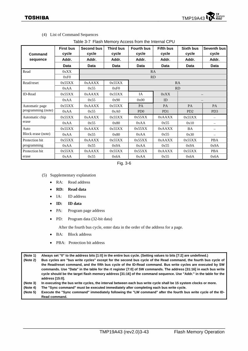
TMP19A43
TMP19A43 (rev2.0)3-43 Flash Memory Operation
(4) List of Command Sequences
Table 3-7 Flash Memory Access from the Internal CPU
First bus cycle
Second bus cycle
Third buscycle
Fourth buscycle
Fifth bus cycle
Sixth bus cycle
Seventh buscycle
Addr. Addr. Addr. Addr. Addr. Addr. Addr.
Command sequence
Data Data Data Data Data Data Data
0xXX RA Read 0xF0 RD
0x55XX 0xAAXX 0x55XX RA Read/reset 0xAA 0x55 0xF0 RD
0x55XX 0xAAXX 0x55XX IA 0xXX − ID-Read 0xAA 0x55 0x90 0x00 ID −
0x55XX 0xAAXX 0x55XX PA PA PA PA Automatic page programming (note) 0xAA 0x55 0xA0 PD0 PD1 PD2 PD3
0x55XX 0xAAXX 0x55XX 0x55XX 0xAAXX 0x55XX − Automatic chip erase 0xAA 0x55 0x80 0xAA 0x55 0x10 −
0x55XX 0xAAXX 0x55XX 0x55XX 0xAAXX BA − Auto Block erase (note) 0xAA 0x55 0x80 0xAA 0x55 0x30 −
0x55XX 0xAAXX 0x55XX 0x55XX 0xAAXX 0x55XX PBA Protection bit programming 0xAA 0x55 0x9A 0xAA 0x55 0x9A 0x9A
0x55XX 0xAAXX 0x55XX 0x55XX 0xAAXX 0x55XX PBA Protection bit erase 0xAA 0x55 0x6A 0xAA 0x55 0x6A 0x6A
Fig. 3-6
(5) Supplementary explanation
• RA: Read address
• RD: Read data
• IA: ID address
• ID: ID data
• PA: Program page address
• PD: Program data (32-bit data)
After the fourth bus cycle, enter data in the order of the address for a page.
• BA: Block address
• PBA: Protection bit address
(Note 1) Always set "0" to the address bits [1:0] in the entire bus cycle. (Setting values to bits [7:2] are undefined.) (Note 2) Bus cycles are "bus write cycles" except for the second bus cycle of the Read command, the fourth bus cycle of
the Read/reset command, and the fifth bus cycle of the ID-Read command. Bus write cycles are executed by SW commands. Use "Data" in the table for the rt register [7:0] of SW commands. The address [31:16] in each bus write cycle should be the target flash memory address [31:16] of the command sequence. Use "Addr." in the table for the address [15:0].
(Note 3) In executing the bus write cycles, the interval between each bus write cycle shall be 15 system clocks or more. (Note 4) The "Sync command" must be executed immediately after completing each bus write cycle. (Note 5) Execute the "Sync command" immediately following the "LW command" after the fourth bus write cycle of the ID-
Read command.

TMP19A43
TMP19A43 (rev2.0)3-44 Flash Memory Operation
(5) Address bit configuration for bus write cycles
Table 20.5.1.3 Address Bit Configuration for Bus Write Cycles
Address Addr
[31:21] Addr [20]
Addr [19]
Addr [18:17]
Addr[16]
Addr [15]
Addr [14]
Addr [13]
Addr [12:9]
Addr [8]
Addr [7:0]
Normal bus write cycle address configuration Normal commands
Flash area "0" is recommended Command
Addr [1:0]=0 (fixed), Others: 0 (recommended)
BA: Block address (Set the sixth bus write cycle address for block erase operation) Block erase Flash area "0" is recommended Block
selection Addr[1:0]=0 (fixed), Others: 0 (recommended)
PA: Program page address (Set the fourth bus write cycle address for page programming operation)Auto page program-ming
Flash area "0" is recommended
Block selection Page selection
Addr[1:0]=0 (fixed), Others: 0 (recommended)
IA: ID address (Set the fourth bus write cycle address for ID-Read operation) ID-READ Flash area "0" is recommended ID address Addr[1:0]=0 (fixed), Others: 0 (recommended)
PBA: Protection bit address (Set the seventh bus write cycle address for protection bit programming)Protection bit program-ming Flash area "0" is recommended
Protection bit write 00: Block 0 01: Block 1 10: Block 2 11: Block 3
Addr[1:0]=0 (fixed), Others: 0 (recommended)
PBA: Protection bit address (Set the seventh bus write cycle address for protection bit erasure)
Protection bit erase Flash area "0" is recommended
Erase protection for 0: Blocks 0, 1 1: Blocks 2, 3
Addr[1:0]=0 (fixed), Others: 0 (recommended)
(Note) Table 20.5.1.2 "Flash Memory Access from the Internal CPU" can also be used.
(Note) Address setting can be performed according to the "Normal bus write cycle address configuration" from the first bus cycle.
(Note) ""0" is recommended" can be changed as necessary.

TMP19A43
TMP19A43 (rev2.0)3-45 Flash Memory Operation
Table 3-8 Block Erase Address Table
Address Range BA
Flash Memory Address When applied to the projected area Size
Block 0 0xBFC0_0000-0xBFC1_FFFF 0x0000_0000-0x0001_FFFF 128 kB Block 1 0xBFC2_0000-0xBFC3_FFFF 0x0002_0000-0x0003_FFFF 128 kB Block 2 0xBFC4_0000-0xBFC5_FFFF 0x0004_0000-0x0005_FFFF 128 kB Block 3 0xBFC6_0000-0xBFC7_FFFF 0x0006_0000-0x0007_FFFF 128 kB
Example: When BA0 is to be selected, any single address in the range 0xBFC0_0000 to 0xBFC1_FFFF may be entered.
Table 3-9 Protection Bit Programming Address Table
The seventh bus write cycle address [15:14] OPBA
Address [15] Address [14]
Block 0 0 0 Block 1 0 1 Block 2 1 0 Block 3 1 1
Table 3-10 Protection Bit Erase Address Table
The seventh bus write cycle address [15:14] OPBA
Address [15] Address [14]
Block 0 0 X Block 1 0 X Block 2 1 X Block 3 1 X
The protection bit erase command will erase bits 0 and 1 together. The bits 2 and 3 are also erased together.
Table 3-11 The ID-Read command's fourth bus write cycle ID address (IA) and
the data to be read by the following LW command (ID)
IA [15:14] ID [7: 0] Code
00b 0x98 Manufacturer code 01b 0x5A Device code 10b Reserved --- 11b 0x05 Macro code

TMP19A43
TMP19A43 (rev2.0) 4-1 Various protecting functions
4. Various protecting functions
4.1 Overview
The ROM protect function for designating the internal ROM (flash) area as a read-protected area and the DSU
protect function for prohibiting the use of DSU (DSU-Probe) are built into the TMP19A43. The read protect
functions specifically include the following:
• Flash protect function
• ROM data protect function
• DSU protect function
4.2 Features
4.2.1 Flash Protect Function
<FLASH>
A built-in flash can prohibit the operation of writing and the deletion at every the block of every 128
Kbyte. This function is called the block protecting.
To make the block protecting function effective, it protects it corresponding to the block where it wants
to put protecting.
The bit is made "1". The block protecting can be released by making the protecting bit "0". (Please see
the chapter of the Flash operation explanation about the program method. )The protecting bit can be
monitored by FLCS register < BLPRO3:0 > bit.
The state to put protecting on all blocks is called the FLASH protecting. It is necessary to note it
because all the protecting bits become "0" after automatically deleting all data of the flash when the
protecting release operates after it puts it into the state of the LASH protecting of 1°F(operation that
makes the protecting bit "0").
<Mask>
FLASH is always being protected in the mask version, and the FLASH protecting cannot be
released. This function doesn't influence usual operation in the mask version.
<FLASH/MASK>
It is necessary to be protecting FLASH to make "ROM data protecting" and "DSU protecting" that will explain in the future effective.

TMP19A43
TMP19A43 (rev2.0) 4-2 Various protecting functions
4.2.2 ROM data Protect
As for ROM data protecting, the execution of the command to the flash is prohibited in the function it,
and the flash version that limits reading data to building FLASH/ROM into. When ROM protecting
register ROMSEC1<RSECON > bit is "1", ROM data protecting becomes effective with FLASH
protected.
If instructions in the ROM area have been replaced with instructions in the RAM area in a PC by
using the ROM correction function, a PC shows the instructions as residing in the flash ROM area.
Because they actually reside in the RAM area, data cannot be read in a ROM protected state. To read
data by using instructions held in the overwritten RAM area, it is necessary to write data to RAM by
using a program available in the ROM area or to use other means.
If the ROM area is put in a protected state, the following operations cannot be performed:
• Using instructions placed in areas other than the ROM area to load or store the data taken from
the ROM area
• Store to DMAC register (NMI by the bus error is generated. )
• Loading or storing the data taken from the ROM area in accordance with EJTAG
• Using BOOT-ROM to load or store the data taken from the ROM area (FLASH only)
• Executing flash writer to load or store the data taken from the ROM area(FLASH only)
• Using instructions placed in areas other than the ROM area to access the registers (ROMSEC1,
ROMSEC2) that concern the protection of the ROM area
• Executing the command to unprotect automatic blocking in writer mode, performing the flash
command sequences other than the automatic blocking unprotect command sequence, and
performing the flash command sequence in single or boot mode by specifying an address in
the ROM area(FLASH only)
The following operations can be performed even if the ROM area is in a protected state:
• Using instructions placed in the ROM area to load the data taken from the ROM area
• Using instructions placed in all areas to load the data taken from areas other than the ROM
area
• Using instructions placed in all areas to make instructions branch off to the ROM area
• Performing PC trace (there are restrictions) or break on the ROM area in accordance with
EJTAG
• Data transfer of ROM area by DMAC

TMP19A43
TMP19A43 (rev2.0) 4-3 Various protecting functions
4.2.3 DSU Protect
The DSU protecting function is a function for invalidating the connection of DSU-probe to enable third
parties other than the user to read the data of a built-in flash easily.
When SEQMOD register < DSUOFF > bit is "1", the DSU protecting becomes effective with FLASH
protected.
In the DSUOFF bit, the flash version, the mask version, and the state of the first stage are "1. "It enters
the state of the DSU protecting as long as the FLASH protecting is always effective in the mask version,
and the DSUOFF bit is not set to "0" by the user program.
It doesn't enter the state of the DSU protecting if protecting is not put on all blocks of FLASH in the
flash version. An initial state enters the state of the DSU protecting as well as the mask version when
FLASH is being protected putting protecting on all blocks of FLASH.
(note)
The DSUOFF bit can be accessed only with the instruction put on built-in ROM in the state of ROM
data protecting. It is necessary to note it because it is necessary to put the program of the DSU
protecting release on built-in ROM.

TMP19A43
TMP19A43 (rev2.0) 4-4 Various protecting functions
4.3 Protect Configuration and Protect Statuses
Fig. 4-1 Various Protect Statuses
Table 4-1 Protect Statuses in Each Mode
Protect bit setting FLCS<BLPRO 3:0> 1111 ≠ 1111 ROM protect enable bit ROMSEC1<RSECON> 1 0 Don't CareDSU protect enable bit SEQMOD <DSUOFF> 1 0 1 0 Don't CareFlash read protect status ON OFF ROM protect status ON OFF OFF
DSU protect status ON OFF ON OFF OFF Read of flash from internal ROM Read of flash from areas other than internal ROM × *1 × *1 Clearing of ROM protect enable status (from ROM) Clearing of ROM protect enable status (from areas other than ROM) × *2 × *2
Clearing of DSU protect enable status (from ROM) Clearing of DSU protect enable status (from areas other than ROM) × *3
Issuing of the command to erase protect bits × *4 × *4 *8 *8 Issuing of commands other than the command to erase protect bits × *5 × *5 × *7 × *7 ∆ *9
Writing of data to the DMAC setting register (from ROM)
Single /single boot mode
Writing of data to the DMAC setting register (from areas other than ROM) × *6 × *6
*1 : The data of address "0xBFC0_0000" or "0xBFC0_0002" can be read. *2 : Stored data is masked. A write to registers cannot be executed (data in registers cannot be cleared). *3 : Stored data is masked. A write to registers cannot be executed (data in registers cannot be cleared). *4 : A command address is masked, and flash memory does not recognize commands. *5 : A command address is masked, and flash memory does not recognize commands. *6 : A bus error exception occurs (when making the DMAC register setting). *7 : Because a read of flash memory is prohibited, commands are not recognized. *8 : Because a read of flash memory is prohibited, issued commands are converted to the command for erasing the whole flash
memory area and the command for erasing all protect bits.
Chip
Protect bit FLCS<BLPRO3:0>
If the bit is "1111"
ROMSEC1<RSECON>
ROM Data protect
Flash d protect function
SEQMOD <DSUOFF>
DSU protect
CS_DMAC
A bus error exception occursNMI
19A43F
During a write of data from areas other than internal ROM to the DMAC register

TMP19A43
TMP19A43 (rev2.0) 4-5 Various protecting functions
4.4 Register
Flash control/status register
This register shows the status of flash memory being monitored and the block protect status of flash memory.
Table 4-2 Flash Control Register
7 6 5 4 3 2 1 0 FLCS Bit Symbol BLPRO3 BLPRO2 BLPRO1 BLPRO0 ROMTYPE RDY/BSY (0xFFFF_E520) Read/Write R R R R R After reset
by power-on 0
(1) 0
(1) 0
(1) 0
(1) 0 0
(1) 0 1
Function Protect area setting (in units of 128 KB) 0000: All blocks unprotected xxx1: Block 0 protected xx1x: Block 1 protected x1xx: Block 2 protected 1xxx: Block 3 protected (MASK:”1111”)
"0" is read.
ROM identification bit 0: Flash 1: MROM
"0" is read.
Ready/Busy 0: In auto operation 1: Auto operation completed (MASK:”1”)
15 14 13 12 11 10 9 8 Bit Symbol Read/Write R After reset
by power-on 0 0 0 0 0 0 0 0
Function 23 22 21 20 19 18 17 16 Bit Symbol Read/Write R After reset
by power-on 0 0 0 0 0 0 0 0
Function 31 30 29 28 27 26 25 24 Bit Symbol Read/Write R After reset
by power-on 0 0 0 0 0 0 0 0
Function
Bit 0: Ready/Busy flag bit The RDY/BSY output is provided to identify the status of auto operation. This bit is a functional bit for monitoring this function by communicating with the CPU. If flash memory is in auto operation, "0" is output to show that flash memory is busy. As flash memory completes auto operation and goes into a ready state, "1" is output and the next command will be accepted. If the result of auto operation is faulty, this bit continues to output "0." It returns to "1" upon a hardware reset.
(Note) Before issuing a command, make sure that flash memory is in a ready state. If a command is issued when flash memory is busy, a right command cannot be generated and there is the possibility that subsequent commands may not be able to be input. In this case, you must return to a normal functional state by executing a system reset or issuing a reset command.
Bit 2: ROM type identification bit
This bit is used to identify the type of flash ROM or the type of mask ROM based on the value after a reset.
Flash ROM: "0" Mask ROM: "1"
Bit [7:4]: Protect bit (x: A combination setting can be made for each block) The protect bit (4-bit) value corresponds to the protect status of each block. If this bit is "1," the corresponding block is in a protected state. A protected block cannot be overwritten.
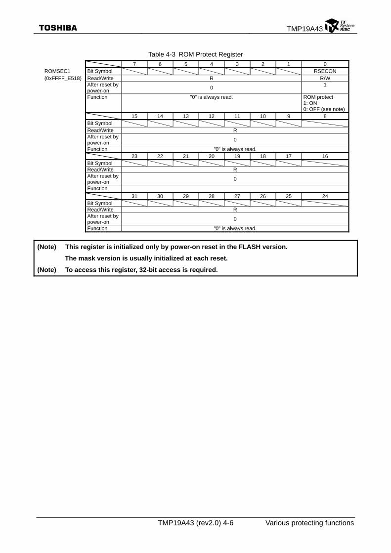
TMP19A43
TMP19A43 (rev2.0) 4-6 Various protecting functions
Table 4-3 ROM Protect Register
7 6 5 4 3 2 1 0 ROMSEC1 Bit Symbol RSECON (0xFFFF_E518) Read/Write R R/W After reset by
power-on 0
1
Function "0" is always read. ROM protect 1: ON 0: OFF (see note)
15 14 13 12 11 10 9 8 Bit Symbol
Read/Write R After reset by
power-on 0
Function "0" is always read. 23 22 21 20 19 18 17 16 Bit Symbol Read/Write R After reset by
power-on 0
Function
31 30 29 28 27 26 25 24 Bit Symbol Read/Write R After reset by
power-on 0
Function "0" is always read.
(Note) This register is initialized only by power-on reset in the FLASH version.
The mask version is usually initialized at each reset.
(Note) To access this register, 32-bit access is required.
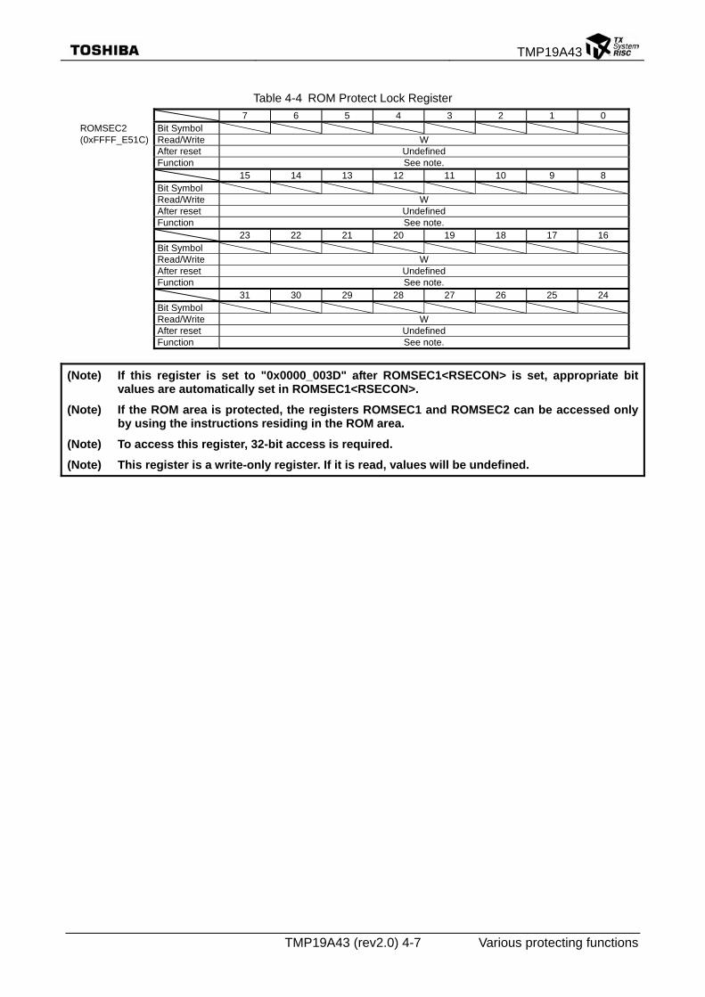
TMP19A43
TMP19A43 (rev2.0) 4-7 Various protecting functions
Table 4-4 ROM Protect Lock Register
7 6 5 4 3 2 1 0 ROMSEC2 Bit Symbol (0xFFFF_E51C) Read/Write W After reset Undefined Function See note. 15 14 13 12 11 10 9 8 Bit Symbol Read/Write W After reset Undefined Function See note. 23 22 21 20 19 18 17 16 Bit Symbol Read/Write W After reset Undefined Function See note. 31 30 29 28 27 26 25 24 Bit Symbol Read/Write W After reset Undefined Function See note.
(Note) If this register is set to "0x0000_003D" after ROMSEC1<RSECON> is set, appropriate bit values are automatically set in ROMSEC1<RSECON>.
(Note) If the ROM area is protected, the registers ROMSEC1 and ROMSEC2 can be accessed only by using the instructions residing in the ROM area.
(Note) To access this register, 32-bit access is required.
(Note) This register is a write-only register. If it is read, values will be undefined.

TMP19A43
TMP19A43 (rev2.0) 4-8 Various protecting functions
Table 4-5 DSU Protect Mode Register
7 6 5 4 3 2 1 0 SEQMOD Bit Symbol DSUOFF (0xFFFF_E510) Read/Write R R/W After reset 0 1 Function "0" is always read. 1: DSU disabled
0: DSU enabled 15 14 13 12 11 10 9 8 Bit Symbol Read/Write R After reset 0 Function "0" is always read. 23 22 21 20 19 18 17 16 Bit Symbol Read/Write R After reset 0 Function 31 30 29 28 27 26 25 24 Bit Symbol Read/Write R After reset 0 Function "0" is always read.
(Note) This register is initialized only by power-on reset in the FLASH version.
(Note) The mask version is usually initialized at each reset. To access this register, 32-bit access is required.
Table 4-6 DSU Protect Control Register
7 6 5 4 3 2 1 0 SEQCNT Bit Symbol DSECODE07 DSECODE06 DSECODE05 DSECODE04 DSECODE03 DSECODE02 DSECODE01 DSECODE00
(0xFFFF_E514) Read/Write W After reset 0 Function Write "0x0000_00C5." 15 14 13 12 11 10 9 8 Bit Symbol DSECODE15 DSECODE14 DSECODE13 DSECODE12 DSECODE11 DSECODE10 DSECODE09 DSECODE08
Read/Write W After reset 0 Function Write "0x0000_00C5." 23 22 21 20 19 18 17 16 Bit Symbol DSECODE23 DSECODE22 DSECODE21 DSECODE20 DSECODE19 DSECODE18 DSECODE17 DSECODE16
Read/Write W After reset 0 Function Write "0x0000_00C5." 31 30 29 28 27 26 25 24 Bit Symbol DSECODE31 DSECODE30 DSECODE29 DSECODE28 DSECODE27 DSECODE26 DSECODE25 DSECODE24
Read/Write W After reset 0 Function Write "0x0000_00C5."
(Note) To access this register, 32-bit access is required.
(Note) This register is a write-only register. If it is read, values will be undefined.

TMP19A43
TMP19A43 (rev2.0) 4-9 Various protecting functions
4.5 Proted-related / Release Settings
If it is necessary to overwrite flash memory or protect bits in a protected state, "automatic protect bit deletion"
must be executed or the ROM protect function must be disabled. DSU cannot be used if it is in a protected state.
Flash memory may go into a read-protected state after the automatic protect bit program is executed. In this case,
it is necessary to set DSU-PROBE to "enable" before the automatic protect bit program is executed.
(The mask version is possible only the release of ROM security, and the protecting bit cannot be rewritten.)
If "automatic protect bit deletion" is executed when flash memory is in a read-protected state, flash memory is
automatically initialized inside this device. Therefore, extra caution must be used when switching from one state
to a read-protected state. (FLASH only)
4.5.1 Flash Protect Function
The flash protecting function cannot be released always effectively in the mask version.
It becomes effective by putting the block protecting on all of the four blocks in the flash version.
The flash memory command sequence and protect bit program commands are used to enable or
disable the flash read protect function. For further information, refer to the command sequence
explained in the chapter describing the operations of flash memory.
(notes concerning FLASH version)
The protecting bit is cleared after all the data of the flash is deleted when the protecting bit release
command is executed with the flash protected, and the flash protecting is released.
In the state of ROM data protecting, explains as follows, the command execution to the flash is
disregarded. It is necessary to release ROM data protecting first clearing the RSECON bit of ROM
protecting register when the flash protecting is released with ROM protected.
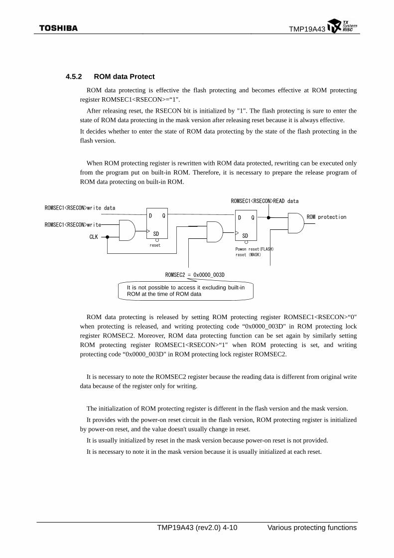
TMP19A43
TMP19A43 (rev2.0) 4-10 Various protecting functions
4.5.2 ROM data Protect
ROM data protecting is effective the flash protecting and becomes effective at ROM protecting
register ROMSEC1<RSECON>=“1".
After releasing reset, the RSECON bit is initialized by "1". The flash protecting is sure to enter the
state of ROM data protecting in the mask version after releasing reset because it is always effective.
It decides whether to enter the state of ROM data protecting by the state of the flash protecting in the
flash version.
When ROM protecting register is rewritten with ROM data protected, rewriting can be executed only
from the program put on built-in ROM. Therefore, it is necessary to prepare the release program of
ROM data protecting on built-in ROM.
ROM data protecting is released by setting ROM protecting register ROMSEC1<RSECON>“0"
when protecting is released, and writing protecting code “0x0000_003D" in ROM protecting lock
register ROMSEC2. Moreover, ROM data protecting function can be set again by similarly setting
ROM protecting register ROMSEC1<RSECON>“1" when ROM protecting is set, and writing
protecting code “0x0000_003D" in ROM protecting lock register ROMSEC2.
It is necessary to note the ROMSEC2 register because the reading data is different from original write
data because of the register only for writing.
The initialization of ROM protecting register is different in the flash version and the mask version.
It provides with the power-on reset circuit in the flash version, ROM protecting register is initialized
by power-on reset, and the value doesn't usually change in reset.
It is usually initialized by reset in the mask version because power-on reset is not provided.
It is necessary to note it in the mask version because it is usually initialized at each reset.
ROMSEC1<RSECON>write
ROMSEC1<RSECON>write data
CLK
reset
ROM protection
ROMSEC1<RSECON>READ data
ROMSEC2 = 0x0000_003D
It is not possible to access it excluding built-in ROM at the time of ROM data
D Q
SD
D Q
SD
Powon reset(FLASH)
reset(MASK)

TMP19A43
TMP19A43 (rev2.0) 4-11 Various protecting functions
4.5.3 DSU Protect
DSU data protecting is effective the flash protecting and becomes effective at DSU protecting register
SEQMOD<RSECON>=“1".
After releasing reset, the DSUOFF bit is initialized by "1". The flash protecting is sure to enter the
state of DSU data protecting in the mask version after releasing reset because it is always effective.
It decides whether to enter the state of ROM data protecting by the state of the flash protecting in the
flash version.
When DSU protecting register is rewritten with ROM data protected, rewriting can be executed only
from the program put on built-in ROM. Therefore, it is necessary to prepare the release program of
DSU data protecting on built-in ROM.
DSU protecting is released by setting DSU protecting register SEQMOD<DSUOFF>“0" when
protecting is released, and writing protecting code “0x0000_00C5" in ROM protecting lock register
SEQCNT. Moreover, DSU protecting function can be set again by similarly setting ROM protecting
register SEQMOD<DSUOFF>“1" when DSU protecting is set, and writing protecting code
“0x0000_00C5" in DSU protecting lock register SEQCNT.
It is necessary to note the SEQCNT register because the reading data is different from original write
data because of the register only for writing.
The initialization of DSU protecting register is different in the flash version and the mask version.
It provides with the power-on reset circuit in the flash version, DSU protecting register is initialized
by power-on reset, and the value doesn't usually change in reset.
It is usually initialized by reset in the mask version because power-on reset is not provided.
It is necessary to note it in the mask version because it is usually initialized at each reset.
SEQMOD<DSUOFF>write
SEQMOD<DSUOFF>write data
CLK
reset
DSU protection
SEQMOD<DSUOFF>READ data
SEQCNT = 0x0000_00C5
It is not possible to access it excluding built-in ROM at the time of ROM data
D Q
SD
D Q
SD
Powon reset(FLASH)
reset(MASK)
FLASH protection

TMP19A43
TMP19A43 (rev2.0) 4-12 Various protecting functions
4.5.4 ROM Protect Register: ROMSEC1<RSECON>
The ROM protect register is equipped with a power-on reset circuit. Caution must be exercised as data
read from the ROMSEC1<RSECON> bit is different from the actually written data. How data is
processed is shown below. The mask version is usually initialized by reset though FLASH goods are
initialized by power-on reset.
4.5.5 DSU Protect Mode Register: SEQMOD <DSUOFF>
The DSU protect mode register is equipped with a power-on reset circuit. Caution must be exercised as
data read from the SEQMOD <DSUOFF> bit is different from the actually written data. How data is
processed is shown below. The mask version is usually initialized by reset though FLASH goods are
initialized by power-on reset.
SEQMOD<DSUOFF> write
Write data to SEQMOD<DSUOFF>
CLK
Reset Power-on reset
DSU protect
Flash read protect function
Read data from SEQMOD<DSUOFF>
DSUSEC2 = 0x0000_00C5
If the ROM is in a protected state, access from areas other than the internal ROM is disabled.
D Q
SD
D Q
SD
ROMSEC1<RSECON> write
Write data to ROMSEC1<RSECON>
CLK
Reset Power-on reset
ROM protect
Flash read protect function
Read data from ROMSEC1<RSECON>
ROMSEC2 = 0x0000_003D
If the ROM is in a protected state, access from areas other than the internal ROM is disabled.
D Q
SD
D Q
SD
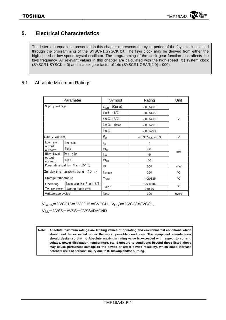
TMP19A43
TMP19A43 5-1
5. Electrical Characteristics
5.1 Absolute Maximum Ratings
Parameter Symbol Rating Unit
VCC15 (Core) − 0.3to3.0
Vcc3 (I/O) − 0.3to3.9
AVCC3(A/D) − 0.3to3.9
DAVCC (D/A) − 0.3to3.5
Supply voltage
DVCC3 − 0.3to3.9
V
Supply voltage VIN − 0.3toVCC + 0.3 V
Per pin IOL 5 Low-level
output
current Total ΣIOL 50
Per pin IOH -5 High-level
output
current Total ΣIOH 50
mA
Power dissipation (Ta = 85°C) PD 600 mW
Soldering temperature (10 s) TSOLDER 260 °C
Storage temperature TSTG −40to125 °C
Exceptduring Flash W/E -20 to 85 Operating
Temperature During Flash W/E
TOPR 0 to 70
°C
Write/erase cycles NEW 100 cycle
VCC15=DVCC15=CVCC15=CVCCH、VCC3=DVCC3=CVCCL、
VSS=DVSS=AVSS=CVSS=DAGND
The letter x in equations presented in this chapter represents the cycle period of the fsys clock selected through the programming of the SYSCR1.SYSCK bit. The fsys clock may be derived from either the high-speed or low-speed crystal oscillator. The programming of the clock gear function also affects the fsys frequency. All relevant values in this chapter are calculated with the high-speed (fc) system clock (SYSCR1.SYSCK = 0) and a clock gear factor of 1/fc (SYSCR1.GEAR[2:0] = 000).
Note: Absolute maximum ratings are limiting values of operating and environmental conditions which should not be exceeded under the worst possible conditions. The equipment manufacturer should design so that no Absolute maximum rating value is exceeded with respect to current, voltage, power dissipation, temperature, etc. Exposure to conditions beyond those listed above may cause permanent damage to the device or affect device reliability, which could increase potential risks of personal injury due to IC blowup and/or burning.
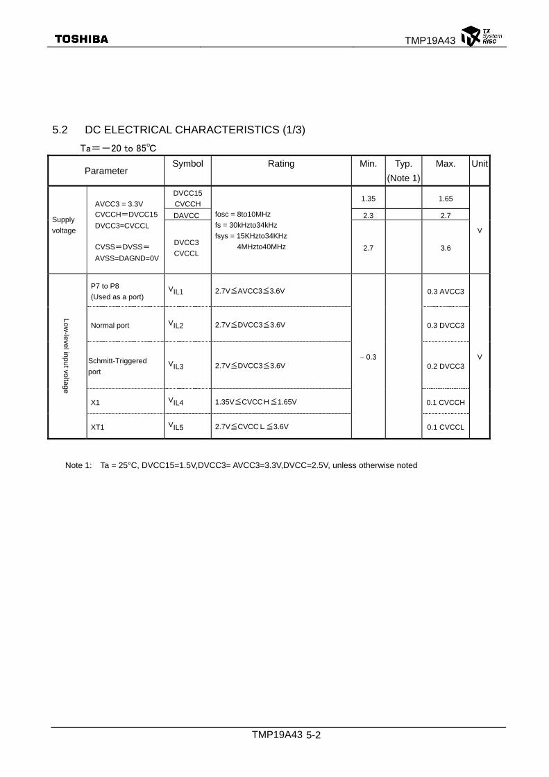
TMP19A43
TMP19A43 5-2
5.2 DC ELECTRICAL CHARACTERISTICS (1/3)
Ta=-20 to 85℃
Parameter Symbol Rating Min. Typ.
(Note 1)
Max. Unit
DVCC15
CVCCH 1.35 1.65
DAVCC 2.3 2.7 Supply
voltage
AVCC3 = 3.3V
CVCCH=DVCC15
DVCC3=CVCCL
CVSS=DVSS=
AVSS=DAGND=0V
DVCC3
CVCCL
fosc = 8to10MHz
fs = 30kHzto34kHz
fsys = 15KHzto34KHz
4MHzto40MHz 2.7 3.6
V
P7 to P8
(Used as a port) VIL1 2.7V≦AVCC3≦3.6V 0.3 AVCC3
Normal port VIL2 2.7V≦DVCC3≦3.6V 0.3 DVCC3
Schmitt-Triggered
port VIL3 2.7V≦DVCC3≦3.6V 0.2 DVCC3
X1 VIL4 1.35V≦CVCCH≦1.65V 0.1 CVCCH
Low-level input voltage
XT1 VIL5 2.7V≦CVCCL≦3.6V
− 0.3
0.1 CVCCL
V
Note 1: Ta = 25°C, DVCC15=1.5V,DVCC3= AVCC3=3.3V,DVCC=2.5V, unless otherwise noted
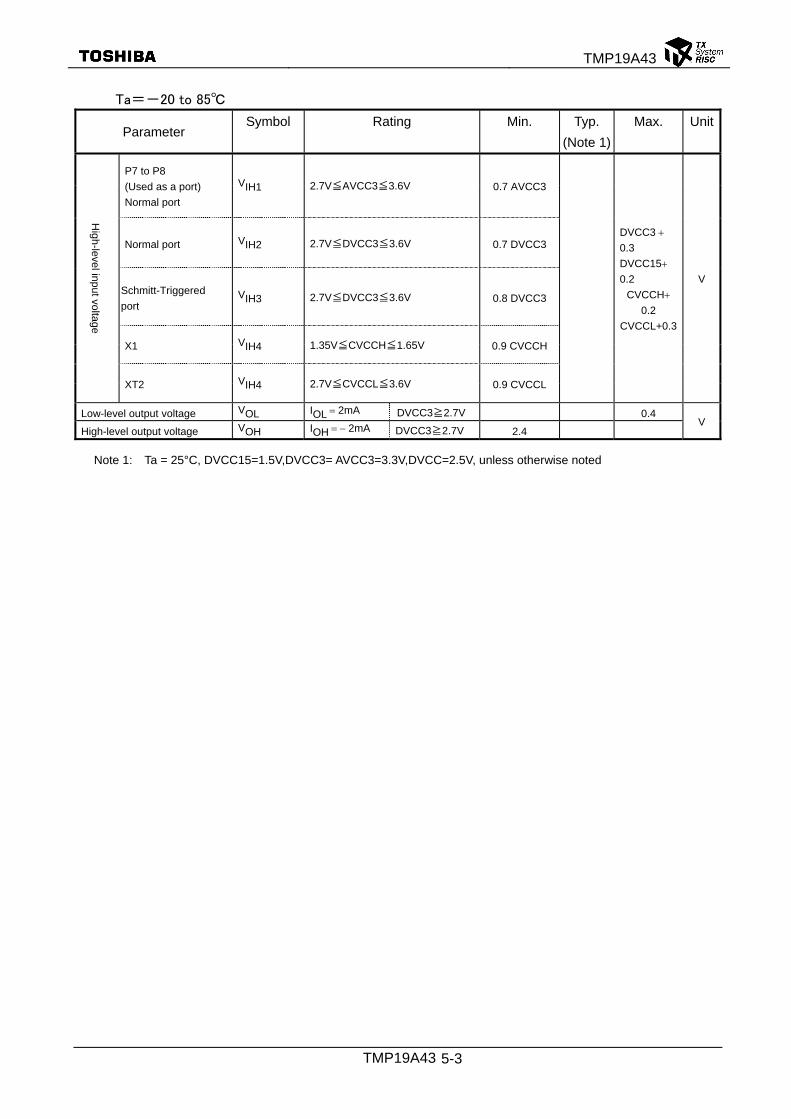
TMP19A43
TMP19A43 5-3
Ta=-20 to 85℃
Parameter Symbol Rating Min. Typ.
(Note 1)
Max. Unit
P7 to P8
(Used as a port)
Normal port
VIH1 2.7V≦AVCC3≦3.6V 0.7 AVCC3
Normal port VIH2 2.7V≦DVCC3≦3.6V 0.7 DVCC3
Schmitt-Triggered
port VIH3 2.7V≦DVCC3≦3.6V 0.8 DVCC3
X1 VIH4 1.35V≦CVCCH≦1.65V 0.9 CVCCH
High-level input voltage
XT2 VIH4 2.7V≦CVCCL≦3.6V 0.9 CVCCL
DVCC3 +
0.3
DVCC15+
0.2
CVCCH+
0.2
CVCCL+0.3
V
Low-level output voltage VOL IOL = 2mA DVCC3≧2.7V 0.4
High-level output voltage VOH IOH = − 2mA DVCC3≧2.7V 2.4 V
Note 1: Ta = 25°C, DVCC15=1.5V,DVCC3= AVCC3=3.3V,DVCC=2.5V, unless otherwise noted
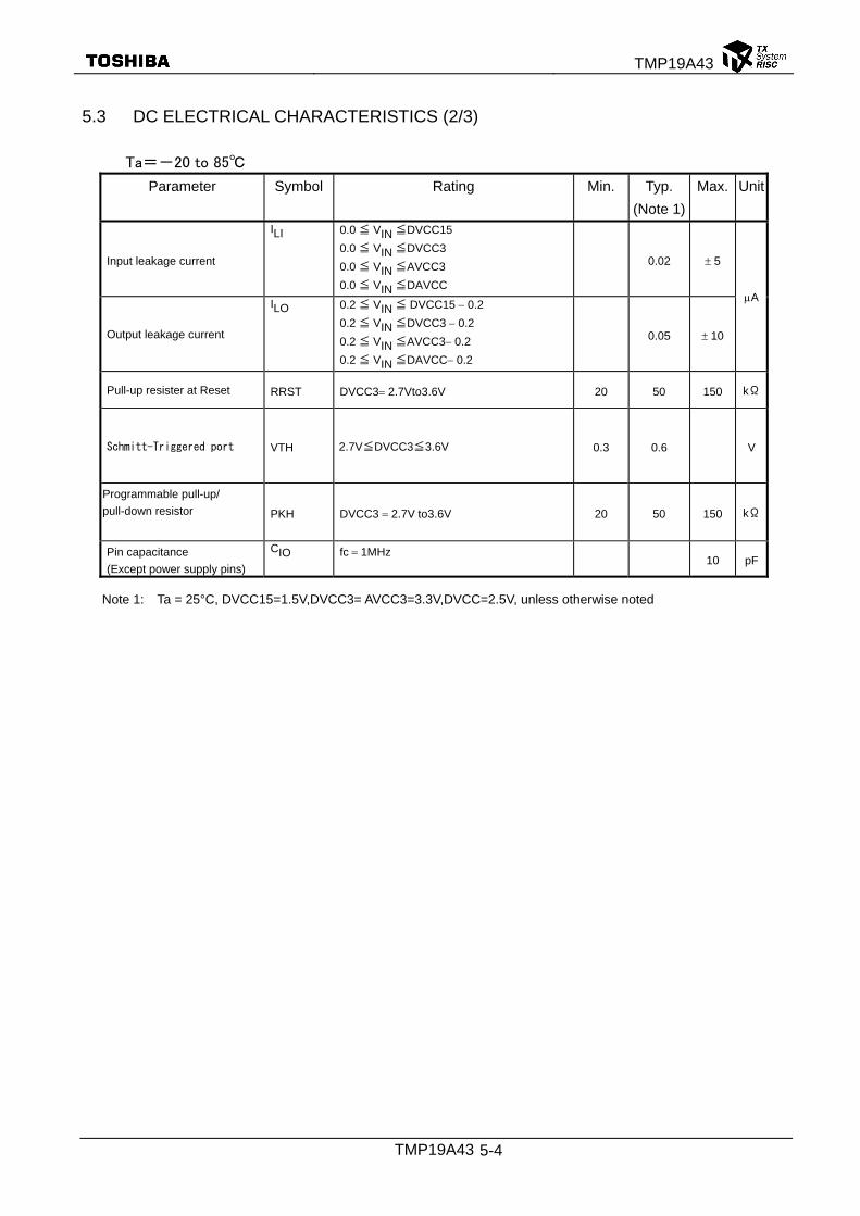
TMP19A43
TMP19A43 5-4
5.3 DC ELECTRICAL CHARACTERISTICS (2/3)
Ta=-20 to 85℃
Parameter Symbol Rating Min. Typ.
(Note 1)
Max. Unit
Input leakage current
ILI 0.0 ≦ VIN ≦DVCC15
0.0 ≦ VIN ≦DVCC3
0.0 ≦ VIN ≦AVCC3
0.0 ≦ VIN ≦DAVCC
0.02 ± 5
Output leakage current
ILO 0.2 ≦ VIN ≦ DVCC15 − 0.2
0.2 ≦ VIN ≦DVCC3 − 0.2
0.2 ≦ VIN ≦AVCC3− 0.2
0.2 ≦ VIN ≦DAVCC− 0.2
0.05 ± 10
µA
Pull-up resister at Reset RRST DVCC3= 2.7Vto3.6V 20 50 150 kΩ
Schmitt-Triggered port VTH 2.7V≦DVCC3≦3.6V 0.3 0.6 V
Programmable pull-up/
pull-down resistor PKH DVCC3 = 2.7V to3.6V 20 50 150 kΩ
Pin capacitance
(Except power supply pins)
CIO fc = 1MHz 10 pF
Note 1: Ta = 25°C, DVCC15=1.5V,DVCC3= AVCC3=3.3V,DVCC=2.5V, unless otherwise noted

TMP19A43
TMP19A43 5-5
5.4 DC ELECTRICAL CHARACTERISTICS (3/3)
DVCC15=CVCCH=1.35Vto1.65V, CVCCL= DVCC3=AVCC3=2.7Vto3.6V, DAVCC=2.3Vto2.7V
Ta=-20 to 85℃
Parameter Symbol Rating Min. Typ.
(Note 1)
Max. Unit
NORMAL(Note 2): Gear = 1/1 50 74
IDLE(Doze) (Note 3) 20 29
IDLE(Halt) (Note 3)
fsys =40 MHz
( fOSC = 10 MHz)
18 28
mA
SLOW (Note 4) fs = 32.768kHz 140 995 µA
SLEEP (Note 4) fs = 32.768kHz 30 985 µA
STOP
ICC
27 980 µA
Note 1: Ta = 25°C, DVCC15=1.5V,DVCC3= AVCC3=3.3V,DVCC=2.5V, unless otherwise noted
(note1) ICC NORMAL:
Measured with the CPU dhrystone operating ( DSU is excluded.), RAM, FLASH.
All functions operating. D/A and A/D excluded.
(note2) ICC IDLE :
Measured with all functions stoping.
(note3) ICC SLOW,SLEEP :
Measured with RTC on low-speed
ICC :The current where flows is included.
(DVCC15、DVCC3、CVCCH、CVCCL、AVCC3、DAVCC)

TMP19A43
TMP19A43 5-6
5.5 10-bit ADC Electrical Characteristics
DVCC15=CVCCH=1.35Vto1.65V, CVCCL= DVCC3=AVCC3=VREFH=2.7Vto3.6V, DAVCC=2.3Vto2.7V,AVSS = DVSS ,Ta=-20 to 85℃ AVCC3 load capacitanc= 3.3µF, VREFH load capacitanc= 3.3µF
Parameter Symbol Rating Min Typ Max Unit
Analog reference voltage ( + ) VREFH 2.7 3.3 3.6 V
Analog reference voltage ( − ) VREFL AVSS AVSS AVSS V
Analog input voltage VAIN VREFL VREFH V
A/D conversion DVSS = AVSS = VREFL 4.5 5.5 mA Analog supply
current Non-A/D
conversion
IREF
DVSS = AVSS = VREFL ± 0.02 ± 5 µA
supply current A/D conversion ⎯ Non-IREF 3 mA
INL error ± 2 ± 3
DNL error ± 1 ± 2
Offset error ± 2 ± 4
Fullscale error
⎯
AIN resistance ≦600Ω
AIN load capacitance≦30pF
Conversion time≧1.15μs
± 2 ± 4
INL error ± 2 ± 3
DNL error ± 1 ± 2
Offset error ± 2 ± 4
Fullscale error
⎯
AIN resistance ≦600Ω
AIN load capacitance≧0.1μF
Conversion time≧1.15μs
± 2 ± 4
INL error ± 2 ± 3
DNL error ± 1 ± 2
Offset error ± 2 ± 4
Fullscale error
⎯
AIN resistance ≦1.3kΩ
AIN load capacitance≧0.1μF
Conversion time≧1.15μs
± 2 ± 4
INL error ± 2 ± 3
DNL error ± 1 ± 2
Offset error ± 2 ± 4
Fullscale error
⎯
AIN resistance ≦10kΩ
AIN load capacitance≧0.1μF
Conversion time≧2.30μs
± 2 ± 4
LSB
(Note 1) 1LSB = (VREFH − VREFL) / 1024[V]
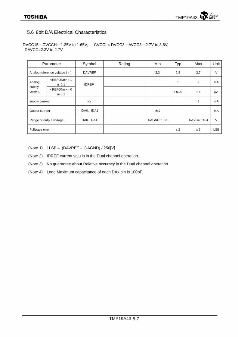
TMP19A43
TMP19A43 5-7
5.6 8bit D/A Electrical Characteristics
DVCC15=CVCCH=1.35V to 1.65V, CVCCL= DVCC3=AVCC3=2.7V to 3.6V, DAVCC=2.3V to 2.7V
Parameter Symbol Rating Min Typ Max Unit
Analog reference voltage ( + ) DAVREF
2.3 2.5 2.7 V
<REFONn> = 1
n=0,1 1 2 mAAnalog
supply
current <REFONn> = 0
n=0,1
IDREF
± 0.02 ± 5 µA
supply current Icc
5 mA
Output current IDA0,IDA1
±1 mA
Range of output voltage DA0,DA1
DAGND+0.3 DAVCC-0.3 V
Fullscale error ⎯
± 2 ± 3 LSB
(Note 1) 1LSB = (DAVREF − DAGND) / 256[V]
(Note 2) IDREF current valu is in the Dual channel operation .
(Note 3) No guarantee about Relative accuracy in the Dual channel operation
(Note 4) Load Maximum capacitance of each DAx pin is 100pF.

TMP19A43
TMP19A43 5-8
5.7 AC Electrical Characteristics
5.7.1 Multiplex Bus mode
(1) DVCC15=CVCC15=1.35Vto1.65V, AVCC3= 2.7Vto3.6V
DVCC3= 2.7Vto3.6V, DAVCC = 2.3Vto2.7V,Ta =-20to85°C
① ALE width = 1 clock cycle, 2 programmed wait state
Equation 40 MHz (fsys)(Note) No. Parameter Symbol
Min Max Min Max
Unit
1 System clock period (x) tSYS 25 ns
2 A0-A15 VALID TO ALE LOW tAL x –11 14.0 ns
3 A0-A15 HOLD AFTER ALE LOW tLA x – 8 17.0 ns
4 ALE pulse width high tLL x – 6 19.0 ns
5 ALE low to RD , WR or HWR asserted
tLC x – 8 17.0 ns
6 RD , WR or HWR negated to ALE
high
tCL x − 8 17.0 ns
7 A0-A15 valid to RD , WR or HWR
asserted
tACL 2x − 11 39.0 ns
8 A16-A23 valid to RD , WR or HWR
asserted
tACH 2x − 11 39.0 ns
9 A16-A23 hold after RD , WR or
HWR negated
tCAR x − 11
14.0 ns
10 A0-A15 valid to D0-D15 Data in tADL x (2 + TW+ALE) − 43 82.0 ns
11 A16-A23 valid to D0-D15 Data in tADH x (2 + TW+ALE) − 43 82.0 ns
12 RD asserted to D0-D15 data in tRD x (1 + TW) −40 35.0 ns
13 RD width low tRR x (1 + TW) −6 69 ns
14 D0-D15 hold after RD negated tHR 0 0 ns
15 RD negated to next A0-A15 output tRAE x− 6 19.0 ns
16 WR / HWR width low tWW x (1 + TW) − 6 69.0 ns
17 D0-D15 valid to WR or HWR negated
tDW x (1 + TW) − 11 64.0 ns
18 D0-D15 hold after WR or HWR negated
tWD x − 11 14.0 ns
19 A16-A23 valid to WAIT input tAWH x+ x (ALE)+x(TW-
1)-32 43.0 ns
20 A0-A15 valid to WAIT input tAWL x+ x (ALE)+x(TW-
1)-32 43.0 ns
21 WAIT hold after RD , WR or HWR
asserted
tCW x(TW - 3)-16 x(TW – 1) – 29 9.0 46.0 ns
Note 1: No. 1 to 21:
Internal 2 wait insertion ,ALE “1” Clock,@40MHz
TW = W + 2N ,
W : Number of Auto wait insertion , 2N : Number of external wait insertion
TW = 2 + 2*1 = 4
AC measurement conditions:
Output levels: High = 0.8DVCC3 V/Low 0.2DVCC3 V, CL = 30 pF
Input levels: High = 0.7DVCC3 V/Low 0.3DVCC3 V

TMP19A43
TMP19A43 5-9
② ALE width = 1 clock cycles, 2 programmed wait state
Equation 40 MHz (fsys)(Note) No. Parameter
Symbol
Min Max Min Max
Unit
1 System clock period (x) tSYS 25 ns
2 A0-A15 VALID TO ALE LOW tAL x –11 14.0 ns
3 A0-A15 HOLD AFTER ALE LOW tLA x – 8 17.0 ns
4 ALE pulse width high tLL x – 6 19.0 ns
5 ALE low to RD , WR or HWR asserted
tLC x – 8 17.0 ns
6 RD , WR or HWR negated to ALE
high
tCL x − 8 17.0 ns
7 A0-A15 valid to RD , WR or HWR
asserted
tACL 2x − 11 39.0 ns
8 A16-A23 valid to RD , WR or HWR
asserted
tACH 2x − 11 39.0 ns
9 A16-A23 hold after RD , WR or
HWR negated
tCAR x − 11
14.0 ns
10 A0-A15 valid to D0-D15 Data in tADL x (2 + TW+ALE) − 43 82.0 ns
11 A16-A23 valid to D0-D15 Data in tADH x (2 + TW+ALE) − 43 82.0 ns
12 RD asserted to D0-D15 data in tRD x (1 + TW) −40 35.0 ns
13 RD width low tRR x (1 + TW) −6 69 ns
14 D0-D15 hold after RD negated tHR 0 0 ns
15 RD negated to next A0-A15 output tRAE x− 6 19.0 ns
16 WR / HWR width low tWW x (1 + TW) − 6 69.0 ns
17 D0-D15 valid to WR or HWR negated
tDW x (1 + TW) − 11 64.0 ns
18 D0-D15 hold after WR or HWR negated
tWD x − 11 14.0 ns
19 A16-A23 valid to WAIT input tAWH x+ x (ALE)+x(TW-
1)-32 43.0 ns
20 A0-A15 valid to WAIT input tAWL x+ x (ALE)+x(TW-
1)-32 43.0 ns
21 WAIT hold after RD , WR or HWR
asserted
tCW x(TW - 3)-16 x(TW – 1) – 29 9.0 46.0 ns
Note 1: No. 1 to 21:
Internal 2 wait insertion ,ALE “1” Clock,@40MHz
TW = W + 2N ,
W : Number of Auto wait insertion , 2N : Number of external wait insertion
TW = 2 + 2*1 = 4
AC measurement conditions:
Output levels: High = 0.8DVCC3 V/Low 0.2DVCC3 V, CL = 30 pF
Input levels: High = 0.7DVCC3 V/Low 0.3DVCC3 V

TMP19A43
TMP19A43 5-10
(1) Read cycle timing, ALE width = 1 clock cycle, 1 programmed wait state
tCAR tRR
tHR tADH
tADL
tLA
D0∼15
tAL tCL
tLL
ALE
InternalCLK
AD0~15
RD
A0∼15
tACL tACH
tLC
tRD
A16~23
5CLK/1BUS Cycle
S1i S2 S3 S1 W1
tRAE
CS0~3
R/W
S1 S2 S0 S1iSw

TMP19A43
TMP19A43 5-11
(2) Read cycle timing, ALE width = 1 clock cycle, 2 programmed wait state
tCARtRR
tHR tADH
tADL
tLA
D0∼15
tAL tCL
tLL
ALE
InternalCLK
AD0~15
RD
A0∼15
tACL tACH
tLC
tRD
A16~23
6CLK/1BUS Cycle
tRAE
CS0~3
R/W

TMP19A43
TMP19A43 5-12
(3) Read cycle timing, ALE width = 1 clock cycle, 4 programmed wait state
tAWL/H
ALE
InternalCLK
AD0~15
RD
AD16~23
8CLK/1BUS Cycle
WAIT
D0∼15 A0∼15
tCW
CS0~3
R/W

TMP19A43
TMP19A43 5-13
(4) Read cycle timing, ALE width = 2 clock cycle, 1 programmed wait state
tRR
tHR tADH
tADL
tLA
D0∼15
tAL tCL
tLL
ALE
InternalCLK
AD0~15
RD
S1i S1x Sw S2 S0
A0∼15
tACL tACH
tLC
tRD
A16~23
6CLK/1BUS Cycle
S1
tRAE
CS0~3
R/W
S1i
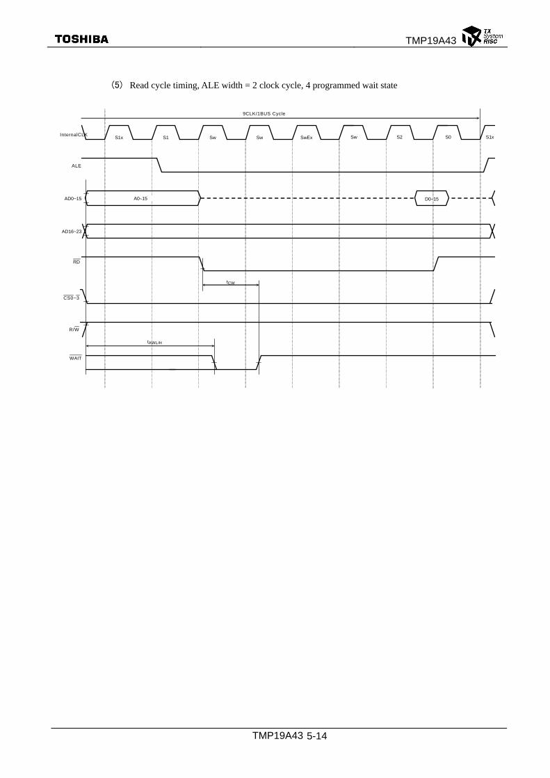
TMP19A43
TMP19A43 5-14
(5) Read cycle timing, ALE width = 2 clock cycle, 4 programmed wait state
tAWL/H
ALE
InternalCLK
AD0~15
RD
AD16~23
9CLK/1BUS Cycle
WAIT
D0∼15
S1x S1 Sw SwEx S0
A0∼15
Sw
tCW
CS0~3
R/W
Sw S2 S1x

TMP19A43
TMP19A43 5-15
(6) Write cycle timing, ALE width = 2 clock cycles, zero wait state
tWW tCAR
tDW
tLA
D0∼15
tAL tCL
tLL
ALE
InternalCLK
AD0~15
WR, HWR
CS0~3
R/W
A0∼15
tACL tACH
tLC
AD16~23
5CLK/1BUS Cycle
tWD
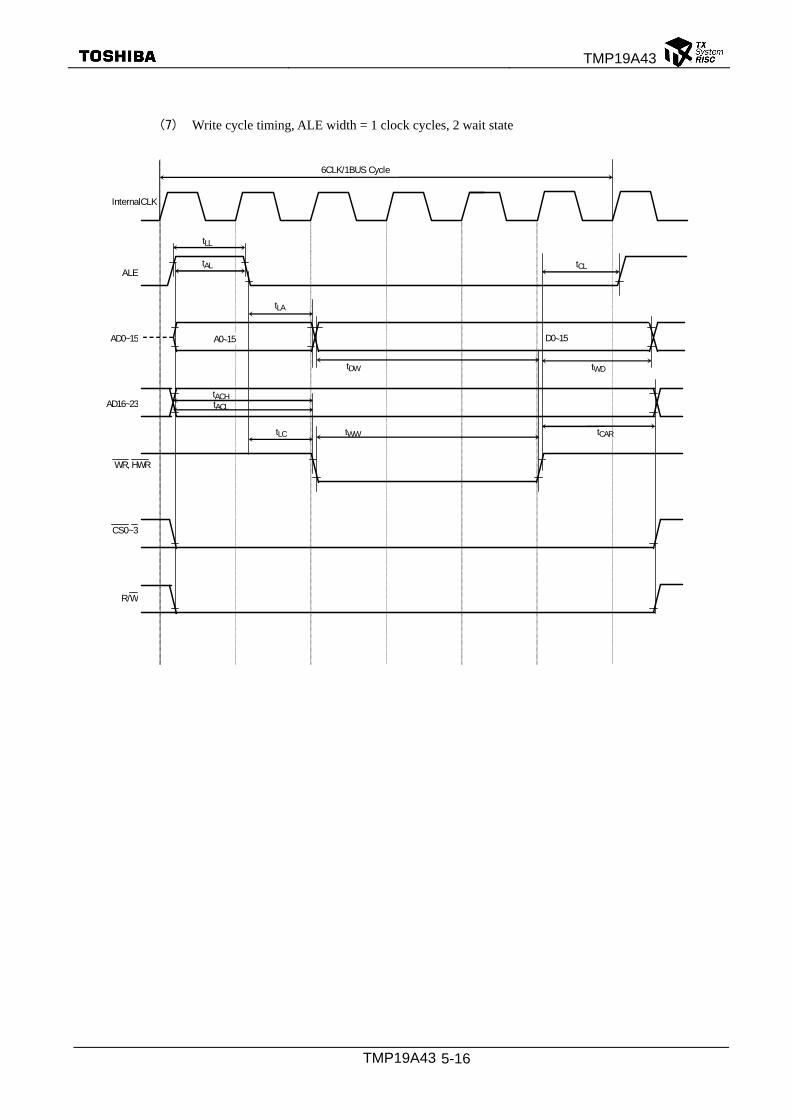
TMP19A43
TMP19A43 5-16
(7) Write cycle timing, ALE width = 1 clock cycles, 2 wait state
tWW tCAR
tDW
tLA
D0∼15
tAL tCL
tLL
ALE
InternalCLK
AD0~15
WR, HWR
CS0~3
R/W
A0∼15
tACL tACH
tLC
AD16~23
6CLK/1BUS Cycle
tWD

TMP19A43
TMP19A43 5-17
(8) Write cycle timing, ALE width = 2 clock cycles, 4 wait state
ALE
InternalCLK
AD0~15
WR, HWR
CS0~3
R/W
AD16~23
9CLK/1BUS Cycle
tWW tCAR
tDW
tLA
D0∼15
tAL tCL
tLL
A0∼15
tACL tACH
tLC
tWD
WAIT
tCW
tAWL/H

TMP19A43
TMP19A43 5-18
5.7.2 Separate Bus mode
(1) DVCC15=CVCCH=1.35Vto1.65V, DVCC3=AVCC3=2.7Vto3.6V,
DAVCC =2.3 Vto2.7V, Ta = -20 to 85°C
① SYSCR3<ALESEL> = “0”, 2 programmed wait state
Equation 40 MHz (fsys)(Note) No. Parameter
Symbol
Min Max Min Max
Unit
1 System clock period (x) tSYS 25 ns
2 A0-A23 valid to RD , WR or HWR
asserted
tAC X(1+ALE) −11 39.0 ns
3 A0-A23 hold after RD , WR or HWR
negated
tCAR x − 11 14.0 ns
4 A0-A23 valid to D0-D15 Data in tAD x (2 + TW+ALE) − 43 82.0 ns
5 RD asserted to D0-D15 data in tRD x (1 + TW) − 40 35.0 ns
6 RD width low tRR x (1 +TW) –6 69.0 ns
7 D0-D15 hold after RD negated tHR 0 0 ns
8 RD negated to next A0-A23 output tRAE x − 6 19.0 ns
9 WR /HWR width low tWW x (1 + TW) –6 69.0 ns
10 WR or HWR asserted to D0-D15 valid tDO 9.7 9.7 ns
11 D0-D15 hold after WR or HWR
negated
tDW x (1 + TW) − 11 64.0 ns
12 D0-D15 hold after WR or HWR
negated
tWD x − 11 14.0 ns
13 A0-A23 valid to WAIT input tAW x+ x (ALE)+x(TW-
1)-32 43.0 ns
14 WAIT hold after RD , WR or HWR
asserted
tCW x(TW - 3)-16 x(TW – 1) – 29 9.0 46.0 ns
Note 1: No. 1 to 14:
Internal 2 wait insertion ,ALE “1” Clock,@40MHz
TW = W + 2N ,
W : Number of Auto wait insertion , 2N : Number of external wait insertion
TW = 2 + 2*1 = 4
AC measurement conditions:
Output levels: High = 0.8DVCC3 V/Low 0.2DVCC3 V, CL = 30 pF
Input levels: High = 0.7DVCC3 V/Low 0.3DVCC3 V
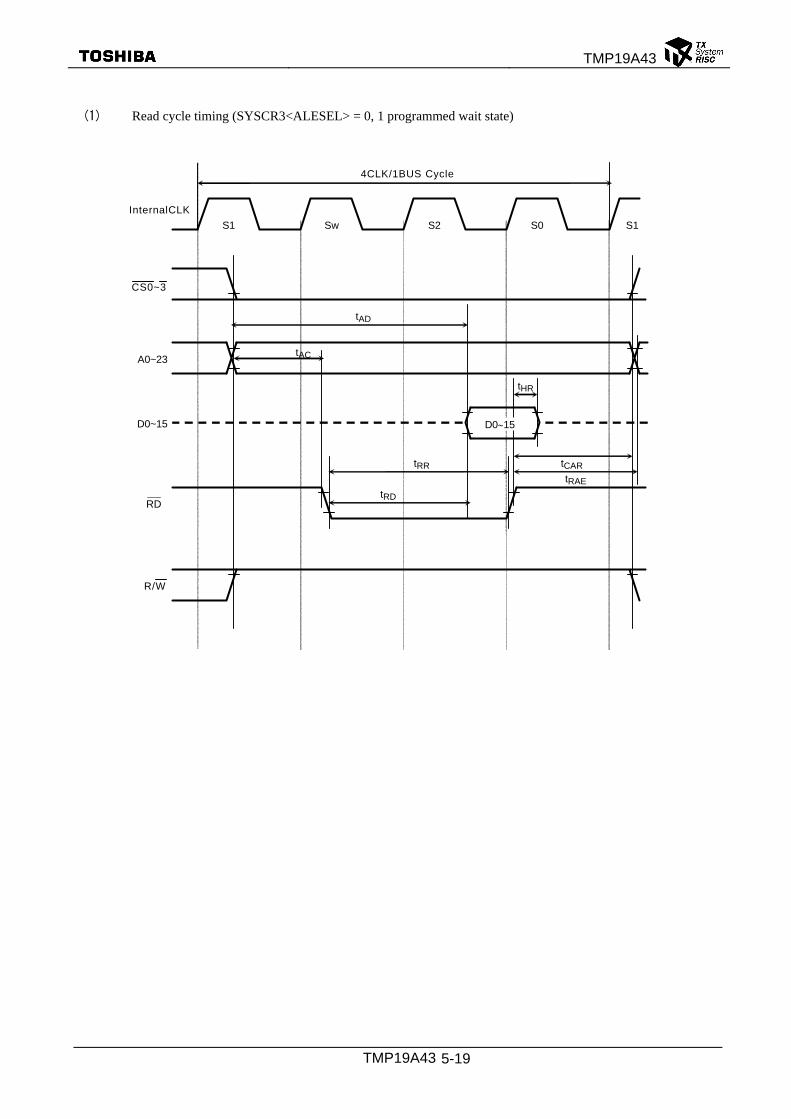
TMP19A43
TMP19A43 5-19
(1) Read cycle timing (SYSCR3<ALESEL> = 0, 1 programmed wait state)
tCAR tRR
tHR
tAD
InternalCLK
RD
tAC
tRD
A0~23
4CLK/1BUS Cycle
S1 S2 S0 S1 Sw
D0∼15D0~15
tRAE
CS0~3
R/W

TMP19A43
TMP19A43 5-20
(2) Read cycle timing (SYSCR3<ALESEL> = 1, 1 programmed wait state)
tCAR tRR
tHR tAD
tAD
InternalCLK
RD
S1i S1 S2 S0 S1i
D0∼15 D0~15
tAC
tRD
A16~23
5CLK/1BUS Cycle
Sw
tRAE
CS0~3
R/W

TMP19A43
TMP19A43 5-21
(3)Read cycle timing SYSCR3<ALESEL> = 1, 4 externally generated wait states with N = 1)
tAW
InternalCLK
RD
A0~23
8CLK/1BUS Cycle
WAIT
D0~15 D0∼15
S1 Sw SwE Sw S2 Sw
tCW
CS0~3
R/W
S1iS0

TMP19A43
TMP19A43 5-22
(4) Write cycle timing (SYSCR3<ALESEL> = 1, zero wait sate)
tWW tCAR
tDW
InternalCLK
WR, HWR
CS0~3
R/W
tAC A0~23
4CLK/1BUS Cycle
tWD
D0∼15D0~15
tDO
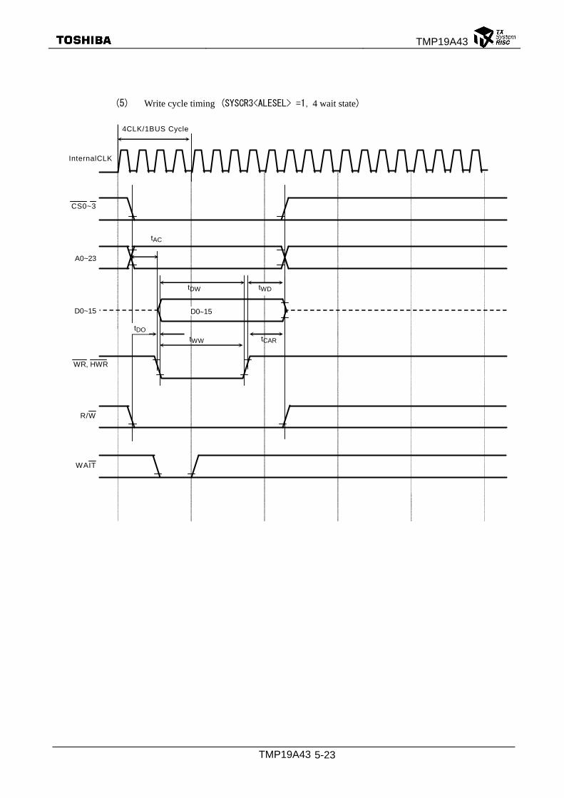
TMP19A43
TMP19A43 5-23
(5) Write cycle timing (SYSCR3<ALESEL> =1, 4 wait state)
tWW tCAR
tDW
InternalCLK
WR, HWR
CS0~3
R/W
tAC
A0~23
4CLK/1BUS Cycle
tWD
D0∼15 D0~15
tDO
WAIT
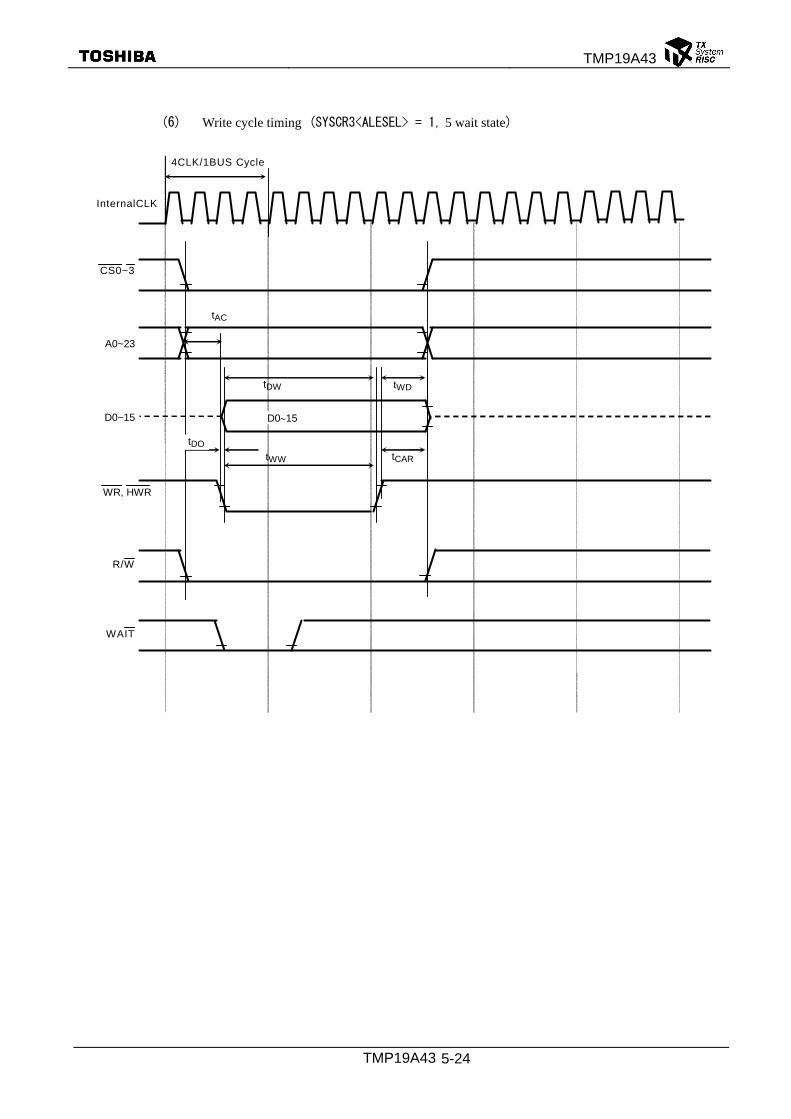
TMP19A43
TMP19A43 5-24
(6) Write cycle timing (SYSCR3<ALESEL> = 1, 5 wait state)
tWW tCAR
tDW
InternalCLK
WR, HWR
CS0~3
R/W
tAC
A0~23
4CLK/1BUS Cycle
tWD
D0∼15 D0~15
tDO
WAIT
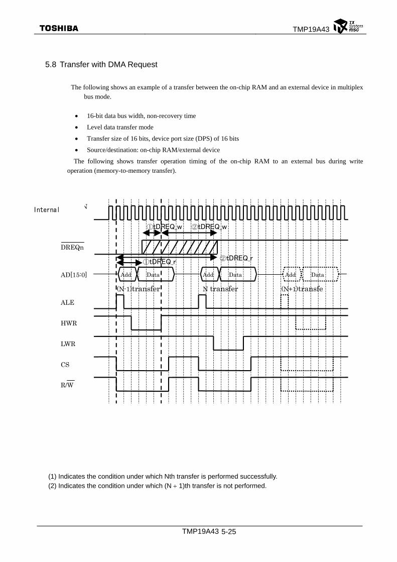
TMP19A43
TMP19A43 5-25
5.8 Transfer with DMA Request
The following shows an example of a transfer between the on-chip RAM and an external device in multiplex
bus mode.
• 16-bit data bus width, non-recovery time
• Level data transfer mode
• Transfer size of 16 bits, device port size (DPS) of 16 bits
• Source/destination: on-chip RAM/external device
The following shows transfer operation timing of the on-chip RAM to an external bus during write
operation (memory-to-memory transfer).
GCLKIN
DREQn
ALE
HWR
LWR
AD[15:0]
N transfer(N-1)transfer (N+1)transfe
CS
①tDREQ_w ②tDREQ_w
R/W
Add Add Add Data Data Data
GACK
2Clk 2Clk
内部的には
GBSTART
②tDREQ_r①tDREQ_r
(1) Indicates the condition under which Nth transfer is performed successfully.
(2) Indicates the condition under which (N + 1)th transfer is not performed.
Internal

TMP19A43
TMP19A43 5-26
DVCC15=CVCCH=1.35Vto1.65V, DVCC3=AVCC3=2.7Vto3.6V,
DAVCC =2.3 Vto2.7V, Ta = -20to85°C
Equation 40 MHz (fsys) Unit
Parameter Symbol
①Min ②Max Min Max
RD asserted to DREQn negated (external device to on-chip RAM transfer)
tDREQ_r (W+1)x (2W+ALE+8)x
-51
50 224 ns
WR / HWR rising to DREQn negated
(on-chip RAM to external device transfer)
tDREQ_w -(W+2)x (5+WAIT)x-51.8 -75 98.2 ns
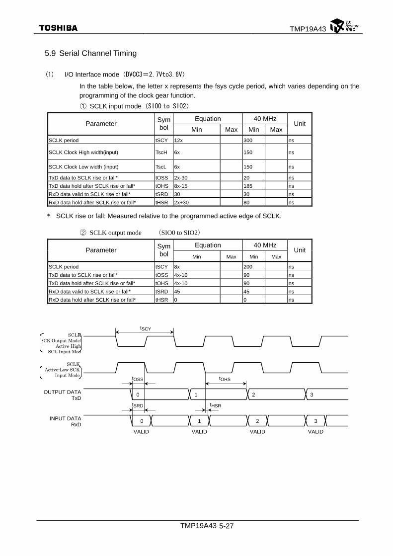
TMP19A43
TMP19A43 5-27
5.9 Serial Channel Timing
(1) I/O Interface mode(DVCC3=2.7Vto3.6V)
In the table below, the letter x represents the fsys cycle period, which varies depending on the
programming of the clock gear function.
① SCLK input mode(SIO0 to SIO2)
Equation 40 MHz Parameter
Symbol Min Max Min Max
Unit
SCLK period tSCY 12x 300 ns
SCLK Clock High width(input) TscH 6x 150 ns
SCLK Clock Low width (input) TscL 6x 150 ns
TxD data to SCLK rise or fall* tOSS 2x-30 20 ns
TxD data hold after SCLK rise or fall* tOHS 8x-15 185 ns
RxD data valid to SCLK rise or fall* tSRD 30 30 ns
RxD data hold after SCLK rise or fall* tHSR 2x+30 80 ns
* SCLK rise or fall: Measured relative to the programmed active edge of SCLK.
② SCLK output mode (SIO0 to SIO2)
Equation 40 MHz Parameter
Symbol Min Max Min Max
Unit
SCLK period tSCY 8x 200 ns
TxD data to SCLK rise or fall* tOSS 4x-10 90 ns
TxD data hold after SCLK rise or fall* tOHS 4x-10 90 ns
RxD data valid to SCLK rise or fall* tSRD 45 45 ns
RxD data hold after SCLK rise or fall* tHSR 0 0 ns
OUTPUT DATATxD
INPUT DATARxD
SCLK SCK Output Mode/
Active-High SCL Input Mod
0
VALID
tOSS
tSCY
tOHS
1 2 3
tSRD tHSR
0 1 2 3
VALID VALID VALID
SCLK Active-Low SCK
Input Mode

TMP19A43
TMP19A43 5-28
5.10 High Speed Serial Channel Timing
(1) I/O Interface mode(DVCC3=2.7V to 3.6V)
In the table below, the letter x represents the fsys cycle period, which varies depending on the
programming of the clock gear function.
① HSCLK input mode(HSIO0 to HSIO2)
Equation 40 MHz Parameter
Symbol Min Max Min Max
Unit
HSCLK period tSCY 12(x/2) 150 ns
HSCLK Clock High width(input) TscH 3x 75 ns
HSCLK Clock Low width (input) TscL 3x 75 ns
TxD data to HSCLK rise or fall* tOSS 2(x/2)-30 -5 ns
TxD data hold after HSCLK rise or fall* tOHS 8(x/2)-15 85 ns
RxD data valid to HSCLK rise or fall* tSRD 30 30 ns
RxD data hold after HSCLK rise or fall* tHSR 2(x/2)+30 55 ns
* HSCLK rise or fall: Measured relative to the programmed active edge of HSCLK.
② HSCLK output mode (HSIO0 to HSIO2)
Equation 40 MHz Parameter
Symbol Min Max Min Max
Unit
HSCLK period tSCY 8(x/2) 100 ns
TxD data to HSCLK rise or fall* tOSS 4(x/2)-10 40 ns
TxD data hold after HSCLK rise or fall* tOHS 4(x/2)-10 40 ns
RxD data valid to HSCLK rise or fall* tSRD 45 45 ns
RxD data hold after HSCLK rise or fall* tHSR 0 0 ns
OUTPUT DATATxD
INPUT DATARxD
SCLK SCK Output Mode/
Active-High SCL Input Mod
0
VALID
tOSS
tSCY
tOHS
1 2 3
tSRD tHSR
0 1 2 3
VALID VALID VALID
SCLK Active-Low SCK
Input Mode

TMP19A43
TMP19A43 5-29
5.11 SBI Timing
(1) I2C mode
In the table below, the letters x represent the fsys periods, respectively.
n denotes the value of n programmed into the SCK (SCL output frequency select) field in the
SBI0CR.
Equation Standard mode Fast mode Parameter Symbol
Min Max Min Max Min Max Unit
SCL clock frequency tSCL 0 0 100 0 400 kHz
Hold time for START condition tHD:STA 4.0 0.6 µs
SCL clock low width (Input) (Note 1) tLOW 4.7 1.3 µs
SCL clock high width (Output) (Note 2) tHIGH 4.0 0.6 µs
Setup time for a repeated START
condition tSU;STA (Note 5) 4.7 0.6 µs
Data hold time (Input) (Note 3, 4) tHD;DAT 0.0 0.0 µs
Data setup time tSU;DAT 250 100 ns
Setup time for STOP condition tSU;STO 4.0 0.6 µs
Bus free time between STOP and
START conditions tBUF (Note 5) 4.7 1.3 µs
Note 1: SCL clock low width (output) is calculated with: (2n-1 +58)/(fsys/2)
Note 2: SCL clock high width (output) is calculated with (2n-1 +12)/(fsys/2)
Note 3: The output data hold time is equal to 12x
Note 4: The Philips I2C-bus specification states that a device must internally provide a hold time of at least
300 ns for the SDA signal to bridge the undefined region of the fall edge of SCL. However, this
SBI does not satisfy this requirement. Also, the output buffer for SCL does not incorporate slope
control of the falling edges; therefore, the equipment manufacturer should design so that the input
data hold time shown in the table is satisfied, including tr/tf of the SCL and SDA lines.
Note 5: Software-dependent
SDA
SCL
tLOW
tHD;STA
tSCL
tHIGHtr
tSU;DAT tHD;DAT tSU;STA tSU;STO tBUF
S: START condition Sr: Repeated START condition P: STOP condition
tf
S Sr P
Notice: On I2C-bus specification, Maximum Speed of Standard Mode is 100KHz ,Fast mode is 400Khz. Internal SCL clock Frequency setting should be shown above Note1 & Note2.

TMP19A43
TMP19A43 5-30
(2) Clock-Synchronous 8-Bit SIO mode
In the tables below, the letters x represent the fsys cycle periods, respectively. The letter n
denotes the value of n programmed into the SCK (SCL output frequency select) field in the
SBI0CR1.
The electrical specifications below are for an SCK signal with a 50% duty cycle.
③ SCK Input mode
Equation 40 MHz Parameter
Symbol Min Max Min Max
Unit
SCK period tSCY 16x 400 ns
SCK Clock High width(input) TscH 8x 200 ns
SCKClock Low width(input) TscH 8x 200 ns
SO data to SCK rise tOSS (tSCY/2) − (6x + 20) 30 ns
SO data hold after SCK rise tOHS (tSCY/2) + 4x 300 ns
SI data valid to SCK rise tSRD 0 0 ns
SI data hold after SCK rise tHSR 4x + 10 110 ns
④ SCK Output mode
Equation 40 MHz Parameter
Symbol Min Max Min Max
Unit
SCK period (programmable) tSCY 2n・T 800 ns
SO data to SCK rise tOSS (tSCY/2) − 20 380 ns
SO data hold after SCK rise tOHS (tSCY/2) − 20 T380 ns
SI data valid to SCK rise tSRD 2x + 30 55 ns
SI data hold after SCK rise tHSR 0 0 ns
OUTPUT DATA TxD
INPUT DATA TxD
SCLK
0
VALID
tOSS
tSCY
tOHS
1 2 3
tSRD tHSR
0 1 2 3
VALID VALID VALID
tSCH
tSCL

TMP19A43
TMP19A43 5-31
5.12 Event Counter
In the table below, the letter x represents the fsys cycle period.
Equation 40 MHz Parameter Symbol
Min Max Min Max Unit
Clock low pulse width tVCKL 2X + 100 150 ns
Clock high pulse width tVCKH 2X + 100 150 ns
5.13 Timer Capture
In the table below, the letter x represents the fsys cycle period.
Equation 40 MHz Parameter Symbol
Min Max Min Max Unit
Low pulse width tCPL 2X + 100 150 ns
High pulse width tCPH 2X + 100 150 ns
5.14 General Interrupts
In the table below, the letter x represents the fsys cycle period.
Equation 40 MHz Parameter Symbol
Min Max Min Max Unit
Low pulse width for INT0-INTA tINTAL X + 100 125 ns
High pulse width for INT0-INTA tINTAH X + 100 125 ns
5.15 STOP /SLEEP/SLOW Wake-up Interrupts
Equation 40 MHz Parameter Symbol
Min Max Min Max Unit
Low pulse width for INT0-INTB tINTBL 100 100 ns
High pulse width for INT0-INTB tINTBH 100 100 ns
5.16 SCOUT Pin
Equation 40 MHz Parameter Symbol
Min Max Min Max Unit
Clock high pulse width tSCH 0.5T − 5 7.5 ns
Clock low pulse width tSCL 0.5T − 5 7.5 ns
Note: In the above table, the letter T represents the cycle period of the SCOUT output clock.
tSCH
tSCLSCOUT

TMP19A43
TMP19A43 5-32
5.17 Bus Request and Bus Acknowledge Signals
tABA
(Note1)
BUSRQ
ALE
A0~A23,
RD , WR
BUSAK
CS0 ~ CS3 ,
W/R , HWR
AD0~AD15
tBAA
(Note2)
(Note2)
Equation 40 MHz Parameter Symbol
Min Max Min Max Unit
Bus float to BUSAK asserted tABA 0 80 0 80 ns
Bus float after BUSAK negated tBAA 0 80 0 80 ns
Note 1: If the current bus cycle has not terminated due to wait-state insertion, the TMP19A43FDXBG does not respond to BUSRQ until the wait state ends.
Note 2: This broken line indicates that output buffers are disabled, not that the signals
are at indeterminate states. The pin holds the last logic value present at that pin
before the bus is relinquished. This is dynamically accomplished through external
load capacitances. The equipment manufacturer may maintain the bus at a
predefined state by means of off-chip restores, but he or she should design,
considering the time (determined by the CR constant) it takes for a signal to
reach a desired state. The on-chip, integrated programmable pullup/pulldown
resistors remain active, depending on internal signal states.

TMP19A43
TMP19A43 5-33
5.18 KWUP Input
Equation 40 MHz Parameter Symbol
Min Max Min Max Unit
Low pulse width for KEY tkyTBL 100 100 ns
High pulse width for KEY tkyTBH 100 100 ns
5.19 Dual Pulse Input
Equation 40 MHz Parameter Symbol
Min Max Min Max Unit
Dual input pulse period Tdcyc 8Y 400 ns
Dual input pulse setup Tabs Y+20 70 ns
Dual input pulse hold Tabh Y+20 70 ns
Y : fsys/2
A
B
5.20 ADTRG input
Equation 40 MHz
Parameter Symbol Min Max Min Max
Unit
Low pulse width for ADTRG tadL fsys/2+
20 32.5 ns
High pulse width for ADTRG Tadh fsys/2+
20 32.5 ns
Tabs
Tabh
Tdcyc

TMP19A43
TMP19A43 5-34
5.21 DSU
Equation 40 MHz Parameter Symbol
Min Max Min Max Unit
PCST valid to DCLK negated Tsetup 11 11 ns
PCST hold after DCLK negated Thold 0.5 0.5 ns
TPC valid to DCLK negated Tsetup 11 11 ns
TPC hold after DCLK negated Thold 0.5 0.5 ns
TPD valid to DCLK negated Tsetup 11 11 ns
TPD hold after DCLK negated Thold 0.5 0.5 ns
OUTPUT DATA PCST,TPC,TPD
DCLK
0
Tsetup
Ttclk
Thold
1 2 3
5.22 EJTAG
Equation 10 MHz(※) Parameter Symbol
Min Max Min Max Unit
TCK valid to TMS/TDI Data in Ttsetup 40 40 ns
TMS/TDI hold after TCK negated Tthold 50 50 ns
TDO hold after TCK asserted Ttout 10 10 ns
※ Operating Frequency of TCK is 10MHz Only
INPUT DATA TMS,TDI
TCK
VALID
Ttclk
tTsetup tThold
0 1 2 3
VALID VALID VALID
OUTPUT DATA TDO
tTOUT


![RISC, CISC, and Assemblers - Cornell University · RISC, CISC, and Assemblers ... • Complexity: CISC, RISC Assemblers ... –e.g. Mem[segment + reg + reg*scale + offset] 14 RISC](https://static.documents.pub/doc/80x56/5c1068af09d3f254228c84fd/risc-cisc-and-assemblers-cornell-risc-cisc-and-assemblers-complexity.jpg)


