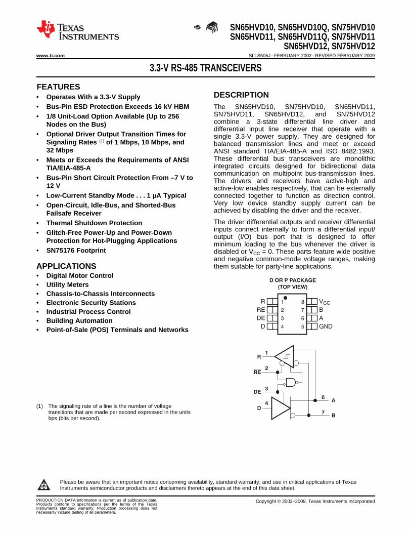
SN65HVD12, SN75HVD12www.ti.com .......................................................................................................................................... SLLS505J–FEBRUARY 2002–REVISED FEBRUARY 2009
3.3-V RS-485 TRANSCEIVERS
• Operates With a 3.3-V Supply• Bus-Pin ESD Protection Exceeds 16 kV HBM The SN65HVD10, SN75HVD10, SN65HVD11,
SN75HVD11, SN65HVD12, and SN75HVD12• 1/8 Unit-Load Option Available (Up to 256combine a 3-state differential line driver andNodes on the Bus)differential input line receiver that operate with a
• Optional Driver Output Transition Times for single 3.3-V power supply. They are designed forSignaling Rates (1) of 1 Mbps, 10 Mbps, and balanced transmission lines and meet or exceed32 Mbps ANSI standard TIA/EIA-485-A and ISO 8482:1993.
These differential bus transceivers are monolithic• Meets or Exceeds the Requirements of ANSIintegrated circuits designed for bidirectional dataTIA/EIA-485-Acommunication on multipoint bus-transmission lines.• Bus-Pin Short Circuit Protection From –7 V to The drivers and receivers have active-high and
12 V active-low enables respectively, that can be externally• Low-Current Standby Mode . . . 1 µA Typical connected together to function as direction control.
Very low device standby supply current can be• Open-Circuit, Idle-Bus, and Shorted-Busachieved by disabling the driver and the receiver.Failsafe ReceiverThe driver differential outputs and receiver differential• Thermal Shutdown Protectioninputs connect internally to form a differential input/• Glitch-Free Power-Up and Power-Down output (I/O) bus port that is designed to offerProtection for Hot-Plugging Applications minimum loading to the bus whenever the driver is
• SN75176 Footprint disabled or VCC = 0. These parts feature wide positiveand negative common-mode voltage ranges, makingthem suitable for party-line applications.
• Digital Motor Control• Utility Meters• Chassis-to-Chassis Interconnects• Electronic Security Stations• Industrial Process Control• Building Automation• Point-of-Sale (POS) Terminals and Networks
(1) The signaling rate of a line is the number of voltagetransitions that are made per second expressed in the unitsbps (bits per second).
1
Please be aware that an important notice concerning availability, standard warranty, and use in critical applications of TexasInstruments semiconductor products and disclaimers thereto appears at the end of this data sheet.
These devices have limited built-in ESD protection. The leads should be shorted together or the device placed in conductive foamduring storage or handling to prevent electrostatic damage to the MOS gates.
ORDERING INFORMATIONPACKAGESIGNALING UNIT LOADS TA SOIC MARKINGRATE SOIC (1) PDIP
–40°C to 125°C10 Mbps 1/8 SN65HVD11QD SN65HVD11QP VP11Q
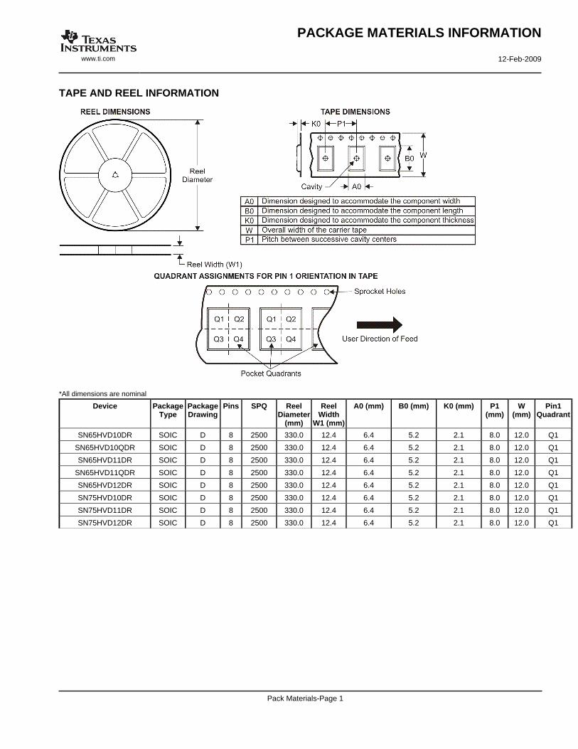
(1) The D package is available taped and reeled. Add an R suffix to the part number (i.e., SN75HVD11DR).
over operating free-air temperature range unless otherwise noted (1) (2)
UNITVCC Supply voltage range –0.3 V to 6 V
Voltage range at A or B –9 V to 14 VInput voltage range at D, DE, R or RE –0.5 V to VCC + 0.5 VVoltage input range, transient pulse, A and B, through 100 Ω, see Figure 11 –50 V to 50 V
IO Receiver output current –11 mA to 11 mAA, B, and GND ±16 kV
Human body model (3)Electrostatic All pins ±4 kVdischargeCharged-device model (4) All pins charge ±1 kV
Continuous total power dissipation See Dissipation Rating TableElectrical Fast Transient/Burst (5) A, B, and GND ±4 kV
TJ Junction temperature 170°C
(1) Stresses beyond those listed under absolute maximum ratings may cause permanent damage to the device. These are stress ratingsonly, and functional operation of the device at these or any other conditions beyond those indicated under recommended operatingconditions is not implied. Exposure to absolute-maximum-rated conditions for extended periods may affect device reliability.
(2) All voltage values, except differential I/O bus voltages, are with respect to network ground terminal.(3) Tested in accordance with JEDEC Standard 22, Test Method A114-A and IEC 60749-26.(4) Tested in accordance with JEDEC Standard 22, Test Method C101.(5) Tested in accordance with IEC 61000-4-4.
PACKAGE TA ≤ 25°C DERATING FACTOR (1) TA = 70°C TA = 85°C TA = 125°CPOWER RATING ABOVE TA = 25°C POWER RATING POWER RATING POWER RATING
(1) This is the inverse of the junction-to-ambient thermal resistance when board-mounted and with no air flow.(2) Tested in accordance with the Low-K thermal metric definitions of EIA/JESD51-3.(3) Tested in accordance with the High-K thermal metric definitions of EIA/JESD51-7.
SN65HVD12, SN75HVD12www.ti.com .......................................................................................................................................... SLLS505J–FEBRUARY 2002–REVISED FEBRUARY 2009
over operating free-air temperature range unless otherwise noted
MIN NOM MAX UNITVCC Supply voltage 3 3.6VI or VIC Voltage at any bus terminal (separately or common mode) –7 (1) 12VIH High-level input voltage D, DE, RE 2 VCC VVIL Low-level input voltage D, DE, RE 0 0.8VID Differential input voltage Figure 7 –12 12
(1) The algebraic convention, in which the least positive (most negative) limit is designated as minimum is used in this data sheet.(2) See thermal characteristics table for information regarding this specification.
over recommended operating conditions unless otherwise noted
PARAMETER TEST CONDITIONS MIN TYP (1) MAX UNITVIK Input clamp voltage II = –18 mA –1.5 V
IO = 0 2 VCC
|VOD| Differential output voltage (2) RL = 54 Ω, See Figure 1 1.5 VVtest = –7 V to 12 V, See Figure 2 1.5
Change in magnitude of differential outputΔ|VOD| See Figure 1 and Figure 2 –0.2 0.2 VvoltageVOC(PP) Peak-to-peak common-mode output voltage 400 mVVOC(SS) Steady-state common-mode output voltage 1.4 2.5 VSee Figure 3
Change in steady-state common-mode output –0.0ΔVOC(SS) 0.05 Vvoltage 5IOZ High-impedance output current See receiver input currents
D –100 0II Input current µA
DE 0 100IOS Short-circuit output current –7 V ≤ VO ≤ 12 V –250 250 mAC(OD) Differential output capacitance VOD = 0.4 sin (4E6πt) + 0.5 V, DE at 0 V 16 pF
RE at VCC, Receiver disabled andD & DE at VCC, 9 15.5 mAdriver enabledNo loadRE at VCC,D at VCC, Receiver disabled andICC Supply current 1 5 µADE at 0 V, driver disabled (standby)No loadRE at 0 V, Receiver enabled andD & DE at VCC, 9 15.5 mAdriver enabledNo load
(1) All typical values are at 25°C and with a 3.3-V supply.(2) For TA > 85°C, VCC is ±5%.
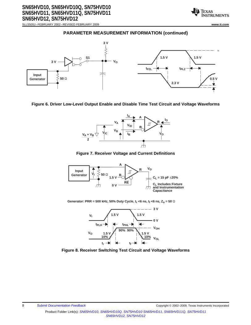
Propagation delay time,tPZH HVD11 55 nshigh-impedance-to-high-level outputHVD12 300RL = 110 Ω, RE at 0 V,
See Figure 5HVD10 25Propagation delay time,tPHZ HVD11 55 nshigh-level-to-high-impedance output
HVD12 300HVD10 26
Propagation delay time,tPZL HVD11 55 nshigh-impedance-to-low-level outputHVD12 300RL = 110 Ω, RE at 0 V,
See Figure 6HVD10 26Propagation delay time,tPLZ HVD11 75 nslow-level-to-high-impedance output
HVD12 400RL = 110 Ω, RE at 3 V,tPZH Propagation delay time, standby-to-high-level output 6 µsSee Figure 5RL = 110 Ω, RE at 3 V,tPZL Propagation delay time, standby-to-low-level output 6 µsSee Figure 6
(1) All typical values are at 25°C and with a 3.3-V supply.(2) tsk(pp) is the magnitude of the difference in propagation delay times between any specified terminals of two devices when both devices
operate with the same supply voltages, at the same temperature, and have identical packages and test circuits.
SN65HVD12, SN75HVD12www.ti.com .......................................................................................................................................... SLLS505J–FEBRUARY 2002–REVISED FEBRUARY 2009
over recommended operating conditions unless otherwise noted
PARAMETER TEST CONDITIONS MIN TYP (1) MAX UNITVIT+ Positive-going input threshold voltage IO = –8 mA -0.01
VNegative-going input thresholdVIT– IO = 8 mA –0.2voltageVhys Hysteresis voltage (VIT+ - VIT-) 35 mVVIK Enable-input clamp voltage II = –18 mA –1.5 VVOH High-level output voltage VID = 200 mV, IOH = –8 mA, See Figure 7 2.4 VVOL Low-level output voltage VID = –200 mV, IOL = 8 mA, See Figure 7 0.4 VIOZ High-impedance-state output current VO = 0 or VCC RE at VCC –1 1 µA
VA or VB = 12 V 0.05 0.11VA or VB = 12 V, VCC = 0 V 0.06 0.13HVD11, HVD12, mAOther input at 0 VVA or VB = –7 V –0.1 –0.05VA or VB = –7 V, VCC = 0 V –0.05 –0.04
II Bus input currentVA or VB = 12 V 0.2 0.5VA or VB = 12 V, VCC = 0 V 0.25 0.5HVD10, mAOther input at 0 VVA or VB = –7 V –0.4 –0.2VA or VB = –7 V, VCC = 0 V –0.4 –0.15
IIH High-level input current, RE VIH = 2 V –30 0 µAIIL Low-level input current, RE VIL = 0.8 V –30 0 µACID Differential input capacitance VID = 0.4 sin (4E6πt) + 0.5 V, DE at 0 V 15 pF
RE at 0 V, Receiver enabled and driverD & DE at 0 V, 4 8 mAdisabledNo loadRE at VCC,D at VCC, Receiver disabled and driverICC Supply current 1 5 µADE at 0 V, disabled (standby)No loadRE at 0 V, Receiver enabled and driverD & DE at VCC, 9 15.5 mAenabledNo load
(1) All typical values are at 25°C and with a 3.3-V supply.
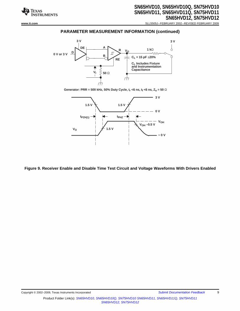
HVD12 15tr Output signal rise time 1 2 5CL = 15 pF, nsSee Figure 8tf Output signal fall time 1 2 5tPZH
(1) Output enable time to high level 15tPZL
(1) Output enable time to low level 15CL = 15 pF, DE at 3 V, nsSee Figure 9tPHZ Output disable time from high level 20tPLZ Output disable time from low level 15tPZH
(2) Propagation delay time, standby-to-high-level output 6CL = 15 pF, DE at 0, µsSee Figure 10tPZL(2) Propagation delay time, standby-to-low-level output 6
(1) All typical values are at 25°C and with a 3.3-V supply(2) tsk(pp) is the magnitude of the difference in propagation delay times between any specified terminals of two devices when both devices
operate with the same supply voltages, at the same temperature, and have identical packages and test circuits.
over operating free-air temperature range unless otherwise noted (1)
PARAMETER TEST CONDITIONS MIN TYP MAX UNITHigh−K board (3), No airflow D pkg 121Junction−to−ambient thermalθJA resistance (2) No airflow (4) P pkg 93High−K board D pkg 67Junction−to−board thermalθJB °C/Wresistance See (4) P pkg 57
D pkg 41Junction−to−case thermalθJC resistance P pkg 55HVD10 198 250(32 Mbps)RL= 60 Ω, CL = 50 pF,
DE at VCC, RE at 0 V, HVD11 141 176PD Device power dissipation mWInput to D a 50% duty cycle square (10 Mbps)wave at indicated signaling rate HVD12 133 161
(500 kbps)High−K board, No airflow D pkg –40 116
TA Ambient air temperatureNo airflow (4) P pkg –40 123 °C
TJSD Thermal shutdown junction temperature 165
(1) See Application Information section for an explanation of these parameters.(2) The intent of θJA specification is solely for a thermal performance comparison of one package to another in a standardized environment.
This methodology is not meant to and will not predict the performance of a package in an application-specific environment.(3) JSD51−7, High Effective Thermal Conductivity Test Board for Leaded Surface Mount Packages.(4) JESD51−10, Test Boards for Through-Hole Perimeter Leaded Package Thermal Measurements.
NOTE: The line should be terminated at both ends with its characteristic impedance (RT = ZO). Stub lengths off the main lineshould be kept as short as possible.
Figure 24. HVD12 Input and Output Through 2000 Feet of Cable
length of Commscope 5524 category 5e+ twisted pairAn example application for the HVD12 is illustrated in cable. The bus is terminated at each end by a 100-ΩFigure 23. Two HVD12 transceivers are used to resistor, matching the cable characteristic impedance.communicate data through a 2000 foot (600 m) Figure 24 illustrates operation at a signaling rate of250 kbps.
SN65HVD12, SN75HVD12www.ti.com .......................................................................................................................................... SLLS505J–FEBRUARY 2002–REVISED FEBRUARY 2009
θJC (Junction-to-Case Thermal Resistance) isPACKAGES defined as difference in junction temperature to case
divided by the operating power. It is measured byθJA (Junction-to-Ambient Thermal Resistance) is putting the mounted package up against a copperdefined as the difference in junction temperature to block cold plate to force heat to flow from die, throughambient temperature divided by the operating power. the mold compound into the copper block.θJA is not a constant and is a strong function of: θJC is a useful thermal characteristic when a heatsink• the PCB design (50% variation) is applied to package. It is not a useful characteristic• altitude (20% variation) to predict junction temperature because it provides
pessimistic numbers if the case temperature is• device power (5% variation)measured in a nonstandard system and junction
θJA can be used to compare the thermal performance temperatures are backed out. It can be used with θJBof packages if the specific test conditions are defined in 1-dimensional thermal simulation of a packageand used. Standardized testing includes specification system.of PCB construction, test chamber volume, sensor
θJB (Junction-to-Board Thermal Resistance) islocations, and the thermal characteristics of holdingdefined as the difference in the junction temperaturefixtures. θJA is often misused when it is used toand the PCB temperature at the center of thecalculate junction temperatures for other installations.package (closest to the die) when the PCB is
TI uses two test PCBs as defined by JEDEC clamped in a cold-plate structure. θJB is only definedspecifications. The low-k board gives average in-use for the high-k test card.condition thermal performance, and it consists of a
θJB provides an overall thermal resistance betweensingle copper trace layer 25 mm long and 2-oz thick.the die and the PCB. It includes a bit of the PCBThe high-k board gives best case in-use condition,thermal resistance (especially for BGA’s with thermaland it consists of two 1-oz buried power planes with aballs) and can be used for simple 1-dimensionalsingle copper trace layer 25 mm long and 2-oz thick.network analysis of package system, see Figure 25.A 4% to 50% difference in θJA can be measured
Orderable Device Status (1) Package Type PackageDrawing
Pins Package Qty Eco Plan (2) Lead/Ball Finish
MSL Peak Temp (3) Samples
(Requires Login)
SN75HVD12D ACTIVE SOIC D 8 75 Green (RoHS& no Sb/Br)
CU NIPDAU Level-1-260C-UNLIM Purchase Samples
SN75HVD12DG4 ACTIVE SOIC D 8 75 Green (RoHS& no Sb/Br)
CU NIPDAU Level-1-260C-UNLIM Purchase Samples
SN75HVD12DR ACTIVE SOIC D 8 2500 Green (RoHS& no Sb/Br)
CU NIPDAU Level-1-260C-UNLIM Purchase Samples
SN75HVD12DRG4 ACTIVE SOIC D 8 2500 Green (RoHS& no Sb/Br)
CU NIPDAU Level-1-260C-UNLIM Purchase Samples
SN75HVD12P ACTIVE PDIP P 8 50 Pb-Free (RoHS) CU NIPDAU N / A for Pkg Type Request Free Samples
SN75HVD12PE4 ACTIVE PDIP P 8 50 Pb-Free (RoHS) CU NIPDAU N / A for Pkg Type Request Free Samples (1) The marketing status values are defined as follows:ACTIVE: Product device recommended for new designs.LIFEBUY: TI has announced that the device will be discontinued, and a lifetime-buy period is in effect.NRND: Not recommended for new designs. Device is in production to support existing customers, but TI does not recommend using this part in a new design.PREVIEW: Device has been announced but is not in production. Samples may or may not be available.OBSOLETE: TI has discontinued the production of the device.
(2) Eco Plan - The planned eco-friendly classification: Pb-Free (RoHS), Pb-Free (RoHS Exempt), or Green (RoHS & no Sb/Br) - please check http://www.ti.com/productcontent for the latest availabilityinformation and additional product content details.TBD: The Pb-Free/Green conversion plan has not been defined.Pb-Free (RoHS): TI's terms "Lead-Free" or "Pb-Free" mean semiconductor products that are compatible with the current RoHS requirements for all 6 substances, including the requirement thatlead not exceed 0.1% by weight in homogeneous materials. Where designed to be soldered at high temperatures, TI Pb-Free products are suitable for use in specified lead-free processes.Pb-Free (RoHS Exempt): This component has a RoHS exemption for either 1) lead-based flip-chip solder bumps used between the die and package, or 2) lead-based die adhesive used betweenthe die and leadframe. The component is otherwise considered Pb-Free (RoHS compatible) as defined above.Green (RoHS & no Sb/Br): TI defines "Green" to mean Pb-Free (RoHS compatible), and free of Bromine (Br) and Antimony (Sb) based flame retardants (Br or Sb do not exceed 0.1% by weightin homogeneous material)
(3) MSL, Peak Temp. -- The Moisture Sensitivity Level rating according to the JEDEC industry standard classifications, and peak solder temperature.
Important Information and Disclaimer:The information provided on this page represents TI's knowledge and belief as of the date that it is provided. TI bases its knowledge and belief on informationprovided by third parties, and makes no representation or warranty as to the accuracy of such information. Efforts are underway to better integrate information from third parties. TI has taken andcontinues to take reasonable steps to provide representative and accurate information but may not have conducted destructive testing or chemical analysis on incoming materials and chemicals.TI and TI suppliers consider certain information to be proprietary, and thus CAS numbers and other limited information may not be available for release.
In no event shall TI's liability arising out of such information exceed the total purchase price of the TI part(s) at issue in this document sold by TI to Customer on an annual basis.
OTHER QUALIFIED VERSIONS OF SN65HVD10, SN65HVD12 :
Texas Instruments Incorporated and its subsidiaries (TI) reserve the right to make corrections, modifications, enhancements, improvements,and other changes to its products and services at any time and to discontinue any product or service without notice. Customers shouldobtain the latest relevant information before placing orders and should verify that such information is current and complete. All products aresold subject to TI’s terms and conditions of sale supplied at the time of order acknowledgment.
TI warrants performance of its hardware products to the specifications applicable at the time of sale in accordance with TI’s standardwarranty. Testing and other quality control techniques are used to the extent TI deems necessary to support this warranty. Except wheremandated by government requirements, testing of all parameters of each product is not necessarily performed.
TI assumes no liability for applications assistance or customer product design. Customers are responsible for their products andapplications using TI components. To minimize the risks associated with customer products and applications, customers should provideadequate design and operating safeguards.
TI does not warrant or represent that any license, either express or implied, is granted under any TI patent right, copyright, mask work right,or other TI intellectual property right relating to any combination, machine, or process in which TI products or services are used. Informationpublished by TI regarding third-party products or services does not constitute a license from TI to use such products or services or awarranty or endorsement thereof. Use of such information may require a license from a third party under the patents or other intellectualproperty of the third party, or a license from TI under the patents or other intellectual property of TI.
Reproduction of TI information in TI data books or data sheets is permissible only if reproduction is without alteration and is accompaniedby all associated warranties, conditions, limitations, and notices. Reproduction of this information with alteration is an unfair and deceptivebusiness practice. TI is not responsible or liable for such altered documentation. Information of third parties may be subject to additionalrestrictions.
Resale of TI products or services with statements different from or beyond the parameters stated by TI for that product or service voids allexpress and any implied warranties for the associated TI product or service and is an unfair and deceptive business practice. TI is notresponsible or liable for any such statements.
TI products are not authorized for use in safety-critical applications (such as life support) where a failure of the TI product would reasonablybe expected to cause severe personal injury or death, unless officers of the parties have executed an agreement specifically governingsuch use. Buyers represent that they have all necessary expertise in the safety and regulatory ramifications of their applications, andacknowledge and agree that they are solely responsible for all legal, regulatory and safety-related requirements concerning their productsand any use of TI products in such safety-critical applications, notwithstanding any applications-related information or support that may beprovided by TI. Further, Buyers must fully indemnify TI and its representatives against any damages arising out of the use of TI products insuch safety-critical applications.
TI products are neither designed nor intended for use in military/aerospace applications or environments unless the TI products arespecifically designated by TI as military-grade or "enhanced plastic." Only products designated by TI as military-grade meet militaryspecifications. Buyers acknowledge and agree that any such use of TI products which TI has not designated as military-grade is solely atthe Buyer's risk, and that they are solely responsible for compliance with all legal and regulatory requirements in connection with such use.
TI products are neither designed nor intended for use in automotive applications or environments unless the specific TI products aredesignated by TI as compliant with ISO/TS 16949 requirements. Buyers acknowledge and agree that, if they use any non-designatedproducts in automotive applications, TI will not be responsible for any failure to meet such requirements.
Following are URLs where you can obtain information on other Texas Instruments products and application solutions:


![Point-to-Multipoint and Multipoint-to-Multipoint · PDF filedefined by IEEE 802.1Qay [2] is representative carrier Ethernet . Abstract — We have implemented point-to-multipoint (PtMP)](https://static.documents.pub/doc/80x56/5a75c0147f8b9a4b538cb6cd/point-to-multipoint-and-multipoint-to-multipoint-defined-by-ieee-8021qay.jpg)

