372 IEEE TRANSACTIONS ON VERY LARGE SCALE INTEGRATION (VLSI) SYSTEMS, VOL. 22, NO. 2, FEBRUARY 2014
Split-SAR ADCs: Improved Linearity WithPower and Speed Optimization
Yan Zhu, Chi-Hang Chan, U-Fat Chio, Sai-Weng Sin, Seng-Pan U, Rui Paulo Martins, and Franco Maloberti
Abstract— This paper presents the linearity analysis ofa successive approximation registers (SAR) analog-to-digitalconverters (ADC) with split DAC structure based on twoswitching methods: conventional charge-redistribution andVcm-based switching. The static linearity performance, namelythe integral nonlinearity and differential nonlinearity, as well asthe parasitic effects of the split DAC, are analyzed hereunder. Inaddition, a code-randomized calibration technique is proposedto correct the conversion nonlinearity in the conventional SARADC, which is verified by behavioral simulations, as well asmeasured results. Performances of both switching methods aredemonstrated in 90 nm CMOS. Measurement results of power,speed, and linearity clearly show the benefits of using Vcm-basedswitching.
SUCCESSIVE approximation registers (SAR)analog-to-digital converters (ADCs) [1]–[4], as an
alternative to the pipelined ADCs [5]–[9] has become popularfor battery-powered mobile applications, such as DVB-T,DVB-H and TDMB [10], [11] which require medium speed(10 MS/s–100 MS/s) and medium-resolution (8–10 b). SARADCs [2]–[4] achieve very low power consumption due totheir simple architecture and operation. However, the SARconversion relies basically on the performance of a capacitiveDAC that subtracts the reference voltage from the inputsignal. The kT/C noise, capacitor mismatches, and parasiticof the split DAC [12] affect the conversion accuracy. As formedium resolution, the kT/C noise requirement is fulfilledwith small capacitance, while other nonidealities like parasiticand nonlinearity, whose effect depends on the structure andthe switching approach of the DAC, becomes significant.
Manuscript received May 29, 2012; revised December 13, 2012; acceptedJanuary 8, 2013. Date of publication February 14, 2013; date of currentversion January 17, 2014. This work was supported in part by the ResearchCommittee of the University of Macau and the Macao Science and TechnologyDevelopment Fund.
Y. Zhu, C.-H. Chan, U. F. Chio, S. W. Sin, and S. P. U are withthe State-Key-Laboratory Analog and Mixed-Signal VLSI, Faculty ofScience and Technology, University of Macau, Macao 853, China (e-mail:[email protected]).
R. P. Martins is with the State-Key-Laboratory Analog and Mixed-SignalVLSI, Faculty of Science and Technology, University of Macau, Macao 853,China, and also with the Instituto Superior Técnico/TU, Lisbon 1049-001,Portugal (e-mail: [email protected]).
F. Maloberti is with the Department of Electronics, University of Pavia,Pavia 27100, Italy (e-mail: [email protected]).
Color versions of one or more of the figures in this paper are availableonline at http://ieeexplore.ieee.org.
Digital Object Identifier 10.1109/TVLSI.2013.2242501
The binary-weighted capacitive DAC is widely used inSAR ADCs. However, the capacitance of the DAC arrayincreases exponentially with the resolution, which imposeslarger consumption of switching energy, area, and settlingtime. A valuable substitute is the split capacitive DAC,which has been recently reconsidered for medium resolution[13]–[18]. Its key limitation lies in the parasitic capacitorsthat destroy the desired binary ratio of the capacitive DACarray, thus degrading the conversion linearity. However, byusing the metal-insulator-metal (MIM) capacitor or/and DACmismatch calibrations [19]–[22], the split structure can becomesuitable for a medium-resolution target. On the other hand,the conversion linearity is also directly correlated with theswitching sequences of the DAC array [12], [23], where theconventional charge-redistribution switching results in worseconversion linearity and more energy losses. A Vcm-basedswitching technique has been recently proposed [24], whichachieves a significant switching energy saving when comparedwith set-and-down [3] and charge-recycling [25] switchingapproaches.
This paper analyzes the conversion nonlinearities, inducedby supply noise, switching methods, and parasitic effectsin SAR ADCs. The static nonlinearities based on theconventional and Vcm-based [24] switching methods aretheoretically analyzed, and the mathematical models aredeveloped to verify the effectiveness of the Vcm-basedapproach. Experimental results on a 90 nm CMOS 10 b65 MS/s SAR ADC with conventional switching and a 10 b100 MS/s SAR ADC with Vcm-based switching demonstratethe performance benefits in terms of speed, power, andlinearity by using Vcm-based switching.
In addition, the internal node parasitic in the split DACis also analyzed, as it degrades the conversion linearity. Theabove limitation can be fixed by a code-randomized digitalcalibration technique proposed here to improve the differentialnonlinearity (DNL) and integral nonlinearity (INL).
Section II presents the overall SAR ADC architecture;Section III introduces the conventional and Vcm-basedswitching approaches. Section IV provides an analyticalanalysis of the static nonlinearity due to the capacitormismatch and the parasitic effects in the two methods, andit also includes the behavioral simulations for confirmationof results. Finally, a DNL and INL calibration technique forparasitic nonlinearity in split DAC is proposed in section V.The measurement results of two integrated SAR ADCs and theconclusions are presented in Sections VI and VII, respectively.
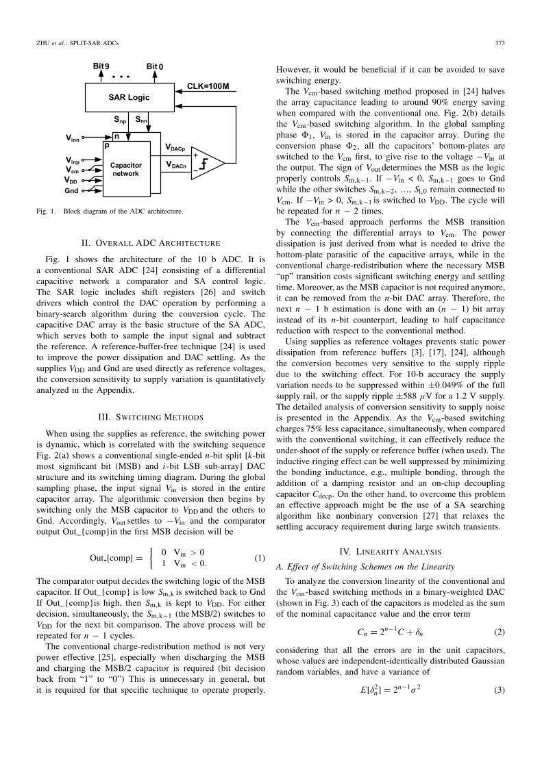
Fig. 1 shows the architecture of the 10 b ADC. It isa conventional SAR ADC [24] consisting of a differentialcapacitive network a comparator and SA control logic.The SAR logic includes shift registers [26] and switchdrivers which control the DAC operation by performing abinary-search algorithm during the conversion cycle. Thecapacitive DAC array is the basic structure of the SA ADC,which serves both to sample the input signal and subtractthe reference. A reference-buffer-free technique [24] is usedto improve the power dissipation and DAC settling. As thesupplies VDD and Gnd are used directly as reference voltages,the conversion sensitivity to supply variation is quantitativelyanalyzed in the Appendix.
III. SWITCHING METHODS
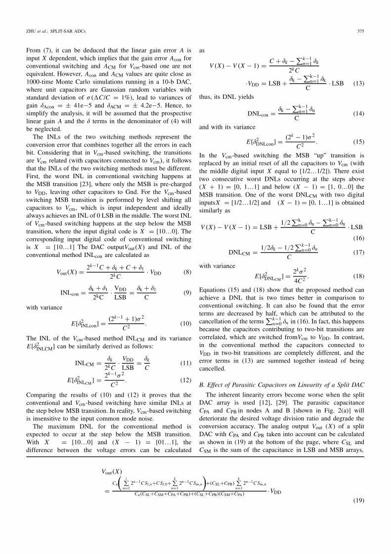
When using the supplies as reference, the switching poweris dynamic, which is correlated with the switching sequenceFig. 2(a) shows a conventional single-ended n-bit split [k-bitmost significant bit (MSB) and i -bit LSB sub-array] DACstructure and its switching timing diagram. During the globalsampling phase, the input signal Vin is stored in the entirecapacitor array. The algorithmic conversion then begins byswitching only the MSB capacitor to VDD and the others toGnd. Accordingly, Vout settles to −Vin and the comparatoroutput Out_{comp}in the first MSB decision will be
Out {comp} =!
0 Vin > 01 Vin < 0.
(1)
The comparator output decides the switching logic of the MSBcapacitor. If Out_{comp} is low Sm,k is switched back to GndIf Out_{comp}is high, then Sm,k is kept to VDD. For eitherdecision, simultaneously, the Sm,k−1 (the MSB/2) switches toVDD for the next bit comparison. The above process will berepeated for n − 1 cycles.
The conventional charge-redistribution method is not verypower effective [25], especially when discharging the MSBand charging the MSB/2 capacitor is required (bit decisionback from “1” to “0”) This is unnecessary in general, butit is required for that specific technique to operate properly.
However, it would be beneficial if it can be avoided to saveswitching energy.
The Vcm-based switching method proposed in [24] halvesthe array capacitance leading to around 90% energy savingwhen compared with the conventional one. Fig. 2(b) detailsthe Vcm-based switching algorithm. In the global samplingphase !1, Vin is stored in the capacitor array. During theconversion phase !2, all the capacitors’ bottom-plates areswitched to the Vcm first, to give rise to the voltage −Vin atthe output. The sign of Vout determines the MSB as the logicproperly controls Sm,k−1. If −Vin < 0, Sm,k−1 goes to Gndwhile the other switches Sm,k−2, …, Sl,0 remain connected toVcm. If −Vin > 0, Sm,k−1 is switched to VDD. The cycle willbe repeated for n − 2 times.
The Vcm-based approach performs the MSB transitionby connecting the differential arrays to Vcm. The powerdissipation is just derived from what is needed to drive thebottom-plate parasitic of the capacitive arrays, while in theconventional charge-redistribution where the necessary MSB“up” transition costs significant switching energy and settlingtime. Moreover, as the MSB capacitor is not required anymore,it can be removed from the n-bit DAC array. Therefore, thenext n − 1 b estimation is done with an (n − 1) bit arrayinstead of its n-bit counterpart, leading to half capacitancereduction with respect to the conventional method.
Using supplies as reference voltages prevents static powerdissipation from reference buffers [3], [17], [24], althoughthe conversion becomes very sensitive to the supply rippledue to the switching effect. For 10-b accuracy the supplyvariation needs to be suppressed within ±0.049% of the fullsupply rail, or the supply ripple ±588 µV for a 1.2 V supply.The detailed analysis of conversion sensitivity to supply noiseis presented in the Appendix. As the Vcm-based switchingcharges 75% less capacitance, simultaneously, when comparedwith the conventional switching, it can effectively reduce theunder-shoot of the supply or reference buffer (when used). Theinductive ringing effect can be well suppressed by minimizingthe bonding inductance, e.g., multiple bonding, through theaddition of a damping resistor and an on-chip decouplingcapacitor Cdecp. On the other hand, to overcome this probleman effective approach might be the use of a SA searchingalgorithm like nonbinary conversion [27] that relaxes thesettling accuracy requirement during large switch transients.
IV. LINEARITY ANALYSIS
A. Effect of Switching Schemes on the Linearity
To analyze the conversion linearity of the conventional andthe Vcm-based switching methods in a binary-weighted DAC(shown in Fig. 3) each of the capacitors is modeled as the sumof the nominal capacitance value and the error term
Cn = 2n−1C + δn (2)
considering that all the errors are in the unit capacitors,whose values are independent-identically distributed Gaussianrandom variables, and have a variance of
E[δ2n] = 2n−1σ 2 (3)
374 IEEE TRANSACTIONS ON VERY LARGE SCALE INTEGRATION (VLSI) SYSTEMS, VOL. 22, NO. 2, FEBRUARY 2014
Sample Φ1
MSB Array LSB ArrayCa
2i-1CVout
C CSl,0Sl,1Sl,i
C
Convert Φ2
Φ1
VcmΦ1 Vin
GndVDD{Φ2
V cm -based sw itch ing rem oves the M S B capacito r in D A C
Sample Φ1
MSB Array LSB ArrayCa
CVout
C CSl,0Sl,1Sl,i
CC
Sm,1
Convert Φ2
Φ1
VcmVin
GndVDD{Φ2
2k-1C
Sm,k
Φ1{
2k-2
Sm,k-1
Sm,k
2k-1C
Sm,k-1
2k-2C
Sm,1
Sm,k-1
Sm,k-2
2i-1
Sm,k
Sm,k-1
VDD VDD/Gnd
VDD VDD/Gnd
Vcm
Vcm
VDD/Gnd
Comp.
Comp.
VDD/Gnd
Gnd
ACPA BCPB
ACPA BCPB
(a)
(b)
Fig. 2. Single-ended n-bit and (n − 1)-bit split capacitive DAC arrays with their switching timing diagrams (n = k + i). (a) Conventional switching.(b) Vcm-based switching.
VoutC
S0
CC
S1
VcmVin
GndVDD
2k-1 C
Sk
2k-2
Sk-1
Fig. 3. k-bit binary-weighted DAC.
and where σ is the standard deviation of the unit capacitor.The Vcm-based method achieves half capacitance reductionwhen compared with the conventional one, while the switchinglinearity comparison between the two switching methodsshould be addressed in the same capacitive DAC, with thesame value of capacitor mismatch as well as predictable gainerrors caused by unbalanced array capacitance. Accordingly,to perform the Vcm-based switching method in the k-bit DACarray of Fig. 3, both S0 and S1 are kept connected to Vcmduring bits cycling.
To calculate a given digital input X with its correspondingDAC output Vout (X), the array is considered initially
discharged (Vin = 0). The analog output of the k-bit capacitiveDAC with conventional switching can be calculated as
Vout(X) ="k
n=1 (2n−1C + δn)Sn + (C + δ0)S0
2kC + "kn=0 δn
· VDD (4)
where the DAC digital input X = [Sn…S0], with Sn equalto 1, 1/2 or 0 represents the DAC connecting VDD, 1/2 VDD(i.e., Vcm) or Gnd for bit n. For a single channel SAR ADC,the comparator offset and linear gain error in the DAC areacceptable, thus closed form calculations of INL and DNL arespecified with respect to a bestfit line. In the SAR conversion,the comparator offset appears as an offset error and does notcause nonlinearity, therefore, excluding the offset term, theINL and DNL are [28]
INL = Vout(X)/A − Vidl(X)
LSB(5)
DNL = [Vout(X) − Vout(X − 1)]/A − LSBLSB
(6)
A ="2n−1
X=0 Vout(X) · Vidl(X)"2n−1
X=0 V 2idl(X)
(7)
where A indicates the linear gain error of the DAC, Vidl(X) isthe nominal value for the digital input X and LSB = 1/2kVDD.
ZHU et al.: SPLIT-SAR ADCs 375
From (7), it can be deduced that the linear gain error A isinput X dependent, which implies that the gain error Acon forconventional switching and ACM for Vcm-based one are notequivalent. However, Acon and ACM values are quite close as1000-time Monte Carlo simulations running in a 10-b DAC,where unit capacitors are Gaussian random variables withstandard deviation of σ ($C/C = 1%), lead to variances ofgain δAcon = ± 41e−5 and δACM = ± 4.2e−5. Hence, tosimplify the analysis, it will be assumed that the prospectivelinear gain A and the δ terms in the denominator of (4) willbe neglected.
The INLs of the two switching methods represent theconversion error that combines together all the errors in eachbit. Considering that in Vcm-based switching, the transitionsare Vcm related (with capacitors connected to Vcm), it followsthat the INLs of the two switching methods must be different.First, the worst INL in conventional switching happens atthe MSB transition [23], where only the MSB is pre-chargedto VDD, leaving other capacitors to Gnd. For the Vcm-basedswitching MSB transition is performed by level shifting allcapacitors to Vcm, which is input independent and ideallyalways achieves an INL of 0 LSB in the middle. The worst INLof Vcm-based switching happens at the step below the MSBtransition, where the input digital code is X = [10…0]. Thecorresponding input digital code of conventional switchingis X = [10…1] The DAC outputVout(X) and INL of theconventional method INLcon are calculated as
Vout(X) = 2k−1C + δk + C + δ1
2kC· VDD (8)
INLcon = δk + δ1
2kC· VDD
LSB= δk + δ1
C(9)
with variance
E[δ2INLcon] = (2k−1 + 1)σ 2
C2 . (10)
The INL of the Vcm-based method INLCM and its varianceE[δ2
INLCM] can be similarly derived as follows:
INLCM = δk
2kC· VDD
LSB= δk
C(11)
E[δ2INLCM
] = 2k−1σ 2
C2 . (12)
Comparing the results of (10) and (12) it proves that theconventional and Vcm-based switching have similar INLs atthe step below MSB transition. In reality, Vcm-based switchingis insensitive to the input common mode noise.
The maximum DNL for the conventional method isexpected to occur at the step below the MSB transition.With X = [10…0] and (X − 1) = [01…1], thedifference between the voltage errors can be calculated
Vout(X)
=Ca
#i"
n=12n−1C Sl,n+C Sl,0+
k"
n=12n−1C Sm,n
$
+(CSL+CPB)k"
n=12n−1C Sm,n
Ca(CSL+CSM+CPA+CPB)+(CSL+CPB)(CSM+CPA) ·VDD
(19)
as
V (X) − V (X − 1) = C + δk − "k−1n=1 δk
2kC
·VDD = LSB + δk − "k−1n=1 δk
C· LSB (13)
thus, its DNL yields
DNLcon = δk − "k−1n=1 δn
C(14)
and with its variance
E[δ2DNLcon] = (2k − 1)σ 2
C2 . (15)
In the Vcm-based switching the MSB “up” transition isreplaced by an initial reset of all the capacitors to Vcm (withthe middle digital input X equal to [1/2…1/2]). There existtwo consecutive worst DNLs occurring at the steps above(X + 1) = [0, 1…1] and below (X − 1) = [1, 0…0] theMSB transition. One of the worst DNLCM with two digitalinputsX = [1/2…1/2] and (X − 1) = [0, 1…1] is obtainedsimilarly as
V (X) − V (X − 1) = LSB + 1/2"k
n=0 δn − "k−1n=0 δn
C· LSB
(16)
DNLCM = 1/2δk − 1/2"k−1
n=0 δn
C(17)
with variance
E[δ2DNLCM
] = 2kσ 2
4C2 . (18)
Equations (15) and (18) show that the proposed method canachieve a DNL that is two times better in comparison toconventional switching. It can also be found that the errorterms are decreased by half, which can be attributed to thecancellation of the terms
"k−1n=0 δn in (16). In fact, this happens
because the capacitors contributing to two-bit transitions arecorrelated, which are switched fromVcm to VDD. In contrast,in the conventional method the capacitors connected toVDD in two-bit transitions are completely different, and theerror terms in (13) are summed together instead of beingcancelled.
B. Effect of Parasitic Capacitors on Linearity of a Split DAC
The inherent linearity errors become worse when the splitDAC array is used [12], [29]. The parasitic capacitanceCPA and CPB in nodes A and B [shown in Fig. 2(a)] willdeteriorate the desired voltage division ratio and degrade theconversion accuracy. The analog output Vout (X) of a splitDAC with CPA and CPB taken into account can be calculatedas shown in (19) at the bottom of the page, where CSL andCSM is the sum of the capacitance in LSB and MSB arrays,
376 IEEE TRANSACTIONS ON VERY LARGE SCALE INTEGRATION (VLSI) SYSTEMS, VOL. 22, NO. 2, FEBRUARY 2014
respectively. The parasitic capacitor CPB in the numeratorchanges the value of second term. The CPA and CPB in thedenominator cause a gain error which is irrelevant in theanalysis. Subtracting the nominal value, the error term of theMSB/2 transition (X = [010…0]) in the conventional methodis given by
Verr(X)con = CPB2k−2CCa(CSL + CSM) + CSLCSM
· VDD. (20)
Correspondingly, for the Vcm-based method, the error term atthe MSB/2 transition (X = [0, 1/2…1/2]) is obtained as
Verr(X)CM = CPB(2k−1−1)CCa(CSL+CSM)+CSLCSM
· VDD2
= CPB(2k−2−1/2)CCa(CSL+CSM)+CSLCSM
· VDD. (21)
From (20) and (21), it can be concluded that the Vcm-basedand the conventional switching have a similar INL.
The increased DNL due to the CPB is expected tohappen at the step below the last bit transition of theMSB array. Considering the 10-b split DAC of Fig. 2(a)with 5 b of MSB array and 5 b of LSB array, twoconsecutive digital inputs for the conventional method are:X = [0000100000]→ → (X − 1) = [0000011111], andfor the Vcm-based are: X = [0000, 1/2, 1/2, 1/2, 1/2, 1/2,1/2] → → (X − 1) = [0000011111]. On the other hand,the error term CPB in (19) is only correlated with the bitsin the MBS array. Accordingly, the difference between thetwo voltage errors is only caused by the bit Sm,1 in X . Inconclusion, the voltage errors for conventional and Vcm-basedswitching can be simply derived as
Verr,con = CPBCCa(CSL + CSM) + CSLCSM
· VDD (22)
Verr,CM = CPBCCa(CSL + CSM) + CSLCSM
· VDD
2. (23)
As a consequence of (22) and (23), Vcm-based switchingreduces the DNL by half when compared with the conventionalswitching. This benefit can be explained by the switchingnature of the Vcm-based method, which divides half of thevoltage contribution from the last bit of the MSB array, whichis CPB related, to all the capacitors in the LSB array that areirrelevant to CPB. Table I summarizes the switching linearityof the two methods.
C. Behavioral Simulations
To verify the previous analysis, behavioral simulations wereperformed which modeled the conversion linearity of theconventional and Vcm-based switching methods in a 10 b splitDAC array with 5 b MSB and 5 b LSB arrays. The valuesof the unit capacitor are Gaussian random variables with astandard deviation of σ ($C/C = 1%), and the parasiticcapacitance is not considered. Fig. 4 illustrates the result of1000-sample Monte Carlo runs, where the standard deviationsof DNLs and INLs with respect to a best fit line are plottedversus the DAC input code at 10-b level. As expected, twomethods have similarly large INLs, while Vcm-based switchinghas lower INLs at the transitions where the input code is morerelevant to Vcm. This happens in the cases like the transitions
TABLE I
SWITCHING LINEARITY COMPARISON BETWEEN CONVENTIONAL &
VCM-BASED METHODS
0 100 200 300 400 500 600 700 800 900 1000
0.020.040.060.080.1
0.120.140.160.18
Input Digital Code X
Stan
dard
Dev
iatio
nof
INL(
LSB)
Stan
dard
Dev
iatio
nof
DN
L(LS
B)
Input Digital Code X
Vcm-basedConv.
0
MSB/2Transition
MSB Transition
0 100 200 300 400 500 600 700 800 900 10000
0.05
0.1
0.15
0.2
0.25
0.3
0.35Vcm-based
Conv.
(a)
(b)
Fig. 4. Behavioral simulation comparing the DNL and INL of conventionaland Vcm-based 10-b SAR ADCs.
of MSB and MSB/2. The DNL plot shown in Fig. 4(b)confirms the presented analysis of Vcm-based switching thatdenotes two consecutive high DNLs at the middle. Their valueis two times lower than its conventional counterpart.
The simulation estimates the effect of the parasitic capacitorin the split structure supposing 10% top-plate parasitic withmatched capacitor. The DNLs and INLs results of conventionaland Vcm-based switching methods obtained by 100 000 pointswith sine wave input are shown in Fig. 5. The maximum DNLsand INLs of conventional and Vcm-based switching are 2.9
ZHU et al.: SPLIT-SAR ADCs 377
(a)
(b)
Fig. 5. Behavioral simulation results of DNLs and INLs for 10-b SAR ADCswith CPB. (a) Conventional switching. (b) Vcm-based switching.
LSB/1.5 LSB and 1.4 LSB/1.4 LSB, respectively. In Fig. 5, itcan be found that the ratio mismatch between the MSB andLSB arrays, caused by CPB, results in the large quantizationerrors, which happen periodically at the carry from LSB arrayto the MSB array. Consequently, the interval between twolarge quantization steps is 25. Vcm-based method has twotimes better DNL than conventional while the INLs of thetwo methods are quite similar.
V. DNL AND INL CALIBRATION TECHNIQUE
In practice, the conversion nonlinearity gets worse when theconventional switching is used. Since there is a large switchingtransient in its “down” transition, caused by switching twocapacitors simultaneously, the large switching transient causesthe excessive supply voltage undershoot as well as potentiallyexacerbates an overdrive condition of the preamplifier, whichwill finally result in a wrong decision on the comparator’soutput. In contrast, Vcm-based switching prevents occurrenceof such large switching transient. In every bit cycle, only onecapacitor is switched to obtain a voltage value by successiveapproximation of the input voltage without wasting energyand settling time. Moreover, the mismatches of the attenuationcapacitor, as well as, the routing parasitic capacitance inthe internal node of the DAC, cause conversion nonlinearity.
D n -1
D nD n+ 1
D n D ca l?
V inVo u t
ADC Digital O utput (before Cal .)
N oY es
D n
D r
R a n d o m C o d e D r w ith (D U D )P(Dr;Dn-1,Dn,Dn+1)= 1 /3
D n -1D n
D n+1
VinVo u t
ADC Digital O utput (after Cal .)
D n
Fig. 6. Code-randomized calibration algorithm. Dr has discrete uniformdistribution (DUD), which implies the probability (P) of any outcome Drfrom three possible values Dn − 1, Dn , Dn + 1 is 1/3.
From Fig. 5, it can be seen that the nonlinearity is a staticconversion error, which happens periodically corresponding tothe number of bits distributed in the LSB array. Therefore, theforeseeable static linearity errors can be potentially calibratedin the digital domain.
Ideally all the quantization levels of the n-bit ADC areuniformly spaced, but due to nonideal elements in the actualcircuit implementation the code transition points in the transferfunction will be moved shown in Fig. 6. To calibrate thelinearity error, a code-randomized calibration is proposed,which provides a plausible digital post-processing to fix thelarge quantization errors. This is achieved by redistributingthe steps with statistically equally over the step’s ± LSBrange. The calibration algorithm is shown in Fig. 6. The digitaloutputs used to find the DNL and INL errors are compensatedvalues, where the comparator offset and linear gain errorswill not appear. First the calibration will determine whetherthe ADCs digital output needs to be corrected. For an n-bitADC with the split DAC shown in Fig. 2(a) there are m(m = 2n/2i − 1) digital codes (Dcal = [D1, D2, …, Dm]),where large quantization steps happen and they are subject
378 IEEE TRANSACTIONS ON VERY LARGE SCALE INTEGRATION (VLSI) SYSTEMS, VOL. 22, NO. 2, FEBRUARY 2014
Fig. 7. Calibrated DNL and INL of SAR ADC with conventional switching.
Fig. 8. Die microphotograph of the SAR ADC with conventional switching.
to be calibrated. When the ADCs digital output Dn matchesany of the digital code in Dcal, the random number generatorwill outcome a new digital output Dr . The randomized outputDr has one of the three possible values Dn and its twoadjacent quantization levels Dn − 1 and Dn + 1, which areequally spaced with an identical probability of 1/3. Therandomized solution transfers the nonlinearity into increasedaverage quantization noise power. Therefore, the large DNLand INL errors can be calibrated with signal-to-noise distortionratio (SNDR) of the ADC dropping slightly. Verified by abehavior simulation of a 10 b level, the SNDR with andwithout code-randomized calibration is 56.2 and 55.6 dB,respectively (32 768 samples are taken in a 10-b SAR ADCwith 10% top-plate parasitic CPB, while ADC is otherwiseideal).
The code-randomization calibration is used to calibrate theDNL errors shown in Fig. 5(a). For example, when the outputdigital code D31 is detected, the system will auto-generate anew digital output selected from the codes D30, D31, and D32.Fig. 7 exhibits the calibrated DNL and INL results, where themaximum DNLs and INLs of the conventional method areboth improved from 2.9 LSB to 1.3 LSB and 1.5 LSB to 1.4LSB, respectively.
Fig. 9. Die microphotograph of the SAR ADC with Vcm-based switching.
(a)
(b)
Fig. 10. FFTs of the digital outputs with input at 1.8 MHz. (a) ConventionalSAR ADC sampled at 65 MS/s. (b) Vcm-based SAR ADC sampled at100 MS/s.
VI. MEASUREMENT RESULTS
Two 1.2 V 10-b SAR ADCs were fabricated in 90 nmCMOS for conversion linearity comparison. The first chipis a 10-b 65 MS/s SAR ADC with conventional switching,while the second chip is a 10-b 100 MS/s SAR ADC withVcm-based switching. The die micrographs of the two ADCsare shown in Figs. 8 and 9. 10-b (conventional) and 9-b(the MSB capacitance is removed due to the advantages ofVcm-based switching) split DAC arrays were implemented toverify switching efficiency. The unit capacitance of a MIMcapacitor is 50 fF, and the value of the attenuation capacitorCa is 53.3 fF that is 16/15 unit. The Cs capacitor shown inFigs. 8 and 9 is used to implement the reference-buffer-freetechnique [24] with a capacitance of 400 fF. On the otherhand, MIM capacitors exhibit very low top-plate parasitic,estimated to be <5%. The active areas of the conventionaland Vcm-based ADC are 0.56 and 0.18 mm2, respectively.
ZHU et al.: SPLIT-SAR ADCs 379
Fig. 11. Measured INL and DNL of 10-b SAR ADC with conventionalswitching.
Fig. 12. Measured INL and DNL of 10-b SAR ADC with Vcm-basedswitching.
Fig. 10 shows output spectrums of the two ADCs with theinput frequency at 1.8 MHz. The conventional SAR ADC canachieve 8.6 b ENOB at a sampling rate of 65 MS/s. When theVcm-based approach is utilized, the ADC can achieve100 MS/ssampling rate and the ENOB is improved to 9.1 b.
The measured DNL and INL of the ADC with conventionaland Vcm-based switching are illustrated in Figs. 11 and12, respectively. The experimental measurements verify thebenefits of Vcm-based switching approach that exhibits a lowerDNL and INL when compared with the conventional one. Byutilizing Vcm-based switching, the maximum DNL and INLare improved from 3 to 0.79 LSB and from 2.8 to 0.86 LSB,respectively. The INL from Fig. 12 is s-like and is minimizedin the middle, while in Fig. 11, it is quite large in both MSBand MSB/2 transitions. The advantage of Vcm-based switchingstems from the MSB decision’s independence of the capacitormismatch. This was discussed in Section IV-A.
Fig. 11 shows that the high spikes are not symmetricallydistributed. This is mainly caused by the large switchingtransients leading to insufficient DAC settling and supplyripples. The effect of parasitic capacitors of a split DAC
TABLE II
SUMMARY OF PERFORMANCE
Switching Method Conventional Vcm-Based
Technology 90-nm CMOS 90-nm CMOS
Resolution 10-b 10-b
Sampling Rate 65-MS/s 100-MS/s
Supply Voltage 1.2 V 1.2 V
Full Scale Analog Input 1.2VPP differential 1.2VPPdifferential
Fig. 13. Measured INL and DNL of 10-b SAR ADC with conventionalswitching after calibration.
is not a dominant factor in this design and the proposeddigital calibration technique is applied to correct all thelarge nonlinearity codes. The calibrated DNL and INL resultsare presented in Fig. 13, where the large DNL and INLcan be significantly reduced from 3 to 0.9 LSB and from2.8 to 1.1 LSB, respectively. The SNDR drops by 0.5 dBupon the calibration. For the second SAR ADC, due to theadvantages of Vcm-based switching, no missing codes arepresented implying that calibration is not necessary.
The measured performances of the two prototypeSAR ADCs are summarized in Table II. The second
380 IEEE TRANSACTIONS ON VERY LARGE SCALE INTEGRATION (VLSI) SYSTEMS, VOL. 22, NO. 2, FEBRUARY 2014
TABLE III
ISOTHERMAL SOLIDIFICATION REACTION RATE CONSTANTS ESTIMATED USING DSC DATA
design consumes 5.2 mW lower power than the first,of which 2.7 mW is the benefit from the Vcm-basedswitching due to the reduction of switching power aswell as the digital power from switching buffers. Another2.5 mW of power reduction is due to the utilization of thedynamic comparator. Considering all the power benefits, thefigure-of-merit (FoM) of the second design is improved from280 fJ/conv-step to 55 fJ/conv-step. Table III benchmarks theprototype Vcm-based SAR ADC (Fig. 9) with state-of-the-artADCs. The design achieves competitive FoM for high-speedimplementation.
VII. CONCLUSION
Two 1.2 V 10-b SAR ADCs operating at tens of MS/swith conventional and Vcm-based switching were presented.The linearity behaviors of the DACs switching and structurewere analyzed and verified by both simulated and measuredresults. The Vcm-based switching technique provides superiorconversion linearity when compared with the conventionalmethod because of its array’s capacitors correlation duringeach bit cycling. The proposed code-randomized calibrationcan eliminate the large DNL and INL errors in theconventional switching. Measured results demonstrated thatboth higher speed and lower power is achieved by usingVcm-based switching.
APPENDIX
A. Sensitivity to Supply Noise
Using supply as a reference, removes not only the staticpower required in the resistive ladder and high-speed voltagebuffer, but also their noise contribution. However, the packagebonding inductor will generate switching noise with undesiredringing effect. In modern SoC design, the analog circuitry willbe normally biased by a dedicated linear voltage regulator orLDO to isolate the large system digital noise. Commerciallow-noise voltage regulator products achieve around severaltens of µV RMS within a bandwidth of hundreds of KHz[30]. The proper placement of the decoupling capacitor caneffectively attenuate the high-frequency noise. Therefore, the
inductive switching noise due to the current transient of theDAC becomes the critical and dominating contribution forthe total reference noise. Thus, it is necessary to analyze thereference safety margin to guarantee the expected conversionaccuracy.
The differential DAC for conventional and Vcm-basedswitching with the simplified power networks are shown inFig. 14. In Vcm-based switching after (n − 1) bit cycling, theDACs will finally settle to a value for LSBs decision. Thedifferential DAC output is quite sensitive to supply variations,especially in the most critical case where the bottom platesof all the DAC capacitors (on the signal side) are connectedto VDD. Since the operation is differential, considering one ofthe corresponding cases: all bits in Vop1 are “1” and all bits inVon1 are “0,” the differential output Vout of the DACs can berepresented as
Vout = Vop1 − Von1
=%
2n−1 − 12n−1 (VDD + $V ) + 1
2n−1 Vcm] − 12n−1 Vcm
&
(24)
where $V is the variation of the supply. Equation (24) isindependent of Vcm, since the differential operation cancels therelative terms. Consequently, the voltage error Verr is obtainedas
Verr = 2n−1 − 12n−1 $V ≈ $V . (25)
It requires that the error term |$V |due to thesupply-noise needs to be suppressed within1/4 LSB (LSB = 1/2 nVFS = 1/2 n − 1 VDD). Then,leading to
|$V |VDD
<1
2n+1 . (26)
For 10-b accuracy, the supply variation needs to besuppressed within ± 0.049% of the full supply rail. It meansthat the supply ripple <± 588 µV for a 1.2 V supply. Thesupply ripple due to the switching effect is not problematicfor a low speed SAR, since the DAC settling time is largeenough. However, in high-speed designs, the request becomes
ZHU et al.: SPLIT-SAR ADCs 381
Fig. 14. Simplified supply network and differential DACs to performVcm-based and conventional switching.
Fig. 15. Behavioral simulation of SNDR versus the supply noise in a 10-bSAR ADC (10-b split DAC is used with a unit capacitance of 50 fF).
quite stringent. The design of a 10-b SAR running at 100 MS/sinvolves an overall time, available to determine each bit,which is <1 ns, including the time for comparison, SRlogic delay, and DAC settling. A behavioral simulation showsthat the conversion sensitivity to supply variation of a 10-b100 MS/s SAR ADC is within ± 600 µV, as illustratedin Fig. 15. According to the switching sequences of thebinary-searched algorithm, the most critical transition happensat the charging of the largest capacitor. Since the Vcm-basedswitching charges 75% less capacitance, simultaneously, whencompared with the conventional switching, it can effectivelyreduce the under-shoot of the supply or reference buffer (whenused). The supply waveforms of conventional and Vcm-basedmethods with a switching frequency of 1 GHz are illustratedin Fig. 16 (Conventional and the Vcm-based switching are
1.2V
VDD-Gnd
460μV
3.4mV
10n t
R R
Conv.Vcm-based
Fig. 16. Supply waveform of performing the conventional and Vcm-basedswitching in a 10 b SAR ADC with the unit capacitance of 50 fF.
Fig. 17. Simulated supply variations versus sweeping of CP and supplyinductance in a 10 b Vcm-based SAR ADC (9-b split DAC is used with aunit capacitance of 50 fF).
applied to a 10-b and 9-b split DAC with a unit capacitanceof 50 fF).
The inductive ringing effect can be well suppressed byminimizing the bonding inductance, e.g., multiple bonding,adding damping resistor, and on-chip decoupling capacitorCdecp. Fig. 17 presents a plot of supply variation versus thesweeping of Cdecp and bonding inductance in a 10 b Vcm-basedSAR. It can be deduced that to achieve 10-b accuracy, with2–5 nH bonding inductance, it would be necessary to have adecoupling capacitor with an approximate value of 500 pF, tosuppress the switching reference noise. This value penalizesthe die area, e.g., using typical pMOS as the decouplingcapacitor with W × L equal to 5 × 5 µm, the area for 500 pFwould be close to 0.04 mm2. On the other hand, some SAsearching algorithm like the nonbinary conversion [27] thatrelaxes the settling accuracy requirement during large switchtransients would be the effective approach to overcome thisproblem.
ACKNOWLEDGMENT
The authors would like to express their sincere appreciationto H. Venkatesan for the language editing and proofreading.
382 IEEE TRANSACTIONS ON VERY LARGE SCALE INTEGRATION (VLSI) SYSTEMS, VOL. 22, NO. 2, FEBRUARY 2014
REFERENCES
[1] J. Craninckx and G. V. Plas, “A 65 fJ/conversion-step 0-to-50 MS/s0-to-0.7 mW 9b charge-sharing SAR ADC in 90 nm digital CMOS,”in IEEE Int. Solid-State Circuits Conf., Dig. Tech. Papers, Feb. 2007,pp. 246–247.
[2] V. Giannini, P. Nuzzo, V. Chironi, A. Baschirotto, G. Van der Plas, andJ. Craninckx, “An 820 µW 9b 40 MS/s noise-tolerant dynamic-SARADC in 90 nm digital CMOS,” in IEEE Int. Solid-State Circuits Conf.,Dig. Tech. Papers, Feb. 2008, pp. 238–610.
[3] C. C. Liu, S.-J. Chang, G.-Y. Huang, and Y.-Z. Lin, “A 0.92 mW 10-bit50-MS/s SAR ADC in 0.13 µm CMOS process,” in Symp. VLSI CircuitsDig. Tech. Papers, Jun. 2009, pp. 236–237.
[4] P. Harpe, Z. Cui, W. Xiaoyan, G. Dolmans, and H. de Groot, “A 30fJ/conversion-step 8b 0-to-10 MS/s asynchronous SAR ADC in 90 nmCMOS,” in IEEE Int. Solid-State Circuits Conf., Dig. Tech. Papers,Feb. 2010, pp. 388–389.
[5] M. Boulemnakher, E. Andre, J. Roux, and F. Paillardet, “A 1.2V 4.5 mW10b 100 MS/s pipeline ADC,” in IEEE Int. Solid-State Circuits Conf.,Dig. Tech. Papers, Feb. 2008, pp. 250–251.
[6] S. T. Ryu, B. S. Song, and K. Bacrania, “A 10b 50 MS/s opamp-sharingpipeline A/D with current-reuse OTAs,” IEEE J. Solid-State Circuits,vol. 42, no. 3, pp. 475–485, Mar. 2007.
[7] K. Chandrashekar and B. Bakkaloglu, “A 1.8-V 22-mW 10-bit 30MS/spipelined CMOS ADC for low-power subsampling applications,”IEEE Trans. Very Large Scale Integr. (VLSI) Syst., vol. 19, no. 2,pp. 1610–1616, Sep. 2011.
[8] I. Ahmed, J. Mulder, and D. A. Johns, “A 50 MS/s 9.9 mW pipeline ADCwith 58dB SNDR in 0.18 µm CMOS using capacitive charge-pumps,”in IEEE Int. Solid-State Circuits Conf., Dig. Tech. Papers, Feb. 2009,pp. 164–165.
[9] J. Hu, N. Dolev, and B. Murmann, “A 9.4-bit, 50-MS/s, 1.44-mWpipelined ADC using dynamic residue amplification,” in Symp. VLSICircuits Dig. Tech. Papers, Jun. 2008, pp. 216–217.
[10] O. A. Adeniran, A. Demosthenous, C. Clifton, S. Atungsiri, and R. Soin,“A CMOS low-power ADC for DVB-T and DVB-H systems,” in Proc.IEEE Int. Symp. Circuits Syst., vol. 1. May 2004, pp. 209–212.
[11] U.-F. Chio, H.-G. Wei, Z. Yan, S. Sai-Weng, U. Seng-Pan, R. P. Martins,and F. Maloberti, “Design and experimental verification of a powereffective Flash-SAR subranging ADC,” IEEE Trans. Circuits Syst. II,Exp. Briefs, vol. 57, no. 8, pp. 607–611, Aug. 2010.
[12] Y. Zhu, U.-F. Chio, H.-G. Wei, S.-W. Sin, U. Seng-Pan, andR. P. Martins, “A power-efficient capacitor structure for high-speedcharge recycling SAR ADCs,” in Proc. IEEE Int. Conf. Electron. CircuitsSyst., Aug.–Sep. 2008, pp. 642–645.
[13] Z. Cao, S. Yan, and Y. Li, “A 32 mW 1.25 GS/s 6b 2b/step SAR ADCin 0.13 µm CMOS,” in Int. Solid-State Circuits Conf. Dig. Tech. Papers,pp. 542–543, Feb. 2008.
[14] M. Saberi, R. Lotfi, K. Mafinezhad, and W. A. Serdijn, “Analysisof power consumption and linearity in capacitive digital-to-analogconverters used in successive approximation ADCs,” IEEE Trans. CircuitSyst. I, Regular Papers, vol. 58, no. 8, pp. 1736–1748, Aug. 2011.
[15] Y.-K. Cho, Y.-D. Jeon, J.-W. Nam, and J.-K. Kwon, “A 9-bit 80 MS/ssuccessive approximation register analog-to-digital converter with acapacitor reduction technique,” IEEE Trans. Circuit Syst. II, Exp. Briefs,vol. 57, no. 7, pp. 502–506, Jul. 2010.
[16] M. S. W. Chen and R. W. Brodersen, “A 6b 600 MS/s 5.3-mWasynchronous ADC in 0.13-µm CMOS,” in IEEE Int. Solid-StateCircuits Conf. Dig. Tech. Papers, Feb. 2006, pp. 574–575.
[17] Y. Chen, S. Tsukamoto, and T. Kuroda, “A 9b 100 MS/s 1.46 mW SARADC in 65 nm CMOS,” in Proc. IEEE Asian Solid-State Circuits Conf.,Nov. 2009, pp. 145–148.
[18] A. Agnes, E. Bonizzoni, P. Malcovati, and F. Maloberti, “A 9.4-ENOB1V 3.8µW 100 kS/s SAR ADC with time-domain comparator,” in Int.Solid-State Circuits Conf. Dig. Tech. Papers, Feb. 2008, pp. 246–247.
[19] Y. F. Chen, X. Zhu, H. Tamura, M. Kibune, Y. Tomita, T. Hamada,M. Yoshioka, K. Ishikawa, T. Takayama, J. Ogawa, S. Tsukamoto, andT. Kuroda, “Split capacitor DAC mismatch calibration in successiveapproximation ADC,” in Proc. IEEE Custom Integr. Circuits Conf.,Sep. 2009, pp. 279–482.
[20] M. Yoshioka, K. Ishikawa, T. Takayama, and S. Tsukamoto, “10b50 MS/s 820 µW SAR ADC with on-chip digital calibration,” inIEEE Int. Solid-State Circuits Conf. Dig. Tech. Papers, Feb. 2010,pp. 384–385.
[21] Y. Zhu, C.-H. Chan, U.-F. Chio, S.-W. Sin, U. Seng-Pan, andR. P. Martins, “A voltage feedback charge compensation technique forsplit DAC architecture in SAR ADCs,” in Proc. IEEE Int. Symp. CircuitsSyst., May 2010, pp. 4061–4064.
[22] S. Wong, Y. Zhu, C.-H. Chan, U.-F. Chio, S.-W. Sin, U. Seng-Pan,and R. P. Martins, “Parasitic calibration by two-step ratio approachingtechnique for split capacitor array SAR ADCs,” in Proc. IEEE SoCDesign Conf. Int., Nov. 2009, pp. 333–336.
[23] B. P. Ginsburg and A. P. Chandrakasan, “500-MS/s 5-bit ADC in 65-nmCMOS with split capacitor array DAC,” IEEE J. Solid-State Circuits, vol.42, no. 4, pp. 739–747, Apr. 2007.
[24] Y. Zhu, C. H. Chan, U-F. Chio, S.W. Sin, U. Seng-Pan, R. P. Martins,and F. Maloberti, “A 10-bit 100-MS/s reference-free SAR ADC in 90nm CMOS,” IEEE J. Solid-State Circuits, vol. 45, no. 6, pp. 1111–1121,Jun. 2010.
[25] B. P. Ginsburg and A. P. Chandrakasan, “An energy-efficient chargerecycling approach for a SAR converter with capacitive DAC,” in Proc.IEEE Int. Symp. Circuits Syst., May 2005, pp. 184–187.
[26] U.-F. Chio, H.-G. Wei, Y. Zhu, S.-W. Sin, U. Seng-Pan,and R. P. Martins, “A self-timing switch-driving register byprecharge-evaluate logic for high-speed SAR ADCs,” in Proc. IEEEAsia Pacific Conf. Circuits Syst., Dec. 2008, pp. 1164–1167.
[27] F. Kuttner, “A 1.2-V 10-b 20-Msample/s nonbinary successiveapproximation ADC in 0.13-µm CMOS,” in IEEE Int. Solid-StateCircuits Conf. Dig. Tech. Papers, Feb. 2002, pp. 176–177.
[28] M. Gustavsson, J. J. Wikner, and N. Tan, CMOS Data Converters forCommunications, Norwell, MA, USA: Kluwer, 2000.
[29] Y. Zhu, U.-F. Chio, H.-G. Wei, S.-W. Sin, U. Seng-Pan, andR. P. Martins, “Linearity analysis on a series-split capacitor array forhigh-speed SAR ADCs,” in Proc. IEEE Midwest Symp. Circuits Syst.,Aug. 2008, pp. 922–925.
[30] Datasheet of Low Dropout Linear Regulator (2012). StandardADP1752/ADP1753.
Yan Zhu (S’10–M’12) received the B.Sc. degree in electrical engineeringand automation from Shanghai University, Shanghai, China, in 2006, and theM.Sc. and Ph.D. degrees in electrical and electronics engineering from theUniversity of Macau Macao, China, in 2009 and 2011, respectively.
She is currently a Post-Doctoral Researcher with the State Key Laboratoryof Analog and Mixed-Signal VLSI, University of Macau, Macao, China. Hercurrent research interests include low-power and wideband high-speed NyquistA/D converters as well as digitally assisted data converter designs.
Chi-Hang Chan (S’12) received the B.Sc. degree from the University ofWashington, Seattle, WA, USA, and the M.Sc. degree from the Universityof Macau, Macao, China, in 2012, where he is currently pursuing the Ph.D.degree.
He was an intern in Synopsys-Chipidea Microelectronics, Macau,during his undergraduate studies. His current research interests includegigahertz-range ADCs with low and moderate resolution, comparator, dynamiccircuit design, and mixed-signal layout consideration.
U-Fat Chio received the B.Sc. degree in electrical engineering and the M.Sc.degree in communications engineering from National Sun Yat-Sen University,Kaohsiung, Taiwan, in 2002 and 2004, respectively, and the Ph.D. degree fromthe University of Macau, Macao, China, in 2012.
He was with Den MOS Technology Inc., Hsinchu, Taiwan, from 2004 to2005. He is currently a Post-Doctoral Fellow with the State Key Laboratoryof Analog and Mixed-Signal VLSI, University of Macau. His currentresearch interests include high-speed analog-to-digital converters and powermanagement circuit designs.
ZHU et al.: SPLIT-SAR ADCs 383
Sai-Weng Sin (S’98–M’06) received the B.Sc., M.Sc., and Ph.D. degrees(with highest honor) in electrical and electronics engineering from theUniversity of Macau, Macao, China, in 2001, 2003, and 2008, respectively.
He is currently an Assistant Professor with the Faculty of Science andTechnology, University of Macau, Macao, China, and is the Coordinator of theData Conversion and Signal Processing (DCSP) Research Line in State-KeyLaboratory of Analog and Mixed-Signal VLSI, University of Macau. He hasauthored one book, entitled Generalized Low-Voltage Circuit Techniques forVery High-Speed Time-Interleaved Analog-to-Digital Converters (Springer)and over 70 technical journals and conference papers in the field ofhigh-performance data converters and analog mixed-signal integrated circuits.
Dr. Sin has been a member of the Technical Program Committeeof IEEE Sensors 2011 and IEEE RFIT 2011–2012 Conference, ReviewCommittee Member of Prime Asia 2009 Conference, Technical Program,and Organization Committee of the 2004 IEEJ AVLSI Workshop, as wellas the Special Session Co-Chair and Technical Program Committee Memberof 2008 IEEE APCCAS Conference. He is currently the Secretary of theIEEE Solid-State Circuit Society (SSCS) Macau Chapter and IEEE MacauCAS/COM Joint Chapter. He was the co-recipient of the 2011 ISSCC SilkRoad Award, Student Design Contest winner in A-SSCC 2011 and the 2011State Science and Technology Progress Award (second-class), China.
Seng-Pan U (S’94–M’00–SM’05) received the B.Sc. and M.Sc. degrees in1991 and 1997, respectively, and the joint Ph.D. degree (with highest honor) inhigh-speed analog IC design from the University of Macau, Macao, China, theInstituto Superior Técnico, Universidade Técnica de Lisboa, Lisbon, Portugal,(IST/UTL) in 2002.
He has been with the Department of Electrical and Electronic Engineering,Faculty of Science and Technology (FST), University of Macau, since1994, where he is currently a Professor and Deputy Director of State-KeyLaboratory of Analog & Mixed-Signal VLSI of UM. From 1999 to 2001,he was also on leave to the Integrated CAS Group, Center of Microsystems,IST/UTL, as a Visiting Research Fellow. In 2001, he co-founded the ChipideaMicroelectronics (Macau), Ltd., Macau, and was the Engineering Director andsince 2003 the corporate Vice-President of IP Operations Asia Pacific andsite General Manager of the company for devoting in advanced analog andmixed-signal Semiconductor IP (SIP) product development. Chipidea Groupwas acquired in May 2009 by Synopsys Inc. (NASDAQ: SNPS), the worldleading EDA and IP provider, he is currently the corporate Senior AnalogDesign Manager and Site General Manager. He holds five U.S. patents and hasco-authored Design of Very High-Frequency Multirate SC Circuits—Extendingthe Boundaries of CMOS AFE Filtering, Analog-Baseband Architecturesand Circuits for Multistandard and Low-Voltage Wireless Transceivers, andGeneralized Low-Voltage Circuit Techniques for Very High-Speed TI ADCs(Springer), and the foremost one was selected in 2007 by China Science Pressfor republication in The Overseas Electronics & Information Book ExcellenceSeries.
Dr. U was the recipient of various scholarship and R&D grantsand published more than 120 scientific papers in IEEE/IET journal andconferences. He has received 20_ research & academic/teaching awards and isalso the advisor for 20_ various international student paper award recipients,e.g., ISSCC Silk-Road Award, IEEE DAC/ISSCC Student Design Contest,A-SSCC Student Design Contest, ISCAS, MWSCAS, and IEEE PRIME. Healso received, at the first time from Macau, the Scientific and TechnologicalInnovation Award of Ho Leung Ho Lee Foundation in 2010, and The StateScientific and Technological Progress Award in 2011. In recognition of hiscontribution in high-technology research & industrial development in Macau,he was awarded by Macau SAR government the Honorary Title of Valuein 2010. He is currently the Industrial Relationship Officer of IEEE MacauSection, the Chairman of the IEEE Macau CAS/COMM chapter, and thefounding Chairman of the IEEE Macau SSC Chapter. He has been withtechnical review committee of various international scientific journals andconferences for many years, e.g., JSSC, TCAS, IEICE, and ISCAS. He wasthe Chairman of the local organization committee of IEEJ AVLSIWS’04,the Technical Program co-Chair of IEEE APCCAS’08, ICICS’09 andPRIMEAsia’11. He is currently the Technical Program Committee of RFIT,VLSI-DAT, and A-SSCC.
Rui Paulo Martins (M’88-SM’99-F’08) was born on April 30, 1957. Hereceived the B.Sc, M.Sc. and Ph.D. degrees, as well as the Habilitation forFull-Professor, in electrical engineering and computers from Instituto SuperiorTécnico (IST), TU of Lisbon, Lisbon, Portugal, in 1980, 1985, 1992, and 2001,respectively.
He has been with the Department of Electrical and Computer Engineering(DECE)/IST, TU of Lisbon, since October 1980. Since 1992, he has beenon leave from IST, TU of Lisbon, and is also with the Department ofElectrical and Computer Engineering, Faculty of Science and Technology(FST), University of Macau (UM), Macao, China, where he has been a FullProfessor since 1998. At FST, he was the Dean of the Faculty from 1994 to1997 and he has been Vice-Rector of the University of Macau since 1997.From September 2008, after the reform of the UM Charter, he was nominatedafter open international recruitment as Vice-Rector (Research) until August31, 2013. Within the scope of his teaching and research activities, he hastaught 21 bachelor and master courses and has supervised (or cosupervised) 25theses, Ph.D. (11) and Masters (14). He has published 12 books, coauthoringfive and coediting seven, plus five book chapters, 230 refereed papers, inscientific journals and conference proceedings, as well as other 70 academicworks, in a total of 317 publications. He has coauthored four U.S. Patents(two issued in 2009 and two in 2011) and with another six pending. Hehas created the Analog and Mixed-Signal VLSI Research Laboratory of UM,elevated in January 2011 to State Key Lab of China (the 1st in Engineering inMacao), being its Founding Director. He is the financial manager, recognizedby the European Union, of a Jean Monnet Chair in “EULaw-Facing theConstitution and Governance Challenges in the Era of Globalization”, uniquein the universities from HK & Macao, for the period 2007 to 2012.
Prof. Rui Martins was the Founding Chairman of the IEEE Macau Sectionfrom 2003 to 2005 and of the IEEE Macau Joint-Chapter on Circuits AndSystems (CAS)/Communications (COM) from 2005 to 2008 (2009 WorldChapter of the Year of the IEEE Circuits nd Systems (CAS) Society). He wasthe General Chair of the 2008 IEEE Asia-Pacific Conference on Circuits AndSystems- APCCAS’2008, and was the Vice-President for the Region 10 (Asia,Australia, the Pacific) of the IEEE CAS Society for the period 2009 to 2011.He was elected recently to the position of Vice-President (World) RegionalActivities and Membership also of the IEEE CAS Society for the period2012 to 2013. He has been an Associate Editor of the IEEE TRANSACTIONSON CIRCUITS AND SYSTEMS II: EXPRESS BRIEFS since 2010. He was therecipient of two government decorations: the Medal of Professional Merit fromMacao Government (Portuguese Administration) in 1999, and the HonoraryTitle of Value from Macao SAR Government (Chinese Administration) in2001. In July 2010 he was unanimously elected, as a Corresponding Memberof the Portuguese Academy of Sciences (in Lisbon), being the only Portugueseacademician living in Asia.
Franco Maloberti (A’84-SM’97-F’96) received the Laurea degree in physics(summa cum laude) from the University of Parma, Parma, Italy, in 1968, andthe Dr. Honoris Causa degree in electronics from Inaoe, Puebla, Mexico, in1996. He was a Visiting Professor with ETH-PEL, Zurich, in 1993 and withEPFL-LEG, Lausanne, in 2004.
He was a Professor of Microelectronics and Head of the MicroIntegrated Systems Group University of Pavia, Pavia, Italy, TI/J.Kilby AnalogEngineering Chair Professor with the Texas A&M University and theDistinguished Microelectronic Chair Professor with University of Texas atDallas. Currently, he is a Professor with the University of Pavia, Pavia, Italy,and Honorary Professor with the University of Macau, Macao, China. He haswritten more than 450 published papers, five books, and holds 30 patents.He has been responsible for many research programs including ten ESPRITprojects and served the European Commission in many European Initiatives.He served the Academy of Finland on the assessment of electronic research.He served the National Research Council of Portugal for the research activityassessment of Portuguese Universities. He is the Chairman of the AcademicCommittee of the State Key Laboratory of Analog and Mixed-Signal VLSI,University of Macau, Macao, China.
Prof. Maloberti was VP Region 8 of the IEEE Circuits and Systems(CAS) Society (1995-1997), Associate Editor of the IEEE TRANSACTIONSON CIRCUITS AND SYSTEMS-II: EXPRESS BRIEFS, President of the IEEESensor Council (2002-2003), an IEEE CAS BoG member (2003-2005), andVP Publications for IEEE CAS (2007-2008). He was a Distinguished Lecturerfor the IEEE Solid-State Circuits Society (2009-2010) and presently is aDistinguished Lecturer for the IEEE CAS Society. He received the 1999IEEE CAS Society Meritorious Service Award, the 2000 CAS Society GoldenJubilee Medal, and the IEEE Millenium Medal. He received the 1996 IEEFleming Premium, the ESSCIRC 2007 Best Paper Award and the IEEJWorkshop 2007, and 2010 Best Paper Award. He is IEEE Fellow. In 1992,he was a recipient of the XII Pedriali Prize for his technical and scientificcontributions to national industrial production.