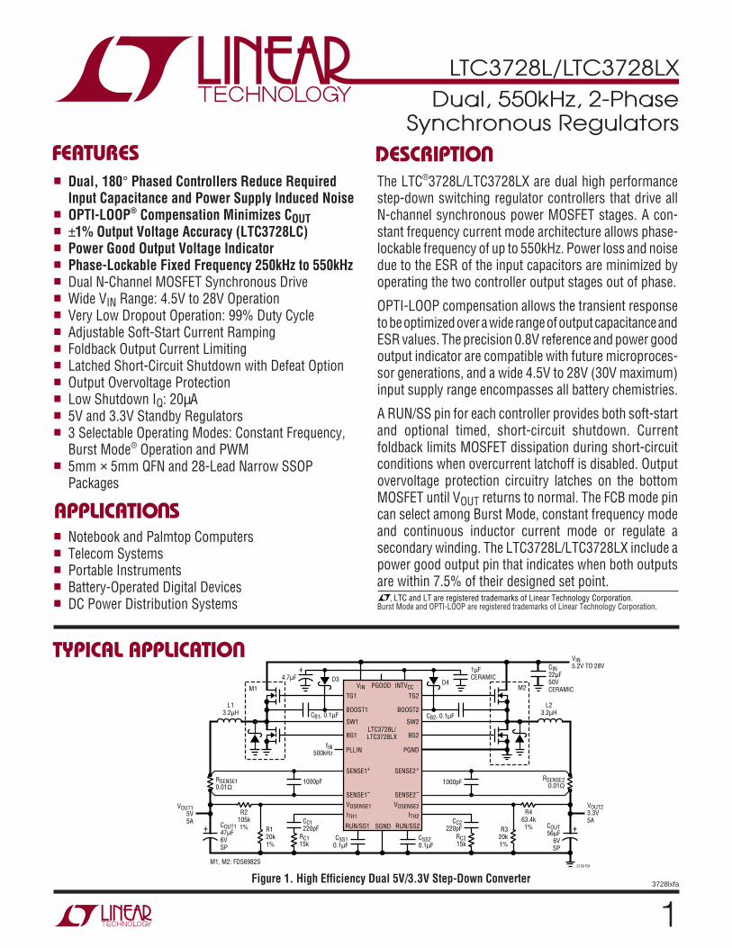
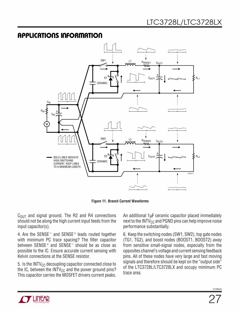
1 LTC3728L/LTC3728LX 3728lxfa Figure 1. High Efficiency Dual 5V/3.3V Step-Down Converter ■ Dual, 180° Phased Controllers Reduce Required Input Capacitance and Power Supply Induced Noise ■ OPTI-LOOP ® Compensation Minimizes C OUT ■ ±1% Output Voltage Accuracy (LTC3728LC) ■ Power Good Output Voltage Indicator ■ Phase-Lockable Fixed Frequency 250kHz to 550kHz ■ Dual N-Channel MOSFET Synchronous Drive ■ Wide V IN Range: 4.5V to 28V Operation ■ Very Low Dropout Operation: 99% Duty Cycle ■ Adjustable Soft-Start Current Ramping ■ Foldback Output Current Limiting ■ Latched Short-Circuit Shutdown with Defeat Option ■ Output Overvoltage Protection ■ Low Shutdown I Q : 20μ A ■ 5V and 3.3V Standby Regulators ■ 3 Selectable Operating Modes: Constant Frequency, Burst Mode ® Operation and PWM ■ 5mm × 5mm QFN and 28-Lead Narrow SSOP Packages The LTC ® 3728L/LTC3728LX are dual high performance step-down switching regulator controllers that drive all N-channel synchronous power MOSFET stages. A con- stant frequency current mode architecture allows phase- lockable frequency of up to 550kHz. Power loss and noise due to the ESR of the input capacitors are minimized by operating the two controller output stages out of phase. OPTI-LOOP compensation allows the transient response to be optimized over a wide range of output capacitance and ESR values. The precision 0.8V reference and power good output indicator are compatible with future microproces- sor generations, and a wide 4.5V to 28V (30V maximum) input supply range encompasses all battery chemistries. A RUN/SS pin for each controller provides both soft-start and optional timed, short-circuit shutdown. Current foldback limits MOSFET dissipation during short-circuit conditions when overcurrent latchoff is disabled. Output overvoltage protection circuitry latches on the bottom MOSFET until V OUT returns to normal. The FCB mode pin can select among Burst Mode, constant frequency mode and continuous inductor current mode or regulate a secondary winding. The LTC3728L/LTC3728LX include a power good output pin that indicates when both outputs are within 7.5% of their designed set point. ■ Notebook and Palmtop Computers ■ Telecom Systems ■ Portable Instruments ■ Battery-Operated Digital Devices ■ DC Power Distribution Systems , LTC and LT are registered trademarks of Linear Technology Corporation. Burst Mode and OPTI-LOOP are registered trademarks of Linear Technology Corporation. + 4.7μF D3 D4 M1 C B1 , 0.1μF R2 105k 1% 1000pF L1 3.2μH C C1 220pF 1μF CERAMIC C IN 22μF 50V CERAMIC + C OUT1 47μF 6V SP R SENSE1 0.01Ω R1 20k 1% R C1 15k V OUT1 5V 5A M2 C B2 , 0.1μF R4 63.4k 1% L2 3.2μH C C2 220pF 1000pF + C OUT 56μF 6V SP R SENSE2 0.01Ω R3 20k 1% R C2 15k V OUT2 3.3V 5A TG1 TG2 BOOST1 BOOST2 SW1 SW2 BG1 BG2 SGND PGND SENSE1 + SENSE2 + SENSE1 – SENSE2 – V OSENSE1 V OSENSE2 I TH1 I TH2 V IN PGOOD INTV CC RUN/SS1 RUN/SS2 V IN 5.2V TO 28V M1, M2: FDS6982S 3728 F01 C SS1 0.1μF C SS2 0.1μF LTC3728L/ LTC3728LX PLLIN f IN 500kHz FEATURES DESCRIPTIO U APPLICATIO S U TYPICAL APPLICATIO U Dual, 550kHz, 2-Phase Synchronous Regulators
Transcript
1
LTC3728L/LTC3728LX
3728lxfaFigure 1. High Efficiency Dual 5V/3.3V Step-Down Converter
Dual, 180° Phased Controllers Reduce RequiredInput Capacitance and Power Supply Induced Noise
OPTI-LOOP® Compensation Minimizes COUT ±1% Output Voltage Accuracy (LTC3728LC) Power Good Output Voltage Indicator Phase-Lockable Fixed Frequency 250kHz to 550kHz Dual N-Channel MOSFET Synchronous Drive Wide VIN Range: 4.5V to 28V Operation Very Low Dropout Operation: 99% Duty Cycle Adjustable Soft-Start Current Ramping Foldback Output Current Limiting Latched Short-Circuit Shutdown with Defeat Option Output Overvoltage Protection Low Shutdown IQ: 20µA 5V and 3.3V Standby Regulators 3 Selectable Operating Modes: Constant Frequency,
Burst Mode® Operation and PWM 5mm × 5mm QFN and 28-Lead Narrow SSOP
Packages
The LTC®3728L/LTC3728LX are dual high performancestep-down switching regulator controllers that drive allN-channel synchronous power MOSFET stages. A con-stant frequency current mode architecture allows phase-lockable frequency of up to 550kHz. Power loss and noisedue to the ESR of the input capacitors are minimized byoperating the two controller output stages out of phase.
OPTI-LOOP compensation allows the transient responseto be optimized over a wide range of output capacitance andESR values. The precision 0.8V reference and power goodoutput indicator are compatible with future microproces-sor generations, and a wide 4.5V to 28V (30V maximum)input supply range encompasses all battery chemistries.
A RUN/SS pin for each controller provides both soft-startand optional timed, short-circuit shutdown. Currentfoldback limits MOSFET dissipation during short-circuitconditions when overcurrent latchoff is disabled. Outputovervoltage protection circuitry latches on the bottomMOSFET until VOUT returns to normal. The FCB mode pincan select among Burst Mode, constant frequency modeand continuous inductor current mode or regulate asecondary winding. The LTC3728L/LTC3728LX include apower good output pin that indicates when both outputsare within 7.5% of their designed set point.
Notebook and Palmtop Computers Telecom Systems Portable Instruments Battery-Operated Digital Devices DC Power Distribution Systems , LTC and LT are registered trademarks of Linear Technology Corporation.
Burst Mode and OPTI-LOOP are registered trademarks of Linear Technology Corporation.
+4.7µF D3 D4
M1
CB1, 0.1µF
R2105k1%
1000pF
L13.2µH
CC1220pF
1µFCERAMIC
CIN22µF50VCERAMIC
+ COUT147µF6VSP
RSENSE10.01Ω
R120k1%
RC115k
VOUT15V5A
M2
CB2, 0.1µF
R463.4k1%
L23.2µH
CC2220pF
1000pF
+COUT56µF
6VSP
RSENSE20.01Ω
R320k1%
RC215k
VOUT23.3V5A
TG1 TG2
BOOST1 BOOST2
SW1 SW2
BG1 BG2
SGND
PGND
SENSE1+ SENSE2+
SENSE1– SENSE2–
VOSENSE1 VOSENSE2
ITH1 ITH2
VIN PGOOD INTVCC
RUN/SS1 RUN/SS2
VIN5.2V TO 28V
M1, M2: FDS6982S3728 F01
CSS10.1µF
CSS20.1µF
LTC3728L/LTC3728LX
PLLINfIN
500kHz
FEATURES DESCRIPTIO
U
APPLICATIO SU
TYPICAL APPLICATIO
U
Dual, 550kHz, 2-PhaseSynchronous Regulators
2
LTC3728L/LTC3728LX
3728lxfa
Input Supply Voltage (VIN) ........................ 30V to –0.3VTop Side Driver Voltages(BOOST1, BOOST2) .................................. 36V to –0.3VSwitch Voltage (SW1, SW2) ........................ 30V to –5VINTVCC, EXTVCC, RUN/SS1, RUN/SS2, (BOOST1-SW1),(BOOST2-SW2), PGOOD ............................ 7V to –0.3VSENSE1+, SENSE2 +, SENSE1–,SENSE2 – Voltages ....................... (1.1)INTVCC to –0.3VPLLIN, PLLFLTR, FCB, Voltage ........... INTVCC to –0.3V
ABSOLUTE AXI U RATI GS
W WW U
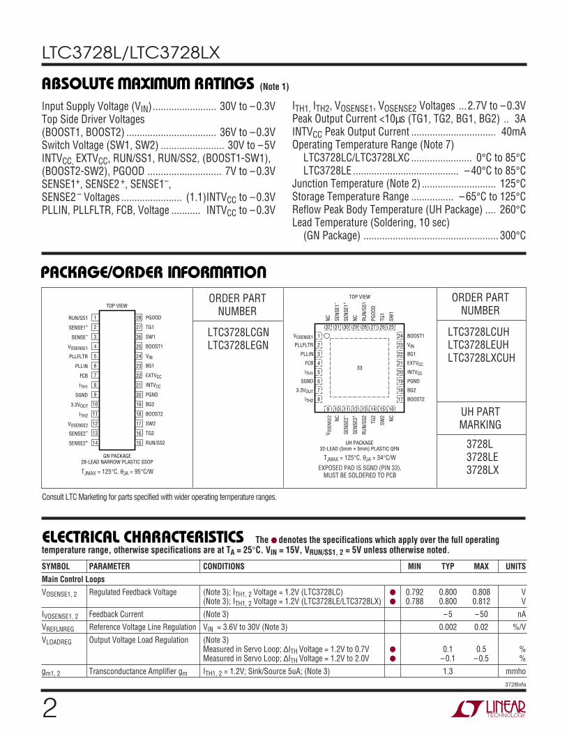
PACKAGE/ORDER I FOR ATIOU UW
(Note 1)
ITH1, ITH2, VOSENSE1, VOSENSE2 Voltages ...2.7V to –0.3VPeak Output Current <10µs (TG1, TG2, BG1, BG2) .. 3AINTVCC Peak Output Current ................................ 40mAOperating Temperature Range (Note 7)
LTC3728LC/LTC3728LXC ....................... 0°C to 85°CLTC3728LE ........................................ –40°C to 85°C
Junction Temperature (Note 2) ............................ 125°CStorage Temperature Range ................ – 65°C to 125°CReflow Peak Body Temperature (UH Package) .... 260°CLead Temperature (Soldering, 10 sec)
EXPOSED PAD IS SGND (PIN 33),MUST BE SOLDERED TO PCB
The denotes the specifications which apply over the full operatingtemperature range, otherwise specifications are at TA = 25°C. VIN = 15V, VRUN/SS1, 2 = 5V unless otherwise noted.ELECTRICAL CHARACTERISTICS
SYMBOL PARAMETER CONDITIONS MIN TYP MAX UNITSMain Control LoopsVOSENSE1, 2 Regulated Feedback Voltage (Note 3); ITH1, 2 Voltage = 1.2V (LTC3728LC) 0.792 0.800 0.808 V
(Note 3); ITH1, 2 Voltage = 1.2V (LTC3728LE/LTC3728LX) 0.788 0.800 0.812 VIVOSENSE1, 2 Feedback Current (Note 3) –5 – 50 nAVREFLNREG Reference Voltage Line Regulation VIN = 3.6V to 30V (Note 3) 0.002 0.02 %/VVLOADREG Output Voltage Load Regulation (Note 3)
Measured in Servo Loop; ∆ITH Voltage = 1.2V to 0.7V 0.1 0.5 %Measured in Servo Loop; ∆ITH Voltage = 1.2V to 2.0V –0.1 –0.5 %
Consult LTC Marketing for parts specified with wider operating temperature ranges.
UH PARTMARKING
3728L3728LE3728LX
ORDER PARTNUMBER
LTC3728LCGNLTC3728LEGN
1
2
3
4
5
6
7
8
9
10
11
12
13
14
TOP VIEW
GN PACKAGE28-LEAD NARROW PLASTIC SSOP
28
27
26
25
24
23
22
21
20
19
18
17
16
15
RUN/SS1
SENSE1+
SENSE–
VOSENSE1
PLLFLTR
PLLIN
FCB
ITH1
SGND
3.3VOUT
ITH2
VOSENSE2
SENSE2–
SENSE2+
PGOOD
TG1
SW1
BOOST1
VIN
BG1
EXTVCC
INTVCC
PGND
BG2
BOOST2
SW2
TG2
RUN/SS2
TJMAX = 125°C, θJA = 95°C/W
3
LTC3728L/LTC3728LX
3728lxfa
The denotes the specifications which apply over the full operatingtemperature range, otherwise specifications are at TA = 25°C. VIN = 15V, VRUN/SS1, 2 = 5V unless otherwise noted.ELECTRICAL CHARACTERISTICS
SYMBOL PARAMETER CONDITIONS MIN TYP MAX UNITSgmGBW1, 2 Transconductance Amplifier GBW ITH1, 2 = 1.2V; (Note 3) 3 MHzIQ Input DC Supply Current (Note 4)
TG1, 2 tr Rise Time CLOAD = 3300pF 55 100 nsTG1, 2 tf Fall Time CLOAD = 3300pF 55 100 ns
BG Transition Time: (Note 5)BG1, 2 tr Rise Time CLOAD = 3300pF 45 100 nsBG1, 2 tf Fall Time CLOAD = 3300pF 45 90 nsTG/BG t1D Top Gate Off to Bottom Gate On Delay
Synchronous Switch-On Delay Time CLOAD = 3300pF Each Driver 80 nsBG/TG t2D Bottom Gate Off to Top Gate On Delay
Top Switch-On Delay Time CLOAD = 3300pF Each Driver 80 nstON(MIN) Minimum On-Time Tested with a Square Wave (Note 6) 100 nsINTVCC Linear RegulatorVINTVCC Internal VCC Voltage 6V < VIN < 30V, VEXTVCC = 4V 4.8 5.0 5.2 VVLDO INT INTVCC Load Regulation ICC = 0 to 20mA, VEXTVCC = 4V 0.2 2.0 %VLDO EXT EXTVCC Voltage Drop ICC = 20mA, VEXTVCC = 5V 100 200 mVVEXTVCC EXTVCC Switchover Voltage ICC = 20mA, EXTVCC Ramping Positive 4.5 4.7 VVLDOHYS EXTVCC Hysteresis 0.2 VOscillator and Phase-Locked LoopfNOM Nominal Frequency VPLLFLTR = 1.2V 360 400 440 kHzfLOW Lowest Frequency VPLLFLTR = 0V 230 260 290 kHzfHIGH Highest Frequency VPLLFLTR ≥ 2.4V 480 550 590 kHzRPLLIN PLLIN Input Resistance 50 kΩIPLLFLTR Phase Detector Output Current
Note 1: Absolute Maximum Ratings are those values beyond which the lifeof a device may be impaired.Note 2: TJ is calculated from the ambient temperature TA and powerdissipation PD according to the following formulas:
LTC3728LUH/LTC3728LXUH: TJ = TA + (PD • 34°C/W)LTC3728LGN: TJ = TA + (PD • 95°C/W)
Note 3: The IC is tested in a feedback loop that servos VITH1, 2 to aspecified voltage and measures the resultant VOSENSE1, 2.
Note 4: Dynamic supply current is higher due to the gate charge being
delivered at the switching frequency. See Applications Information.Note 5: Rise and fall times are measured using 10% and 90% levels. Delaytimes are measured using 50% levels.Note 6: The minimum on-time condition is specified for an inductorpeak-to-peak ripple current ≥40% of IMAX (see minimum on-timeconsiderations in the Applications Information section).Note 7: The LTC3728LC/LTC3728LXC are guaranteed to meetperformance specifications from 0°C to 85°C. The LTC3728LE isguaranteed to meet performance specifications over the –40°C to 85°Coperating temperature range as assured by design, characterization andcorrelation with statistical process controls.
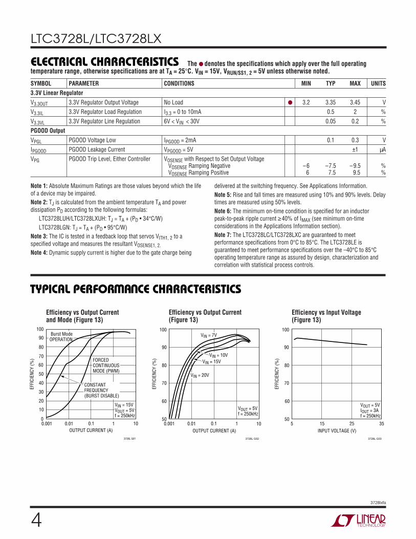
Efficiency vs Output Currentand Mode (Figure 13)
OUTPUT CURRENT (A)0.0010
EFFI
CIEN
CY (%
)
10
30
40
50
100
70
0.01 0.1 1
3728L G01
20
80
90
60
10
FORCEDCONTINUOUSMODE (PWM)
CONSTANTFREQUENCY(BURST DISABLE)
Burst ModeOPERATION
VIN = 15VVOUT = 5Vf = 250kHz
OUTPUT CURRENT (A)0.001
EFFI
CIEN
CY (%
)
70
80
10
3728L G02
60
500.01 0.1 1
100
90
VIN = 10VVIN = 15V
VIN = 7V
VIN = 20V
VOUT = 5Vf = 250kHz
INPUT VOLTAGE (V)5
EFFI
CIEN
CY (%
)
70
80
3728L G03
60
5015 25 35
100
VOUT = 5VIOUT = 3Af = 250kHz
90
Efficiency vs Output Current(Figure 13)
Efficiency vs Input Voltage(Figure 13)
TYPICAL PERFOR A CE CHARACTERISTICS
UW
The denotes the specifications which apply over the full operatingtemperature range, otherwise specifications are at TA = 25°C. VIN = 15V, VRUN/SS1, 2 = 5V unless otherwise noted.ELECTRICAL CHARACTERISTICS
SYMBOL PARAMETER CONDITIONS MIN TYP MAX UNITS3.3V Linear RegulatorV3.3OUT 3.3V Regulator Output Voltage No Load 3.2 3.35 3.45 VV3.3IL 3.3V Regulator Load Regulation I3.3 = 0 to 10mA 0.5 2 %V3.3VL 3.3V Regulator Line Regulation 6V < VIN < 30V 0.05 0.2 %PGOOD OutputVPGL PGOOD Voltage Low IPGOOD = 2mA 0.1 0.3 VIPGOOD PGOOD Leakage Current VPGOOD = 5V ±1 µAVPG PGOOD Trip Level, Either Controller VOSENSE with Respect to Set Output Voltage
Constant Frequency (Burst Inhibit)Operation (Figure 13)
VOUT20mV/DIV
IL0.5A/DIV
VIN = 15V 2µs/DIV 3728L G24
VOUT = 5VVPLLFLTR = 0VVFCB = 5VIOUT = 20mA
VSW210V/DIV
8
LTC3728L/LTC3728LX
3728lxfa
VOSENSE1, VOSENSE2: Error Amplifier Feedback Input. Re-ceives the remotely-sensed feedback voltage for eachcontroller from an external resistive divider across theoutput.
PLLFLTR: Filter Connection for Phase-Locked Loop. Al-ternatively, this pin can be driven with an AC or DC voltagesource to vary the frequency of the internal oscillator.
PLLIN: External Synchronization Input to Phase Detector.This pin is internally terminated to SGND with 50kΩ. Thephase-locked loop will force the rising top gate signal ofcontroller 1 to be synchronized with the rising edge of thePLLIN signal.
FCB: Forced Continuous Control Input. This input acts onboth controllers and is normally used to regulate asecondary winding. Pulling this pin below 0.8V will forcecontinuous synchronous operation.
ITH1, ITH2: Error Amplifier Output and Switching RegulatorCompensation Point. Each associated channels’ currentcomparator trip point increases with this control voltage.
SGND: Small Signal Ground. Common to both con-trollers, this pin must be routed separately from highcurrent grounds to the common (–) terminals of theCOUT capacitors.
3.3VOUT: Lnear Regulator Output. Capable of supplying10mA DC with peak currents as high as 50mA.
NC: No Connect.
SENSE2–, SENSE1–: The (–) Input to the DifferentialCurrent Comparators.
SENSE2+, SENSE1+: The (+) Input to the DifferentialCurrent Comparators. The ITH pin voltage and controlledoffsets between the SENSE– and SENSE+ pins in conjunc-tion with RSENSE set the current trip threshold.
RUN/SS2, RUN/SS1: Combination of soft-start, run con-trol inputs and short-circuit detection timers. A capacitorto ground at each of these pins sets the ramp time to fulloutput current. Forcing either of these pins back below1.0V causes the IC to shut down the circuitry required forthat particular controller. Latchoff overcurrent protection
is also invoked via this pin as described in the ApplicationsInformation section.
TG2, TG1: High Current Gate Drives for Top N-ChannelMOSFETs. These are the outputs of floating drivers with avoltage swing equal to INTVCC – 0.5V superimposed onthe switch node voltage SW.
SW2, SW1: Switch Node Connections to Inductors. Volt-age swing at these pins is from a Schottky diode (external)voltage drop below ground to VIN.
BOOST2, BOOST1: Bootstrapped Supplies to the Top SideFloating Drivers. Capacitors are connected between theboost and switch pins and Schottky diodes are tied be-tween the boost and INTVCC pins. Voltage swing at theboost pins is from INTVCC to (VIN + INTVCC).
BG2, BG1: High Current Gate Drives for Bottom (Synchro-nous) N-Channel MOSFETs. Voltage swing at these pins isfrom ground to INTVCC.
PGND: Driver Power Ground. Connects to the sources ofbottom (synchronous) N-channel MOSFETs, anodes of theSchottky rectifiers and the (–) terminal(s) of CIN.
INTVCC: Output of the Internal 5V Linear Low DropoutRegulator and the EXTVCC Switch. The driver and controlcircuits are powered from this voltage source. Must bedecoupled to power ground with a minimum of 4.7µF tanta-lum or other low ESR capacitor.
EXTVCC: External Power Input to an Internal Switch Con-nected to INTVCC. This switch closes and supplies VCCpower, bypassing the internal low dropout regulator, when-ever EXTVCC is higher than 4.7V. See EXTVCC connectionin Applications section. Do not exceed 7V on this pin.
VIN: Main Supply Pin. A bypass capacitor should be tiedbetween this pin and the signal ground pin.
PGOOD: Open-Drain Logic Output. PGOOD is pulled toground when the voltage on either VOSENSE pin is notwithin ±7.5% of its set point.
Exposed Pad (UH Package Only): Signal Ground. Must besoldered to the PCB, providing a local ground for thecontrol components of the IC, and be tied to the PGND pinunder the IC.
UUU
PI FU CTIO S
9
LTC3728L/LTC3728LX
3728lxfa
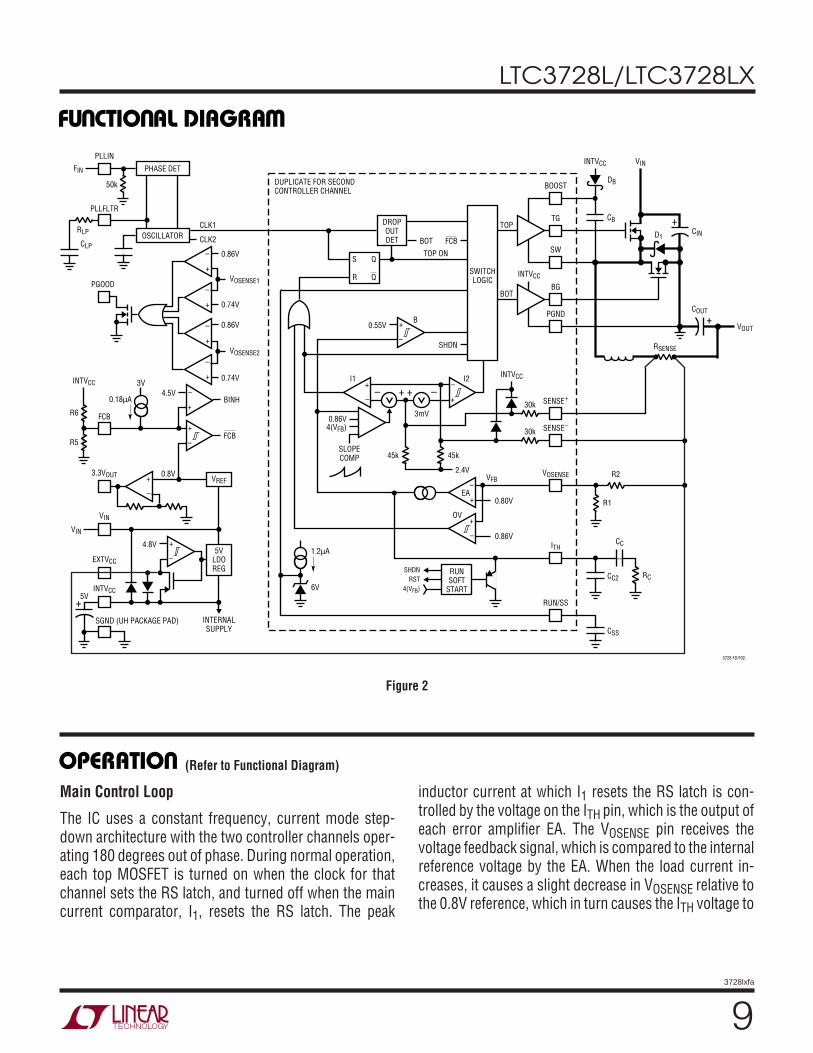
Figure 2
FU CTIO AL DIAGRA
UU W
(Refer to Functional Diagram)OPERATIOU
Main Control Loop
The IC uses a constant frequency, current mode step-down architecture with the two controller channels oper-ating 180 degrees out of phase. During normal operation,each top MOSFET is turned on when the clock for thatchannel sets the RS latch, and turned off when the maincurrent comparator, I1, resets the RS latch. The peak
inductor current at which I1 resets the RS latch is con-trolled by the voltage on the ITH pin, which is the output ofeach error amplifier EA. The VOSENSE pin receives thevoltage feedback signal, which is compared to the internalreference voltage by the EA. When the load current in-creases, it causes a slight decrease in VOSENSE relative tothe 0.8V reference, which in turn causes the ITH voltage to
SWITCHLOGIC
–
+
0.8V
4.8V
5V
VIN
VIN
4.5VBINH
CLK2
CLK1
0.18µA
R6
R5
+
–
FCB
+
–
–
+
–
+
–
+ VREF
INTERNALSUPPLY
3.3VOUT
INTVCC
RLP
CLP
3V
FCB
EXTVCC
INTVCC
SGND (UH PACKAGE PAD)
+
5VLDOREG
SW
SHDN
0.55V
TOP
BOOST
TG CB
CIND1
DB
PGND
BOTBG
INTVCC
INTVCC
VIN
+
COUT
VOUT
3728 FD/F02
RSENSE
R2
+
VOSENSE
DROPOUTDET
RUNSOFT
START
BOT
TOP ONS
R
Q
Q
OSCILLATOR
PHASE DET
PLLFLTR
PLLIN
FCB
EA
0.86V
0.80V
OV
VFB
1.2µA
6V
R1
–
+
RC
4(VFB)RST
SHDN
RUN/SS
ITHCC
CC2
CSS
4(VFB)0.86V
SLOPECOMP
3mV
+
–
–
+
SENSE–
SENSE+
INTVCC
30k
45k
2.4V
45k
30k
I1 I2
B
DUPLICATE FOR SECONDCONTROLLER CHANNEL
+– –+
50k
FIN
+
–
+
–
+
–
+
–
PGOODVOSENSE1
VOSENSE2
0.86V
0.74V
0.86V
0.74V
10
LTC3728L/LTC3728LX
3728lxfa
(Refer to Functional Diagram)
increase until the average inductor current matches thenew load current. After the top MOSFET has turned off, thebottom MOSFET is turned on until either the inductorcurrent starts to reverse, as indicated by current compara-tor I2, or the beginning of the next cycle.
The top MOSFET drivers are biased from floating boot-strap capacitor CB, which normally is recharged duringeach off cycle through an external diode when the topMOSFET turns off. As VIN decreases to a voltage close toVOUT, the loop may enter dropout and attempt to turn onthe top MOSFET continuously. The dropout detector de-tects this and forces the top MOSFET off for about 400nsevery tenth cycle to allow CB to recharge.
The main control loop is shut down by pulling the RUN/SSpin low. Releasing RUN/SS allows an internal 1.2µAcurrent source to charge soft-start capacitor CSS. WhenCSS reaches 1.5V, the main control loop is enabled with theITH voltage clamped at approximately 30% of its maximumvalue. As CSS continues to charge, the ITH pin voltage isgradually released allowing normal, full-current opera-tion. When both RUN/SS1 and RUN/SS2 are low, allcontroller functions are shut down, including the 5V and3.3V regulators.
Low Current Operation
The FCB pin is a multifunction pin providing two func-tions: 1) to provide regulation for a secondary winding bytemporarily forcing continuous PWM operation onboth controllers; and 2) to select between two modes oflow current operation. When the FCB pin voltage is below0.8V, the controller forces continuous PWM currentmode operation. In this mode, the top and bottomMOSFETs are alternately turned on to maintain the outputvoltage independent of direction of inductor current.When the FCB pin is below VINTVCC – 2V but greater than0.8V, the controller enters Burst Mode operation. BurstMode operation sets a minimum output current levelbefore inhibiting the top switch and turns off the synchro-nous MOSFET(s) when the inductor current goes nega-tive. This combination of requirements will, at low cur-rents, force the ITH pin below a voltage threshold that will
OPERATIOU
temporarily inhibit turn-on of both output MOSFETs untilthe output voltage drops. There is 60mV of hysteresis inthe burst comparator B tied to the ITH pin. This hysteresisproduces output signals to the MOSFETs that turn themon for several cycles, followed by a variable “sleep”interval depending upon the load current. The resultantoutput voltage ripple is held to a very small value byhaving the hysteretic comparator after the error amplifiergain block.
Frequency Synchronization
The phase-locked loop allows the internal oscillator to besynchronized to an external source via the PLLIN pin. Theoutput of the phase detector at the PLLFLTR pin is also theDC frequency control input of the oscillator that operatesover a 260kHz to 550kHz range corresponding to a DCvoltage input from 0V to 2.4V. When locked, the PLL alignsthe turn on of the top MOSFET to the rising edge of thesynchronizing signal. When PLLIN is left open, the PLLFLTRpin goes low, forcing the oscillator to minimum frequency.
Constant Frequency Operation
When the FCB pin is tied to INTVCC, Burst Mode operationis disabled and the forced minimum output currentrequirement is removed. This provides constant frequency,discontinuous current (preventing reverse inductor cur-rent) operation over the widest possible output currentrange. This constant frequency operation is not as efficientas Burst Mode operation, but does provide a lower noise,constant frequency operating mode down to approxi-mately 1% of the designed maximum output current.
Continuous Current (PWM) Operation
Tying the FCB pin to ground will force continuous currentoperation. This is the least efficient operating mode, butmay be desirable in certain applications. The output cansource or sink current in this mode. When sinking currentwhile in forced continuous operation, current will beforced back into the main power supply potentially boost-ing the input supply to dangerous voltage levels—BEWARE!
11
LTC3728L/LTC3728LX
3728lxfa
INTVCC/EXTVCC Power
Power for the top and bottom MOSFET drivers and mostother internal circuitry is derived from the INTVCC pin.When the EXTVCC pin is left open, an internal 5V lowdropout linear regulator supplies INTVCC power. If EXTVCCis taken above 4.7V, the 5V regulator is turned off and aninternal switch is turned on connecting EXTVCC to INTVCC.This allows the INTVCC power to be derived from a highefficiency external source such as the output of the regu-lator itself or a secondary winding, as described in theApplications Information section.
Output Overvoltage Protection
An overvoltage comparator, OV, guards against transientovershoots (>7.5%) as well as other more serious condi-tions that may overvoltage the output. In this case, the topMOSFET is turned off and the bottom MOSFET is turned onuntil the overvoltage condition is cleared.
Power Good (PGOOD) Pin
The PGOOD pin is connected to an open drain of an internalMOSFET. The MOSFET turns on and pulls the pin low wheneither output is not within ±7.5% of the nominal outputlevel as determined by the resistive feedback divider.When both outputs meet the ±7.5% requirement, theMOSFET is turned off within 10µs and the pin is allowed tobe pulled up by an external resistor to a source of up to 7V.
The RUN/SS capacitors are used initially to limit the inrushcurrent of each switching regulator. After the controllerhas been started and been given adequate time to chargeup the output capacitors and provide full load current, theRUN/SS capacitor is used in a short-circuit time-outcircuit. If the output voltage falls to less than 70% of itsnominal output voltage, the RUN/SS capacitor beginsdischarging on the assumption that the output is in anovercurrent and/or short-circuit condition. If the condi-tion lasts for a long enough period as determined by thesize of the RUN/SS capacitor, the controller will be shutdown until the RUN/SS pin(s) voltage(s) are recycled.
This built-in latchoff can be overridden by providing a>5µA pull-up at a compliance of 5V to the RUN/SS pin(s).This current shortens the soft start period but also pre-vents net discharge of the RUN/SS capacitor(s) during anovercurrent and/or short-circuit condition. Foldback cur-rent limiting is also activated when the output voltage fallsbelow 70% of its nominal level whether or not the short-circuit latchoff circuit is enabled. Even if a short is presentand the short-circuit latchoff is not enabled, a safe, lowoutput current is provided due to internal current foldbackand actual power wasted is low due to the efficient natureof the current mode switching regulator.
THEORY AND BENEFITS OF 2-PHASE OPERATION
The LTC1628 and the LTC3728L family of dual highefficiency DC/DC controllers brings the considerable ben-efits of 2-phase operation to portable applications for thefirst time. Notebook computers, PDAs, handheld termi-nals and automotive electronics will all benefit from thelower input filtering requirement, reduced electromag-netic interference (EMI) and increased efficiency associ-ated with 2-phase operation.
Why the need for 2-phase operation? Up until the 2-phasefamily, constant-frequency dual switching regulators op-erated both channels in phase (i.e., single-phase opera-tion). This means that both switches turned on at the sametime, causing current pulses of up to twice the amplitudeof those for one regulator to be drawn from the inputcapacitor and battery. These large amplitude current pulsesincreased the total RMS current flowing from the inputcapacitor, requiring the use of more expensive inputcapacitors and increasing both EMI and losses in the inputcapacitor and battery.
With 2-phase operation, the two channels of the dual-switching regulator are operated 180 degrees out ofphase. This effectively interleaves the current pulsesdrawn by the switches, greatly reducing the overlap timewhere they add together. The result is a significant reduc-tion in total RMS input current, which in turn allows lessexpensive input capacitors to be used, reduces shieldingrequirements for EMI and improves real world operatingefficiency.
(Refer to Functional Diagram)OPERATIOU
12
LTC3728L/LTC3728LX
3728lxfa
Figure 3 compares the input waveforms for a representa-tive single-phase dual switching regulator to the LTC16282-phase dual switching regulator. An actual measurementof the RMS input current under these conditions showsthat 2-phase operation dropped the input current from2.53ARMS to 1.55ARMS. While this is an impressive reduc-tion in itself, remember that the power losses are propor-tional to IRMS
2, meaning that the actual power wasted isreduced by a factor of 2.66. The reduced input ripplevoltage also means less power is lost in the input powerpath, which could include batteries, switches, trace/con-nector resistances and protection circuitry. Improvementsin both conducted and radiated EMI also directly accrue asa result of the reduced RMS input current and voltage.
Of course, the improvement afforded by 2-phase opera-tion is a function of the dual switching regulator’s relativeduty cycles which, in turn, are dependent upon the inputvoltage VIN (Duty Cycle = VOUT/VIN). Figure 4 shows howthe RMS input current varies for single-phase and 2-phaseoperation for 3.3V and 5V regulators over a wide inputvoltage range.
It can readily be seen that the advantages of 2-phaseoperation are not just limited to a narrow operating range,but in fact extend over a wide region. A good rule of thumbfor most applications is that 2-phase operation will reducethe input capacitor requirement to that for just one channeloperating at maximum current and 50% duty cycle.
A final question: If 2-phase operation offers such anadvantage over single-phase operation for dual switching
regulators, why hasn’t it been done before? The answer isthat, while simple in concept, it is hard to implement.Constant-frequency current mode switching regulatorsrequire an oscillator derived “slope compensation” signalto allow stable operation of each regulator at over 50%duty cycle. This signal is relatively easy to derive in single-phase dual switching regulators, but required the develop-ment of a new and proprietary technique to allow 2-phaseoperation. In addition, isolation between the two channelsbecomes more critical with 2-phase operation becauseswitch transitions in one channel could potentially disruptthe operation of the other channel.
These 2-phase parts are proof that these hurdles havebeen surmounted. They offer unique advantages for theever-expanding number of high efficiency power suppliesrequired in portable electronics.
Figure 3. Input Waveforms Comparing Single-Phase (a) and 2-Phase (b) Operation for Dual Switching RegulatorsConverting 12V to 5V and 3.3V at 3A Each. The Reduced Input Ripple with the LTC1628 2-Phase Regulator AllowsLess Expensive Input Capacitors, Reduces Shielding Requirements for EMI and Improves Efficiency
(Refer to Functional Diagram)OPERATIOU
Figure 4. RMS Input Current Comparison
INPUT VOLTAGE (V)0
INPU
T RM
S CU
RREN
T (A
)
3.0
2.5
2.0
1.5
1.0
0.5
010 20 30 40
3728 F04
SINGLE PHASEDUAL CONTROLLER
2-PHASEDUAL CONTROLLER
VO1 = 5V/3AVO2 = 3.3V/3A
13
LTC3728L/LTC3728LX
3728lxfa
Figure 1 on the first page is a basic LTC3728L/LTC3728LXapplication circuit. External component selection is drivenby the load requirement, and begins with the selection ofRSENSE and the inductor value. Next, the power MOSFETsand D1 are selected. Finally, CIN and COUT are selected.The circuit shown in Figure 1 can be configured foroperation up to an input voltage of 28V (limited by theexternal MOSFETs).
RSENSE Selection For Output Current
RSENSE is chosen based on the required output current.The current comparator has a maximum threshold of75mV/RSENSE and an input common mode range of SGNDto 1.1(INTVCC). The current comparator threshold sets thepeak of the inductor current, yielding a maximum averageoutput current IMAX equal to the peak value less half thepeak-to-peak ripple current, ∆IL.
Allowing a margin for variations in the IC and externalcomponent values yields:
RmV
ISENSE
MAX= 50
When using the controller in very low dropout conditions,the maximum output current level will be reduced due tothe internal compensation required to meet stability crite-rion for buck regulators operating at greater than 50%duty factor. A curve is provided to estimate this reductionin peak output current level depending upon the operatingduty factor.
Operating Frequency
The IC uses a constant frequency phase-lockable architec-ture with the frequency determined by an internal capaci-tor. This capacitor is charged by a fixed current plus anadditional current which is proportional to the voltageapplied to the PLLFLTR pin. Refer to Phase-Locked Loopand Frequency Synchronization in the Applications Infor-mation section for additional information.
A graph for the voltage applied to the PLLFLTR pin vsfrequency is given in Figure 5. As the operating frequency
is increased the gate charge losses will be higher, reducingefficiency (see Efficiency Considerations). The maximumswitching frequency is approximately 550kHz.
Inductor Value Calculation
The operating frequency and inductor selection are inter-related in that higher operating frequencies allow the useof smaller inductor and capacitor values. So why wouldanyone ever choose to operate at lower frequencies withlarger components? The answer is efficiency. A higherfrequency generally results in lower efficiency because ofMOSFET gate charge losses. In addition to this basictrade-off, the effect of inductor value on ripple current andlow current operation must also be considered.
The inductor value has a direct effect on ripple current. Theinductor ripple current ∆IL decreases with higher induc-tance or frequency and increases with higher VIN:
∆If L
VVV
L OUTOUT
IN=
1
1( )( )
–
Accepting larger values of ∆IL allows the use of lowinductances, but results in higher output voltage rippleand greater core losses. A reasonable starting point forsetting ripple current is ∆IL=0.3(IMAX). The maximum ∆ILoccurs at the maximum input voltage.
APPLICATIO S I FOR ATIO
WU UU
Figure 5. PLLFLTR Pin Voltage vs Frequency
OPERATING FREQUENCY (kHz)200 300 400 500 600
PLLF
LTR
PIN
VOLT
AGE
(V)
3728 F05
2.5
2.0
1.5
1.0
0.5
0
14
LTC3728L/LTC3728LX
3728lxfa
The inductor value also has secondary effects. The transi-tion to Burst Mode operation begins when the averageinductor current required results in a peak current below25% of the current limit determined by RSENSE. Lowerinductor values (higher ∆IL) will cause this to occur atlower load currents, which can cause a dip in efficiency inthe upper range of low current operation. In Burst Modeoperation, lower inductance values will cause the burstfrequency to decrease.
Inductor Core Selection
Once the value for L is known, the type of inductor mustbe selected. High efficiency converters generally cannotafford the core loss found in low cost powdered ironcores, forcing the use of more expensive ferrite, molyper-malloy, or Kool Mµ® cores. Actual core loss is indepen-dent of core size for a fixed inductor value, but it is verydependent on inductance selected. As inductance in-creases, core losses go down. Unfortunately, increasedinductance requires more turns of wire and thereforecopper losses will increase.
Ferrite designs have very low core loss and are preferredat high switching frequencies, so design goals can con-centrate on copper loss and preventing saturation. Ferritecore material saturates “hard,” which means that induc-tance collapses abruptly when the peak design current isexceeded. This results in an abrupt increase in inductorripple current and consequent output voltage ripple. Donot allow the core to saturate!
Molypermalloy (from Magnetics, Inc.) is a very good, lowloss core material for toroids, but it is more expensive thanferrite. A reasonable compromise from the same manu-facturer is Kool Mµ. Toroids are very space efficient,especially when you can use several layers of wire. Be-cause they generally lack a bobbin, mounting is moredifficult. However, designs for surface mount are availablethat do not increase the height significantly.
Power MOSFET and D1 Selection
Two external power MOSFETs must be selected for eachcontroller in the LTC3728L/LTC3728LX: One N-channelMOSFET for the top (main) switch, and one N-channelMOSFET for the bottom (synchronous) switch.
The peak-to-peak drive levels are set by the INTVCCvoltage. This voltage is typically 5V during start-up (seeEXTVCC Pin Connection). Consequently, logic-levelthreshold MOSFETs must be used in most applications.The only exception is if low input voltage is expected(VIN < 5V); then, sub-logic level threshold MOSFETs(VGS(TH) < 3V) should be used. Pay close attention to theBVDSS specification for the MOSFETs as well; most of thelogic level MOSFETs are limited to 30V or less.
Selection criteria for the power MOSFETs include the “ON”resistance RDS(ON), Miller capacitance CMILLER, input volt-age and maximum output current. Miller capacitance,CMILLER, can be approximated from the gate charge curveusually provided on the MOSFET manufacturers’ datasheet. CMILLER is equal to the increase in gate charge alongthe horizontal axis while the curve is approximately flatdivided by the specified change in VDS. This result is thenmultiplied by the ratio of the application applied VDS to theGate charge curve specified VDS. When the IC is operatingin continuous mode the duty cycles for the top and bottomMOSFETs are given by:
Main SwitchDuty CycleVVOUT
IN=
Synchronous SwitchDuty CycleV V
VIN OUT
IN= –
The MOSFET power dissipations at maximum outputcurrent are given by:
PVV
I R
VI
R C
V V Vf
MAINOUT
INMAX DS ON
INMAX
DR MILLER
INTVCC THMIN THMIN
= ( ) +( ) +
( )
( )( )
+
( )
2
2
1
2
1 1
δ ( )
•
–
PV V
VI RSYNC
IN OUT
INMAX DS ON= ( ) +( )–
( )2
1 δ
Kool Mµ is a registered trademark of Magnetics, Inc.
APPLICATIO S I FOR ATIO
WU UU
15
LTC3728L/LTC3728LX
3728lxfa
where δ is the temperature dependency of RDS(ON) andRDR (approximately 4Ω) is the effective driver resistanceat the MOSFET’s Miller threshold voltage. VTHMIN is thetypical MOSFET minimum threshold voltage.
Both MOSFETs have I2R losses while the topside N-channelequation includes an additional term for transition losses,which are highest at high input voltages. For VIN < 20V thehigh current efficiency generally improves with largerMOSFETs, while for VIN > 20V the transition losses rapidlyincrease to the point that the use of a higher RDS(ON) devicewith lower CMILLER actually provides higher efficiency. Thesynchronous MOSFET losses are greatest at high inputvoltage when the top switch duty factor is low or during ashort-circuit when the synchronous switch is on close to100% of the period.
The term (1+δ) is generally given for a MOSFET in the formof a normalized RDS(ON) vs Temperature curve, butδ = 0.005/°C can be used as an approximation for lowvoltage MOSFETs.
The Schottky diode D1 shown in Figure 1 conducts duringthe dead-time between the conduction of the two powerMOSFETs. This prevents the body diode of the bottomMOSFET from turning on, storing charge during the dead-time and requiring a reverse recovery period that couldcost as much as 3% in efficiency at high VIN. A 1A to 3ASchottky is generally a good compromise for both regionsof operation due to the relatively small average current.Larger diodes result in additional transition losses due totheir larger junction capacitance.
CIN and COUT Selection
The selection of CIN is simplified by the multiphase archi-tecture and its impact on the worst-case RMS currentdrawn through the input network (battery/fuse/capacitor).It can be shown that the worst case RMS current occurswhen only one controller is operating. The controller withthe highest (VOUT)(IOUT) product needs to be used in theformula below to determine the maximum RMS currentrequirement. Increasing the output current, drawn fromthe other out-of-phase controller, will actually decreasethe input RMS ripple current from this maximum value(see Figure 4). The out-of-phase technique typically re-duces the input capacitor’s RMS ripple current by a factor
of 30% to 70% when compared to a single phase powersupply solution.
The type of input capacitor, value and ESR rating haveefficiency effects that need to be considered in the selec-tion process. The capacitance value chosen should besufficient to store adequate charge to keep high peakbattery currents down. 20µF to 40µF is usually sufficientfor a 25W output supply operating at 200kHz. The ESR ofthe capacitor is important for capacitor power dissipationas well as overall battery efficiency. All of the power (RMSripple current • ESR) not only heats up the capacitor butwastes power from the battery.
Medium voltage (20V to 35V) ceramic, tantalum, OS-CONand switcher-rated electrolytic capacitors can be used asinput capacitors, but each has drawbacks: ceramic voltagecoefficients are very high and may have audible piezoelec-tric effects; tantalums need to be surge-rated; OS-CONssuffer from higher inductance, larger case size and limitedsurface-mount applicability; electrolytics’ higher ESR anddryout possibility require several to be used. Multiphasesystems allow the lowest amount of capacitance overall.As little as one 22µF or two to three 10µF ceramic capaci-tors are an ideal choice in a 20W to 35W power supply dueto their extremely low ESR. Even though the capacitanceat 20V is substantially below their rating at zero-bias, verylow ESR loss makes ceramics an ideal candidate forhighest efficiency battery operated systems. Also con-sider parallel ceramic and high quality electrolytic capaci-tors as an effective means of achieving ESR and bulkcapacitance goals.
In continuous mode, the source current of the top N-chan-nel MOSFET is a square wave of duty cycle VOUT/VIN. Toprevent large voltage transients, a low ESR input capacitorsized for the maximum RMS current of one channel mustbe used. The maximum RMS capacitor current is given by:
C quiredI IV V V
VIN RMS MAX
OUT IN OUT
INRe
/
≈−( )[ ]1 2
This formula has a maximum at VIN = 2VOUT, whereIRMS = IOUT/2. This simple worst case condition is com-monly used for design because even significant deviationsdo not offer much relief. Note that capacitor manufacturer’s
APPLICATIO S I FOR ATIO
WU UU
16
LTC3728L/LTC3728LX
3728lxfa
ripple current ratings are often based on only 2000 hoursof life. This makes it advisable to further derate thecapacitor, or to choose a capacitor rated at a highertemperature than required. Several capacitors may also beparalleled to meet size or height requirements in thedesign. Always consult the manufacturer if there is anyquestion.
The benefit of the LTC3728L/LTC3728LX multiphase clock-ing can be calculated by using the equation above for thehigher power controller and then calculating the loss thatwould have resulted if both controller channels switchedon at the same time. The total RMS power lost is lowerwhen both controllers are operating due to the interleavingof current pulses through the input capacitor’s ESR. Thisis why the input capacitor’s requirement calculated abovefor the worst-case controller is adequate for the dualcontroller design. Remember that input protection fuseresistance, battery resistance and PC board trace resis-tance losses are also reduced due to the reduced peakcurrents in a multiphase system. The overall benefit of amultiphase design will only be fully realized when thesource impedance of the power supply/battery is includedin the efficiency testing. The drains of the two top MOSFETSshould be placed within 1cm of each other and share acommon CIN(s). Separating the drains and CIN may pro-duce undesirable voltage and current resonances at VIN.
The selection of COUT is driven by the required effectiveseries resistance (ESR). Typically once the ESR require-ment is satisfied the capacitance is adequate for filtering.The output ripple (∆VOUT) is determined by:
∆ ∆V I ESRfC
OUT LOUT
≈ +
1
8
Where f = operating frequency, COUT = output capacitance,and ∆IL= ripple current in the inductor. The output rippleis highest at maximum input voltage since ∆IL increaseswith input voltage. With ∆IL = 0.3IOUT(MAX) the outputripple will typically be less than 50mV at the maximum VINassuming:
COUT Recommended ESR < 2 RSENSE
and COUT > 1/(8fRSENSE)
The first condition relates to the ripple current into theESR of the output capacitance while the second termguarantees that the output capacitance does not signifi-cantly discharge during the operating frequency perioddue to ripple current. The choice of using smaller outputcapacitance increases the ripple voltage due to the dis-charging term but can be compensated for by usingcapacitors of very low ESR to maintain the ripple voltageat or below 50mV. The ITH pin OPTI-LOOP compensationcomponents can be optimized to provide stable, highperformance transient response regardless of the outputcapacitors selected.
Manufacturers such as Nichicon, United Chemi-Con andSanyo can be considered for high performance through-hole capacitors. The OS-CON semiconductor dielectriccapacitor available from Sanyo has the lowest (ESR)(size)product of any aluminum electrolytic at a somewhathigher price. An additional ceramic capacitor in parallelwith OS-CON capacitors is recommended to reduce theinductance effects.
In surface mount applications multiple capacitors mayneed to be used in parallel to meet ESR, RMS currenthandling and load step requirements. Aluminum electro-lytic, dry tantalum and special polymer capacitors areavailable in surface mount packages. Special polymersurface mount capacitors offer very low ESR but havelower storage capacity per unit volume than other capaci-tor types. These capacitors offer a very cost-effectiveoutput capacitor solution and are an ideal choice whencombined with a controller having high loop bandwidth.Tantalum capacitors offer the highest capacitance densityand are often used as output capacitors for switchingregulators having controlled soft-start. Several excellentsurge-tested choices are the AVX TPS, AVX TPSV or theKEMET T510 series of surface mount tantalums, availablein case heights ranging from 2mm to 4mm. Aluminumelectrolytic capacitors can be used in cost-driven applica-tions providing that consideration is given to ripple cur-rent ratings, temperature and long term reliability. Atypical application will require several to many aluminumelectrolytic capacitors in parallel. A combination of theabove mentioned capacitors will often result in maximiz-ing performance and minimizing overall cost. Other ca-pacitor types include Nichicon PL series, Panasonic SP,
APPLICATIO S I FOR ATIO
WU UU
17
LTC3728L/LTC3728LX
3728lxfa
NEC Neocap, Cornell Dubilier ESRE and Sprague 595Dseries. Consult manufacturers for other specific recom-mendations.
INTVCC Regulator
An internal P-channel low dropout regulator produces 5Vat the INTVCC pin from the VIN supply pin. INTVCC powersthe drivers and internal circuitry within the IC. The INTVCCpin regulator can supply a peak current of 50mA and mustbe bypassed to ground with a minimum of 4.7µF tanta-lum, 10µF special polymer, or low ESR type electrolyticcapacitor. A 1µF ceramic capacitor placed directly adja-cent to the INTVCC and PGND IC pins is highly recom-mended. Good bypassing is necessary to supply the hightransient currents required by the MOSFET gate driversand to prevent interaction between channels.
Higher input voltage applications in which large MOSFETsare being driven at high frequencies may cause the maxi-mum junction temperature rating for the IC to be ex-ceeded. The system supply current is normally dominatedby the gate charge current. Additional external loading ofthe INTVCC and 3.3V linear regulators also needs to betaken into account for the power dissipation calculations.The total INTVCC current can be supplied by either the 5Vinternal linear regulator or by the EXTVCC input pin. Whenthe voltage applied to the EXTVCC pin is less than 4.7V, allof the INTVCC current is supplied by the internal 5V linearregulator. Power dissipation for the IC in this case ishighest: (VIN)(IINTVCC), and overall efficiency is lowered.The gate charge current is dependent on operating fre-quency as discussed in the Efficiency Considerationssection. The junction temperature can be estimated byusing the equations given in Note 2 of the ElectricalCharacteristics. For example, the IC VIN current is ther-mally limited to less than 67mA from a 24V supply whennot using the EXTVCC pin as follows:
TJ = 70°C + (67mA)(24V)(34°C/W) = 125°C
Use of the EXTVCC input pin reduces the junction tempera-ture to:
TJ = 70°C + (67mA)(5V)(34°C/W) = 81°C
The absolute maximum rating for the INTVCC Pin is 40mA.Dissipation should be calculated to also include any added
current drawn from the internal 3.3V linear regulator. Toprevent maximum junction temperature from beingexceeded, the input supply current must be checkedoperating in continuous mode at maximum VIN.
EXTVCC Connection
The IC contains an internal P-channel MOSFET switchconnected between the EXTVCC and INTVCC pins. Whenthe voltage applied to EXTVCC rises above 4.7V, the inter-nal regulator is turned off and the switch closes, connect-ing the EXTVCC pin to the INTVCC pin thereby supplyinginternal power. The switch remains closed as long as thevoltage applied to EXTVCC remains above 4.5V. Thisallows the MOSFET driver and control power to be derivedfrom the output during normal operation (4.7V < VOUT <7V) and from the internal regulator when the output is outof regulation (start-up, short-circuit). If morecurrent is required through the EXTVCC switch than isspecified, an external Schottky diode can be added be-tween the EXTVCC and INTVCC pins. Do not apply greaterthan 7V to the EXTVCC pin and ensure that EXTVCC < VIN.
Significant efficiency gains can be realized by poweringINTVCC from the output, since the VIN current resultingfrom the driver and control currents will be scaled by afactor of (Duty Cycle)/(Efficiency). For 5V regulators thissupply means connecting the EXTVCC pin directly to VOUT.However, for 3.3V and other lower voltage regulators,additional circuitry is required to derive INTVCC powerfrom the output.
The following list summarizes the four possible connec-tions for EXTVCC:
1. EXTVCC Left Open (or Grounded). This will cause INTVCCto be powered from the internal 5V regulator resulting inan efficiency penalty of up to 10% at high input voltages.
2. EXTVCC Connected directly to VOUT. This is the normalconnection for a 5V regulator and provides the highestefficiency.
3. EXTVCC Connected to an External supply. If an externalsupply is available in the 5V to 7V range, it may be used topower EXTVCC providing it is compatible with the MOSFETgate drive requirements.
APPLICATIO S I FOR ATIO
WU UU
18
LTC3728L/LTC3728LX
3728lxfa
4. EXTVCC Connected to an Output-Derived Boost Net-work. For 3.3V and other low voltage regulators, efficiencygains can still be realized by connecting EXTVCC to anoutput-derived voltage that has been boosted to greaterthan 4.7V. This can be done with either the inductive boostwinding as shown in Figure 6a or the capacitive chargepump shown in Figure 6b. The charge pump has theadvantage of simple magnetics.
Topside MOSFET Driver Supply (CB, DB)
External bootstrap capacitors CB connected to the BOOSTpins supply the gate drive voltages for the topside MOSFETs.Capacitor CB in the functional diagram is charged thoughexternal diode DB from INTVCC when the SW pin is low.When one of the topside MOSFETs is to be turned on, thedriver places the CB voltage across the gate-source of thedesired MOSFET. This enhances the MOSFET and turns onthe topside switch. The switch node voltage, SW, rises toVIN and the BOOST pin follows. With the topside MOSFETon, the boost voltage is above the input supply: VBOOST =VIN + VINTVCC. The value of the boost capacitor CB needsto be 100 times that of the total input capacitance of thetopside MOSFET(s). The reverse breakdown of the exter-nal Schottky diode must be greater than VIN(MAX). Whenadjusting the gate drive level, the final arbiter is the totalinput current for the regulator. If a change is made and theinput current decreases, then the efficiency has improved.If there is no change in input current, then there is nochange in efficiency.
The output voltages are each set by an external feedbackresistive divider carefully placed across the output capaci-tor. The resultant feedback signal is compared with theinternal precision 0.800V voltage reference by the erroramplifier. The output voltage is given by the equation:
V VRR
OUT = +
0 8 1
21
.
where R1 and R2 are defined in Figure 2.
SENSE+/SENSE– Pins
The common mode input range of the current comparatorsense pins is from 0V to (1.1)INTVCC. Continuous linearoperation is guaranteed throughout this range allowingoutput voltage setting from 0.8V to 7.7V, depending uponthe voltage applied to EXTVCC. A differential NPN inputstage is biased with internal resistors from an internal2.4V source as shown in the Functional Diagram. Thisrequires that current either be sourced or sunk from theSENSE pins depending on the output voltage. If the outputvoltage is below 2.4V current will flow out of both SENSEpins to the main output. The output can be easily preloadedby the VOUT resistive divider to compensate for the currentcomparator’s negative input bias current. The maximumcurrent flowing out of each pair of SENSE pins is:
ISENSE+ + ISENSE
– = (2.4V – VOUT)/24k
EXTVCC
FCB
SGND
VIN
TG1
SW
BG1
PGND
LTC3728L/LTC3728LX
RSENSEVOUT
VSEC
+COUT
+1µF
3728 F06a
N-CH
N-CH
R6
+CIN
VIN
T11:N
OPTIONAL EXTVCCCONNECTION5V < VSEC < 7V
R5
BAT 85
EXTVCC
VIN
TG1
SW
BG1
PGND
LTC3728L/LTC3728LX
RSENSEVOUT
VN2222LL
+COUT
3728 F06b
N-CH
N-CH
+CIN
+1µF VIN
L1
BAT85 BAT85
BAT85
0.22µF
APPLICATIO S I FOR ATIO
WU UU
19
LTC3728L/LTC3728LX
3728lxfa
Since VOSENSE is servoed to the 0.8V reference voltage, wecan choose R1 in Figure 2 to have a maximum value toabsorb this current.
R kV
V VMAX
OUT1 24
0 82 4
( ).
. –=
for VOUT < 2.4V
Regulating an output voltage of 1.8V, the maximum valueof R1 should be 32k. Note that for an output voltage above2.4V, R1 has no maximum value necessary to absorb thesense currents; however, R1 is still bounded by theVOSENSE feedback current.
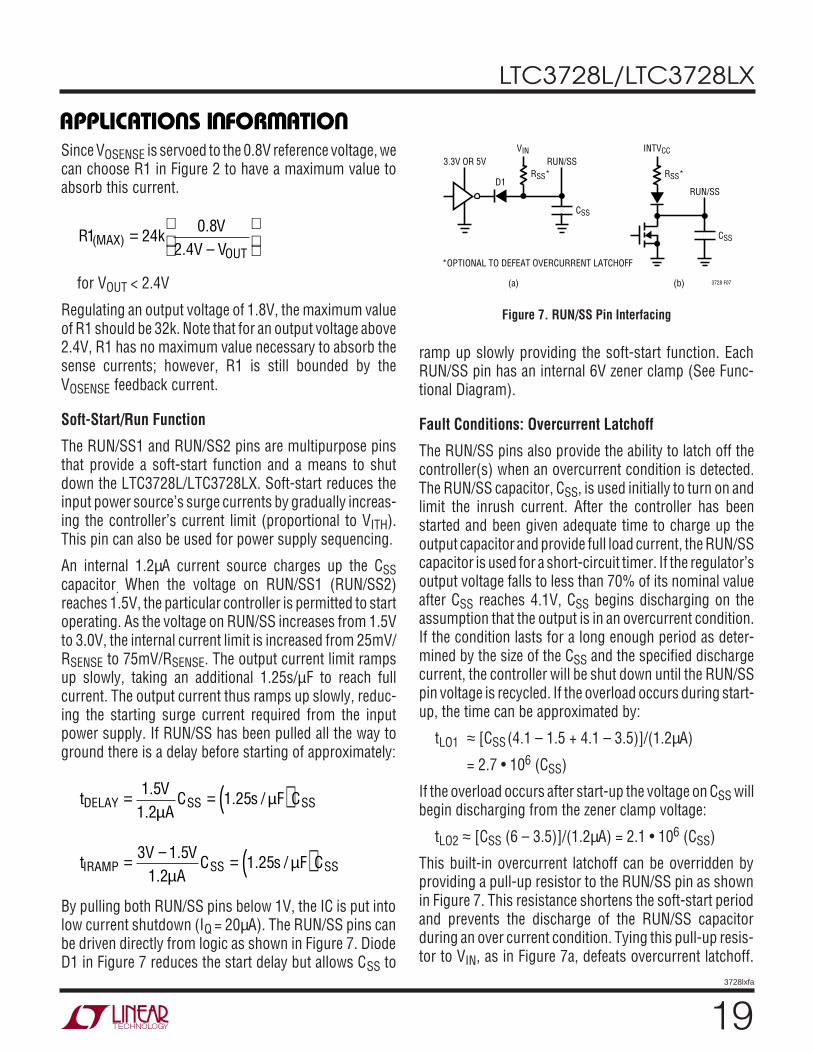
Soft-Start/Run Function
The RUN/SS1 and RUN/SS2 pins are multipurpose pinsthat provide a soft-start function and a means to shutdown the LTC3728L/LTC3728LX. Soft-start reduces theinput power source’s surge currents by gradually increas-ing the controller’s current limit (proportional to VITH).This pin can also be used for power supply sequencing.
An internal 1.2µA current source charges up the CSScapacitor. When the voltage on RUN/SS1 (RUN/SS2)reaches 1.5V, the particular controller is permitted to startoperating. As the voltage on RUN/SS increases from 1.5Vto 3.0V, the internal current limit is increased from 25mV/RSENSE to 75mV/RSENSE. The output current limit rampsup slowly, taking an additional 1.25s/µF to reach fullcurrent. The output current thus ramps up slowly, reduc-ing the starting surge current required from the inputpower supply. If RUN/SS has been pulled all the way toground there is a delay before starting of approximately:
tVA
C s F CDELAY SS SS=µ
= µ( )1 51 2
1 25.
.. /
tV V
AC s F CIRAMP SS SS= −
µ= µ( )3 1 5
1 21 25
..
. /
By pulling both RUN/SS pins below 1V, the IC is put intolow current shutdown (IQ = 20µA). The RUN/SS pins canbe driven directly from logic as shown in Figure 7. DiodeD1 in Figure 7 reduces the start delay but allows CSS to
ramp up slowly providing the soft-start function. EachRUN/SS pin has an internal 6V zener clamp (See Func-tional Diagram).
Fault Conditions: Overcurrent Latchoff
The RUN/SS pins also provide the ability to latch off thecontroller(s) when an overcurrent condition is detected.The RUN/SS capacitor, CSS, is used initially to turn on andlimit the inrush current. After the controller has beenstarted and been given adequate time to charge up theoutput capacitor and provide full load current, the RUN/SScapacitor is used for a short-circuit timer. If the regulator’soutput voltage falls to less than 70% of its nominal valueafter CSS reaches 4.1V, CSS begins discharging on theassumption that the output is in an overcurrent condition.If the condition lasts for a long enough period as deter-mined by the size of the CSS and the specified dischargecurrent, the controller will be shut down until the RUN/SSpin voltage is recycled. If the overload occurs during start-up, the time can be approximated by:
tLO1 ≈ [CSS(4.1 – 1.5 + 4.1 – 3.5)]/(1.2µA)
= 2.7 • 106 (CSS)
If the overload occurs after start-up the voltage on CSS willbegin discharging from the zener clamp voltage:
tLO2 ≈ [CSS (6 – 3.5)]/(1.2µA) = 2.1 • 106 (CSS)
This built-in overcurrent latchoff can be overridden byproviding a pull-up resistor to the RUN/SS pin as shownin Figure 7. This resistance shortens the soft-start periodand prevents the discharge of the RUN/SS capacitorduring an over current condition. Tying this pull-up resis-tor to VIN, as in Figure 7a, defeats overcurrent latchoff.
Figure 7. RUN/SS Pin Interfacing
3.3V OR 5V RUN/SSVIN INTVCC
RUN/SSD1
CSS
RSS*
CSS
RSS*
3728 F07(a) (b)
*OPTIONAL TO DEFEAT OVERCURRENT LATCHOFF
APPLICATIO S I FOR ATIO
WU UU
20
LTC3728L/LTC3728LX
3728lxfa
Diode-connecting this pull-up resistor to INTVCC, as inFigure 7b, eliminates any extra supply current duringcontroller shutdown while eliminating the INTVCC loadingfrom preventing controller start-up.
Why should you defeat overcurrent latchoff? During theprototyping stage of a design, there may be a problemwith noise pickup or poor layout causing the protectioncircuit to latch off. Defeating this feature will easily allowtroubleshooting of the circuit and PC layout. The internalshort-circuit and foldback current limiting still remainsactive, thereby protecting the power supply system fromfailure. After the design is complete, a decision can bemade whether to enable the latchoff feature.
The value of the soft-start capacitor CSS may need to bescaled with output voltage, output capacitance and loadcurrent characteristics. The minimum soft-start capaci-tance is given by:
CSS > (COUT )(VOUT) (10 –4) (RSENSE)
The minimum recommended soft-start capacitor ofCSS = 0.1µF will be sufficient for most applications.
Fault Conditions: Current Limit and Current Foldback
The current comparators have a maximum sense voltageof 75mV resulting in a maximum MOSFET current of75mV/RSENSE. The maximum value of current limit gener-ally occurs with the largest VIN at the highest ambienttemperature, conditions that cause the highest powerdissipation in the top MOSFET.
Each controller includes current foldback to help furtherlimit load current when the output is shorted to ground.The foldback circuit is active even when the overloadshutdown latch described above is overridden. If theoutput falls below 70% of its nominal output level, then themaximum sense voltage is progressively lowered from75mV to 25mV. Under short-circuit conditions with verylow duty cycles, the controller will begin cycle skipping inorder to limit the short-circuit current. In this situation thebottom MOSFET will be dissipating most of the power butless than in normal operation. The short-circuit ripplecurrent is determined by the minimum on-time tON(MIN) ofeach controller (typically 100ns), the input voltage andinductor value:
The overvoltage crowbar is designed to blow a systeminput fuse when the output voltage of the regulator risesmuch higher than nominal levels. The crowbar causeshuge currents to flow, that blow the fuse to protect againsta shorted top MOSFET if the short occurs while thecontroller is operating.
A comparator monitors the output for overvoltage condi-tions. The comparator (OV) detects overvoltage faultsgreater than 7.5% above the nominal output voltage.When this condition is sensed, the top MOSFET is turnedoff and the bottom MOSFET is turned on until the overvolt-age condition is cleared. The output of this comparator isonly latched by the overvoltage condition itself and willtherefore allow a switching regulator system having a poorPC layout to function while the design is being debugged.The bottom MOSFET remains on continuously for as longas the OV condition persists; if VOUT returns to a safe level,normal operation automatically resumes. A shorted topMOSFET will result in a high current condition which willopen the system fuse. The switching regulator will regu-late properly with a leaky top MOSFET by altering the dutycycle to accommodate the leakage.
Phase-Locked Loop and Frequency Synchronization
The IC has a phase-locked loop comprised of an internalvoltage controlled oscillator and phase detector. Thisallows the top MOSFET turn-on to be locked to the risingedge of an external source. The frequency range of thevoltage controlled oscillator is ±50% around the centerfrequency fO. A voltage applied to the PLLFLTR pin of 1.2Vcorresponds to a frequency of approximately 400kHz. Thenominal operating frequency range of the IC is 260kHz to550kHz.
APPLICATIO S I FOR ATIO
WU UU
21
LTC3728L/LTC3728LX
3728lxfa
The phase detector used is an edge sensitive digital typewhich provides zero degrees phase shift between theexternal and internal oscillators. This type of phase detec-tor will not lock up on input frequencies close to theharmonics of the VCO center frequency. The PLL hold-inrange, ∆fH, is equal to the capture range, ∆fC:
∆fH = ∆fC = ±0.5 fO (260kHz-550kHz)
The output of the phase detector is a complementary pairof current sources charging or discharging the externalfilter network on the PLLFLTR pin. A simplified blockdiagram is shown in Figure 7.
If the external frequency (fPLLIN) is greater than the oscil-lator frequency f0SC, current is sourced continuously,pulling up the PLLFLTR pin. When the external frequencyis less than f0SC, current is sunk continuously, pullingdown the PLLFLTR pin. If the external and internal fre-quencies are the same but exhibit a phase difference, thecurrent sources turn on for an amount of time correspond-ing to the phase difference. Thus the voltage on thePLLFLTR pin is adjusted until the phase and frequency ofthe external and internal oscillators are identical. At thisstable operating point the phase comparator output isopen and the filter capacitor CLP holds the voltage. The IC’sPLLIN pin must be driven from a low impedance sourcesuch as a logic gate located close to the pin. When usingmultiple ICs for a phase-locked system, the PLLFLTR pinof the master oscillator should be biased at a voltage thatwill guarantee the slave oscillator(s) ability to lock onto themaster’s frequency. A DC voltage of 0.7V to 1.7V appliedto the master oscillator’s PLLFLTR pin is recommended inorder to meet this requirement. The resultant operatingfrequency can range from 300kHz to 500kHz.
The loop filter components (CLP, RLP) smooth out thecurrent pulses from the phase detector and provide astable input to the voltage controlled oscillator. The filtercomponents CLP and RLP determine how fast the loopacquires lock. Typically RLP =10kΩ and CLP is 0.01µF to0.1µF.
Minimum On-Time Considerations
Minimum on-time tON(MIN) is the smallest time durationthat each controller is capable of turning on the topMOSFET. It is determined by internal timing delays and thegate charge required to turn on the top MOSFET. Low dutycycle applications may approach this minimum on-timelimit and care should be taken to ensure that
tVV f
ON MINOUT
IN( )
( )<
If the duty cycle falls below what can be accommodated bythe minimum on-time, the controller will begin to skipcycles. The output voltage will continue to be regulated,but the ripple voltage and current will increase.
The minimum on-time for each controller is approximately100ns. However, as the peak sense voltage decreases theminimum on-time gradually increases up to about 150ns.This is of particular concern in forced continuous applica-tions with low ripple current at light loads. If the duty cycledrops below the minimum on-time limit in this situation,a significant amount of cycle skipping can occur withcorrespondingly larger current and voltage ripple.
FCB Pin Operation
The FCB pin can be used to regulate a secondary windingor as a logic level input. Continuous operation is forced onboth controllers when the FCB pin drops below 0.8V.During continuous mode, current flows continuously inthe transformer primary. The secondary winding(s) drawcurrent only when the bottom, synchronous switch is on.When primary load currents are low and/or the VIN/VOUTratio is low, the synchronous switch may not be on for asufficient amount of time to transfer power from theoutput capacitor to the secondary load. Forced continuousoperation will support secondary windings providing thereis sufficient synchronous switch duty factor. Thus, theFCB input pin removes the requirement that power mustbe drawn from the inductor primary in order to extract
APPLICATIO S I FOR ATIO
WU UU
22
LTC3728L/LTC3728LX
3728lxfa
loop is reduced depending upon the maximum load stepspecifications. Voltage positioning can easily be added toeither or both controllers by loading the ITH pin with aresistive divider having a Thevenin equivalent voltagesource equal to the midpoint operating voltage range ofthe error amplifier, or 1.2V (see Figure 8).
The resistive load reduces the DC loop gain while main-taining the linear control range of the error amplifier. Themaximum output voltage deviation can theoretically bereduced to half or alternatively the amount of outputcapacitance can be reduced for a particular application. Acomplete explanation is included in Design Solutions 10.(See www.linear-tech.com)
power from the auxiliary windings. With the loop incontinuous mode, the auxiliary outputs may nominally beloaded without regard to the primary output load.
The secondary output voltage VSEC is normally set asshown in Figure 6a by the turns ratio N of the transformer:
VSEC ≅ (N + 1) VOUT
However, if the controller goes into Burst Mode operationand halts switching due to a light primary load current,then VSEC will droop. An external resistive divider fromVSEC to the FCB pin sets a minimum voltage VSEC(MIN):
V VRR
SEC MIN( ) .≈ +
0 8 1
65
where R5 and R6 are shown in Figure 2.
If VSEC drops below this level, the FCB voltage forcestemporary continuous switching operation until VSEC isagain above its minimum.
In order to prevent erratic operation if no external connec-tions are made to the FCB pin, the FCB pin has a 0.18µAinternal current source pulling the pin high. Include thiscurrent when choosing resistor values R5 and R6.
The following table summarizes the possible states avail-able on the FCB pin:Table 1FCB Pin Condition
0V to 0.75V Forced Continuous Both Controllers(Current Reversal Allowed—Burst Inhibited)
0.85V < VFCB < 4.3V Minimum Peak Current InducesBurst Mode OperationNo Current Reversal Allowed
Feedback Resistors Regulating a Secondary Winding
>4.8V Burst Mode Operation DisabledConstant Frequency Mode EnabledNo Current Reversal AllowedNo Minimum Peak Current
Voltage Positioning
Voltage positioning can be used to minimize peak-to-peakoutput voltage excursions under worst-case transientloading conditions. The open-loop DC gain of the control
APPLICATIO S I FOR ATIO
WU UU
ITH
RCRT1
INTVCC
CC
3728 F08
LTC3728L/LTC3728LX
RT2
Figure 8. Active Voltage PositioningApplied to the LTC3728L/LTC3728LX
Efficiency Considerations
The percent efficiency of a switching regulator is equal tothe output power divided by the input power times 100%.It is often useful to analyze individual losses to determinewhat is limiting the efficiency and which change wouldproduce the most improvement. Percent efficiency can beexpressed as:
%Efficiency = 100% – (L1 + L2 + L3 + ...)
where L1, L2, etc. are the individual losses as a percentageof input power.
Although all dissipative elements in the circuit producelosses, four main sources usually account for most of thelosses in LTC3728L/LTC3728LX circuits: 1) IC VIN current(including loading on the 3.3V internal regulator), 2)INTVCC regulator current, 3) I2R losses, 4) Topside MOSFETtransition losses.
1. The VIN current has two components: the first is the DCsupply current given in the Electrical Characteristics table,
23
LTC3728L/LTC3728LX
3728lxfa
4. Transition losses apply only to the topside MOSFET(s),and become significant only when operating at high inputvoltages (typically 15V or greater). Transition losses canbe estimated from:
Transition Loss = VIN( )
( )
( )( ) +
2
2
15
1
• •
–
IR
C fV V V
MAXDR
MILLERTH TH
Other “hidden” losses such as copper trace and internalbattery resistances can account for an additional 5% to 10%efficiency degradation in portable systems. It is very impor-tant to include these “system” level losses during the de-sign phase. The internal battery and fuse resistance lossescan be minimized by making sure that CIN has adequatecharge storage and very low ESR at the switching frequency.A 25W supply will typically require a minimum of 20µF to40µF of capacitance having a maximum of 20mΩ to 50mΩof ESR. The LTC3728L 2-phase architecture typically halvesthis input capacitance requirement over competing solu-tions. Other losses including Schottky conduction lossesduring dead-time and inductor core losses generally ac-count for less than 2% total additional loss.
Checking Transient Response
The regulator loop response can be checked by looking atthe load current transient response. Switching regulatorstake several cycles to respond to a step in DC (resistive)load current. When a load step occurs, VOUT shifts by anamount equal to ∆ILOAD (ESR), where ESR is the effectiveseries resistance of COUT. ∆ILOAD also begins to charge ordischarge COUT generating the feedback error signal thatforces the regulator to adapt to the current change andreturn VOUT to its steady-state value. During this recoverytime VOUT can be monitored for excessive overshoot orringing, which would indicate a stability problem. OPTI-LOOP compensation allows the transient response to beoptimized over a wide range of output capacitance andESR values. The availability of the ITH pin not only allowsoptimization of control loop behavior but also provides aDC coupled and AC filtered closed loop response testpoint. The DC step, rise time and settling at this test point
which excludes MOSFET driver and control currents; thesecond is the current drawn from the 3.3V linear regulatoroutput. VIN current typically results in a small (<0.1%) loss.
2. INTVCC current is the sum of the MOSFET driver andcontrol currents. The MOSFET driver current results fromswitching the gate capacitance of the power MOSFETs.Each time a MOSFET gate is switched from low to high tolow again, a packet of charge dQ moves from INTVCC toground. The resulting dQ/dt is a current out of INTVCC thatis typically much larger than the control circuit current. Incontinuous mode, IGATECHG =f(QT+QB), where QT and QBare the gate charges of the topside and bottom sideMOSFETs.
Supplying INTVCC power through the EXTVCC switch inputfrom an output-derived source will scale the VIN currentrequired for the driver and control circuits by a factor of(Duty Cycle)/(Efficiency). For example, in a 20V to 5Vapplication, 10mA of INTVCC current results in approxi-mately 2.5mA of VIN current. This reduces the mid-currentloss from 10% or more (if the driver was powered directlyfrom VIN) to only a few percent.
3. I2R losses are predicted from the DC resistances of thefuse (if used), MOSFET, inductor, current sense resistor,and input and output capacitor ESR. In continuous modethe average output current flows through L and RSENSE,but is “chopped” between the topside MOSFET and thesynchronous MOSFET. If the two MOSFETs have approxi-mately the same RDS(ON), then the resistance of oneMOSFET can simply be summed with the resistances of L,RSENSE and ESR to obtain I2R losses. For example, if eachRDS(ON) = 30mΩ, RL = 50mΩ, RSENSE = 10mΩ and RESR= 40mΩ (sum of both input and output capacitancelosses), then the total resistance is 130mΩ. This results inlosses ranging from 3% to 13% as the output currentincreases from 1A to 5A for a 5V output, or a 4% to 20%loss for a 3.3V output. Efficiency varies as the inversesquare of VOUT for the same external components andoutput power level. The combined effects of increasinglylower output voltages and higher currents required byhigh performance digital systems is not doubling butquadrupling the importance of loss terms in the switchingregulator system!
APPLICATIO S I FOR ATIO
WU UU
24
LTC3728L/LTC3728LX
3728lxfa
truly reflects the closed loop response. Assuming a pre-dominantly second order system, phase margin and/ordamping factor can be estimated using the percentage ofovershoot seen at this pin. The bandwidth can also beestimated by examining the rise time at the pin. The ITHexternal components shown in the Figure 1 circuit willprovide an adequate starting point for most applications.
The ITH series RC-CC filter sets the dominant pole-zeroloop compensation. The values can be modified slightly(from 0.5 to 2 times their suggested values) to optimizetransient response once the final PC layout is done and theparticular output capacitor type and value have beendetermined. The output capacitors need to be selectedbecause the various types and values determine the loopgain and phase. An output current pulse of 20% to 80% offull-load current having a rise time of 1µs to 10µs willproduce output voltage and ITH pin waveforms that willgive a sense of the overall loop stability without breakingthe feedback loop. Placing a power MOSFET directlyacross the output capacitor and driving the gate with anappropriate signal generator is a practical way to producea realistic load step condition. The initial output voltagestep resulting from the step change in output current maynot be within the bandwidth of the feedback loop, so thissignal cannot be used to determine phase margin. This iswhy it is better to look at the ITH pin signal which is in thefeedback loop and is the filtered and compensated controlloop response. The gain of the loop will be increased byincreasing RC and the bandwidth of the loop will beincreased by decreasing CC. If RC is increased by the samefactor that CC is decreased, the zero frequency will be keptthe same, thereby keeping the phase shift the same in themost critical frequency range of the feedback loop. Theoutput voltage settling behavior is related to the stability ofthe closed-loop system and will demonstrate the actualoverall supply performance.
A second, more severe transient is caused by switching inloads with large (>1µF) supply bypass capacitors. Thedischarged bypass capacitors are effectively put in parallelwith COUT, causing a rapid drop in VOUT. No regulator canalter its delivery of current quickly enough to prevent thissudden step change in output voltage if the load switchresistance is low and it is driven quickly. If the ratio ofCLOAD to COUT is greater than1:50, the switch rise time
should be controlled so that the load rise time is limited toapproximately 25 • CLOAD. Thus a 10µF capacitor wouldrequire a 250µs rise time, limiting the charging current toabout 200mA.
Automotive Considerations: Plugging into theCigarette Lighter
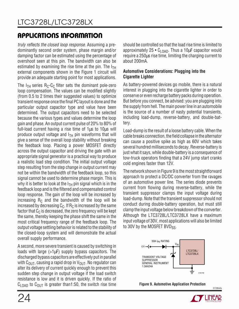
As battery-powered devices go mobile, there is a naturalinterest in plugging into the cigarette lighter in order toconserve or even recharge battery packs during operation.But before you connect, be advised: you are plugging intothe supply from hell. The main power line in an automobileis the source of a number of nasty potential transients,including load-dump, reverse-battery, and double-bat-tery.
Load-dump is the result of a loose battery cable. When thecable breaks connection, the field collapse in the alternatorcan cause a positive spike as high as 60V which takesseveral hundred milliseconds to decay. Reverse-battery isjust what it says, while double-battery is a consequence oftow-truck operators finding that a 24V jump start crankscold engines faster than 12V.
The network shown in Figure 9 is the most straightforwardapproach to protect a DC/DC converter from the ravagesof an automotive power line. The series diode preventscurrent from flowing during reverse-battery, while thetransient suppressor clamps the input voltage duringload-dump. Note that the transient suppressor should notconduct during double-battery operation, but must stillclamp the input voltage below breakdown of the converter.Although the LTC3728L/LTC3728LX have a maximuminput voltage of 30V, most applications will also be limitedto 30V by the MOSFET BVDSS.
As a design example for one channel, assume VIN =12V(nominal), VIN = 22V(max), VOUT = 1.8V, IMAX = 5A,and f = 300kHz.
The inductance value is chosen first based on a 30% ripplecurrent assumption. The highest value of ripple currentoccurs at the maximum input voltage. Tie the PLLFLTR pinto a resistive divider from the INTVCC pin, generating 0.7Vfor 300kHz operation. The minimum inductance for 30%ripple current is:
∆IVf L
VV
LOUT OUT
IN=
( )( )–1
A 4.7µH inductor will produce 23% ripple current and a3.3µH will result in 33%. The peak inductor current will bethe maximum DC value plus one half the ripple current, or5.84A, for the 3.3µH value. Increasing the ripple currentwill also help ensure that the minimum on-time of 100nsis not violated. The minimum on-time occurs at maximumVIN:
tV
V fV
V kHznsON MIN
OUT
IN MAX( )
( )
.( )
= = =1 822 300
273
The RSENSE resistor value can be calculated by using themaximum current sense voltage specification with someaccommodation for tolerances:
RmV
ASENSE ≤ ≈ Ω60
5 840 01
..
Since the output voltage is below 2.4V the output resistivedivider will need to be sized to not only set the outputvoltage but also to absorb the SENSE pin’s specified inputcurrent.
R kV
V V
kV
V Vk
MAXOUT
1 240 8
2 4
240 8
2 4 1 832
( ).
. –
.. – .
=
=
=
Choosing 1% resistors: R1 = 25.5k and R2 = 32.4k yieldsan output voltage of 1.816V.
The power dissipation on the top side MOSFET can beeasily estimated. Choosing a Fairchild FDS6982S dualMOSFET results in: RDS(ON) = 0.035Ω/0.022Ω, CMILLER =215pF. At maximum input voltage with T(estimated) =50°C:
PVV
C C
VA
pF
kHz mW
MAIN = ( ) + ° °[ ]Ω( ) + ( )
Ω( )( )
+
( ) =
1 822
5 1 0 005 50 25
0 035 2252
4 215
15 2 3
12 3
300 332
2
2
.( . )( – ) •
. •
– . .
A short-circuit to ground will result in a folded back currentof:
ImV ns V
HASC =
Ω µ
=25
0 0112
120 223 3
2 1.
–( )
..
with a typical value of RDS(ON) and δ = (0.005/°C)(20) = 0.1.The resulting power dissipated in the bottom MOSFET is:
PV V
VA
mW
SYNC = ( ) ( ) Ω( )=
22 1 822
2 1 1 125 0 022
100
2– .. . .
which is less than under full-load conditions.
CIN is chosen for an RMS current rating of at least 3A attemperature assuming only this channel is on. COUT ischosen with an ESR of 0.02Ω for low output ripple. Theoutput ripple in continuous mode will be highest at themaximum input voltage. The output voltage ripple due toESR is approximately:
VORIPPLE = RESR (∆IL) = 0.02Ω(1.67A) = 33mVP–P
APPLICATIO S I FOR ATIO
WU UU
26
LTC3728L/LTC3728LX
3728lxfa
PC Board Layout Checklist
When laying out the printed circuit board, the followingchecklist should be used to ensure proper operation of theIC. These items are also illustrated graphically in thelayout diagram of Figure 10. The Figure 11 illustrates thecurrent waveforms present in the various branches of the2-phase synchronous regulators operating in the continu-ous mode. Check the following in your layout:
1. Are the top N-channel MOSFETs M1 and M3 locatedwithin 1cm of each other with a common drain connectionat CIN? Do not attempt to split the input decoupling for thetwo channels as it can cause a large resonant loop.
2. Are the signal and power grounds kept separate? Thecombined IC signal ground pin and the ground return ofCINTVCC must return to the combined COUT (–) terminals.The path formed by the top N-channel MOSFET, Schottkydiode and the CIN capacitor should have short leads andPC trace lengths. The output capacitor (–) terminalsshould be connected as close as possible to the (–)terminals of the input capacitor by placing the capacitorsnext to each other and away from the Schottky loopdescribed above.
3. Do the LTC3728L/LTC3728LX VOSENSE pins’ resistivedividers connect to the (+) terminals of COUT? The resistivedivider must be connected between the (+) terminal of
COUT and signal ground. The R2 and R4 connectionsshould not be along the high current input feeds from theinput capacitor(s).
4. Are the SENSE – and SENSE + leads routed togetherwith minimum PC trace spacing? The filter capacitorbetween SENSE + and SENSE – should be as close aspossible to the IC. Ensure accurate current sensing withKelvin connections at the SENSE resistor.
5. Is the INTVCC decoupling capacitor connected close tothe IC, between the INTVCC and the power ground pins?This capacitor carries the MOSFET drivers current peaks.
An additional 1µF ceramic capacitor placed immediatelynext to the INTVCC and PGND pins can help improve noiseperformance substantially.
6. Keep the switching nodes (SW1, SW2), top gate nodes(TG1, TG2), and boost nodes (BOOST1, BOOST2) awayfrom sensitive small-signal nodes, especially from theopposites channel’s voltage and current sensing feedbackpins. All of these nodes have very large and fast movingsignals and therefore should be kept on the “output side”of the LTC3728L/LTC3728LX and occupy minimum PCtrace area.
APPLICATIO S I FOR ATIO
WU UU
Figure 11. Branch Current Waveforms
RL1D1
L1SW1 RSENSE1 VOUT1
COUT1+
VIN
CERAMIC
CIN
RIN +
RL2D2BOLD LINES INDICATEHIGH SWITCHING CURRENT. KEEP LINESTO A MINIMUM LENGTH.
L2SW2
3728 F11
RSENSE2 VOUT2
COUT2+
CERAMIC
28
LTC3728L/LTC3728LX
3728lxfa
APPLICATIO S I FOR ATIO
WU UU
7. Use a modified “star ground” technique: a low imped-ance, large copper area central grounding point on thesame side of the PC board as the input and outputcapacitors with tie-ins for the bottom of the INTVCCdecoupling capacitor, the bottom of the voltage feedbackresistive divider and the SGND pin of the IC.
PC Board Layout Debugging
Start with one controller on at a time. It is helpful to use aDC-50MHz current probe to monitor the current in theinductor while testing the circuit. Monitor the outputswitching node (SW pin) to synchronize the oscilloscopeto the internal oscillator and probe the actual outputvoltage as well. Check for proper performance over theoperating voltage and current range expected in the appli-cation. The frequency of operation should be maintainedover the input voltage range down to dropout and until theoutput load drops below the low current operation thresh-old—typically 10% to 20% of the maximum designedcurrent level in Burst Mode operation.
The duty cycle percentage should be maintained fromcycle to cycle in a well-designed, low noise PCB imple-mentation. Variation in the duty cycle at a subharmonicrate can suggest noise pickup at the current or voltagesensing inputs or inadequate loop compensation. Over-compensation of the loop can be used to tame a poor PClayout if regulator bandwidth optimization is not required.Only after each controller is checked for its individualperformance should both controllers be turned on at thesame time. A particularly difficult region of operation iswhen one controller channel is nearing its current com-parator trip point when the other channel is turning on itstop MOSFET. This occurs around 50% duty cycle on eitherchannel due to the phasing of the internal clocks and maycause minor duty cycle jitter.
Short-circuit testing can be performed to verify properovercurrent latchoff, or 5µA can be provided to the RUN/SS pin(s) by resistors from VIN to prevent the short-circuitlatchoff from occurring.
Reduce VIN from its nominal level to verify operation of theregulator in dropout. Check the operation of the under-voltage lockout circuit by further lowering VIN while moni-toring the outputs to verify operation.
Investigate whether any problems exist only at higheroutput currents or only at higher input voltages. If prob-lems coincide with high input voltages and low outputcurrents, look for capacitive coupling between the BOOST,SW, TG, and possibly BG connections and the sensitivevoltage and current pins. The capacitor placed across thecurrent sensing pins needs to be placed immediatelyadjacent to the pins of the IC. This capacitor helps tominimize the effects of differential noise injection due tohigh frequency capacitive coupling. If problems are en-countered with high current output loading at lower inputvoltages, look for inductive coupling between CIN, Schottkyand the top MOSFET components to the sensitive currentand voltage sensing traces. In addition, investigate com-mon ground path voltage pickup between these compo-nents and the SGND pin of the IC.
An embarrassing problem, which can be missed in anotherwise properly working switching regulator, resultswhen the current sensing leads are hooked up backwards.The output voltage under this improper hookup will still bemaintained but the advantages of current mode controlwill not be realized. Compensation of the voltage loop willbe much more sensitive to component selection. Thisbehavior can be investigated by temporarily shorting outthe current sensing resistor—don’t worry, the regulatorwill still maintain control of the output voltage.
VIN: 7V TO 28VVOUT: 5V, 3A/3.3V, 6A/12V, 150mASWITCHING FREQUENCY = 250kHzMI, M2: FDS6982S OR VISHAY Si4810DYL1: SUMIDA CEP123-6R3MCT1: 10µH 1:1.8 — DALE LPE6562-A262 GAPPED E-CORE OR BH ELECTRONICS #501-0657 GAPPED TOROID
LT1121
+
+
220k
100k
1M
PGOOD
100k VPULL-UP(<7V)
59k
180pF
180pF
M1
M2
TYPICAL APPLICATIO S
U
30
LTC3728L/LTC3728LX
3728lxfa
TYPICAL APPLICATIO S
U
Figure 13. LTC3728L/LTC3728LX 5V/4A, 3.3V/5A Regulator with External Frequency Synchronization
0.1µF
4.7µF, 10V
+
22µF50V
M1PIN 4
PIN 4
Q1 Q2
Q3 Q4
M2
1µF
0.1µF
10Ω
0.008Ω
0.008Ω
1µF 50V
fSYNC
3.3V
0.1µF
10k
105k1%
100pF
8.06k
100pF
4.75k1000pF
1500pF
0.01µF1000pF
1000pF
1000pF
0.1µF
20k1%
63.4k1%
20k1%
RUN/SS1
SENSE1+
SENSE1–
VOSENSE1
PLLFLTR
PLLIN
FCB
ITH1
SGND
3.3VOUT
ITH2
VOSENSE2
SENSE2–
SENSE2+
PGOOD
TG1
SW1
BOOST1
VIN
BG1
EXTVCC
INTVCC
PGND
BG2
BOOST2
SW2
TG2
RUN/SS2
LTC3728L/LTC3728LX
L14.3µH
L24.3µH
150µF, 6.3V
180µF, 4V
GND
VOUT23.3V/5A
VOUT15V/4A
VIN7V TO28V
3728 F13
++
VIN: 7V TO 28VVOUT: 5V, 4A/3.3V, 5A
SWITCHING FREQUENCY = 250kHz TO 550kHzM1, M2: FDS6982S OR VISHAY Si4810DY
L1, L2: SUMIDA CDEP105-4R3MC-88OUTPUT CAPACITORS: PANASONIC SP SERIES
180pF
180pF
0.1µF
CMDSH-3TR
CMDSH-3TR
PGOOD
VPULL-UP(<7V)
1µF 50V
31
LTC3728L/LTC3728LX
3728lxfa
U
PACKAGE DESCRIPTIO
UH Package32-Lead Plastic QFN (5mm × 5mm)
(Reference LTC DWG # 05-08-1693)
(For purposes of clarity, drawings are not to scale)
5.00 ± 0.10(4 SIDES)
NOTE:1. DRAWING PROPOSED TO BE A JEDEC PACKAGE OUTLINE M0-220 VARIATION WHHD-(X) (TO BE APPROVED)2. DRAWING NOT TO SCALE3. ALL DIMENSIONS ARE IN MILLIMETERS4. DIMENSIONS OF EXPOSED PAD ON BOTTOM OF PACKAGE DO NOT INCLUDE MOLD FLASH. MOLD FLASH, IF PRESENT, SHALL NOT EXCEED 0.20mm ON ANY SIDE5. EXPOSED PAD SHALL BE SOLDER PLATED
PIN 1TOP MARK
0.40 ± 0.10
31
1
2
32
BOTTOM VIEW—EXPOSED PAD
3.45 ± 0.10(4-SIDES)
0.75 ± 0.05 R = 0.115TYP
0.23 ± 0.05(UH) QFN 0102
0.50 BSC
0.200 REF
0.00 – 0.050.57 ±0.05
3.45 ±0.05(4 SIDES)
4.20 ±0.05
5.35 ±0.05
0.23 ± 0.05 PACKAGE OUTLINE
0.50 BSC
RECOMMENDED SOLDER PAD LAYOUT
Information furnished by Linear Technology Corporation is believed to be accurate and reliable.However, no responsibility is assumed for its use. Linear Technology Corporation makes no represen-tation that the interconnection of its circuits as described herein will not infringe on existing patent rights.
GN Package28-Lead Plastic SSOP (Narrow .150 Inch)
(Reference LTC DWG # 05-08-1641)
.386 – .393*(9.804 – 9.982)
GN28 (SSOP) 0502
1 2 3 4 5 6 7 8 9 10 11 12
.229 – .244(5.817 – 6.198)
.150 – .157**(3.810 – 3.988)
202122232425262728 19 18 17
13 14
1615
.016 – .050(0.406 – 1.270)
.015 ± .004(0.38 ± 0.10)
× 45°
0° – 8° TYP.0075 – .0098(0.191 – 0.249)
.053 – .069(1.351 – 1.748)
.008 – .012(0.203 – 0.305)
.004 – .009(0.102 – 0.249)
.0250(0.635)
BSC
.033(0.838)
REF
.254 MIN
RECOMMENDED SOLDER PAD LAYOUT
.150 – .165
.0250 TYP.0165 ± .0015
.045 ±.005
*DIMENSION DOES NOT INCLUDE MOLD FLASH. MOLD FLASH SHALL NOT EXCEED 0.006" (0.152mm) PER SIDE**DIMENSION DOES NOT INCLUDE INTERLEAD FLASH. INTERLEAD FLASH SHALL NOT EXCEED 0.010" (0.254mm) PER SIDE
INCHES(MILLIMETERS)
NOTE:1. CONTROLLING DIMENSION: INCHES
2. DIMENSIONS ARE IN
3. DRAWING NOT TO SCALE
32
LTC3728L/LTC3728LX
3728lxfa
PART NUMBER DESCRIPTION COMMENTSLTC1628/LTC1628-PG/ 2-Phase, Dual Output Synchronous Step-Down Reduces CIN and COUT, Power Good Output Signal, Synchronizable,LTC1628-SYNC DC/DC Controller 3.5V ≤ VIN ≤ 36V, IOUT up to 20A, 0.8V ≤ VOUT ≤ 5VLTC1629/ 20A to 200A PolyPhaseTM Synchronous Controllers Expandable from 2-Phase to 12-Phase, Uses AllLTC1629-PG Surface Mount Components, No Heat Sink, VIN up to 36VLTC1702A No RSENSE 2-Phase Dual Synchronous Step-Down 550kHz, No Sense Resistor
ControllerLTC1708-PG 2-Phase, Dual Synchronous Controller with Mobile VID 3.5V ≤ VIN ≤ 36V, VID Sets VOUT1, PGOODLT1709/ High Efficiency, 2-Phase Synchronous Step-Down 1.3V ≤ VOUT ≤ 3.5V, Current Mode EnsuresLT1709-8 Switching Regulators with 5-Bit VID Accurate Current Sharing, 3.5V ≤ VIN ≤ 36VLTC1735 High Efficiency Synchronous Step-Down Output Fault Protection, 16-Pin SSOP
Switching RegulatorLTC1736 High Efficiency Synchronous Controller with 5-Bit Mobile Output Fault Protection, 24-Pin SSOP,
VID Control 3.5V ≤ VIN ≤ 36VLTC1778/LTC1778-1 No RSENSE Current Mode Synchronous Step-Down Up to 97% Efficiency, 4V ≤ VIN ≤ 36V, 0.8V ≤ VOUT ≤ (0.9)(VIN),
Controllers IOUT up to 20ALTC1929/ 2-Phase Synchronous Controllers Up to 42A, Uses All Surface Mount Components,LTC1929-PG No Heat Sinks, 3.5V ≤ VIN ≤ 36VLTC3708 Dual, 2-Phase, DC/DC Controller with Output Tracking Current Mode, No RSENSE, Up/Down Tracking, SynchronizableLTC3711 No RSENSE Current Mode Synchronous Step-Down Up to 97% Efficiency, Ideal for Pentium® III Processors,
Controller with Digital 5-Bit Interface 0.925V ≤ VOUT ≤ 2V, 4V ≤ VIN ≤ 36V, IOUT up to 20ALTC3728 Dual, 550kHz, 2-Phase Synchronous Step-Down Dual 180° Phased Controllers, VIN 3.5V to 35V, 99% Duty Cycle,
Controller 5x5QFN, SSOP-28LTC3729 20A to 200A, 550kHz PolyPhase Synchronous Controller Expandable from 2-Phase to 12-Phase, Uses all Surface Mount
Components, VIN up to 36VLTC3731 3- to 12-Phase Step-Down Synchronous Controller 60A to 240A Output Current, 0.6V ≤ VOUT ≤ 6V, 4.5V ≤ VIN ≤ 32VNo RSENSE and PolyPhase are trademarks of Linear Technology Corporation. Pentium is a registered trademark of Intel Corporation.
RELATED PARTS
U
TYPICAL APPLICATIO
Figure 14. Multioutput PolyPhase Application
PHASMD
CLKOUT
TG1
TG2
0°
I1
I3
I2
I4
90°
OPEN180°
U1LTC3729
BUCK: 2.5V/15A
BUCK: 2.5V/15A
PLLIN
TG1
TG2
90°
90°
270°U2
LTC3728L/LTC3728LX
BUCK: 1.5V/15A
2.5VO/30A
CIN
IIN12VIN
*INPUT RIPPLE CURRENT CANCELLATION INCREASES THE RIPPLE FREQUENCY AND REDUCES THE RMS INPUT RIPPLE CURRENT THUS, SAVING INPUT CAPACITORS
IIN*
1.5VO/15A
1.8VO/15A
3728 F14
BUCK: 1.8V/15A
I1
I2
I3
I4
Linear Technology Corporation1630 McCarthy Blvd., Milpitas, CA 95035-7417(408) 432-1900 FAX: (408) 434-0507 www.linear.com LINEAR TECHNOLOGY CORPORATION 2002