392 JOURNAL OF MICROELECTROMECHANICAL SYSTEMS, VOL. 14, NO. 2, APRIL 2005
Stamp-and-Stick Room-Temperature BondingTechnique for Microdevices
Srinath Satyanarayana, Rohit N. Karnik, and Arunava Majumdar, Fellow, ASME
Abstract—Multilayer MEMS and microfluidic designs usingdiverse materials demand separate fabrication of device compo-nents followed by assembly to make the final device. Structuraland moving components, labile bio-molecules, fluids and temper-ature-sensitive materials place special restrictions on the bondingprocesses that can be used for assembly of MEMS devices. Wedescribe a room temperature “stamp and stick (SAS)” transferbonding technique for silicon, glass and nitride surfaces usinga UV curable adhesive. Alternatively, poly(dimethylsiloxane)(PDMS) can also be used as the adhesive; this is particularlyuseful for bonding PDMS devices. A thin layer of adhesive isfirst spun on a flat wafer. This adhesive layer is then selectivelytransferred to the device chip from the wafer using a stampingprocess. The device chip can then be aligned and bonded to otherchips/wafers. This bonding process is conformal and works evenon surfaces with uneven topography. This aspect is especiallyrelevant to microfluidics, where good sealing can be difficult toobtain with channels on uneven surfaces. Burst pressure testssuggest that wafer bonds using the UV curable adhesive couldwithstand pressures of 700 kPa (7 atmospheres); those with PDMScould withstand 200 to 700 kPa (2–7 atmospheres) depending onthe geometry and configuration of the device. [1267]
Index Terms—Poly(dimethylsiloxane) (PDMS), room temper-ature, microelectromechanical systems (MEMS), microfluidics,transfer bonding, ultraviolet (UV) curable adhesive.
I. INTRODUCTION
WAFER and chip bonding techniques are critical steps infabrication and assembly of MEMS devices. Bonding
techniques can be briefly classified into two major cate-gories—direct bonding and bonding with an intermediate layer.
A. Direct Bonding
Anodic bonding, fusion bonding, and activated surfacebonding [1], [2] fall in this category. For anodic bonding,the wafers are cleaned extensively, aligned, and brought intopressure contact. High voltage ( kV) and high temperature( C) cause an irreversible bond to form between thesubstrates. Anodic bonding works well for bonding glass orglass coated substrates with silicon and nitride substrates.
Manuscript received February 10, 2004; revised July 17, 2004. This work wassupported by the SIMBIOSYS program of DARPA, the Innovative MolecularAnalysis Techniques (IMAT) program of the National Cancer Institute (NIH),the Department of Energy and the NSF. Subject Editor G. B. Hocker.
S. Satyanarayana and R. N. Karnik are with the Department of MechanicalEngineering, University of California, Berkeley, CA 94720-1740 USA.
A. Majumdar is with the Department of Mechanical Engineering, Universityof California, Berkeley, CA 94720-1740 USA and also with the Materials Sci-ences Division, Lawrence Berkeley National Laboratory, Berkeley, CA 94720USA (e-mail: [email protected]).
Digital Object Identifier 10.1109/JMEMS.2004.839334
Fusion bonding relies on the attractive forces that exist be-tween extremely clean flat surfaces in contact to form a strongbond between them. This bonding process requires extensiveprecleaning procedures and the alignment and bonding processis usually performed under vacuum with external pressuresto help form good contact. The bonding process is followedby a thermal cycling process to strengthen the bond. Fusionbonding works very well for bonding silicon wafers. In the caseof surface activation bonding, the substrates are pre-treatedwith oxygen plasma, hydration processes or other chemicalsto increase the reactivity, and then brought into contact withor without external pressure and high temperature to form anirreversible bond. The effect of surface treatment processeslasts only for a small time interval and the bonding processesincluding alignment need to be completed within this timewindow. Activation with oxygen plasma [3] has been usedextensively for bonding PDMS devices to PDMS or glass,which are commonly used materials in prototyping microflu-idic devices. Liu et al. [4] have bonded PDMS to PDMS andglass by incubating the device with the two surfaces to bebonded in contact at 80 C. Lin et al. [5], [6], and Cheng et al.[7] have demonstrated localized fusion bonding process eitherusing patterned micro heaters or using a focused laser. Local-ized heating eliminates the thermal cycling of the entire waferduring the bonding process. However, this bonding techniquerequires additional lithography steps.
B. Bonding With Intermediate Layer
Adhesive bonding, eutectic bonding, solder bonding, andthermocompression bonding fall in this category. Adhesivebonding [1], [2] does not require high temperatures or voltages,but requires a thin adhesive layer on the device, which isusually obtained by spin coating. However, spin coating is a bigproblem when the wafers to be bonded have nonuniform topog-raphy. Some typical adhesives used are epoxy, spin-on-glassand UV curable glue. Eutectic bonding [8] uses a thin goldlayer as an adhesive to bond silicon wafers. The wafers to bebonded are brought into contact and the temperature is raisedto gold-silicon eutectic point to form an irreversible bond. Linand others [5]–[7] improved this process to bond locally usingpatterned gold lines and in situ electrical heating. Localizedbonding overcomes the high temperature problem but requiresthe deposition and patterning of one or more additional bondinglayers (gold, silicon). This may not be compatible with somedevice materials like plastics and polymers or with somefabrication processes. Solder bonding and thermocompressionbonding again involve the deposition and patterning of addi-tional layers like solder or other soft metals and use either heat
SATYANARAYANA et al.: STAMP-AND-STICK ROOM-TEMPERATURE BONDING TECHNIQUE FOR MICRODEVICES 393
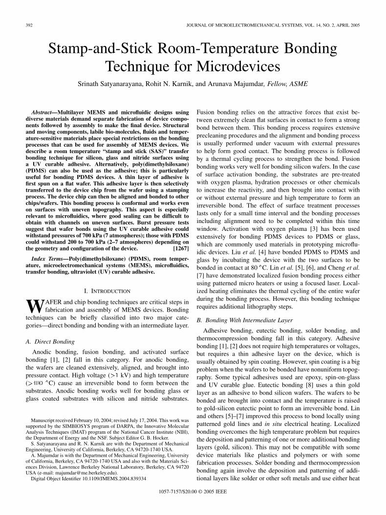
Fig. 1. Adhesive transfer process. (a) Uniform adhesive layer on a waferobtained by spinning, (b) the cover wafer with patterns brought into contactwith the adhesive, (c) selective transfer of the adhesive to the cover wafer,and (d) the cover wafer aligned with a device wafer, brought into contact andbonded.
and/or pressure to form bonds between substrates. Detailedanalysis of these bonding processes and additional referencescan be found in the review paper by Schmidt [1]. Recently,Noh et al. [9] have demonstrated a conformal bonding processwhere intermediate parylene layers, deposited on the wafers tobe bonded, were selectively heated using variable frequencymicrowave to form a bond. Parylene deposition is conformaland it is also a biocompatible polymer, but additional lithog-raphy steps are required to limit the bonding to selective regionson the chip.
Due to the stringent requirements of the above-men-tioned processes, they are unsuitable for devices with labilebiomolecules, nonuniform topography and high temperaturesensitive components. In this paper we describe an innovativebonding technique, which we call “Stamp-and-Stick (SAS)”.SAS is compatible with devices with the above-mentionedconstraints. The bonding process uses an intermediate adhesivelayer like ultraviolet (UV) curable polymer or uncured PDMS.The problem of obtaining a uniform adhesive layer on thebonding areas is solved by an adhesive transfer process asshown in Fig. 1.
Once the adhesive layer is transferred to the cover wafer, itis aligned and brought into contact with a device wafer. Thebonding process is completed by curing the intermediate layerby exposure to UV radiation1 at room temperature or by bakingat 90 C. The salient features of this bonding technique are: i)room temperature process; ii) variable adhesive layer thickness(can be optimized based on the requirements); and no need foriii) extensive cleaning procedures or ultra clean surfaces; or (iv)external pressure. Furthermore, reversible bonding can be ob-tained in certain cases (when using PDMS adhesive for bondingPDMS devices to glass). The first part of this paper discusses theUV adhesive bonding process while the second part discussesPDMS adhesive bonding. Very recently, Schlautmann et al. de-scribed a similar stamping process using a UV curable adhesive[10]. Though their process shares some common features withthe present work, it is important to note that our process is suitedfor bonding different types of substrates, which include, glass,
1Both the UV curable adhesive and PDMS are transparent to visible light.
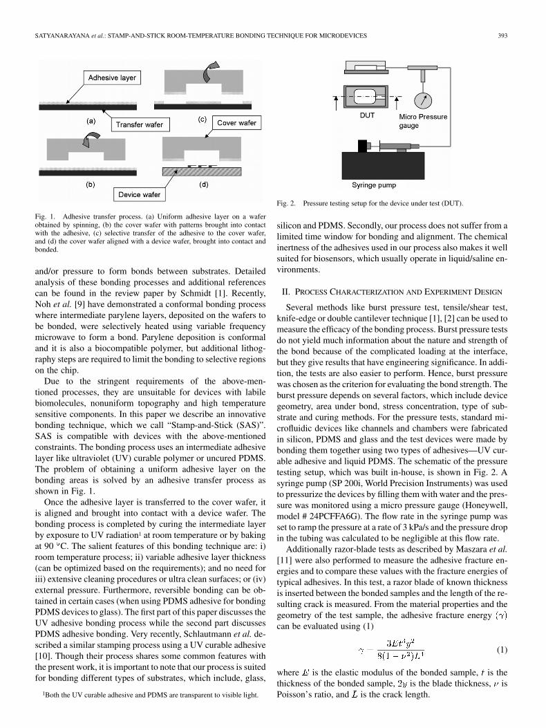
Fig. 2. Pressure testing setup for the device under test (DUT).
silicon and PDMS. Secondly, our process does not suffer from alimited time window for bonding and alignment. The chemicalinertness of the adhesives used in our process also makes it wellsuited for biosensors, which usually operate in liquid/saline en-vironments.
II. PROCESS CHARACTERIZATION AND EXPERIMENT DESIGN
Several methods like burst pressure test, tensile/shear test,knife-edge or double cantilever technique [1], [2] can be used tomeasure the efficacy of the bonding process. Burst pressure testsdo not yield much information about the nature and strength ofthe bond because of the complicated loading at the interface,but they give results that have engineering significance. In addi-tion, the tests are also easier to perform. Hence, burst pressurewas chosen as the criterion for evaluating the bond strength. Theburst pressure depends on several factors, which include devicegeometry, area under bond, stress concentration, type of sub-strate and curing methods. For the pressure tests, standard mi-crofluidic devices like channels and chambers were fabricatedin silicon, PDMS and glass and the test devices were made bybonding them together using two types of adhesives—UV cur-able adhesive and liquid PDMS. The schematic of the pressuretesting setup, which was built in-house, is shown in Fig. 2. Asyringe pump (SP 200i, World Precision Instruments) was usedto pressurize the devices by filling them with water and the pres-sure was monitored using a micro pressure gauge (Honeywell,model # 24PCFFA6G). The flow rate in the syringe pump wasset to ramp the pressure at a rate of 3 kPa/s and the pressure dropin the tubing was calculated to be negligible at this flow rate.
Additionally razor-blade tests as described by Maszara et al.[11] were also performed to measure the adhesive fracture en-ergies and to compare these values with the fracture energies oftypical adhesives. In this test, a razor blade of known thicknessis inserted between the bonded samples and the length of the re-sulting crack is measured. From the material properties and thegeometry of the test sample, the adhesive fracture energycan be evaluated using (1)
(1)
where is the elastic modulus of the bonded sample, is thethickness of the bonded sample, is the blade thickness, isPoisson’s ratio, and is the crack length.
394 JOURNAL OF MICROELECTROMECHANICAL SYSTEMS, VOL. 14, NO. 2, APRIL 2005
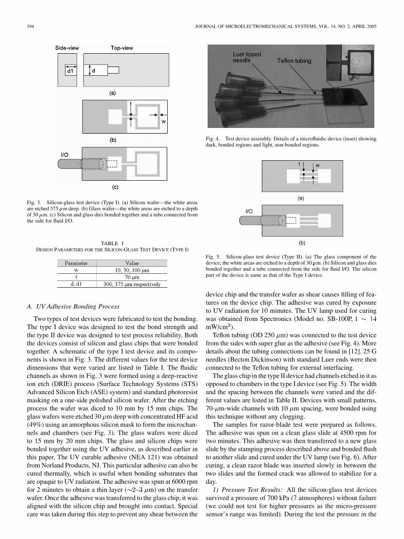
Fig. 3. Silicon-glass test device (Type I). (a) Silicon wafer—the white areasare etched 375 �m deep. (b) Glass wafer—the white areas are etched to a depthof 30 �m. (c) Silicon and glass dies bonded together and a tube connected fromthe side for fluid I/O.
TABLE IDESIGN PARAMETERS FOR THE SILICON-GLASS TEST DEVICE (TYPE I)
A. UV Adhesive Bonding Process
Two types of test devices were fabricated to test the bonding.The type I device was designed to test the bond strength andthe type II device was designed to test process reliability. Boththe devices consist of silicon and glass chips that were bondedtogether. A schematic of the type I test device and its compo-nents is shown in Fig. 3. The different values for the test devicedimensions that were varied are listed in Table I. The fluidicchannels as shown in Fig. 3 were formed using a deep-reactiveion etch (DRIE) process (Surface Technology Systems (STS)Advanced Silicon Etch (ASE) system) and standard photoresistmasking on a one-side polished silicon wafer. After the etchingprocess the wafer was diced to 10 mm by 15 mm chips. Theglass wafers were etched 30 m deep with concentrated HF acid(49%) using an amorphous silicon mask to form the microchan-nels and chambers (see Fig. 3). The glass wafers were dicedto 15 mm by 20 mm chips. The glass and silicon chips werebonded together using the UV adhesive, as described earlier inthis paper. The UV curable adhesive (NEA 121) was obtainedfrom Norland Products, NJ. This particular adhesive can also becured thermally, which is useful when bonding substrates thatare opaque to UV radiation. The adhesive was spun at 6000 rpmfor 2 minutes to obtain a thin layer ( – m) on the transferwafer. Once the adhesive was transferred to the glass chip, it wasaligned with the silicon chip and brought into contact. Specialcare was taken during this step to prevent any shear between the
Fig. 4. Test device assembly. Details of a microfluidic device (inset) showingdark, bonded regions and light, non-bonded regions.
Fig. 5. Silicon-glass test device (Type II). (a) The glass component of thedevice; the white areas are etched to a depth of 30 �m. (b) Silicon and glass diesbonded together and a tube connected from the side for fluid I/O. The siliconpart of the device is same as that of the Type I device.
device chip and the transfer wafer as shear causes filling of fea-tures on the device chip. The adhesive was cured by exposureto UV radiation for 10 minutes. The UV lamp used for curingwas obtained from Spectronics (Model no. SB-100P,mW/cm ).
Teflon tubing (OD 250 m) was connected to the test devicefrom the sides with super glue as the adhesive (see Fig. 4). Moredetails about the tubing connections can be found in [12]. 25 Gneedles (Becton Dickinson) with standard Luer ends were thenconnected to the Teflon tubing for external interfacing.
The glass chip in the type II device had channels etched in it asopposed to chambers in the type I device (see Fig. 5). The widthand the spacing between the channels were varied and the dif-ferent values are listed in Table II. Devices with small patterns,70- m-wide channels with 10 m spacing, were bonded usingthis technique without any clogging.
The samples for razor-blade test were prepared as follows.The adhesive was spun on a clean glass slide at 4500 rpm fortwo minutes. This adhesive was then transferred to a new glassslide by the stamping process described above and bonded flushto another slide and cured under the UV lamp (see Fig. 6). Aftercuring, a clean razor blade was inserted slowly in between thetwo slides and the formed crack was allowed to stabilize for aday.
1) Pressure Test Results: All the silicon-glass test devicessurvived a pressure of 700 kPa (7 atmospheres) without failure(we could not test for higher pressures as the micro-pressuresensor’s range was limited). During the test the pressure in the
SATYANARAYANA et al.: STAMP-AND-STICK ROOM-TEMPERATURE BONDING TECHNIQUE FOR MICRODEVICES 395
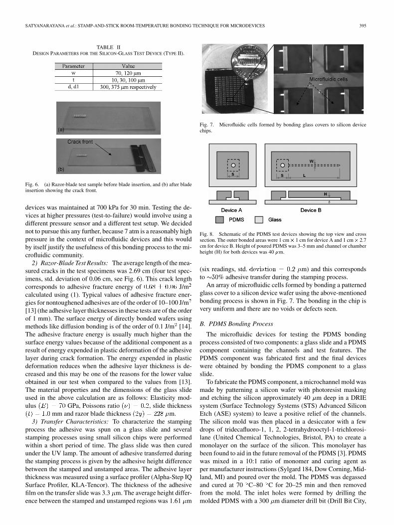
TABLE IIDESIGN PARAMETERS FOR THE SILICON-GLASS TEST DEVICE (TYPE II).
Fig. 6. (a) Razor-blade test sample before blade insertion, and (b) after bladeinsertion showing the crack front.
devices was maintained at 700 kPa for 30 min. Testing the de-vices at higher pressures (test-to-failure) would involve using adifferent pressure sensor and a different test setup. We decidednot to pursue this any further, because 7 atm is a reasonably highpressure in the context of microfluidic devices and this wouldby itself justify the usefulness of this bonding process to the mi-crofluidic community.
2) Razor-Blade Test Results: The average length of the mea-sured cracks in the test specimens was 2.69 cm (four test spec-imens, std. deviation of 0.06 cm, see Fig. 6). This crack lengthcorresponds to adhesive fracture energy of J/mcalculated using (1). Typical values of adhesive fracture ener-gies for nontoughened adhesives are of the order of 10–100 J/m[13] (the adhesive layer thicknesses in these tests are of the orderof 1 mm). The surface energy of directly bonded wafers usingmethods like diffusion bonding is of the order of 0.1 J/m [14].The adhesive fracture energy is usually much higher than thesurface energy values because of the additional component as aresult of energy expended in plastic deformation of the adhesivelayer during crack formation. The energy expended in plasticdeformation reduces when the adhesive layer thickness is de-creased and this may be one of the reasons for the lower valueobtained in our test when compared to the values from [13].The material properties and the dimensions of the glass slideused in the above calculation are as follows: Elasticity mod-ulus GPa, Poissons ratio , slide thickness
mm and razor blade thickness m.3) Transfer Characteristics: To characterize the stamping
process the adhesive was spun on a glass slide and severalstamping processes using small silicon chips were performedwithin a short period of time. The glass slide was then curedunder the UV lamp. The amount of adhesive transferred duringthe stamping process is given by the adhesive height differencebetween the stamped and unstamped areas. The adhesive layerthickness was measured using a surface profiler (Alpha-Step IQSurface Profiler, KLA-Tencor). The thickness of the adhesivefilm on the transfer slide was 3.3 m. The average height differ-ence between the stamped and unstamped regions was 1.61 m
Fig. 7. Microfluidic cells formed by bonding glass covers to silicon devicechips.
Fig. 8. Schematic of the PDMS test devices showing the top view and crosssection. The outer bonded areas were 1 cm� 1 cm for device A and 1 cm� 2.7cm for device B. Height of poured PDMS was 3–5 mm and channel or chamberheight (H) for both devices was 40 �m.
(six readings, std. m) and this correspondsto % adhesive transfer during the stamping process.
An array of microfluidic cells formed by bonding a patternedglass cover to a silicon device wafer using the above-mentionedbonding process is shown in Fig. 7. The bonding in the chip isvery uniform and there are no voids or defects seen.
B. PDMS Bonding Process
The microfluidic devices for testing the PDMS bondingprocess consisted of two components: a glass slide and a PDMScomponent containing the channels and test features. ThePDMS component was fabricated first and the final deviceswere obtained by bonding the PDMS component to a glassslide.
To fabricate the PDMS component, a microchannel mold wasmade by patterning a silicon wafer with photoresist maskingand etching the silicon approximately 40 m deep in a DRIEsystem (Surface Technology Systems (STS) Advanced SiliconEtch (ASE) system) to leave a positive relief of the channels.The silicon mold was then placed in a desiccator with a fewdrops of tridecafluoro-1, 1, 2, 2-tetrahydrooctyl-1-trichlorosi-lane (United Chemical Technologies, Bristol, PA) to create amonolayer on the surface of the silicon. This monolayer hasbeen found to aid in the future removal of the PDMS [3]. PDMSwas mixed in a 10:1 ratio of monomer and curing agent asper manufacturer instructions (Sylgard 184, Dow Corning, Mid-land, MI) and poured over the mold. The PDMS was degassedand cured at 70 C–80 C for 20–25 min and then removedfrom the mold. The inlet holes were formed by drilling themolded PDMS with a 300 m diameter drill bit (Drill Bit City,
396 JOURNAL OF MICROELECTROMECHANICAL SYSTEMS, VOL. 14, NO. 2, APRIL 2005
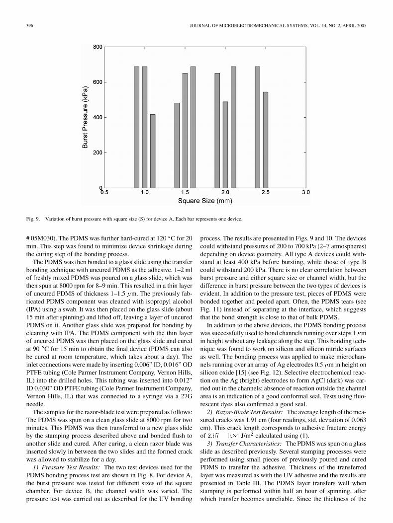
Fig. 9. Variation of burst pressure with square size (S) for device A. Each bar represents one device.
# 05M030). The PDMS was further hard-cured at 120 C for 20min. This step was found to minimize device shrinkage duringthe curing step of the bonding process.
The PDMS was then bonded to a glass slide using the transferbonding technique with uncured PDMS as the adhesive. 1–2 mlof freshly mixed PDMS was poured on a glass slide, which wasthen spun at 8000 rpm for 8–9 min. This resulted in a thin layerof uncured PDMS of thickness 1–1.5 m. The previously fab-ricated PDMS component was cleaned with isopropyl alcohol(IPA) using a swab. It was then placed on the glass slide (about15 min after spinning) and lifted off, leaving a layer of uncuredPDMS on it. Another glass slide was prepared for bonding bycleaning with IPA. The PDMS component with the thin layerof uncured PDMS was then placed on the glass slide and curedat 90 C for 15 min to obtain the final device (PDMS can alsobe cured at room temperature, which takes about a day). Theinlet connections were made by inserting 0.006” ID, 0.016” ODPTFE tubing (Cole Parmer Instrument Company, Vernon Hills,IL) into the drilled holes. This tubing was inserted into 0.012”ID 0.030” OD PTFE tubing (Cole Parmer Instrument Company,Vernon Hills, IL) that was connected to a syringe via a 27Gneedle.
The samples for the razor-blade test were prepared as follows:The PDMS was spun on a clean glass slide at 8000 rpm for twominutes. This PDMS was then transferred to a new glass slideby the stamping process described above and bonded flush toanother slide and cured. After curing, a clean razor blade wasinserted slowly in between the two slides and the formed crackwas allowed to stabilize for a day.
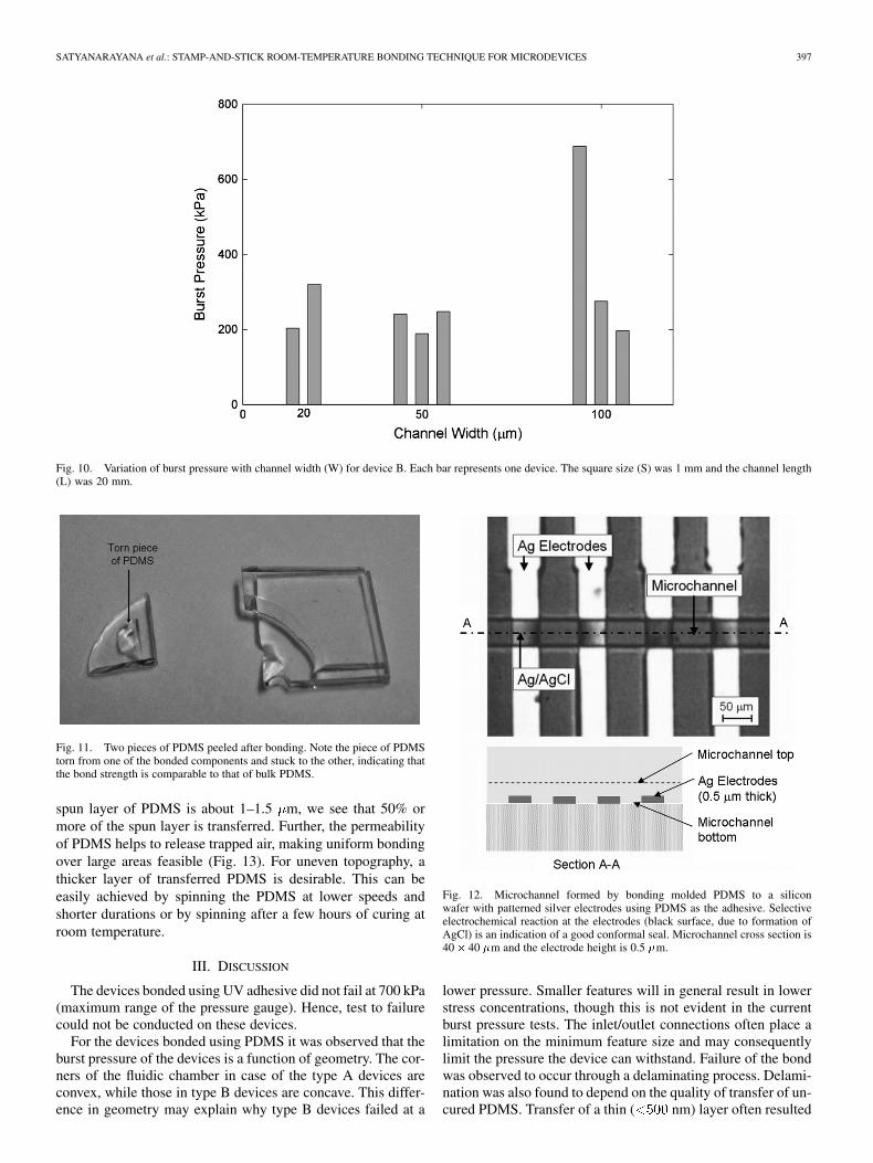
1) Pressure Test Results: The two test devices used for thePDMS bonding process test are shown in Fig. 8. For device A,the burst pressure was tested for different sizes of the squarechamber. For device B, the channel width was varied. Thepressure test was carried out as described for the UV bonding
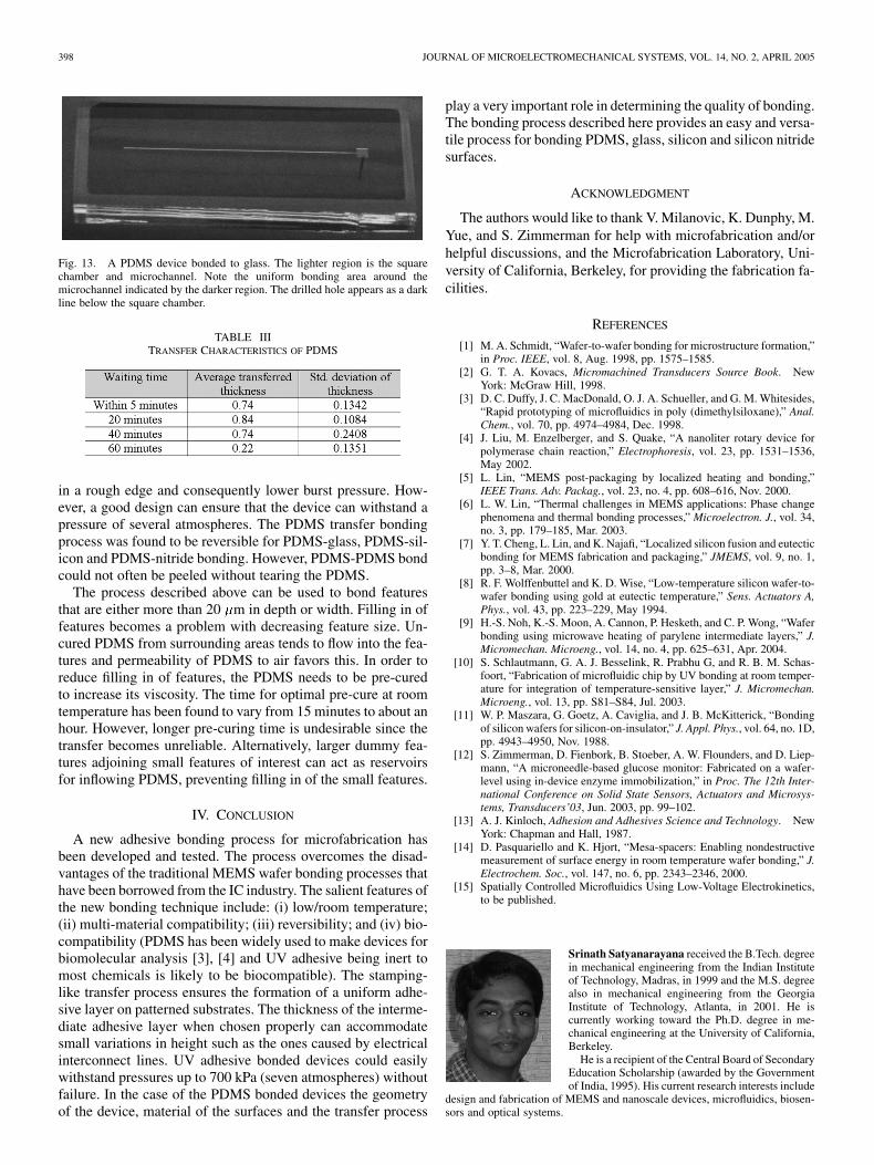
process. The results are presented in Figs. 9 and 10. The devicescould withstand pressures of 200 to 700 kPa (2–7 atmospheres)depending on device geometry. All type A devices could with-stand at least 400 kPa before bursting, while those of type Bcould withstand 200 kPa. There is no clear correlation betweenburst pressure and either square size or channel width, but thedifference in burst pressure between the two types of devices isevident. In addition to the pressure test, pieces of PDMS werebonded together and peeled apart. Often, the PDMS tears (seeFig. 11) instead of separating at the interface, which suggeststhat the bond strength is close to that of bulk PDMS.
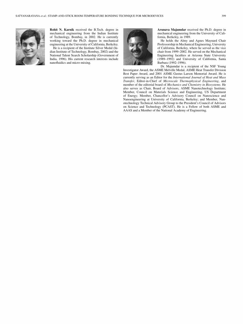
In addition to the above devices, the PDMS bonding processwas successfully used to bond channels running over steps 1 min height without any leakage along the step. This bonding tech-nique was found to work on silicon and silicon nitride surfacesas well. The bonding process was applied to make microchan-nels running over an array of Ag electrodes 0.5 m in height onsilicon oxide [15] (see Fig. 12). Selective electrochemical reac-tion on the Ag (bright) electrodes to form AgCl (dark) was car-ried out in the channels; absence of reaction outside the channelarea is an indication of a good conformal seal. Tests using fluo-rescent dyes also confirmed a good seal.
2) Razor-Blade Test Results: The average length of the mea-sured cracks was 1.91 cm (four readings, std. deviation of 0.063cm). This crack length corresponds to adhesive fracture energyof J/m calculated using (1).
3) Transfer Characteristics: The PDMS was spun on a glassslide as described previously. Several stamping processes wereperformed using small pieces of previously poured and curedPDMS to transfer the adhesive. Thickness of the transferredlayer was measured as with the UV adhesive and the results arepresented in Table III. The PDMS layer transfers well whenstamping is performed within half an hour of spinning, afterwhich transfer becomes unreliable. Since the thickness of the
SATYANARAYANA et al.: STAMP-AND-STICK ROOM-TEMPERATURE BONDING TECHNIQUE FOR MICRODEVICES 397
Fig. 10. Variation of burst pressure with channel width (W) for device B. Each bar represents one device. The square size (S) was 1 mm and the channel length(L) was 20 mm.
Fig. 11. Two pieces of PDMS peeled after bonding. Note the piece of PDMStorn from one of the bonded components and stuck to the other, indicating thatthe bond strength is comparable to that of bulk PDMS.
spun layer of PDMS is about 1–1.5 m, we see that 50% ormore of the spun layer is transferred. Further, the permeabilityof PDMS helps to release trapped air, making uniform bondingover large areas feasible (Fig. 13). For uneven topography, athicker layer of transferred PDMS is desirable. This can beeasily achieved by spinning the PDMS at lower speeds andshorter durations or by spinning after a few hours of curing atroom temperature.
III. DISCUSSION
The devices bonded using UV adhesive did not fail at 700 kPa(maximum range of the pressure gauge). Hence, test to failurecould not be conducted on these devices.
For the devices bonded using PDMS it was observed that theburst pressure of the devices is a function of geometry. The cor-ners of the fluidic chamber in case of the type A devices areconvex, while those in type B devices are concave. This differ-ence in geometry may explain why type B devices failed at a
Fig. 12. Microchannel formed by bonding molded PDMS to a siliconwafer with patterned silver electrodes using PDMS as the adhesive. Selectiveelectrochemical reaction at the electrodes (black surface, due to formation ofAgCl) is an indication of a good conformal seal. Microchannel cross section is40� 40 �m and the electrode height is 0.5 �m.
lower pressure. Smaller features will in general result in lowerstress concentrations, though this is not evident in the currentburst pressure tests. The inlet/outlet connections often place alimitation on the minimum feature size and may consequentlylimit the pressure the device can withstand. Failure of the bondwas observed to occur through a delaminating process. Delami-nation was also found to depend on the quality of transfer of un-cured PDMS. Transfer of a thin ( nm) layer often resulted
398 JOURNAL OF MICROELECTROMECHANICAL SYSTEMS, VOL. 14, NO. 2, APRIL 2005
Fig. 13. A PDMS device bonded to glass. The lighter region is the squarechamber and microchannel. Note the uniform bonding area around themicrochannel indicated by the darker region. The drilled hole appears as a darkline below the square chamber.
TABLE IIITRANSFER CHARACTERISTICS OF PDMS
in a rough edge and consequently lower burst pressure. How-ever, a good design can ensure that the device can withstand apressure of several atmospheres. The PDMS transfer bondingprocess was found to be reversible for PDMS-glass, PDMS-sil-icon and PDMS-nitride bonding. However, PDMS-PDMS bondcould not often be peeled without tearing the PDMS.
The process described above can be used to bond featuresthat are either more than 20 m in depth or width. Filling in offeatures becomes a problem with decreasing feature size. Un-cured PDMS from surrounding areas tends to flow into the fea-tures and permeability of PDMS to air favors this. In order toreduce filling in of features, the PDMS needs to be pre-curedto increase its viscosity. The time for optimal pre-cure at roomtemperature has been found to vary from 15 minutes to about anhour. However, longer pre-curing time is undesirable since thetransfer becomes unreliable. Alternatively, larger dummy fea-tures adjoining small features of interest can act as reservoirsfor inflowing PDMS, preventing filling in of the small features.
IV. CONCLUSION
A new adhesive bonding process for microfabrication hasbeen developed and tested. The process overcomes the disad-vantages of the traditional MEMS wafer bonding processes thathave been borrowed from the IC industry. The salient features ofthe new bonding technique include: (i) low/room temperature;(ii) multi-material compatibility; (iii) reversibility; and (iv) bio-compatibility (PDMS has been widely used to make devices forbiomolecular analysis [3], [4] and UV adhesive being inert tomost chemicals is likely to be biocompatible). The stamping-like transfer process ensures the formation of a uniform adhe-sive layer on patterned substrates. The thickness of the interme-diate adhesive layer when chosen properly can accommodatesmall variations in height such as the ones caused by electricalinterconnect lines. UV adhesive bonded devices could easilywithstand pressures up to 700 kPa (seven atmospheres) withoutfailure. In the case of the PDMS bonded devices the geometryof the device, material of the surfaces and the transfer process
play a very important role in determining the quality of bonding.The bonding process described here provides an easy and versa-tile process for bonding PDMS, glass, silicon and silicon nitridesurfaces.
ACKNOWLEDGMENT
The authors would like to thank V. Milanovic, K. Dunphy, M.Yue, and S. Zimmerman for help with microfabrication and/orhelpful discussions, and the Microfabrication Laboratory, Uni-versity of California, Berkeley, for providing the fabrication fa-cilities.
REFERENCES
[1] M. A. Schmidt, “Wafer-to-wafer bonding for microstructure formation,”in Proc. IEEE, vol. 8, Aug. 1998, pp. 1575–1585.
[2] G. T. A. Kovacs, Micromachined Transducers Source Book. NewYork: McGraw Hill, 1998.
[3] D. C. Duffy, J. C. MacDonald, O. J. A. Schueller, and G. M. Whitesides,“Rapid prototyping of microfluidics in poly (dimethylsiloxane),” Anal.Chem., vol. 70, pp. 4974–4984, Dec. 1998.
[4] J. Liu, M. Enzelberger, and S. Quake, “A nanoliter rotary device forpolymerase chain reaction,” Electrophoresis, vol. 23, pp. 1531–1536,May 2002.
[5] L. Lin, “MEMS post-packaging by localized heating and bonding,”IEEE Trans. Adv. Packag., vol. 23, no. 4, pp. 608–616, Nov. 2000.
[6] L. W. Lin, “Thermal challenges in MEMS applications: Phase changephenomena and thermal bonding processes,” Microelectron. J., vol. 34,no. 3, pp. 179–185, Mar. 2003.
[7] Y. T. Cheng, L. Lin, and K. Najafi, “Localized silicon fusion and eutecticbonding for MEMS fabrication and packaging,” JMEMS, vol. 9, no. 1,pp. 3–8, Mar. 2000.
[8] R. F. Wolffenbuttel and K. D. Wise, “Low-temperature silicon wafer-to-wafer bonding using gold at eutectic temperature,” Sens. Actuators A,Phys., vol. 43, pp. 223–229, May 1994.
[9] H.-S. Noh, K.-S. Moon, A. Cannon, P. Hesketh, and C. P. Wong, “Waferbonding using microwave heating of parylene intermediate layers,” J.Micromechan. Microeng., vol. 14, no. 4, pp. 625–631, Apr. 2004.
[10] S. Schlautmann, G. A. J. Besselink, R. Prabhu G, and R. B. M. Schas-foort, “Fabrication of microfluidic chip by UV bonding at room temper-ature for integration of temperature-sensitive layer,” J. Micromechan.Microeng., vol. 13, pp. S81–S84, Jul. 2003.
[11] W. P. Maszara, G. Goetz, A. Caviglia, and J. B. McKitterick, “Bondingof silicon wafers for silicon-on-insulator,” J. Appl. Phys., vol. 64, no. 1D,pp. 4943–4950, Nov. 1988.
[12] S. Zimmerman, D. Fienbork, B. Stoeber, A. W. Flounders, and D. Liep-mann, “A microneedle-based glucose monitor: Fabricated on a wafer-level using in-device enzyme immobilization,” in Proc. The 12th Inter-national Conference on Solid State Sensors, Actuators and Microsys-tems, Transducers’03, Jun. 2003, pp. 99–102.
[13] A. J. Kinloch, Adhesion and Adhesives Science and Technology. NewYork: Chapman and Hall, 1987.
[14] D. Pasquariello and K. Hjort, “Mesa-spacers: Enabling nondestructivemeasurement of surface energy in room temperature wafer bonding,” J.Electrochem. Soc., vol. 147, no. 6, pp. 2343–2346, 2000.
[15] Spatially Controlled Microfluidics Using Low-Voltage Electrokinetics,to be published.
Srinath Satyanarayana received the B.Tech. degreein mechanical engineering from the Indian Instituteof Technology, Madras, in 1999 and the M.S. degreealso in mechanical engineering from the GeorgiaInstitute of Technology, Atlanta, in 2001. He iscurrently working toward the Ph.D. degree in me-chanical engineering at the University of California,Berkeley.
He is a recipient of the Central Board of SecondaryEducation Scholarship (awarded by the Governmentof India, 1995). His current research interests include
design and fabrication of MEMS and nanoscale devices, microfluidics, biosen-sors and optical systems.
SATYANARAYANA et al.: STAMP-AND-STICK ROOM-TEMPERATURE BONDING TECHNIQUE FOR MICRODEVICES 399
Rohit N. Karnik received the B.Tech. degree inmechanical engineering from the Indian Instituteof Technology, Bombay, in 2002. He is currentlyworking toward the Ph.D. degree in mechanicalengineering at the University of California, Berkeley.
He is a recipient of the Institute Silver Medal (In-dian Institute of Technology, Bombay, 2002) and theNational Talent Search Scholarship (Government ofIndia, 1996). His current research interests includenanofluidics and micro-mixing.
Arunava Majumdar received the Ph.D. degree inmechanical engineering from the University of Cali-fornia, Berkeley, in 1989.
He holds the Almy and Agnes Maynard ChairProfessorship in Mechanical Engineering, Universityof California, Berkeley, where he served as the vicechair from 1999–2002. He served on the MechanicalEngineering faculties at Arizona State University(1989–1992) and University of California, SantaBarbara (1992–1996).
Dr. Majumdar is a recipient of the NSF YoungInvestigator Award, the ASME Melville Medal, ASME Heat Transfer DivisionBest Paper Award, and 2001 ASME Gustus Larson Memorial Award. He iscurrently serving as an Editor for the International Journal of Heat and MassTransfer, Editor-in-Chief of Microscale Thermophysical Engineering, andmember of the editorial board of Mechanics and Chemistry in Biosystems. Healso serves as Chair, Board of Advisors, ASME Nanotechnology Institute;Member, Council on Materials Science and Engineering, US Departmentof Energy; Member, Chancellor’s Advisory Council on Nanoscience andNanoengineering at University of California, Berkeley; and Member, Nan-otechnology Technical Advisory Group to the President’s Council of Advisorson Science and Technology (PCAST). He is a Fellow of both ASME andAAAS and a Member of the National Academy of Engineering.