42
1 3D and SOI Technology for Future Pixel Detectors Ray Yarema Fermilab Common ATLAS CMS Electronics Workshop At CERN March 19-21, 2007

1
3D and SOI Technology for Future Pixel Detectors
Ray YaremaFermilab
Common ATLAS CMS Electronics WorkshopAt CERN
March 19-21, 2007

2
Introduction• Requirements for HEP pixel electronics and detectors continue to
push the limits for lower mass and power, and higher resolution.• Significant progress has been made to address these issues by
integrating sensors and front end electronics within the pixel cell.– Monolithic Active Pixel Sensors (MAPS)
• Much has been accomplished but there are fundamental limitationsto this approach
– Small signal dependent on epi thickness– Most designs are limited to NMOS transistors (limited functionality)– Slow rise time set by diffusion
– There are other choices under development• SOI (Silicon on Insulator) Pixel Sensors
– Offers improvements over MAPS• 3D integrated circuits
– Offers improved performance over SOI pixel sensors.
Metal layersPolysilicon
N+P+ WellN+ Well
P- epi
P++ substrate
- +- +
- +- +
- +- +
- +- +
- +
5-20 um
Particle
Sensing Diode
3 NMOS trans. in pixel

3
Active Pixel Sensor in SOIPMOS andNMOStransistors
Detector signalIs proportional To substrate thickness
Thin top layer has silicon islands in which PMOS and NMOS transistors are built.A buried oxide layer (BOX) separates the top layer from the substrate.The high resistivity substrate forms the detector volume.The diode implants are formed beneath the BOX and connected by vias.The raw SOI wafers are procured from commercial vendors such as SOITEC in France.
Advantages:* 100% fill factor* NMOS + PMOS transistors* Large signal* Faster charge collection
Charge releasedalong track
Buried oxide200 nm

4
Fermilab SOI Detector ActivitiesSOI detector development is being pursued by Fermilab at two different foundries :OKI in Japan, and American Semiconductor Inc. (ASI) in US . The two processes have different characteristics as seen below
Thinned to 350 μm, no contact processing, plated with Al (200 nm).
Backside
Wafer Diameter: 150 mmφ, Top Si : Cz, ~18 Ω-cm, p-type, ~40 nm thick Buried Oxide: 200 nm thickHandle wafer: Cz、>1k Ω-cm (No type assignment), 650 μm thick (SOITEC)
SOI wafer
0.15μm Fully-Depleted SOI CMOSprocess, 1 Poly, 5 Metal layers (OKI Electric Industry Co. Ltd.).
Process
Thinned to 50-100 μm, polished, laser annealed and plated with Al.
Backside
Wafer Diameter: 200 mmφ, Handle wafer: FZ>1k Ω-cm(n type)
SOI wafer
0.18μm partially-Depleted dual gate SOI CMOS process,Dual gate transistor (Flexfet),No poly, 5 metal (American Semicondutor /
Cypress Semiconductor.)
Process
OKI Process ASI Process

5
OKI Process• KEK has organized two
multi-project wafer (MPW) runs at the OKI foundry. 1– Second MPW run has 17
designs from 7 different organizations.
• Chips due back in March– A 3rd run is planned for
later this year• First SOI Detector
Workshop took place March 6, 2007 at KEK.
Reticule for 2nd OKI MPW run

6
Fermilab Pixel Design in OKI Process• A chip has been designed in the OKI 0.15 micron
process to understand the advantages and problems of SOI detector design. 2– The chip is a wide dynamic range counting pixel
detector chip that is sensitive to 100-400 KeVelectrons, high energy X-rays, and minimum ionizing particles.
• Issues uncovered– Trapped charge in the BOX due to radiation can be a
problem in high radiation applications.• The radiation induced threshold shift can be
corrected by changing the voltage on the substrate.3
– The back gate effect, which appears in detector applications, is an important design consideration in the OKI process.

7
Back gate Effect in OKI Process1
BOXN+ N+P P+ P+N
InOut
Back gate
Silicon Substrate
The threshold shift problem exists for SOItransistors in processes like OKI which have a floating body. The ASI process has a discrete back gate which shields the transistor from the substrate and thus eliminates the problem.
Substrate voltage acts as a back gatebias and changes transistor threshold
Inverter signal disappearswhen back gate voltage = 16 V.
[email protected](STD6)
Inverter
Inverter response to back gate

8
Back Gate Voltage Control
EquipotentialLines
P+ P+ P+N substrate
Transistors
High potential under thistransistor causes large Vt shift
+VbiasSmallspacing
Largespacing
Diodeimplant
To reduce voltage under the transistors, keep P+ implants close together.
Increasingvoltage

9
• Counting pixel detector plus readout circuit– Maximum counting rate ~ 1 MHz/pixel.
• Simplified architecture due to design time constraint– Reconfigurable counter/shift register
• 12 bit dynamic range– Limited peripheral circuitry
• Drivers and bias generator• Array size 64x64 pixels• 350 micron detector thickness
Fermilab MPW Pixel Design for OKI
Amplifier Shaper Discriminator 12bit Counter
10
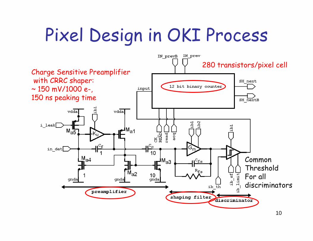
Pixel Design in OKI Process
Charge Sensitive Preamplifierwith CRRC shaper:
~ 150 mV/1000 e-,150 ns peaking time
280 transistors/pixel cell
CommonThresholdFor alldiscriminators

11
Simplified 3 x 3 Pixel Matrix
Operates in twomodes: Acquire/Read out
12 bit counter is reset by changing counter to a shift register configuration andshifting in zeros during read out.

12
OKI Pixel Detector Cross Section
13 umFour equally spaced diodes are used in each pixel to minimizethe effect of back gate voltageby keeping the implant spacingsmall (13 microns).
13 um
P+ implant spacing

13
Pixel Cell LayoutOne of fourdetector diodes
One of twelveD flip-flopsarranged aroundperimeter of pixelcell
All analogcircuits arelocated in center of pixel cellbetweendiodes and surroundedby guardring
26 microns

14
4K Pixel Design in OKI ProcessChip name isMAMBO:
Monolithic Activepixel Matrix withBinary cOunters
Chip size:64 x 64 array2.5 mm x 2.5 mm
Designed byGregory Deptuch
Chip due in March.Will examine crosstalk issuesand check radtolerance.

15
ASI Process• ASI process based on dual gate transistor called a
Flexfet.4– Flexfet has a top and bottom gate.– Bottom gate shields the transistor channel from charge build
up in the BOX caused by radiation.– Bottom gate also shields the transistor channel from voltage
on the substrate and thus removes the back gate voltage problem.

16
Design in ASI Process• US Department of Energy
Small Business Innovation Research (SBIR) phase 1 funding
• Modeling and process simulation of a thinned, fully depleted sensor/readout device.
• Studies of backside thinning, implantation, and laser annealing.
• Circuit design for ILC vertex detector in progress. Diode simulation in Flexfet process

17
Vertical Scale Integration (3D)• SOI detector technology offers several
advantages over MAPS.• 3D offers advantages over SOI detectors
– Increased circuit density due to multiple tiers of electronics
– Independent control of substrate materials for each of the tiers.
– Ability to mate various technologies in a monolithic assembly
• DEPFET + CMOS or SOI• CCD + CMOS or SOI• MAPS + CMOS or SOI
Opto Electronicsand/or Voltage Regulation
Digital Layer
Analog Layer
Sensor Layer
Physicist’s Dream
50 um
Power In
Optical In Optical Out

18
3D Integrated Circuits• A 3D chip is generally referred to as a chip comprised
of 2 or more layers of active semiconductor devices that have been thinned, bonded, and interconnected to form a “monolithic” circuit.
• Often the layers (sometimes called tiers) are fabricated in different processes.
• Industry is moving toward 3D to improve circuit performance. (Performance limited by interconnect)– Reduce R, L, C for higher speed– Reduce chip I/O pads– Provide increased functionality– Reduce interconnect power and crosstalk
• HEP should watch industry and take advantage of the technology when applicable.
• Numerous examples of industry produced devices.5,6,7
(See backup slides)
3D Routing (small chip)2D Routing (large chip)

19
Two Different 3D Approaches for HEP
• Die to Wafer bonding– Permits use of different size wafers– Lends itself to using KGD (Known Good Die) for
higher yields• Wafer to Wafer bonding
– Must have same size wafers– Less material handling but lower overall yield
Die to wafer bonding
KGD
Wafer to wafer bonding
Dice/test

20
Key Technologies for 3D• There are 4 key technologies
– Bonding between layers– Wafer thinning– Through wafer via formation and
metalization– High precision alignment
• Many of these technologies are also used in the development of SOI detectors

21
Key Technologies1) Bonding between Die/Wafers
a) Adhesive bond
b) Oxide bond (SiO2 to SiO2)
c) CuSn Eutectic
d) Cu thermocompression
e) DBI (Direct Bond Interconnect)
For (a) and (b), electrical connections between layers areformed after bonding. For (c), (d), and (e), the electricaland mechanical bonds are formed at the same time.
Polymer(BCB)
SiO2bond
Cu SnCu3Sn
(eutectic bond)
CuCubond
MetalOxidebond
Metal bond

22
Key Technologies
Through wafer vias typically have an 8 to 1 aspect ratio. In order tokeep the area associated with the via as small as possible, the wafers should be thinned as much as possible. Thinning is typically done by acombination of grinding, lapping, and chemical or plasma etching.
2) Wafer thinning
Photos from MIT LL
Six inch wafer thinned to 6 microns and mounted to 3 mil kapton.

23
Key Technologies3) Via formation and metalizationTwo different proceedures are generally used:
Via First - vias holes and via metalization take place on awafer before wafer bonding.
Via Last - vias holes and via metalization take place on awafer after wafer bonding.Vias in CMOS are formed using the Bosch process and must bepassivated before filling with metal while Vias in SOI are formedusing an oxide etch are filled without passivation.
SEM of 3 vias using Bosch process8
Via usingoxide etchprocess(LincolnLabs)
Typical diameters are 1-2 microns

24
Key Technologies4) High Precision Alignment
Alignment for both die to wafer and wafer to wafer bondingis typically better than one micron. (Photos by Ziptronix.)
Die to Wafer alignmentand placement
Wafer to Wafer alignmentand placement

25
3D Pixel Design for ILC Vertex9
• 3D chip design in MIT Lincoln Labs 0.18 um SOI process.– Key features: Analog pulse height, sparse readout, high resolution time stamps.– Time stamping and sparse readout occur in the pixel, Hit address found on array perimeter.
• 64 x 64 pixel demonstrator version of 1k x 1K array.• Submitted to 3 tier multi project run. Sensor to be added later.
X=1
T11 5
Y=1
X=2
T21 5
10 10
Y=2
Y=3
Y address bus
110
cell1:1
cell2:1
cell1:2
cell2:2
cell1:3
X=1000
Token to row Y=2
Token to row Y=3
Serial Data out(30 bits/hit)
DigitalData MuxX,Y,Time
StartReadoutToken
XY
Time
T1buf T2buf
Note: All the Y address registers can be replaced by one counter thatis incremented by the last column token.
cell1000:1
cell2:3
cell1000:2
cell1000:3
Assume 1000 x 1000 arrayX and Y addresses are 10bits each
Analogoutputs

26
Simplified Pixel Cell Block Diagram• When a Hit occurs, the Hit pixel stores Sample 1 & 2 and the
Time Stamp, and sets the Hit Latch in sparse readout circuit.• During readout, when the read out token arrives, the time stamp
and analog values are read out, and pixel points to hit address found on perimeter of chip.
• While outputting data from one pixel, the readout token is passed ahead looking for next pixel that has been hit.
Integrator
Discriminator
Analog out
Timestampcircuit
Test inject
Read allRS
Q Pixelskiplogic
Write data
D FF
Data clk
Readdata
To x, yaddress
T.S.out
Hit latchVth
Analog front end Pixel sparsification circuitry Time stamp
Readout token
S1
S2
Hit

27
Tier 3analog
Tier 2Time Stamp
Tier 1Datasparsification
3D Three TierArrangement for ILC Pixel
3Dvias
Sample1
Sample2 Vth
Sample 1
To analog output buses
S. TrigDelay
Digital time stamp bus5
Pad to sensor
Analog T.S.b0 b1 b2 b3 b4
Analog time output bus
Analog ramp bus
Write data
Read data
Test input S.R.Injectpulse
In
OutSR
Q
Y address
X address
D FF
Pixelskiplogic
Token In
Token out
Readall
Read dataData clk
Tier 1
Tier 2
Tier 3
Chip designers:Tom ZimmermanGregory DeptuchJim Hoff

28
Tier 1 - Sparsification • OR for READ ALL cells• Hit latch (SR FF)• Pixel skip logic for
token passing• D flip flop (static),
conservative design• X, Y line pull down• Register for
programmable test input.
• Could probably add disable pixel feature with little extra space
• 65 transistors• 3 via pads
D FF
X, Y line control
Token passing logic
Test inputcircuit
OR, SR FF
20 µm

29
Tier 2 - Time Stamp • 5 bit digital
time stamp• Analog time
stamp –resolution to be determined by analog offsets and off chip ADC
• Gray code counter on periphery
• 72 transistors• 3 vias
b0
b1
b2
b3
b4
AnalogT. S.
20 µm

30
Tier 3 - Analog • Integrator• Double
correlated sample plus readout
• Discriminator• Chip scale
programmable threshold input
• Capacitive test input
• 38 transistors• 2 vias
IntegratorDiscriminator
DCS + Readout
Schmitt Trigger+NOR
Pad foredgeless detector

31
3D Stack with Vias
High resistivity substrateBOX
Vias: 1.5 um diaby 7.3 um long
Tier 1
Tier 2
Tier 3
Pixel cell:*175 transistors in 20 µm pixel.*Unlimited use of PMOS and NMOS.*Allows 100 % diode fill factor.
Chip is due back inAugust. Issues to bestudied include analogperformance, yield, and radiation tolerance.
20 um
20 um

32
MIT LL 3D Multiproject Run Chip Cross Section
8.2 µm
7.8 µm
6.0 µm
3D viasThree levels of transistors,11 levels ofmetal in atotal verticalheight ofonly 22 um.
The MIT LLprocessdescriptionis given ina backup slide.

33
Possible Application to SLHC Pixels• Future pixel upgrades will look for
– Less mass• Thinner sensors (lower V)• Less copper
– More complexity• Higher readout speed• More functionality
– May want smaller pixels for reduced noise to go along with smaller detector signal.
• Use serial powering for pixel Read Out chip.
• 3D allows for creative solutions, e.g.– Accommodates serial
powering– Higher functionality/area– Thinner assemblies– Allows use of edgeless
detectors
Edgeless Pixel Array
Pixel Cell Electronics
Serial Power
End of column logic
Serial Powering
Wire bondsto adjacentchip
Wire bondsto adjacentchip

34
Edgeless Detector Concept
Equipotential lines in detector nearone detector edge
Detector Cross section nearone detector edge
Implant withlaser annealing
Trench ondetector edge filledwith polyand connectedto bottomimplant
Diode implantsDetectorbias
To otherpixels
20 um

35
Summary• Progress is being made to integrate sensors and readout
electronics in a monolithic structure for pixels.• Commercial foundries are starting to develop SOI detectors and
ROICs.– OKI, ASI, and perhaps Hammamtsu– May have limited radiation tolerance but sufficient for most
applications.• 3D is being pursued by many commercial organizations9
– HEP groups are beginning to look at 3D technologies• MPG in Munich is starting an activity to bond pixel sensors
to ROICs and is looking for interested partners.10
• Group at Strasbourg is starting to look at wafer bonding techniques.11
– Expensive but offers a great deal of design flexibility.– Use of CMOS provides very rad hard parts.– Can be used with a variety of current approaches for vertex
detectors, MAPS, DEPFET, etc.• These new technologies offer new opportunities for difficult
applications that can’t be satisfied with older approaches.

36
Acknowledgements
• I want to thank the designers of the Fermilab chips mentioned in this talk– Grzegorz Deptuch– Jim Hoff– Tom Zimmerman
• And also thank members of the ILC pixel design group at Fermilab for their helpful comments in preparing this talk.

37
References• 1) “SOI Detector R&D: Past & Future”, Y. Arai, et. al, 1st SOI Detector R&D Workshop, KEK,
March 6, 2007.• 2) “SOI Pixel Design at FNAL, Counting Pixel for Imaging”, G. Deptuch, 1st SOI Detector
R&D Workshop, KEK, March 6, 2007.• 3) “SOI Radiation Damage Test and Chip Design”, Y. Ikegami, 1st SOI Detector R&D
Workshop, KEK, March 6, 2007.• 4) “Rad-hard Reconfigurable Bi-Directional Level Shifter (ReBiLS) for NASA Space
applications in the Flexfet 0.18 um SOI CMOS Technology”, K. Degregorio, et. al., 12th NASA Symposium on VLSI Design, Coeur d’Alene, Idaho, USA, Oct. 4-5, 2005.
• 5) “3-D Integration Technology Platform for High Performance Detector Arrays”, D. Temple, et. al., public release from RTI International and DRS Technologies.
• 6) Megapixel CMOS Image Sensor Fabrication in Three-Dimensional Integrated Circuit Technology”, V. Suntharalingam, et. al., ISSCC 2005, pp 356-357.
• 7) Laser Radar Imager Based on 3D Integration of Geiger-Mode Avalanche Photodiodes with Two SOI Timing Circuit Layers”,B. Aull, et. al., ISSCC 2006, pp. 26-27.
• 8) “Through Wafer Via Etching”, A. Chambers, et. al., Advanced Packaging, April 2005.• 9) “Fermilab Initiatives in 3D Integrated Circuits and SOI Design for HEP”, R. Yarema, ILC
Vertex Workshop, Ringberg Castle, Tegernsee, Germany, May 29-31, 2006.• 10) “R&D on thin pixel sensors and a novel interconnection technology for 3D integration of
sensors and electronics”, R. Nisius and Hans-Gunther Moser, Max Planck Gesellschaft, January 19, 2007.
• 11) Private communication with Wojtek Dulinski, March 6, 2007.

38
Back Up Slides

39
RTI 3D Infrared Focal Plane Array
3 Tier circuit diagram
Infrared image
Array cross section
Synchronous Charge Removal
+
-+
-
ControlLogic
N BitRipple
Counter. . .
N Bit ParallelDigital Data Out
VCHG
VTRP
VRST
Cint
Cchg
CLK
CTIAOUT
Analog Residual Output
Detector
Analog Components Digital Components
Synchronous Charge Removal
+
-+
-
ControlLogic
N BitRipple
Counter. . .
N Bit ParallelDigital Data Out
VCHG
VTRP
VRST
Cint
Cchg
CLK
CTIAOUT
Analog Residual Output
Detector
Analog Components Digital Components
Diodes0.25 µmCMOS0.18 µmCMOS
Diode
Analog Digital
30 um
• 256 x 256 array with 30 µm pixels
• 3 Tiers– HgCdTe (sensor)– 0.25 µm CMOS
(analog)– 0.18 µm CMOS
(digital)• Die to wafer stacking• Polymer adhesive
bonding• Bosch process vias (4
µm) with insulated side walls
• 99.98% good pixels• High diode fill factor

40
MIT LL3D Megapixel CMOS Image Sensor
• 1024 x 1024, 8 µm pixels• 2 tiers• Wafer to wafer stacking
(150 mm to 150 mm)• 100% diode fill factor• Tier 1 - p+n diodes in
>3000 ohm-cm, n-type sub, 50 µm thick
• Tier 2 – 0.35 um SOI CMOS, 7 µm thick
• 2 µm square vias, dry etch, Ti/TiN liner with W plugs
• Oxide-oxide bonding• 1 million 3D vias• Pixel operability >99.999%• 4 side abuttable array
50 µm
7 µm
Drawing and SEM Cross section
CircuitDiagram
Image
Light

41
MIT LL 3D Laser Radar Imager
Tier 1
Tier 2
Tier 3
7 µm
7 µm
SEM Cross section
CAD DrawingSchematic
64 x 64 array, 30 µm pixels3 tiers
0.18µm SOI0.35 µm SOIHigh resistivity substrate diodes
Oxide to oxide wafer bonding1.5 µm vias, dry etchSix 3D vias per pixel
42
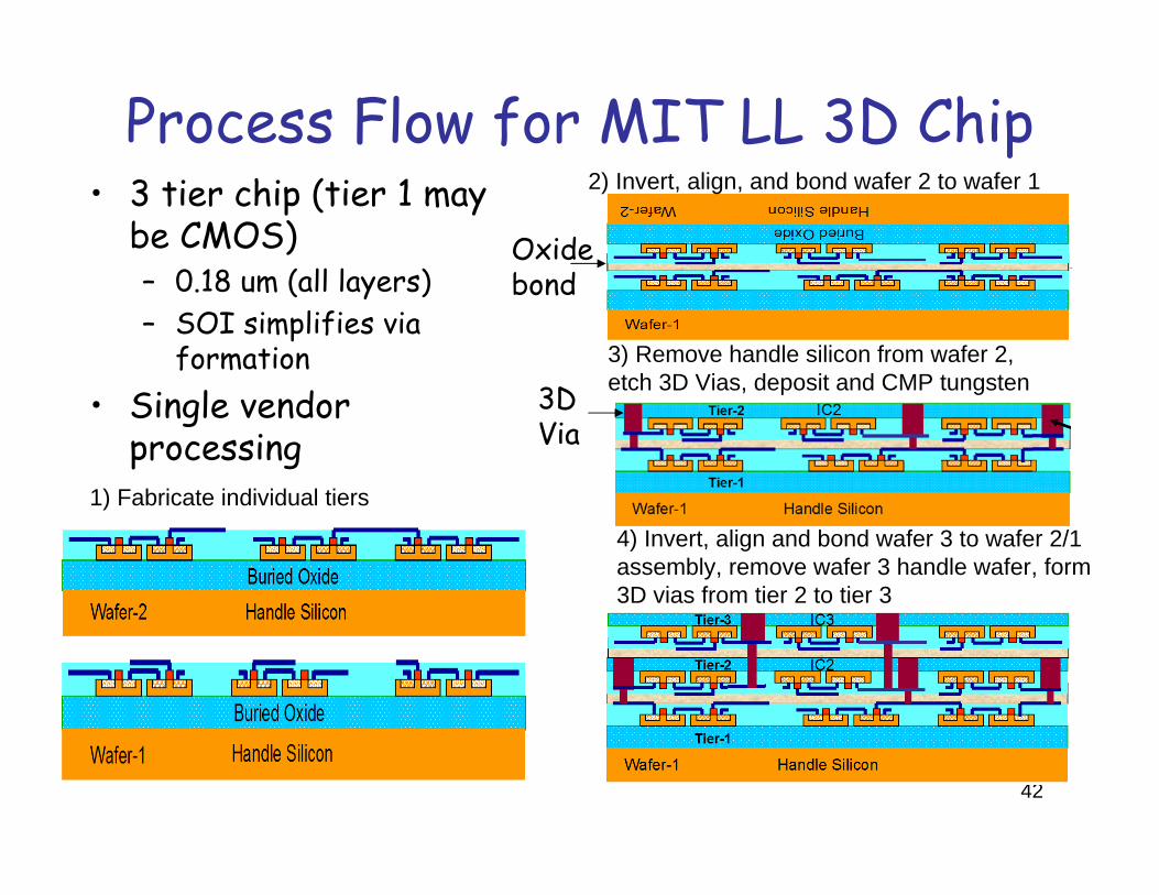
Process Flow for MIT LL 3D Chip• 3 tier chip (tier 1 may
be CMOS)– 0.18 um (all layers)– SOI simplifies via
formation• Single vendor
processing
Oxidebond
3DVia
1) Fabricate individual tiers
2) Invert, align, and bond wafer 2 to wafer 1
3) Remove handle silicon from wafer 2, etch 3D Vias, deposit and CMP tungsten
4) Invert, align and bond wafer 3 to wafer 2/1 assembly, remove wafer 3 handle wafer, form 3D vias from tier 2 to tier 3


