Abstract — This work presents the design, implementation,and characterization of a high-temperature tunable RF oscillatorutilising a developed 3D integration technology. The circuitis based on an in-house fabricated AlGaN/GaN high electronmobility transistor (HEMT) on sapphire that is verticallyintegrated on a custom monolithic microwave integrated circuit(MMIC) on quartz, where the lumped passives componentsare fabricated. The feasibility of the proposed oscillatorand technology is proven up to 300 ºC with frequenciesranging 1000 - 1040 MHz for different bias voltages. To thebest knowledge of the authors, this is the first 3D integrated RFfrequency oscillator circuit characterized at 300 ºC.
Keywords — 3D integration, AlGaN, GaN, HEMT, highfrequency, high temperature, oscillator, semiconductor.
I. INTRODUCTION
Space, automotive or oil and gas exploiting industriesurge for circuits suited for harsh working conditions in orderto reduce the bulky and costly refrigeration systems thatare necessary for conventional circuitry. The developmentof new technologies to fully utilise the properties of widebandgap materials such as SiC, GaAs, and GaN, togetherwith their application to electronic active devices, [1], haspropelled the study of electronic systems capable of operatingin high temperature environments. High frequency circuitsand particularly the design of oscillators is critical forcommunication and sensing devices and is being intensivelystudied for SiC [2], [3] and GaN [4].
In this work, a 1-GHz tunable oscillator based ona 3D on-chip integrated AlGaN/GaN HEMT is designed,implemented and fully characterized on wafer up to 300 ºC.As shown in Fig. 1, the transistor is vertically integrated intothe MMIC circuit of the oscillator and the overall occupiedsurface is 7.2 mm x 7.2 mm.
II. TECHNOLOGY: FABRICATION AND CHARACTERIZATION
In the proposed design, two different technology processesare developed and 3D integrated. On the one hand, the HEMTas the active device, and on the other hand, the inductors andcapacitors as the passive elements. The characteristics of bothneed to be taken into account in the design course.
The used HEMT is a 15 nm barrier (Al0.25GaN/GaN)in-house fabricated transistor. It is grown by a metalorganicvapour phase epitaxy (MOVPE) on sapphire andpresents a two-finger gate with a length and total width
Sapphire
Quartz
MMIC Oscillatorpassives
HEMT
Fig. 1. 3D transistor integration in the proposed oscillator (no to scale).
of 0.7 µm and 100 µm, respectively. The double-fingerstructure forms two cascaded channels that result ina source-gate-drain-gate-source configuration, where the twosources are not interconnected. Two-port measurements areenabled by the inclusion of a pair of GSG pads attachedto the intrinsic transistor. In this manner, the two signalpads correspond to the gate and drain, while one groundpad of each port is connected to one of the sources andalso to each other, as shown in Fig. 2a. In consequence, thetransistor is measured in common-source (CS) configuration.The transistor is fully characterized both in DC and by meansof its S-parameters from room temperature up to 300 ºC inorder to extract its model. The employed Advanced SpiceModel for High Electron Mobility Transistor (ASM-HEMT)is a physics-based model specific for GaN transistors [5] thatallows modelling the temperature dependence of the device.Contrary to other models, it characterizes the behaviour ofthe transistor when a negative bias voltage is applied to thedrain, which is the working region for the chosen topology.For an applied bias voltage of -12 V the transistor presents at300 ºC a power density of 0.84 mW/mm and ft and fmax
equal 10 GHz and 14 GHz, respectively.The passives are designed with another MMIC process
with CMOS compatible dielectrics and metallizations.Metal-Insulator-Metal (MIM) capacitors and thin-filmunderpass circular inductors are developed on a 675 µmquartz substrate. The chosen plasma enhanced chemical vapor
Fig. 2. (a) Layout of the two-finger gate HEMT. (b) Top: Cross-sectionof the circular inductors (no to scale); bottom: schematic of the inductormodel. (c) Measurement and simulation of the inductance. (d) Series resistancedependence on temperature.
deposition (PECVD) dielectric is a 650 nm SiO2 layer andthe top and bottom metals together with the vias consist of amultilayer stack of Ti/Al annealed for 10 minutes at 450 ºCin order to form a temperature-stable alloy. The simplifiedcross-section of an inductor is presented in the top plot inFig. 2b. The total thicknesses of the bottom (M1) and top(M2) metals are 0.5 µm and 1 µm, respectively.
Test capacitors and inductors are measured from 0.2to 20 GHz and across the temperature range from 25 ºCup to 300 ºC. The measurement results for the inductorsare presented in Fig. 2c. It can be observed that closeto the self-resonant frequency a significant diminishing ofthe inductance takes place with the increase of temperature.This is due to an increase of the series resistance ofthe non ideal inductor, as shown in Fig. 2d, where thedependence of the resistance is linear over temperature suchthat R(T ) = α (T−T0)+R0 for T0, α and R0 equal to 25 ºC,0.13 Ω
C , and 54 Ω, respectively. The extracted model for theinductor, represented in the bottom plot in Fig 2b, comprisesa variable series resistance, R(T ), with an invariant nominalinductance, L, placed in parallel with a small capacitance, C3,which is conditioned by the number of turns. C1, C2, R1,and R2 are substrate dependent. The accuracy of the model isdemonstrated in Fig. 2c and Fig. 2d.
III. OSCILLATOR DESIGN
The oscillator design relies on the combination of the twopreviously described technologies and it is achieved in aninnovative manner: the 3D on-chip integration of the transistor.The sapphire wafer is diced and glued on top of the top metalfrom the quartz wafer and gold bonding wires are used inorder to connect the transistor with the rest of the components.
Nevertheless, two factors are to be taken into account. First, thelayout of the transistor with the two source pads requires themto be connected through the circuit. Second, the bonding wiresimply an extra inductance of approximately 1 nH/mm betweenthe transistor and the passives. The minimum achievablesquare size of the diced transistor blocks was 2 mm x 2 mm.Thus, a value of around 3 nH for each bonding wire isestimated.
Furthermore, the oscillator is implemented as a two-portnegative-resistance oscillator [6], as presented in Fig. 3.Including the bonding inductance (in grey), the S-parametersof the network are simulated in order to ensure that thetransistor is potentially unstable for all temperatures, i.e. µ <1where
µ =1− |S22|2
|S11∆S∗22|+ |S12S21|
(1)
∆ = S11S22 − S21S12. (2)
The negative-resistance is achieved in a reverse-channeltopology [7], where the transistor is placed in a CSconfiguration but the drain is biased with a negative DCvoltage becoming electrically the source. In addition, it allowsthe circuit to function with only one DC source since drainand gate share the same bias. In order to maximize thenegative-resistance presented by the two-port network, a seriesfeedback is added in terms of an inductance between thebonding wires from the source pads and ground, L1 and L2.Due to the parallel structure induced by the double sourcepads, the total inductance feedback is halved. Consequently,changes due to the increasing of the series resistance withtemperature are minimized.
The bias-Ts are implemented on-chip in order to avoiduncontrolled variations, they conform the termination networkand form part of the load network. By these means the initialcondition for the oscillation is ensured. The capacitor, C1,placed in the load network acts as a DC blocking readoutcapacitor of the RF signal that goes to the final real load,which corresponds to the 50 Ω of the measuring device. Thiscapacitance is crucial in the matching of the loads and assuresoscillation over all temperatures.
L1L2
G
S
D
ГOUT ГIN
ZOUT
VDD
Bias TeeTerminating
Network
ГT
VDD
VDD
Bias TeeLoad
Network
ГL
ZIN
l
Terminating Network
Load Network
Bias-TD
Bias-T G1
Bias-T G2
Lb1
Lb3Lb2
Lb4
C1
Fig. 3. Schematic of the designed oscillator in a reverse-channel topology.
520
(a) (b)
50 100 150 200 250 300Temperature (°C)
0.99
0.995
1
1.005
1.01
1.015
1.02
Freq
uenc
y (G
Hz)
0
1
2
3
4
5
Out
put P
ower
(dBm
)
MeasurementSimulationOutput Power
(c)
4 6 8 10 12DC Voltage (V)
0.97
0.98
0.99
1
1.01
1.02
1.03
1.04
Freq
uenc
y (G
Hz)
-8
-6
-4
-2
0
2
4
6
Out
put P
ower
(dBm
)
100ºC200ºC300ºCPower @300ºC
- - - - -
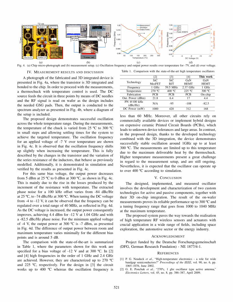
(d)Fig. 4. (a) Chip micro-photograph and (b) measurement setup. (c) Oscillation frequency and output power results over temperature for -7V, and (d) over voltage.
IV. MEASUREMENT RESULTS AND DISCUSSION
A photograph of the fabricated and 3D integrated device ispresented in Fig. 4a, where the transistor is 3D integrated andbonded to the chip. In order to proceed with the measurements,a thermochuck with temperature control is used. The DCsource feeds the circuit in three points by means of DC needlesand the RF signal is read on wafer as the design includesthe needed GSG pads. Then, the output is conducted to thespectrum analyzer as presented in Fig. 4b, where a diagram ofthe setup is included.
The proposed design demonstrates successful oscillationacross the whole temperature range. During the measurements,the temperature of the chuck is varied from 25 ºC to 300 ºCin small steps and allowing settling times for the system toachieve the targeted temperature. The oscillation frequencyfor an applied voltage of -7 V over temperature are shownin Fig. 4c. It is observed that the oscillation frequency shiftsup slightly when increasing the temperature. This is fullydescribed by the changes in the transistor and the variation ofthe series resistance of the inductors, that behave as previouslymodelled. Additionally, it is demonstrated in simulation andverified by the results as presented in Fig. 4c.
For this same bias voltage, the output power decreasesfrom 5 dBm at 25 ºC to 0 dBm at 300 ºC, as shown in Fig. 4c.This is mainly due to the rise in the losses produced by theincrement of the resistance with temperature. The extractedphase noise for a 100 kHz offset varies from -84 dBc/Hzat 25 ºC, to -74 dBc/Hz at 300 ºC. When tuning the DC voltagefrom -4 to -12 V, it can be observed that the frequency can beregulated over a total range of 40 MHz, as reflected in Fig. 4d.As the DC voltage is increased, the output power consequentlyimproves, achieving 4.4 dBm for -12 V at 1.04 GHz and witha -82.5 dBc/Hz phase noise. For the minimum applied voltageof -4 V, the output power at 300 ºC is -7 dBm, as presentedin Fig. 4d. The difference of output power between room andmaximum temperature varies minimally for the different biaspoints and is around 5 dB.
The comparison with the state-of-the-art is summarizedin Table 1, where the parameters shown for this work arespecified for a bias voltage of -12 V and at 300 ºC. In [2]and [4] high frequencies in the order of 1 GHz and 2.4 GHzare achieved. However, they are characterized up to 270 ºCand 225 ºC, respectively. For the design in [3] the circuitworks up to 400 ºC whereas the oscillation frequency is
Table 1. Comparison with the state-of-the-art high temperature oscillators
less than 60 MHz. Moreover, all other circuits rely oncommercially available devices or implement hybrid designson expensive ceramic Printed Circuit Boards (PCBs), whichleads to unknown device tolerances and large areas. In contrast,in the proposed design, thanks to the developed technologycombined with the 3D integration, the device demonstratessuccessfully stable oscillation around 1GHz up to at least300 ºC. The measurements are limited up to this temperaturedue to the maximum deliverable heat by the thermochuck.Higher temperature measurements present a great challengein regard to the measurement setup, and are still ongoing.Nevertheless, it is expected that the oscillator can operate upto over 400 ºC according to simulation.
V. CONCLUSION
The designed, implemented, and measured oscillatorinvolves the development and characterization of two customtechnologies for active and passive components, together withtheir 3D on-chip integration. The result of the on-wafermeasurements proves its reliable performance up to 300 ºC anda tuning frequency range that goes from 1000 to 1040 MHzat the maximum temperature.
The proposed system paves the way towards the realisationof high temperature RF wireless sensors and actuators withcrucial application in a wide range of fields, including spaceexploration, the automotive sector or the energy industry.
ACKNOWLEDGMENT
Project funded by the Deutsche Forschungsgemeinschaft(DFG, German Research Fundation) - NE 1877/4-1.
REFERENCES
[1] P. G. Neudeck et al., “High-temperature electronics - a role for widebandgap semiconductors?” Proceedings of the IEEE, vol. 90, no. 6, pp.1065–1076, June 2002.
[2] G. E. Ponchak et al., “270ºc, 1 ghz oscillator type active antenna,”Electronics Letters, vol. 45, no. 8, pp. 386–387, April 2009.
521
[3] M. W. Hussain et al., “A sic bjt-based negative resistance oscillator forhigh-temperature applications,” IEEE Journal of the Electron DevicesSociety, vol. 7, pp. 191–195, 2019.
[4] N. Turner et al., “Design of a high temperature 2.37 ghzvoltage-controlled oscillator with gan-on-sic hemts,” IEEE Transactionson Circuits and Systems I: Regular Papers, vol. 67, no. 12, pp. 5153–5161,2020.
[5] A. Dasgupta et al., “Asm-hemt: Compact model for gan hemts,” in2015 IEEE International Conference on Electron Devices and Solid-StateCircuits (EDSSC), June 2015, pp. 495–498.
[6] G. Gonzalez, Foundations of Oscillator Circuit Design, ser. Artech Housemicrowave library. Artech House, 2007.
[7] P. C. Wade, “Novel f.e.t. power oscillator,” Electronics Letters, vol. 14,no. 20, pp. 672–674, Sep. 1978.