36
3GPP LTE Turbo Encoder v4.0 LogiCORE IP Product Guide Vivado Design Suite PG050 November 18, 2015
3GPP LTE Turbo Encoder v4.0
LogiCORE IP Product Guide
Vivado Design Suite
PG050 November 18, 2015

Table of ContentsIP Facts
Chapter 1: OverviewFeature Summary. . . . . . . . . . . . . . . . . . . . . . . . . . . . . . . . . . . . . . . . . . . . . . . . . . . . . . . . . . . . . . . . . . 6Applications . . . . . . . . . . . . . . . . . . . . . . . . . . . . . . . . . . . . . . . . . . . . . . . . . . . . . . . . . . . . . . . . . . . . . . 6Licensing and Ordering Information . . . . . . . . . . . . . . . . . . . . . . . . . . . . . . . . . . . . . . . . . . . . . . . . . . . 7
Chapter 2: Product SpecificationStandards Compliance . . . . . . . . . . . . . . . . . . . . . . . . . . . . . . . . . . . . . . . . . . . . . . . . . . . . . . . . . . . . . . 8Performance. . . . . . . . . . . . . . . . . . . . . . . . . . . . . . . . . . . . . . . . . . . . . . . . . . . . . . . . . . . . . . . . . . . . . . 8Resource Utilization. . . . . . . . . . . . . . . . . . . . . . . . . . . . . . . . . . . . . . . . . . . . . . . . . . . . . . . . . . . . . . . . 9Port Descriptions . . . . . . . . . . . . . . . . . . . . . . . . . . . . . . . . . . . . . . . . . . . . . . . . . . . . . . . . . . . . . . . . . 10
Chapter 3: Designing with the CoreGeneral Design Guidelines . . . . . . . . . . . . . . . . . . . . . . . . . . . . . . . . . . . . . . . . . . . . . . . . . . . . . . . . . 14Clocking. . . . . . . . . . . . . . . . . . . . . . . . . . . . . . . . . . . . . . . . . . . . . . . . . . . . . . . . . . . . . . . . . . . . . . . . . 15Resets . . . . . . . . . . . . . . . . . . . . . . . . . . . . . . . . . . . . . . . . . . . . . . . . . . . . . . . . . . . . . . . . . . . . . . . . . . 15Functional Description. . . . . . . . . . . . . . . . . . . . . . . . . . . . . . . . . . . . . . . . . . . . . . . . . . . . . . . . . . . . . 15
Chapter 4: Design Flow StepsCustomizing and Generating the Core . . . . . . . . . . . . . . . . . . . . . . . . . . . . . . . . . . . . . . . . . . . . . . . . 20Constraining the Core . . . . . . . . . . . . . . . . . . . . . . . . . . . . . . . . . . . . . . . . . . . . . . . . . . . . . . . . . . . . . 22Simulation . . . . . . . . . . . . . . . . . . . . . . . . . . . . . . . . . . . . . . . . . . . . . . . . . . . . . . . . . . . . . . . . . . . . . . 22Synthesis and Implementation . . . . . . . . . . . . . . . . . . . . . . . . . . . . . . . . . . . . . . . . . . . . . . . . . . . . . . 23
Chapter 5: C Model ReferenceFeatures . . . . . . . . . . . . . . . . . . . . . . . . . . . . . . . . . . . . . . . . . . . . . . . . . . . . . . . . . . . . . . . . . . . . . . . . 24User Instructions . . . . . . . . . . . . . . . . . . . . . . . . . . . . . . . . . . . . . . . . . . . . . . . . . . . . . . . . . . . . . . . . . 253GPP LTE Turbo Encoder C Model Interface. . . . . . . . . . . . . . . . . . . . . . . . . . . . . . . . . . . . . . . . . . . . 26
Appendix A: Migrating and UpgradingMigrating to the Vivado Design Suite. . . . . . . . . . . . . . . . . . . . . . . . . . . . . . . . . . . . . . . . . . . . . . . . . 31Upgrading in the Vivado Design Suite . . . . . . . . . . . . . . . . . . . . . . . . . . . . . . . . . . . . . . . . . . . . . . . . 31
3GPP LTE Turbo Encoder v4.0 www.xilinx.com 2PG050 November 18, 2015
Send Feedback
Appendix B: DebuggingFinding Help on Xilinx.com . . . . . . . . . . . . . . . . . . . . . . . . . . . . . . . . . . . . . . . . . . . . . . . . . . . . . . . . . 32Debug Tools . . . . . . . . . . . . . . . . . . . . . . . . . . . . . . . . . . . . . . . . . . . . . . . . . . . . . . . . . . . . . . . . . . . . . 34
Appendix C: Additional Resources and Legal NoticesXilinx Resources . . . . . . . . . . . . . . . . . . . . . . . . . . . . . . . . . . . . . . . . . . . . . . . . . . . . . . . . . . . . . . . . . . 35References . . . . . . . . . . . . . . . . . . . . . . . . . . . . . . . . . . . . . . . . . . . . . . . . . . . . . . . . . . . . . . . . . . . . . . 35Revision History . . . . . . . . . . . . . . . . . . . . . . . . . . . . . . . . . . . . . . . . . . . . . . . . . . . . . . . . . . . . . . . . . . 36Please Read: Important Legal Notices . . . . . . . . . . . . . . . . . . . . . . . . . . . . . . . . . . . . . . . . . . . . . . . . 36
3GPP LTE Turbo Encoder v4.0 www.xilinx.com 3PG050 November 18, 2015
Send Feedback
3GPP LTE Turbo Encoder v4.0 www.xilinx.com 4PG050 November 18, 2015 Product Specification
IntroductionThe Xilinx® LogiCORE™ IP 3GPP LTE Turbo Convolution Code (TCC) Encoder is designed to meet the 3GPP TS 36.212 v9.0.0 Multiplexing and Channel Coding specification [Ref 1].
Features• Implements the turbo encoder as defined
in 3GPP TS 36.212 v9.0.0 Multiplexing and Channel Coding specification. [Ref 1]
• Core contains the full 3GPP LTE interleaver
• All 188 3GPP LTE block sizes (40 - 6144) supported
• FIFO-buffered symbol memory for maximum throughput
• Flexible interfacing using optional control signals
• Bit accurate C model available.
IP Facts
LogiCORE IP Facts Table
Core Specifics
Supported Device Family(1)
UltraScale+™ Families,UltraScale™ Architecture,
Zynq®-7000 All Programmable SoC,7 Series
Supported User Interfaces Native(2)
Resources Performance and Resource Utilization web page
Provided with CoreDesign Files Encrypted RTL
Example Design Not Provided
Test Bench Not Provided
Constraints File Not Provided
Simulation Model
Encrypted VHDLC Model
Supported S/W Driver N/A
Tested Design Flows(3)
Design Entry Vivado® Design Suite
Simulation For supported simulators, see theXilinx Design Tools: Release Notes Guide.
Synthesis Vivado Synthesis
SupportProvided by Xilinx at the Xilinx Support web page
Notes: 1. For a complete listing of supported devices, see the Vivado
IP catalog.2. Interface similar to AXI and can be connected to an AXI4-
Stream Interface.3. For the supported versions of the tools, see the
Xilinx Design Tools: Release Notes Guide.
Send Feedback

Chapter 1
OverviewThe theory of operation of the Turbo Codes is described in Near Shannon Limit Error-correcting Coding and Decoding Turbo Codes [Ref 2].
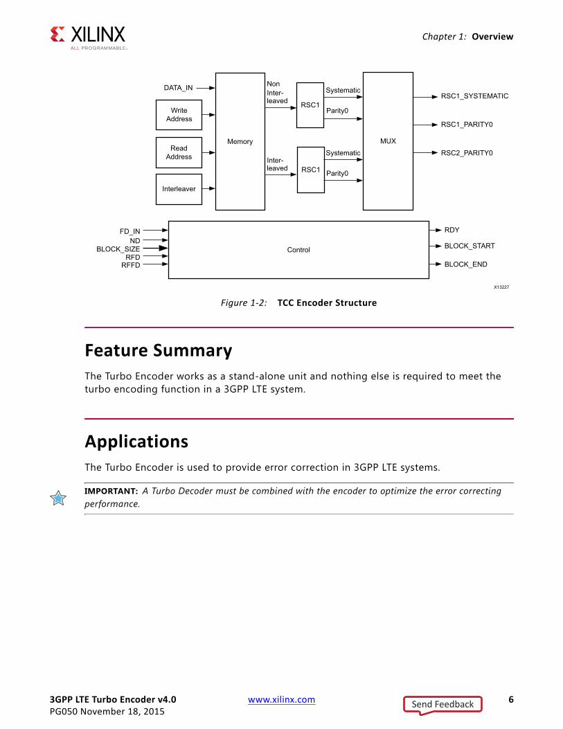
The 3GPP LTE Turbo Encoder input and output ports are shown in Figure 1-1, and the internal architecture is shown in Figure 1-2. It is a block-based processing unit where blocks between 40 bits and 6144 bits are input through the DATA_IN port and processed. Each block of data is processed in two identical Recursive Systematic Convolutional (RSC) encoders, which generate high-weight codes. RSC1 processes the raw input data, while RSC2 processes an interleaved version of the input data. The coding operates on the principle that if an input symbol is corrupted in the sequence from RSC1, then it is unlikely also to be corrupted in the interleaved sequence from RSC2, and vice versa.
Often some of the encoded output bits need not be transmitted, so they are omitted, or punctured from the output stream. Puncturing offers a dynamic trade-off between code rate and error performance. When the channel is noisy or the data requires more protection, extra redundancy can be added, thereby lowering the code rate. Puncturing is not implemented as part of the core.
X-Ref Target - Figure 1-1
Figure 1-1: TCC Encoder Pinout
3GPP LTE Turbo Encoder v4.0 www.xilinx.com 5PG050 November 18, 2015
Send Feedback
Chapter 1: Overview
Feature SummaryThe Turbo Encoder works as a stand-alone unit and nothing else is required to meet the turbo encoding function in a 3GPP LTE system.
ApplicationsThe Turbo Encoder is used to provide error correction in 3GPP LTE systems.
IMPORTANT: A Turbo Decoder must be combined with the encoder to optimize the error correcting performance.
X-Ref Target - Figure 1-2
Figure 1-2: TCC Encoder Structure
3GPP LTE Turbo Encoder v4.0 www.xilinx.com 6PG050 November 18, 2015
Send Feedback

Chapter 1: Overview
Licensing and Ordering InformationThis Xilinx® LogiCORE™ IP module is provided under the terms of the Xilinx Turbo Code LogiCORE IP License Terms. For full access to all core functionalities in simulation and in hardware, you must purchase a license for the core. Contact your local Xilinx sales representative for information about pricing and availability of Xilinx LogiCORE IP.
To evaluate this core in hardware, generate an evaluation license, which can be accessed from the Xilinx IP Evaluation page. After purchasing the core, you will receive instructions for registering and generating a full license. The full license can be requested and installed from the Xilinx IP Center for use with the Vivado® Design Suite.
For more information, visit the 3GPP LTE Turbo Encoder product web page.
Information about this and other Xilinx LogiCORE IP modules is available at the Xilinx Intellectual Property page. For information on pricing and availability of other Xilinx LogiCORE IP modules and tools, contact your local Xilinx sales representative.
France Telecom, for itself and certain other parties, claims certain intellectual property rights covering Turbo Codes technology, and has decided to license these rights under a licensing program called the Turbo Codes Licensing Program. Supply of this IP core does not convey a license nor imply any right to use any Turbo Codes patents owned by France Telecom, TDF or GET. Contact France Telecom for information about its Turbo Codes Licensing Program at the following address:
France Telecom R&DVAT/TURBOCODES38, rue du Général Leclerc92794 Issy MoulineauxCedex 9FRANCE.
3GPP LTE Turbo Encoder v4.0 www.xilinx.com 7PG050 November 18, 2015
Send Feedback

Chapter 2
Product Specification
Standards ComplianceThis version of the Turbo Convolution Code (TCC) Encoder is designed to meet the 3GPP TS 36.212 v9.0.0 Multiplexing and Channel Coding specification [Ref 1].
Performance
LatencyLatency is defined as the number of active clock cycles from the time the last bit of the f irst input block is accepted to the time at which RDY and BLOCK_START are asserted to indicate that the f irst block is ready to output. The latency value is defined only for the f irst block, because at other times the delay between a given block being input and that block being output depends on the number and size of blocks stored in the Data Memory.
ThroughputIn any 3GPP LTE Turbo Encoder, there must be a minimum of four idle clock cycles at the output due to the time required for the tail bits. In general, the maximum throughput for a given block size K is given by:
(K/(K+4)) x clock frequency (bits/s)
Example:
For a block size of 40 (worst case) and a clock rate of 250 MHz, the throughput is (40/(40+4))*250000000 or 227.3 Mb/s.
For a block size of 6144 (best case) and a clock rate of 250 MHz, the throughput is (6144/(6144+4))*250000000 or 249.8 Mb/s.
3GPP LTE Turbo Encoder v4.0 www.xilinx.com 8PG050 November 18, 2015
Send Feedback
Chapter 2: Product Specification
Resource UtilizationFor full details about performance and resource utilization, visit the Performance and Resource Utilization web page.
These results are obtained by double registering all input and output ports to reduce any dependency on I/O placement. The inner set of buffer registers operate at the core clock rate, whilst the outer operates at a different clock rate. This again helps to remove any effect of I/O placement on the core clock rate.
Core performance and resource requirements are provided as a guide only. Only the core and the double registers are placed into the FPGA to obtain these results so some variation in performance can be expected depending on how this core forms part of an overall system. The extra double registers are included in the resource count for this core.
Clock frequency does not take account of clock jitter and should therefore be derated by an amount appropriate to the clock source jitter specification.
3GPP LTE Turbo Encoder v4.0 www.xilinx.com 9PG050 November 18, 2015
Send Feedback

Chapter 2: Product Specification
Port DescriptionsThe I/O ports are summarized and described in Table 2-1.
Table 2-1: I/O Ports
Pin SensePort
Width(bits)
Description
CLK Input 1 Clock – All synchronous operations occur on the rising edge of the clock signal.
CE Input(optional) 1 Clock Enable – When deasserted (Low), rising clock edges
are ignored and the core is held in its current state.
SCLR Input(optional) 1 Synchronous Clear – When asserted (High) on an active
clock edge, the encoder is reset.
DATA_IN Input 1 Data Input – The data to be encoded.
BLOCK_SIZE Input 13 Block Size – The block size of the current encode operation.
ND Input(optional) 1 New Data – When ND is sampled High on a valid clock edge,
a new input value is read from the DATA_IN port.
FD_IN Input 1
First Data – FD_IN is asserted (High) on a valid clock edge to indicate that the f irst bit of a block is on the DATA_IN port and the BLOCK_SIZE port is sampled. FD_IN is qualif ied by ND.
RFD_IN Input(optional) 1
Ready For Data (Input) – A logic High on RFD_IN indicates that the downstream system is able to accept data from the core. The output side of the core is inhibited if RFD_IN is Low.
RSC1_SYSTEMATIC Output 1 RSC1_systematic – The systematic output from RSC1.
RSC1_PARITY0 Output 1 RSC1_parity0 – The parity0 output from RSC1.
RSC2_PARITY0 Output 1 RSC2_parity0 – The parity0 output from RSC2.
RFD Output 1 Ready For Data – When asserted (High), the core is ready to accept a new input bit on the DATA_IN port.
RFFD Output 1Ready For First Data – When asserted (High), the core is ready to accept a new input block. RFFD can be High only if RFD is High.
BLOCK_START Output 1Block Start – Indicates that the f irst data bit of an output block is on the systematic and parity outputs when asserted (High).
BLOCK_END Output 1 Block End – Indicates that the last tail bit of an output block is on the systematic and parity outputs when asserted (High).
RDY Output 1 Ready – Indicates that there is valid data on the systematic and parity outputs when asserted (High).
3GPP LTE Turbo Encoder v4.0 www.xilinx.com 10PG050 November 18, 2015
Send Feedback

Chapter 2: Product Specification
Clock (CLK)
All operations of the core are synchronized to the rising edge of CLK. If the optional CE pin is enabled, an active rising clock edge occurs only when CE is High. If CE is Low, the core is held in its current state.
Clock Enable (CE)
Clock enable is an optional input pin that is used to enable the synchronous operation of the core. When CE is High, a rising edge of CLK is acted upon by the core, but if CE is Low, the core remains in its current state. An active rising clock edge is one on which CE (if enabled) is sampled High. It should be noted that CE has a high fanout internal to the core, and this can result in a reduction in performance of about 10%.
Synchronous Clear (SCLR)
The SCLR signal is optional, and when it is asserted High on a valid clock edge, the core is reset to its initial state, that is, the core is ready to process a new block. Following the initial configuration of the FPGA, the core is automatically in the reset state, so no further SCLR is required before an encoding operation can take place. If the optional CE input port is selected, SCLR is ignored if CE is Low.
Data In (DATA_IN)
The DATA_IN port is a mandatory input port that carries the unencoded data. The input process is started with a valid-FD signal and data is read serially into the DATA_IN port on a clock-by-clock basis. Block size clock cycles are therefore required to input each block. DATA_IN can be qualif ied by the optional ND port. See New Data (ND).
New Data (ND)
The optional ND input port is used to indicate that there is new input data to be read from the DATA_IN port. For example, if the input block size is 40, then 40 active-High ND-samples are required to load a block of data into the encoder. ND should be asserted only when RFD is High. ND is also used to qualify the FD_IN input. See First Data (FD_IN).
First Data (FD_IN)
FD_IN is a mandatory input port used to start the encoder operation. FD_IN is qualif ied by the optional ND input. Furthermore, the core is sensitive to FD_IN only if the RFFD output is High. A valid-FD means that FD_IN and ND are both sampled High on an active rising clock edge when the RFFD output is High.
When a valid-FD occurs, the first data bit of a block is read from the DATA_IN port, and the block size is read from the BLOCK_SIZE port. The core then continues loading data, until a complete block has been input.
3GPP LTE Turbo Encoder v4.0 www.xilinx.com 11PG050 November 18, 2015
Send Feedback
Chapter 2: Product Specification
The FD_IN input should be asserted only when the RFFD output is High. See Ready For First Data (RFFD).
Block Size (BLOCK_SIZE)
This port determines the size of the block of data that is about to be written into the encoder. The block size value is sampled on an active rising clock edge when FD_IN is High and ND (if selected) is High. If an invalid block size (that is, not one of the 188 block sizes specified in 3GPP TS 36.212 v9.0.0 Multiplexing and Channel Coding specification [Ref 1] is sampled, the behavior of the core is not specif ied.
Ready For Data (RFD)
RFD is a mandatory output port that is asserted High when the core is ready to accept new data. If RFD is selected, then it is High during the period that a particular block is input. When block size samples of data have been input, the RFD signal goes Low to indicate that the core is no longer ready to accept data. The DATA_IN, BLOCK_SIZE, ND, and FD ports are sampled only if RFD is High.
Ready For First Data (RFFD)
RFFD is a mandatory output port that is asserted High when the core is ready to accept an FD_IN signal to start a new encoding operation. RFFD can be High only when RFD is also High. When a valid-FD signal is sampled, the RFFD output goes Low and remains Low until it is ready to accept another input block. The FD_IN and BLOCK_SIZE ports are sampled only if RFFD is High.
RSC1 Systematic Output (RSC1_SYSTEMATIC)
RSC1_SYSTEMATIC is a mandatory output port that is a delayed version of the uninterleaved input data. During trellis termination, the RSC1_SYSTEMATIC port also carries systematic and parity tail bits.
RSC1 Parity0 Output (RSC1_PARITY0)
RSC1_PARITY0 is a mandatory output port that is the Y0 output from RSC1 (see Figure 1-2). During trellis termination, the RSC1_PARITY0 port also carries systematic and parity tail bits.
RSC2 Parity0 Output (RSC2_PARITY0)
RSC2_PARITY0 is a mandatory output port that is the Y0 output from RSC2 (see Figure 1-2). During trellis termination, the RSC2_PARITY0 port also carries systematic and parity tail bits.
3GPP LTE Turbo Encoder v4.0 www.xilinx.com 12PG050 November 18, 2015
Send Feedback

Chapter 2: Product Specification
Block Start (BLOCK_START)
This signal is asserted High for one clock cycle when the first valid data bit of a block is on the systematic and parity output ports.
Block End (BLOCK_END)
This signal is asserted High for one clock cycle when the last tail bit of a block is on the systematic and parity output ports.
Ready (RDY)
This signal is asserted High when there is valid data on the systematic and parity output ports, including the tail bits. RDY is asserted for block size plus four clock cycles for every encoded block. If the core is running at maximum throughput, RDY does not go Low between blocks. For this reason, it is recommended to use the BLOCK_START output to indicate the start of an output block.
Ready For Data In (RFD_IN)
RFD_IN is an optional pin that can be used to inhibit the output side of the core while allowing current input operations to continue. RFD_IN is intended to be used as a means for a downstream system using the encoded data to indicate that it is not ready to handle any further data. If RFD_IN is Low, all systematic and parity outputs, BLOCK_START, BLOCK_END, and RDY outputs are inhibited. The operation of RFD_IN is described in further detail later in this document.
3GPP LTE Turbo Encoder v4.0 www.xilinx.com 13PG050 November 18, 2015
Send Feedback
Chapter 3
Designing with the CoreThis chapter includes guidelines and additional information to facilitate designing with the core.
General Design Guidelines
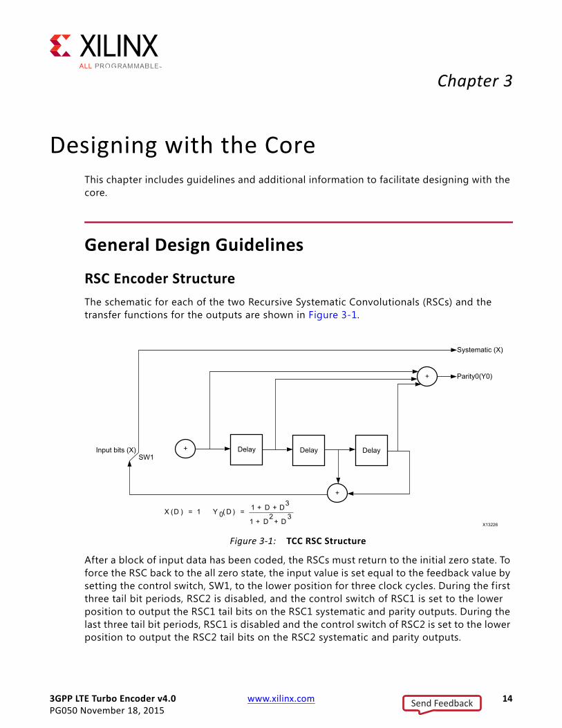
RSC Encoder StructureThe schematic for each of the two Recursive Systematic Convolutionals (RSCs) and the transfer functions for the outputs are shown in Figure 3-1.
After a block of input data has been coded, the RSCs must return to the initial zero state. To force the RSC back to the all zero state, the input value is set equal to the feedback value by setting the control switch, SW1, to the lower position for three clock cycles. During the first three tail bit periods, RSC2 is disabled, and the control switch of RSC1 is set to the lower position to output the RSC1 tail bits on the RSC1 systematic and parity outputs. During the last three tail bit periods, RSC1 is disabled and the control switch of RSC2 is set to the lower position to output the RSC2 tail bits on the RSC2 systematic and parity outputs.
X-Ref Target - Figure 3-1
Figure 3-1: TCC RSC Structure
3GPP LTE Turbo Encoder v4.0 www.xilinx.com 14PG050 November 18, 2015
Send Feedback

Chapter 3: Designing with the Core
In practice, the 12 tail bit values from RSC1_systematic, RSC2_systematic, RSC1_Parity0, and RSC2_Parity0 are re-multiplexed onto RSC1_systematic, RSC1_Parity0, and RSC2_Party0 outputs over four clock cycles. See Trellis Termination.
ClockingSee Clock (CLK).
ResetsSee Synchronous Clear (SCLR).
Functional Description
FIFO BufferingFigure 3-2 illustrates the process by which the core buffers incoming blocks in First-In-First-Out (FIFO) order. Input data bits are written in linear order into the Data Memory at contiguous addresses. Each time a complete input block has been written into the Data Memory, its block size is written to the Block Size FIFO.
When the core is ready to output a block, the block size is read from the Block Size FIFO. This determines the block size parameter for the interleaved and non-interleaved read address generators and is also utilized to calculate the base address for the next block.
As the Data Memory is dual-ported, the write and read operations are independent; this allows maximum throughput to be achieved for any arbitrary sequence of block sizes.
In addition, by using the optional ND and RFD_IN ports, the input and output processes can be independently flow-controlled while still maintaining maximum throughput.
If either the Data Memory or the Block Size FIFO becomes full, the core deasserts RFD to prevent any more data being written. If the Block Size FIFO becomes empty, the core deasserts RDY to indicate that there is no data to output. These processes are described in more detail later in this data sheet.
3GPP LTE Turbo Encoder v4.0 www.xilinx.com 15PG050 November 18, 2015
Send Feedback

Chapter 3: Designing with the Core
Data MemoryThe data memory consists of two 16384 x 1 dual-port memories. Data bits are written in linear order into both dual-port memories at the same modulo-16384 addresses. One of the memories is read in non-interleaved order, to provide data for RSC1, while the other is read in interleaved order to provide data for RSC2.
The data memory can accommodate two of the largest 3GPP LTE blocks, that is, 6144 bits. This ensures that maximum throughput can be obtained with a continuous stream of the largest block size.
If the data memory becomes full, the core deasserts the RFD output port to indicate that the core can accept no more data. More precisely, RFD is deasserted if the acceptance of the next input bit would cause the f irst bit of an unread data block in the data memory to be overwritten. RFD is asserted again when that data block has been completely output.
Block Size FIFOThe Block Size FIFO can be implemented in SRL32 or block RAM, as selected by the Block Capacity menu in the Vivado® IP catalog GUI.
Possible values for Block Capacity are 32 or Max.
• Block Capacity value Max selects a 512-deep block RAM FIFO, but reflects that the maximum possible number of 40-bit blocks that can be held in 16K of RAM is 409.
• When the Block Capacity value is 32, it is possible for Block Size FIFO to become full.
If the Block Size FIFO becomes full, the core drives RFD Low to inhibit the input until space becomes available in the FIFO, due to the output side of the core fetching a block size from the FIFO.
If the Block Size FIFO becomes empty, then, when the core has output the last bit of the current output block, it deasserts RDY to indicate that there is no data to output.
X-Ref Target - Figure 3-2
Figure 3-2: FIFO Buffering
3GPP LTE Turbo Encoder v4.0 www.xilinx.com 16PG050 November 18, 2015
Send Feedback

Chapter 3: Designing with the Core
Input Control SignalsFigure 3-3a shows the signals associated with the data input side of the core. If, on an active rising edge of CLK, FD_IN and ND (if selected) are both sampled High, this is known as a valid-FD, or valid First Data signal.
When a valid-FD is sampled, the RFFD signal is driven Low to indicate that the core is no longer waiting for FD_IN. The block size, in this case n, of the current input block is sampled on the BLOCK_SIZE port, and the first data symbol, d1, is sampled on the DATA_IN port.
A High on the ND port indicates that the value on the DATA_IN port is new data. If ND is sampled Low, then the DATA_IN port is not sampled, and the internal write address does not advance.
The core continues to input data, until n new data samples have been accepted, whereupon RFFD is normally driven High to indicate that the core is ready for a new input block.
After asserting RFFD, the core waits until the next valid-FD is sampled, whereupon a new write cycle is started, in this case with block size N.
The behavior of the core is not specified if, on a valid-FD, an invalid block size is sampled. If this condition occurs, the core should be reset by asserting SCLR.
Trellis TerminationAs specified in 3GPP TS 36.212 v9.0.0 Multiplexing and Channel Coding specification [Ref 1], the 12 trellis termination bits of RSC1 and RSC2 (see Figure 3-1) are re-multiplexed, over four clock cycles, onto the RSC1_SYSTEMATIC, RSC1_PARITY0, and RSC2_PARITY0 output ports. These bits are then transmitted in the following sequence:
xn+1, zn+1, xn+2, zn+2, xn+3, zn+3, x’n+1, z’n+1, x’n+2, z’n+2, x’n+3 ,z’n+3.
Output Control SignalsThe RDY port is driven High to indicate that there is valid data on the systematic and parity ports. When the f irst valid data bit is on the output ports, the BLOCK_START output is driven High, and when the last tail bit is on the output ports, the BLOCK_END output is driven High. The output timing is shown in Figure 3-3b.
3GPP LTE Turbo Encoder v4.0 www.xilinx.com 17PG050 November 18, 2015
Send Feedback

Chapter 3: Designing with the Core
X-Ref Target - Figure 3-3
Figure 3-3: Input and Output Timing
x1 ..
. xn
are
the
unin
terle
aved
inpu
t bits
, del
ayed
, for
blo
ck s
ize
nx’
1 ...
x’n
are
the
inte
rleav
ed in
put b
itsz1
... z
n+3
are
the
RSC1
Par
ity0
outp
ut b
itsz’
1 ...
z’n
+3
are
the
RSC2
Par
ity0
outp
ut b
its
a. In
put T
imin
g
b. O
utpu
t Tim
ing
3GPP LTE Turbo Encoder v4.0 www.xilinx.com 18PG050 November 18, 2015
Send Feedback
Chapter 3: Designing with the Core
Flow control on the output side can be implemented with the optional RFD_IN input port. If the RFD_IN port is sampled Low on an active rising clock edge, the RSC output ports, RDY, and the internal circuitry associated with these outputs are frozen.
The latency delay is affected by the optional RFD_IN input. The RFD_IN input should be driven Low only to inhibit the core output when RDY is High.
The input side of the core is not directly affected by the RFD_IN port. However, if RFD_IN is deasserted often enough, the time taken to output blocks can be extended, such that either the Data Memory or the Block Size FIFO can become full, whereupon the core deasserts RFD to indicate that it cannot accept any more input bits.
3GPP LTE Turbo Encoder v4.0 www.xilinx.com 19PG050 November 18, 2015
Send Feedback

Chapter 4
Design Flow StepsThis chapter describes customizing and generating the core, constraining the core, and the simulation, synthesis and implementation steps that are specific to this IP core. More detailed information about the standard Vivado® design flows and the IP integrator can be found in the following Vivado Design Suite user guides:
• Vivado Design Suite User Guide: Designing IP Subsystems using IP Integrator (UG994) [Ref 3]
• Vivado Design Suite User Guide: Designing with IP (UG896) [Ref 5]
• Vivado Design Suite User Guide: Getting Started (UG910) [Ref 6]
• Vivado Design Suite User Guide: Logic Simulation (UG900) [Ref 7]
Customizing and Generating the CoreThis section includes information about using Xilinx® tools to customize and generate the core in the Vivado Design Suite.
If you are customizing and generating the core in the Vivado IP Integrator, see the Vivado Design Suite User Guide: Designing IP Subsystems using IP Integrator (UG994) [Ref 3] for detailed information. IP Integrator might auto-compute certain configuration values when validating or generating the design. To check whether the values do change, see the description of the parameter in this chapter. To view the parameter value you can run the validate_bd_design command in the tcl console.
You can customize the IP for use in your design by specifying values for the various parameters associated with the IP core using the following steps:
1. Select the IP from the IP catalog.
2. Double-click the selected IP or select the Customize IP command from the toolbar or right-click menu.
For details, see the Vivado Design Suite User Guide: Designing with IP (UG896) [Ref 5] and the Vivado Design Suite User Guide: Getting Started (UG910) [Ref 6].
3GPP LTE Turbo Encoder v4.0 www.xilinx.com 20PG050 November 18, 2015
Send Feedback

Chapter 4: Design Flow Steps
Accessing and Configuring the Core
To access and configure the 3GPP LTE Turbo Encoder:
1. Open an existing project or create a new project in the Vivado Design Suite.
2. Open the IP catalog and navigate to 3GPP LTE Turbo Encoder.
3. Double-click the core to open the Customize IP dialog box for 3GPP LTE Turbo Encoder.
4. In the Customize IP dialog box, select the pins for the core.
5. Select the size of the Block Size FIFO as described in the Block Size FIFO in Chapter 3.
° Select Max to use a block RAM. Selecting Max is the recommended approach if more than 32 blocks can be stored within the core at any time.
° Select 32 to use distributed RAM for the FIFO. A value of 32 can be used to remove the requirement of the BRAM.
User ParametersTable 4-1 shows the relationship between the GUI f ields in the Vivado IDE and the User Parameters (which can be viewed in the Tcl console). All parameters are available in the IP integrator and none are set automatically.
Output GenerationFor details, see the Vivado Design Suite User Guide: Designing with IP (UG896) [Ref 5].
Table 4-1: GUI Parameter to User Parameter Relationship
GUI Parameter/Value(1) User Parameter/Value(1) Default Value
ND nd false
RFD IN rfd_in False
CE ce False
SCLR sclr False
Block Capacity block_capacity 32
32 32
Max 512
Notes: 1. Parameter values are listed in the table where the GUI parameter value differs from the user parameter value. Such
values are shown in this table as indented below the associated parameter.
3GPP LTE Turbo Encoder v4.0 www.xilinx.com 21PG050 November 18, 2015
Send Feedback
Chapter 4: Design Flow Steps
Constraining the CoreThis section contains information about constraining the core in the Vivado Design Suite.
Required ConstraintsThis section is not applicable for this IP core.
Device, Package, and Speed Grade SelectionsThis section is not applicable for this IP core.
Clock FrequenciesThis section is not applicable for this IP core.
Clock ManagementThis section is not applicable for this IP core.
Clock PlacementThis section is not applicable for this IP core.
BankingThis section is not applicable for this IP core.
Transceiver PlacementThis section is not applicable for this IP core.
I/O Standard and PlacementThis section is not applicable for this IP core.
SimulationFor comprehensive information about Vivado simulation components, as well as information about using supported third party tools, see the Vivado Design Suite User Guide: Logic Simulation (UG900) [Ref 7].
3GPP LTE Turbo Encoder v4.0 www.xilinx.com 22PG050 November 18, 2015
Send Feedback
Chapter 4: Design Flow Steps
Synthesis and ImplementationFor details about synthesis and implementation, see “Synthesizing IP” and “Implementing IP” in the Vivado Design Suite User Guide: Designing with IP (UG896) [Ref 5].
3GPP LTE Turbo Encoder v4.0 www.xilinx.com 23PG050 November 18, 2015
Send Feedback
Chapter 5
C Model ReferenceThe Xilinx® LogiCORE™ IP 3GPP LTE Turbo Encoder core has a bit accurate C model designed for system modeling. This allows you to model the core performance. For purposes of abbreviation, 3GPP LTE Turbo Encoder is used interchangeably with LTE-TCC throughout this section. The C model for the 3GPP LTE Turbo Encoder is available with the core in the Vivado® Design Suite.
Features• Bit accurate to 3GPP LTE Turbo Encoder core
• Available for 32-bit and 64-bit Linux platforms
• Available for 32-bit and 64-bit Windows platforms
• Designed for integration into a larger system model
• Example C++ code provided showing how to use the C model functions
The model consists of a set of C functions that reside in a shared library. Example C code is provided to demonstrate how these functions form the interface to the C model. Full details of this interface are given in 3GPP LTE Turbo Encoder C Model Interface.
The model is bit accurate but not cycle-accurate, so it produces exactly the same output data as the core on a block-by-block basis. However, it does not model the core latency or its interface signals.
3GPP LTE Turbo Encoder v4.0 www.xilinx.com 24PG050 November 18, 2015
Send Feedback

Chapter 5: C Model Reference
User Instructions
Unpacking and Model ContentsThe C model is supplied as a platform specific zip f ile, tcc_encoder_3gpplte_v4_0_bitacc_cmodel_*.zip, where * is lin, lin64, nt or nt64, depending on the target platform of the contained libraries.
• For Linux platforms, a shared object library, libIp_tcc_encoder_3gpplte_v4_0_bitacc_model.so, contains the model.
• For Windows platforms, a dynamically linked library, libIp_tcc_encoder_3gpplte_v4_0_bitacc_cmodel.dll, contains the model. Also included is a .lib f ile for compiling.
The files that are provided across all platforms are detailed in Table 5-1.
InstallationOn Linux, ensure that the directory in which the f ile libIp_tcc_encoder_3gpplte_v4_0_bitacc_cmodel.so is located is on your $LD_LIBRARY_PATH environment variable, or is the directory in which you run your executable that calls the LTE-TCC C model.
On Windows, ensure that the directory in which the file libIp_tcc_encoder_3gpplte_v4_0_bitacc_cmodel.dll is located is either on your $PATH environment variable, or is the directory in which you run your executable that calls the LTE-TCC C model.
Table 5-1: C Model Directory Structure and Files
File Description
tcc_encoder_3gpplte_v4_0_bitacc_cmodel.h Model header file
run_bitacc_cmodel.c Example code calling the model
3GPP LTE Turbo Encoder v4.0 www.xilinx.com 25PG050 November 18, 2015
Send Feedback
Chapter 5: C Model Reference
3GPP LTE Turbo Encoder C Model Interface The Application Programming Interface (API) of the C model is defined in the header f ile tcc_encoder_3gpplte_v4_0_bitacc_cmodel.h. The interface consists of four functions, and four structures supporting those functions.
StructuresThe interface consists of the following structures.
Generics
The xilinx_ip_tcc_encoder_3gpplte_v4_0_generics structure specifies the generics that should apply to the modeled core. The structure contains fields for the core generics; however currently none of these generics affect the bit accuracy of the model. The generics are detailed in Table 5-2.
State
The xilinx_ip_tcc_encoder_3gpplte_v4_0_state structure defines the internal state of the C model. Because the structure is solely for internal use by the C model, the layout of the structure is not defined. User modification of the state structure can lead to undefined behavior.
Input
The xilinx_ip_tcc_encoder_3gpplte_v4_0_inputs structure is used to specify input data for the C model. See Table 5-3.
Table 5-2: Generics Structure
Member Type Description
C_FAMILY char* Device family.
C_ELABORATION_DIR char* Core elaboration directory.
C_HAS_RFD_IN int Output flow control port present.
C_HAS_CE int Clock enable port present.
C_HAS_ND int Input flow control port present.
C_HAS_SCLR int Synchronous clear port present.
C_MAX_BLOCKS int Maximum block storage capacity (32, 512)
3GPP LTE Turbo Encoder v4.0 www.xilinx.com 26PG050 November 18, 2015
Send Feedback
Chapter 5: C Model Reference
The din array is used to pass the bit inputs into the C model. The din_size f ield defines the size of the din array and should be equal to the code block size.
Allocation of the arrays is your responsibility. They can be allocated statically or dynamically. If allocated dynamically, you are responsible for de-allocation. The arrays might be larger than that specified by din_size, allowing the arrays to be pre-allocated for the largest code block (6144 bits). The C model uses only the f irst din_size elements of each array.
Output
The xilinx_ip_tcc_encoder_3gpplte_v4_0_outputs structure is used to specify output data from the C model. See Table 5-4.
The rsc1_sys, rsc1_par and rsc2_par arrays are used to receive encoded data from the C model. After a successful encode, each element of each array holds a single encoded data bit. The arrays also contain tail bits. The 12 tail bits are distributed across the three arrays, four extra bits per array, as described in RSC Encoder Structure.
Allocation of the arrays is your responsibility. They can be allocated statically or dynamically. If allocated dynamically, then you are responsible for de-allocation. The max_dout_size f ield is used to specify the size of the allocated arrays. When encoding a code block, the C model checks that the output arrays have suff icient space for the encoded data before updating the dout_size f ield with the actual code block size, plus four bits to account for the tail bits.
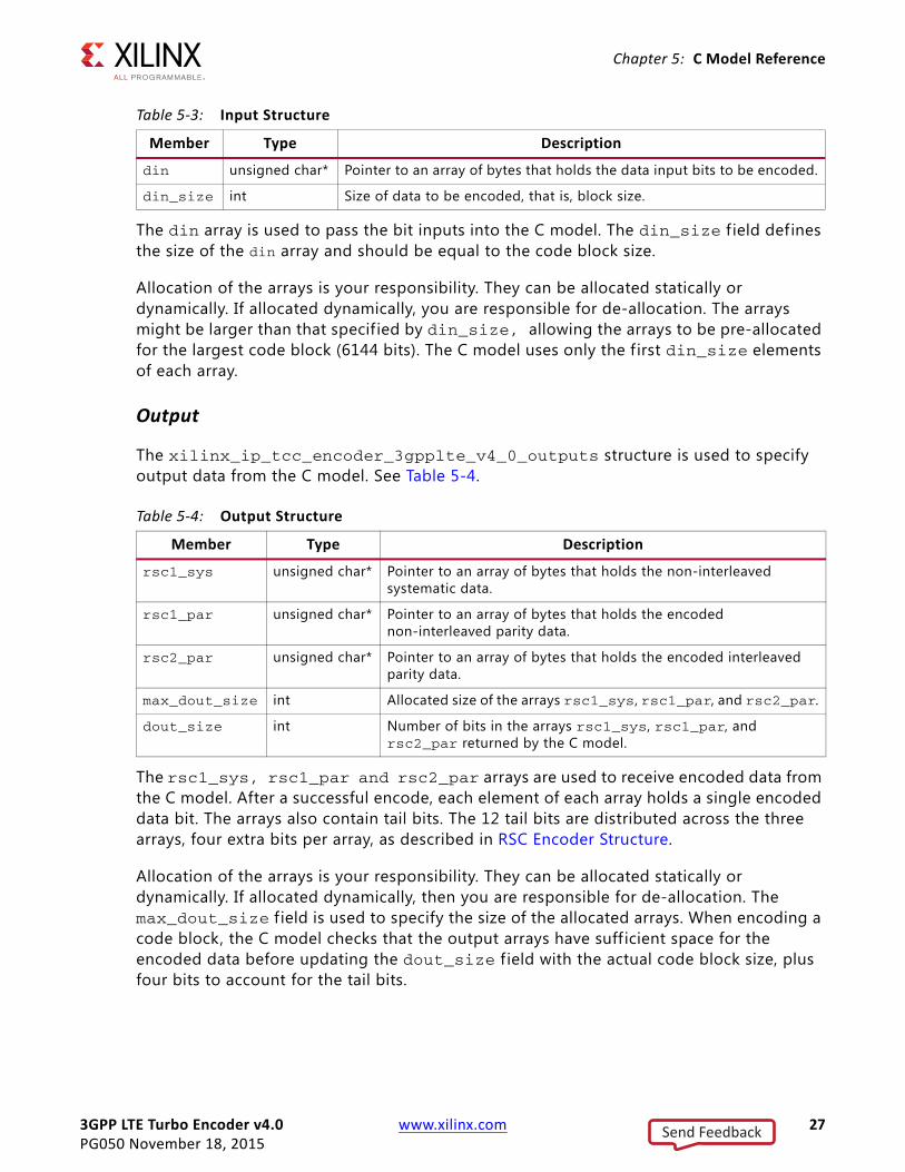
Table 5-3: Input Structure
Member Type Description
din unsigned char* Pointer to an array of bytes that holds the data input bits to be encoded.
din_size int Size of data to be encoded, that is, block size.
Table 5-4: Output Structure
Member Type Description
rsc1_sys unsigned char* Pointer to an array of bytes that holds the non-interleaved systematic data.
rsc1_par unsigned char* Pointer to an array of bytes that holds the encoded non-interleaved parity data.
rsc2_par unsigned char* Pointer to an array of bytes that holds the encoded interleaved parity data.
max_dout_size int Allocated size of the arrays rsc1_sys, rsc1_par, and rsc2_par.
dout_size int Number of bits in the arrays rsc1_sys, rsc1_par, and rsc2_par returned by the C model.
3GPP LTE Turbo Encoder v4.0 www.xilinx.com 27PG050 November 18, 2015
Send Feedback
Chapter 5: C Model Reference
FunctionsThe interface consists of the following functions.
Default Generics
The xilinx_ip_tcc_encoder_3gpplte_v4_0_get_default_generics function is used to create a default xilinx_ip_tcc_encoder_3gpplte_v4_0_generics structure:
struct xilinx_ip_tcc_encoder_3gpplte_v4_0_generics xilinx_ip_tcc_encoder_3gpplte_v4_0_get_default_generics();
The function returns a default generic structure which can be used directly, as further customization has no effect on the operation of the model.
Create State
The xilinx_ip_tcc_encoder_3gpplte_v4_0_create_state function creates a new state structure based on the given generics:
struct xilinx_ip_tcc_encoder_3gpplte_v4_0_state* xilinx_ip_tcc_encoder_3gpplte_v4_0_create_state( struct xilinx_ip_tcc_encoder_3gpplte_v4_0_generics generics);
The function returns a pointer to the created state structure. If the state structure cannot be created, then an error message is produced on standard error and the function returns a null pointer.
Simulate
The xilinx_ip_tcc_encoder_3gpplte_v4_0_bitacc_simulate function encodes a single code block:
int xilinx_ip_tcc_encoder_3gpplte_v4_0_bitacc_simulate( struct xilinx_ip_tcc_encoder_3gpplte_v4_0_state* state, struct xilinx_ip_tcc_encoder_3gpplte_v4_0_inputs inputs, struct xilinx_ip_tcc_encoder_3gpplte_v4_0_outputs* outputs);
On entry, you must initialize all f ields of the inputs structure. The din array should be f illed with input data. Additionally, the rsc1_sys, rsc1_par, rsc2_par and max_dout_size f ields of the outputs structure must be initialized to indicate to the C model the location and size of the output arrays. The dout_size f ield of the outputs structure is set by the function on exit.
3GPP LTE Turbo Encoder v4.0 www.xilinx.com 28PG050 November 18, 2015
Send Feedback
Chapter 5: C Model Reference
The function returns zero if the code block was successfully encoded. If the code block could not be encoded, an error message is produced on standard error and the function returns a non-zero error code.
Destroy State
The xilinx_ip_tcc_encoder_3gpplte_v4_0_destroy_state function destroys a state structure:
void xilinx_ip_tcc_encoder_3gpplte_v4_0_destroy_state( struct xilinx_ip_tcc_encoder_3gpplte_v4_0_state* state);
On return, any memory resources allocated within the state structure are released and the state structure becomes undefined.
CompilingCompilation of user code requires access to the tcc_encoder_3gpplte_v4_0_bitacc_cmodel.h header file. The header f ile should be copied to a location where it is available to the compiler. Depending on the location chosen, the include search path of the compiler might need to be modif ied.
LinkingTo use the C model, the user executable must be linked against the correct libraries for the target platform.
Linux
The executable must be linked against the libIp_tcc_encoder_3gpplte_v4_0_bitacc_cmodel.so shared object library. Files for 32-bit and 64-bit systems are supplied in the lin and lin64 directories, respectively.
Using GCC, linking is typically achieved by adding the following command line options:
-L. -lIp_tcc_encoder_3gpplte_v4_0_bitacc_cmodel
This assumes the three shared object libraries are in the current directory. If this is not the case, the –L. option should be changed to specify the library search path to use.
Using GCC, the provided example program run_bitacc_cmodel.c can be compiled and linked using the following command:
gcc -x c++ -I. -L. -lIp_tcc_encoder_3gpplte_v4_0_bitacc_cmodel run_bitacc_cmodel.c -o run_bitacc_cmodel
3GPP LTE Turbo Encoder v4.0 www.xilinx.com 29PG050 November 18, 2015
Send Feedback

Chapter 5: C Model Reference
Windows
The executable must be linked against the libIp_tcc_encoder_3gpplte_v4_0_bitacc_cmodel.dll dynamic link library. Depending on the compiler, the import library libIp_tcc_encoder_3gpplte_v4_0_bitacc_cmodel.lib might be required. Files for 32-bit and 64-bit systems are supplied in the nt and nt64 directories, respectively.
ExampleThe run_bitacc_cmodel.c f ile contains example code to show basic operation of the C model.
3GPP LTE Turbo Encoder v4.0 www.xilinx.com 30PG050 November 18, 2015
Send Feedback

3GPP LTE Turbo Encoder v4.0 www.xilinx.com 31PG050 November 18, 2015
Appendix A
Migrating and UpgradingThis appendix contains information about upgrading to a more recent version of the IP core.
Migrating to the Vivado Design SuiteFor information about migrating to the Vivado Design Suite, see the ISE to Vivado Design Suite Migration Guide (UG911) [Ref 8].
Upgrading in the Vivado Design SuiteThis section provides information about any changes to the user logic or port designations that take place when you upgrade to a more current version of this IP core in the Vivado Design Suite.
Parameter ChangesNo change.
Port ChangesNo change.
Other ChangesNo change.
Send Feedback

Appendix B
DebuggingThis appendix includes details about resources available on the Xilinx® Support website and debugging tools.
Finding Help on Xilinx.comTo help in the design and debug process when using the 3GPP LTE Turbo Encoder, the Xilinx Support web page contains key resources such as product documentation, release notes, answer records, information about known issues, and links for obtaining further product support.
DocumentationThis product guide is the main document associated with the 3GPP LTE Turbo Encoder. This guide, along with documentation related to all products that aid in the design process, can be found on the Xilinx Support web page or by using the Xilinx Documentation Navigator.
Download the Xilinx Documentation Navigator from the Downloads page. For more information about this tool and the features available, open the online help after installation.
Solution CentersSee the Xilinx Solution Centers for support on devices, software tools, and intellectual property at all stages of the design cycle. Topics include design assistance, advisories, and troubleshooting tips.
Answer RecordsAnswer Records include information about commonly encountered problems, helpful information on how to resolve these problems, and any known issues with a Xilinx product. Answer Records are created and maintained daily ensuring that you have access to the most accurate information available.
3GPP LTE Turbo Encoder v4.0 www.xilinx.com 32PG050 November 18, 2015
Send Feedback
Appendix B: Debugging
Answer Records for this core are listed below, and can be located by using the Search Support box on the main Xilinx support web page. To maximize your search results, use proper keywords such as
• Product name
• Tool messages
• Summary of the issue encountered
A filter search is available after results are returned to further target the results.
Answer Records for the 3GPP LTE Turbo Encoder
AR: 54470
Technical SupportXilinx provides technical support in the Xilinx Support web page for this LogiCORE™ IP product when used as described in the product documentation. Xilinx cannot guarantee timing, functionality, or support if you do any of the following:
• Implement the solution in devices that are not defined in the documentation.
• Customize the solution beyond that allowed in the product documentation.
• Change any section of the design labeled DO NOT MODIFY.
To contact Xilinx Technical Support, navigate to the Xilinx Support web page.
3GPP LTE Turbo Encoder v4.0 www.xilinx.com 33PG050 November 18, 2015
Send Feedback
Appendix B: Debugging
Debug ToolsThere are many tools available to address 3GPP LTE Turbo Encoder design issues. It is important to know which tools are useful for debugging various situations.
Vivado Design Suite Debug FeatureThe Vivado® Design Suite debug feature inserts logic analyzer and virtual I/O cores directly into your design. The debug feature also allows you to set trigger conditions to capture application and integrated block port signals in hardware. Captured signals can then be analyzed. This feature in the Vivado IDE is used for logic debugging and validation of a design running in Xilinx devices.
The Vivado logic analyzer is used with the logic debug IP cores, including:
• ILA 2.0 (and later versions)
• VIO 2.0 (and later versions)
See Vivado Design Suite User Guide: Programming and Debugging (UG908) [Ref 9].
C Model ReferenceSee Chapter 5, C Model Reference in this guide for tips and instructions for using the provided C Model f iles to debug your design.
3GPP LTE Turbo Encoder v4.0 www.xilinx.com 34PG050 November 18, 2015
Send Feedback

Appendix C
Additional Resources and Legal Notices
Xilinx ResourcesFor support resources such as Answers, Documentation, Downloads, and Forums, see Xilinx Support.
ReferencesThese documents provide supplemental material useful with this guide:
1. 3GPP TS 36.212 V9.0.0 (2009-12) 3rd Generation Partnership Project; Technical Specification Group Radio Access Network; Multiplexing and Channel Coding (Release 9).
2. Near Shannon Limit Error-correcting Coding and Decoding Turbo Codes, C. Berrou, A. Glavieux, and P. Thitimajshima, IEEE Proc 1993, Int. Conf. Comm., pp1064-1070.
3. Vivado Design Suite User Guide: Designing IP Subsystems using IP Integrator (UG994)
4. Vivado Design Suite User Guide: Implementation (UG904)
5. Vivado Design Suite User Guide: Designing with IP (UG896)
6. Vivado Design Suite User Guide: Getting Started (UG910)
7. Vivado Design Suite User Guide - Logic Simulation (UG900)
8. ISE® to ISE to Vivado Design Suite Migration Guide (UG911)
9. Vivado Design Suite User Guide: Programming and Debugging (UG908)
3GPP LTE Turbo Encoder v4.0 www.xilinx.com 35PG050 November 18, 2015
Send Feedback

Appendix C: Additional Resources and Legal Notices
Revision HistoryThe following table shows the revision history for this document.
Please Read: Important Legal NoticesThe information disclosed to you hereunder (the "Materials") is provided solely for the selection and use of Xilinx products. To the maximum extent permitted by applicable law: (1) Materials are made available "AS IS" and with all faults, Xilinx hereby DISCLAIMS ALL WARRANTIES AND CONDITIONS, EXPRESS, IMPLIED, OR STATUTORY, INCLUDING BUT NOT LIMITED TO WARRANTIES OF MERCHANTABILITY, NON-INFRINGEMENT, OR FITNESS FOR ANY PARTICULAR PURPOSE; and (2) Xilinx shall not be liable (whether in contract or tort, including negligence, or under any other theory of liability) for any loss or damage of any kind or nature related to, arising under, or in connection with, the Materials (including your use of the Materials), including for any direct, indirect, special, incidental, or consequential loss or damage (including loss of data, profits, goodwill, or any type of loss or damage suffered as a result of any action brought by a third party) even if such damage or loss was reasonably foreseeable or Xilinx had been advised of the possibility of the same. Xilinx assumes no obligation to correct any errors contained in the Materials or to notify you of updates to the Materials or to product specifications. You may not reproduce, modify, distribute, or publicly display the Materials without prior written consent. Certain products are subject to the terms and conditions of Xilinx's limited warranty, please refer to Xilinx's Terms of Sale which can be viewed at http://www.xilinx.com/legal.htm#tos; IP cores may be subject to warranty and support terms contained in a license issued to you by Xilinx. Xilinx products are not designed or intended to be fail-safe or for use in any application requiring fail-safe performance; you assume sole risk and liability for use of Xilinx products in such critical applications, please refer to Xilinx's Terms of Sale which can be viewed at http://www.xilinx.com/legal.htm#tos.© Copyright 2012–2015 Xilinx, Inc. Xilinx, the Xilinx logo, Artix, ISE, Kintex, Spartan, Virtex, Vivado, Zynq, and other designated brands included herein are trademarks of Xilinx in the United States and other countries. AMBA, AMBA Designer, ARM, ARM1176JZ-S, CoreSight, Cortex, and PrimeCell are trademarks of ARM in the EU and other countries. All other trademarks are the property of their respective owners.
Date Version Revision
11/18/2015 4.0 • Added support for UltraScale+ families.• Updated link to resource utilization f igures.
04/02/2014 4.0 • Added link to resource utilization figures• Updated Template
12/18/2013 4.0 • Added UltraScale™ architecture support
10/02/2013 4.0 • Revision number advanced to 4.0 to align with core version number 4.0• C Model updates
03/20/2013 2.0 • Updated for core v4.0 and for Vivado Design Suite-only support• Major revisions to Chapter 4, Customizing and Generating the Core and
Appendix B, Debugging• Updated date and description in revision entry above
07/25/2012 1.0 First Xilinx release as a product guide. This document is derived from DS701 and UG506 for Vivado Design Suite 2012.2.
3GPP LTE Turbo Encoder v4.0 www.xilinx.com 36PG050 November 18, 2015
Send Feedback


