29
W74M64FV Publication Release Date: November 18, 2016 - 0 - Preliminary - Revision B 3V 64M-BIT SERIAL FLASH MEMORY WITH DUAL/QUAD SPI & SECURE AUTHENTICATION
W74M64FV
Publication Release Date: November 18, 2016
- 0 - Preliminary - Revision B
3V 64M-BIT
SERIAL FLASH MEMORY WITH
DUAL/QUAD SPI & SECURE AUTHENTICATION
W74M64FV
- 1 -
Table of Contents
GENERAL DESCRIPTIONS ............................................................................................................. 3
FEATURES ....................................................................................................................................... 3
PACKAGE TYPES AND PIN CONFIGURATIONS .......................................................................... 4
Pin Configuration SOIC 208-mil ........................................................................................... 4
Pin Description SOIC 208-mil ............................................................................................... 4
PIN DESCRIPTIONS ........................................................................................................................ 5
Chip Select (/CS) .................................................................................................................. 5
Serial Data Input, Output and IOs (DI, DO and IO0, IO1, IO2, IO3) .................................... 5
Serial Clock (CLK) ................................................................................................................ 5
BLOCK DIAGRAMS.......................................................................................................................... 6
Operation Diagram ............................................................................................................... 6
Functional Block Diagram .................................................................................................... 6
FUNCTIONAL DESCRIPTIONS ....................................................................................................... 7
Authentication Flash Operations .......................................................................................... 7
6.1.1 Authentication Flash Initialization ............................................................................................ 7
6.1.2 Authentication Flash Operation Flow ...................................................................................... 8
6.1.3 Operations Allowed / Disallowed to Authentication Flash ....................................................... 9
6.1.4 Authentication Flash Status Register Definition .................................................................... 10
Instruction Set Tables ......................................................................................................... 11
6.2.1 Instruction Set Table 2-1 (Authentication Flash Input Instruction, OP1)(1) ............................. 11
6.2.2 Instruction Set Table 2-2 (Authentication Flash Output Instruction, OP2)(1) .......................... 11
6.2.3 Instruction Set Table 2-3 (Authentication Flash Reset Instruction)(1) .................................... 11
Instruction Descriptions ...................................................................................................... 12
6.3.1 Write Root Key Register (9Bh + 00h) .................................................................................... 12
6.3.2 Update HMAC Key (9Bh + 01h) ............................................................................................ 13
6.3.3 Increment Monotonic Counter (9Bh + 02h) ........................................................................... 14
6.3.4 Request Monotonic Counter (9Bh + 03h) ............................................................................. 15
6.3.5 Reserved Authentication Flash Device Commands (9Bh + 04h~FFh) .................................. 15
6.3.6 Read Authentication Flash Device Status / Data (96h) ......................................................... 16
6.3.7 Enable Reset (66h) and Reset Device (99h) ........................................................................ 17
ELECTRICAL CHARACTERISTICS(1) ............................................................................................ 18
Absolute Maximum Ratings (2) .......................................................................................... 18
Operating Ranges .............................................................................................................. 18
Power-Up Power-Down Timing and Requirements ........................................................... 19
DC Electrical Characteristics(1,2) ......................................................................................... 20
AC Measurement Conditions ............................................................................................. 21
AC Electrical Characteristics(3,4) ......................................................................................... 22
Serial Output Timing Diagram ............................................................................................ 24
Serial Input Timing Diagram ............................................................................................... 24
PACKAGE SPECIFICATIONS ....................................................................................................... 25
W74M64FV
Publication Release Date: November 18, 2016
- 2 - Preliminary - Revision B
8-Pin SOIC 208-mil (Package Code SS) ............................................................................ 25
Ordering Information ........................................................................................................... 26
Valid Part Numbers and Top Side Marking ........................................................................ 27
GENERAL INSTRUCTIONS ........................................................................................................... 27
REVISION HISTORY ...................................................................................................................... 28
W74M64FV
- 3 -
GENERAL DESCRIPTIONS
The W74M64FV (64M-bit) Serial Flash memory provides a storage solution for systems with limited space, pins and power. The W74 series offers flexibility and performance well beyond ordinary Serial Flash devices. They are ideal for code shadowing to RAM, executing code directly from Dual/Quad SPI (XIP) and storing voice, text and data. The device operates on a single 2.7V to 3.6V power supply with low current consumption. All devices are offered in space-saving packages.
The W74M64FV support the standard Serial Peripheral Interface (SPI), Dual/Quad I/O SPI: Serial Clock, Chip Select, Serial Data I/O0 (DI), I/O1 (DO), I/O2, and I/O3. SPI clock frequencies of up to 104MHz are supported allowing equivalent clock rates of 208MHz (104MHz x 2) for Dual I/O and 416MHz (104MHz x 4) for Quad I/O when using the Fast Read Dual/Quad I/O instructions. These transfer rates can outperform standard Asynchronous 8 and 16-bit Parallel Flash memories.
The device supports JEDEC standard manufacturer and device ID and SFDP Register, a 64-bit Unique Serial Number and three 256-bytes Security Registers.
The W74M product line includes a standard Hash-based Message Authentication Code (HMAC) SHA-256 crypto accelerator that is used for key establishment between devices or systems for secure authentication. Secure authentication is accomplished by using Root Keys and session based, HMAC Keys secretly shared between the host and the flash memory.
Each W74M device is equipped with four sets of non-volatile 256-bit for storing Root Keys; four sets of volatile 256-bit for storing HMAC Keys and four sets of non-volatile 32-bit for storing Monotonic Counter values. The four sets allows one device pairing up to four different Hosts. A Host can be another device, like a microprocessor, or a system.
Each Monotonic Counter, paired with a host, share a unique counter value (N) that can increment, N+1. The Host dictates the random number and incremental rate at the start of its first pairing. The constant changing counter value is a method to combat device counterfeiting and Replay attacks.
FEATURES
New Family of SpiFlash Memories – W74M64FV: 64M-bit / 8M-byte – Standard SPI: CLK, /CS, DI(IO0), DO(IO1) – Dual SPI: CLK, /CS, IO0, IO1 – Quad SPI: CLK, /CS, IO0, IO1, IO2, IO3
– Software Reset
Highest Performance of SpiFlash – 104MHz Single, Dual/Quad SPI clocks – 208/416MHz equivalent Dual/Quad SPI – 50MB/S continuous data transfer rate – Min. 100,000 erase/program cycles – More than 20-year data retention
Low Power, Wide Temperature Range – Single 2.7 to 3.6V supply – 4mA active current, <1µA Power-down (typ.) – -40°C to +85°C operating range
Flexible Architecture with 4KB sectors – Uniform Sector/Block Erase (4K/32K/64K-Byte) – Program 1 to 256 byte per programmable page – Erase/Program Suspend & Resume
Advanced Security Features – Integrated HMAC-SHA-256 Engine – 4 sets of 256-bit OTP Root Key – 4 sets of 256-bit volatile HMAC Key – 4 sets of 32-bit Monotonic Flash Counter – 64-Bit Unique ID for each device – Software Write-Protect – Power Supply Lock-Down and OTP protection – Top/Bottom, Complement array protection – Individual Block/Sector array protection – Discoverable Parameters (SFDP) Register – 3X256-Bytes Security Registers with OTP locks – Volatile & Non-volatile Status Register Bits
Space Efficient Packaging – 8-pin SOIC 208-mil – Contact Winbond for other options

W74M64FV
Publication Release Date: November 18, 2016
- 4 - Preliminary - Revision B
PACKAGE TYPES AND PIN CONFIGURATIONS
Pin Configuration SOIC 208-mil
Figure 1a. W74M64FV Pin Assignments, 8-pin SOIC 208-mil (Package Code SS)
Pin Description SOIC 208-mil
PIN NO. PIN NAME I/O FUNCTION
1 /CS I Chip Select Input
2 IO1 I/O Data Input Output 1(1)
3 IO2 I/O Data Input Output 2(2)
4 GND Ground
5 IO0 I/O Data Input Output 0(1)
6 CLK I Serial Clock Input
7 IO3 I/O Data Input Output 3(2)
8 VCC Power Supply
Notes:
1. IO0 and IO1 are used for Standard and Dual SPI instructions
2. IO0 – IO3 are used for Quad SPI instructions.
1
2
3
4
8
7
6
5
/CS
IO1
IO2
GND
VCC
IO3
IO0
CLK
Top View

W74M64FV
- 5 -
PIN DESCRIPTIONS
Chip Select (/CS)
The SPI Chip Select (/CS) pin enables and disables device operation. When /CS is high the device is deselected and the Serial Data Output (DO, or IO0, IO1, IO2, IO3) pins are at high impedance. When deselected, the devices power consumption will be at standby levels unless an internal erase, program or write status register cycle is in progress. When /CS is brought low the device will be selected, power consumption will increase to active levels and instructions can be written to and data read from the device. After power-up, /CS must transition from high to low before a new instruction will be accepted. The /CS input must track the VCC supply level at power-up and power-down (see “Write Protection” and Figure 10a & 10b). If needed a pull-up resister on the /CS pin can be used to accomplish this.
Serial Data Input, Output and IOs (DI, DO and IO0, IO1, IO2, IO3)
The W74M64FV supports standard SPI, Dual SPI, Quad SPI operation. Standard SPI instructions use the unidirectional DI (input) pin to serially write instructions, addresses or data to the device on the rising edge of the Serial Clock (CLK) input pin. Standard SPI also uses the unidirectional DO (output) to read data or status from the device on the falling edge of CLK.
Dual/Quad SPI instructions use the bidirectional IO pins to serially write instructions, addresses or data to the device on the rising edge of CLK and read data or status from the device on the falling edge of CLK.
Serial Clock (CLK)
The SPI Serial Clock Input (CLK) pin provides the timing for serial input and output operations.
W74M64FV
Publication Release Date: November 18, 2016
- 6 - Preliminary - Revision B
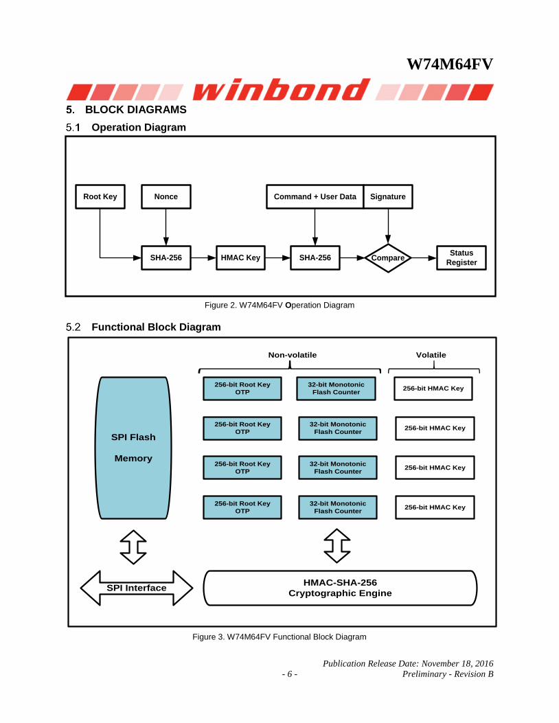
BLOCK DIAGRAMS
Operation Diagram
Figure 2. W74M64FV Operation Diagram
Functional Block Diagram
Figure 3. W74M64FV Functional Block Diagram
256-bit HMAC Key
256-bit Root Key
OTP
SPI Flash
Memory
HMAC-SHA-256
Cryptographic Engine
256-bit Root Key
OTP
256-bit Root Key
OTP
256-bit Root Key
OTP
32-bit Monotonic
Flash Counter
32-bit Monotonic
Flash Counter
32-bit Monotonic
Flash Counter
32-bit Monotonic
Flash Counter
256-bit HMAC Key
256-bit HMAC Key
256-bit HMAC Key
SPI Interface
Non-volatile Volatile
Command + User Data Signature
SHA-256HMAC Key CompareSHA-256
Nonce
Status
Register
Root Key

W74M64FV
- 7 -
FUNCTIONAL DESCRIPTIONS
Authentication Flash Operations
The W74M64FV is equipped with four 32-bit Monotonic Counters. Each set is accessible by the 8-bit Counter_Address that is HMAC-signed by the appropriate secret key. The SPI Flash Host controller uses the Monotonic Counter value to validate authenticity of the attached W74M device or modules which the W74M device resides.
The Authentication operation is based on the HMAC-SHA-256 cryptographic algorithm. HMAC-SHA-256 is a type of keyed hash algorithm that is constructed from the SHA-256 hash function and used as a Hash-based Message Authentication Code (HMAC). The HMAC process mixes a secret key with the message data, hashes the result with the hash function, mixes that hash value with the secret key again, and then applies the hash function a second time. The output hash is 256 bits in length.
The HMAC can be used by two parties that share a secret key to ensure the transmitted message remains secure. The sender computes the hash value for the original data and then sends the hash value plus original data, as a single message, to the receiver. The receiver recalculates the hash value on the received message and compares the hash value with the one sent by the sender. The receiver then reports the result to the status register. Figure 2 in Section 5, demonstrates this process.
6.1.1 Authentication Flash Initialization
The Authentication Flash operation is initialized by issuing the “Write Root Key Register” command. When this command is successfully received and executed, a 256-bit Root Key will be written into the Authentication Flash permanently, and the corresponding Monotonic Counter will also be initialized to 0. After the initialization procedure, the Root Key value can no longer be altered or accessed externally through the SPI interface. The initialized Monotonic Counter is ready to accept the commands from the authentication SPI Flash HOST controller.
Figure 3a. W74M64FV Initialization Flow Diagram
Un-initialized State
. Root Key Un-initialized (Blank)
. Monotonic Counter Un-initialized
Write Root Key Register
Read Status Register
Busy Status/Status Reset
Initialized State
. Root Key Established
. Monotonic Counter Initialized
W74M64FV
Publication Release Date: November 18, 2016
- 8 - Preliminary - Revision B
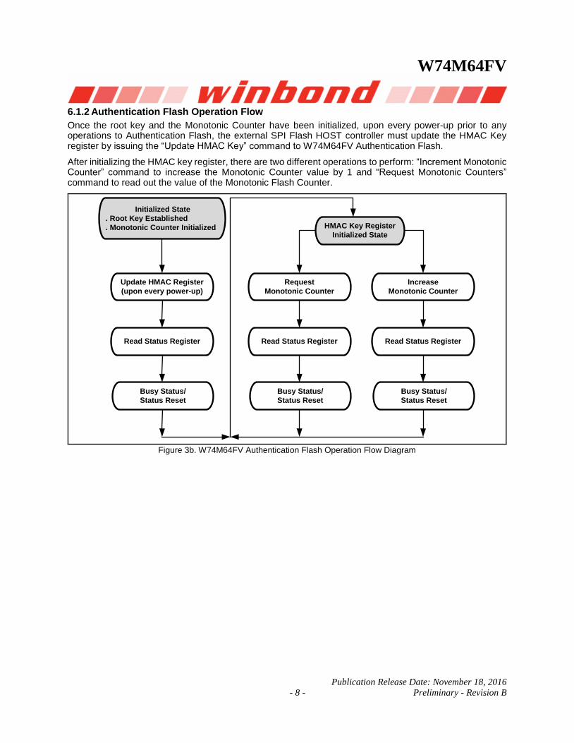
6.1.2 Authentication Flash Operation Flow
Once the root key and the Monotonic Counter have been initialized, upon every power-up prior to any operations to Authentication Flash, the external SPI Flash HOST controller must update the HMAC Key register by issuing the “Update HMAC Key” command to W74M64FV Authentication Flash.
After initializing the HMAC key register, there are two different operations to perform: “Increment Monotonic Counter” command to increase the Monotonic Counter value by 1 and “Request Monotonic Counters” command to read out the value of the Monotonic Flash Counter.
Figure 3b. W74M64FV Authentication Flash Operation Flow Diagram
Update HMAC Register
(upon every power-up)
Read Status Register
Busy Status/
Status Reset
Request
Monotonic Counter
Read Status Register
Busy Status/
Status Reset
Increase
Monotonic Counter
Read Status Register
Busy Status/
Status Reset
HMAC Key Register
Initialized State
Initialized State
. Root Key Established
. Monotonic Counter Initialized

W74M64FV
- 9 -
6.1.3 Operations Allowed / Disallowed to Authentication Flash
The operation to Authentication Flash is independent to the standard SPI Flash operations. The input command OP1 (9Bh) dedicated to Authentication Flash will initial internal operations after the authenticated command is accepted by the device. During the internal operation period, the BUSY bit in the Authentication Flash Status Register (bit 0) will be set to 1. The Authentication Flash internal operation cannot be suspended and can only be interrupted by the Device Reset command (66h+99h). While the operations dedicated to Authentication Flash is going on, other standard SPI Flash commands can be issued and executed. Please refer to the table below for details.
Operations Device Behavior
Authentication Flash
OP1 command
The input command OP1 will be ignored while an operation to Authentication Flash is on-going.
Read Authentication Flash Status/Data
OP2 command
The Status Register can be read out while an operation to Authentication Flash is on-going and this is the way to check if the operation has finished or not. If the BUSY bit of Status Register is set as 1, the data output following the Status Register is not valid.
Authentication Flash
Device Reset
The software reset sequence can be issued any time during the internal operations of the Authentication Flash. All volatile settings will be reset.
W74M64FV
Publication Release Date: November 18, 2016
- 10 - Preliminary - Revision B
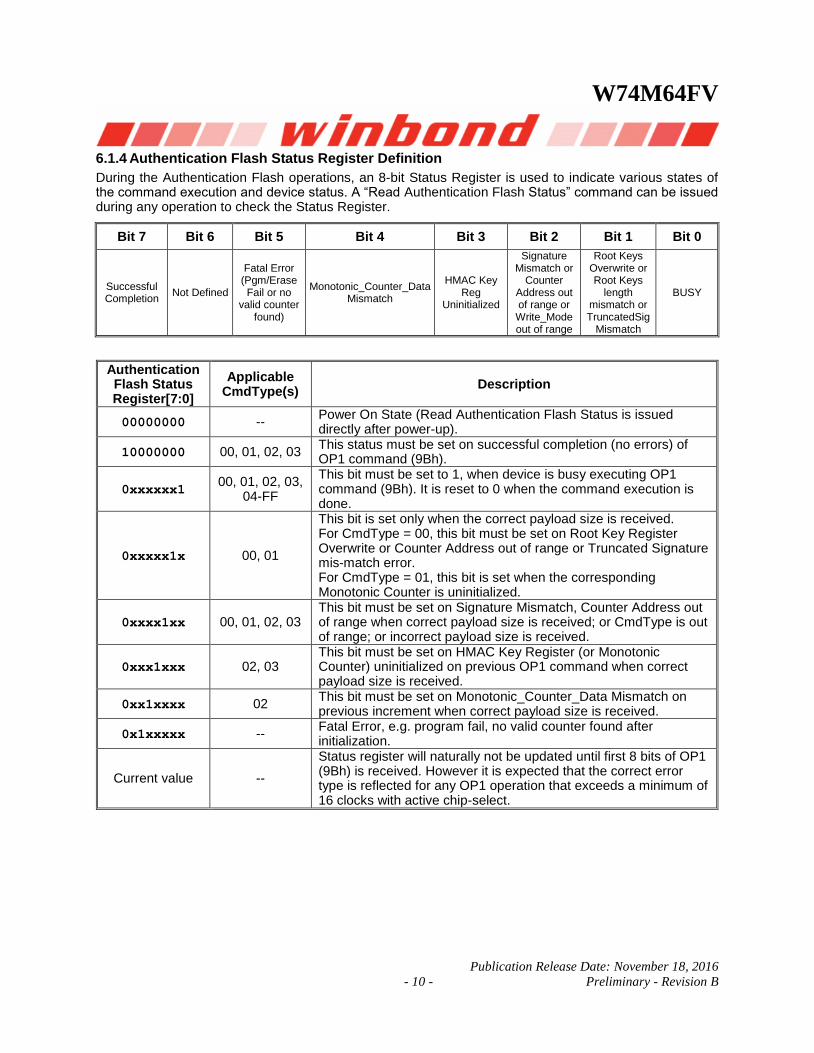
6.1.4 Authentication Flash Status Register Definition
During the Authentication Flash operations, an 8-bit Status Register is used to indicate various states of the command execution and device status. A “Read Authentication Flash Status” command can be issued during any operation to check the Status Register.
Bit 7 Bit 6 Bit 5 Bit 4 Bit 3 Bit 2 Bit 1 Bit 0
Successful Completion
Not Defined
Fatal Error (Pgm/Erase Fail or no
valid counter found)
Monotonic_Counter_Data Mismatch
HMAC Key Reg
Uninitialized
Signature Mismatch or
Counter Address out of range or Write_Mode out of range
Root Keys Overwrite or Root Keys
length mismatch or TruncatedSig
Mismatch
BUSY
Authentication Flash Status Register[7:0]
Applicable CmdType(s)
Description
00000000 -- Power On State (Read Authentication Flash Status is issued directly after power-up).
10000000 00, 01, 02, 03 This status must be set on successful completion (no errors) of OP1 command (9Bh).
0xxxxxx1 00, 01, 02, 03,
04-FF
This bit must be set to 1, when device is busy executing OP1 command (9Bh). It is reset to 0 when the command execution is done.
0xxxxx1x 00, 01
This bit is set only when the correct payload size is received. For CmdType = 00, this bit must be set on Root Key Register Overwrite or Counter Address out of range or Truncated Signature mis-match error. For CmdType = 01, this bit is set when the corresponding Monotonic Counter is uninitialized.
0xxxx1xx 00, 01, 02, 03 This bit must be set on Signature Mismatch, Counter Address out of range when correct payload size is received; or CmdType is out of range; or incorrect payload size is received.
0xxx1xxx 02, 03 This bit must be set on HMAC Key Register (or Monotonic Counter) uninitialized on previous OP1 command when correct payload size is received.
0xx1xxxx 02 This bit must be set on Monotonic_Counter_Data Mismatch on previous increment when correct payload size is received.
0x1xxxxx -- Fatal Error, e.g. program fail, no valid counter found after initialization.
Current value --
Status register will naturally not be updated until first 8 bits of OP1 (9Bh) is received. However it is expected that the correct error type is reflected for any OP1 operation that exceeds a minimum of 16 clocks with active chip-select.
W74M64FV
- 11 -
Instruction Set Tables
6.2.1 Instruction Set Table 2-1 (Authentication Flash Input Instruction, OP1)(1)
INSTRUCTION NAME
BYTE 0 BYTE 1
(CmdType) BYTE 2 BYTE 3(2)
Write
Root Key Register 9Bh 00h CounterAddr[7:0] Reserved[7:0]
Byte 4 - 35
RootKey[255:0]
Byte 36 - 63
TruncatedSign[223:0]
Update
HMAC Key Register 9Bh 01h CounterAddr[7:0] Reserved[7:0]
Byte 4 - 7
KeyData[31:0]
Byte 8 - 39
Signature[255:0]
Increment
Monotonic Counter 9Bh 02h CounterAddr[7:0] Reserved[7:0]
Byte 4 - 7
CounterData[31:0]
Byte 8 - 39
Signature[255:0]
Request
Monotonic Counter 9Bh 03h CounterAddr[7:0] Reserved[7:0]
Byte 4 - 15
Tag[95:0]
Byte 16 - 47
Signature[255:0]
Reserved Commands 9Bh 04h ~ FFh Reserved
6.2.2 Instruction Set Table 2-2 (Authentication Flash Output Instruction, OP2)(1)
INSTRUCTION NAME
BYTE 0 BYTE 1 BYTE 2 BYTE 3 - 14 BYTE 15 - 18 BYTE 19 - 50
Read Authentication
Flash Status / Data(3)(4) 96h Dummy (Status[7:0]) (Tag[95:0]) (CounterData[31:0]) (Signature[255:0])
6.2.3 Instruction Set Table 2-3 (Authentication Flash Reset Instruction)(1)
INSTRUCTION NAME
BYTE 0
Enable Reset 66h
Reset 99h
Notes:
1. All Authentication Flash instructions are in Standard SPI format. Each Input/Output Byte requires 8 clocks.
2. The Reserved[7:0] field for Authentication Flash OP1 must be all 0s (00000000’b).
3. The controller may terminate the Read Authentication Flash Status/Data instruction at any time without going through the entire data output sequence.
4. When BUSY=1, from Byte-3 and beyond, the device will output the Authentication Flash Status[7:0] value continuously until /CS terminates the instruction. The device will not output Tag, CounterData & Signature fields when BUSY=1. Once BUSY becomes 0, another OP2 command must be issued to read out the correct Tag, CounterData & Signature fields.

W74M64FV
Publication Release Date: November 18, 2016
- 12 - Preliminary - Revision B
Instruction Descriptions
6.3.1 Write Root Key Register (9Bh + 00h)
This command is used by the SPI Flash HOST Controller to initialize the Root Key Register corresponding to the received Counter Address with the received Root Key. It is expected to be used in an OEM manufacturing environment when the SPI Flash HOST Controller and SPI Flash are powered together for the first time.
After the command is issued on the interface the Authentication Flash must ensure that the received transaction is error free. This includes checking following conditions:
Payload size is correct. (including OP1 is 64 bytes)
Counter Address falls within the range of supported counters.
The Root Key Register corresponding to the requested Counter Address was previously uninitialized. [Root_Key_Reg_Init_State[Monotonic_Counter_Address] = 0xFFh]
Truncated signature field is the same as least significant 224 bits of HMAC-SHA-256 based signature computed based on received input parameters.
If the received transaction is error free, the Authentication Flash successfully executes the command and posts “successful completion” in the Authentication Flash Status Register. This command must be executed to ensure that power cycling in the middle of command execution is properly handled. This requires that the internal state tracking the root key register initialization is written as the last operation of the command execution. (Root_Key_Reg_Init_State[Monotonic_Counter_Address] = 0]
Root Key Register Write with root key is = 256’hFF…FF is used as a temporary key. When this request is received error-free Root_Key_Reg_Init_State[Monotonic_Counter_Address] is not affected. Instead only the corresponding Monotonic Counter is initialized to 0 if previously uninitialized. This state is tracked as separate state using MC_Init_State[Monotonic_Counter_Address]. This state is used to leave the Monotonic Counter at the current value when an error free Root Key Register Write operation is received. (Both 256’hFF..FF and non 256’hFF..FF)
Once this command is successfully executed with a non 256’hFF..FF Root Key, the device will not accept the “Write Root Key Register” command any more, and the Root Key value cannot be read out by any instructions.
Figure 4. Write Root Key Register Instruction
/CS
CLK
DO
DIO Counter Addr
[7:0]Reserved[7:0] Root Key[255:0] Truncated Sign[223:0]
0 1 2 3 4 5 6 7 8 910
11
12
13
14
15
16
17
18
19
20
21
22
23
24
25
26
27
28
29
30
31
32
33
34
35
287
286
285
284
291
290
289
288
511
510
509
508Mode 3
Mode 0
Instruction (9Bh) CMD Type (00h)
Mode 3
Mode 0

W74M64FV
- 13 -
6.3.2 Update HMAC Key (9Bh + 01h)
This command is used by the SPI Flash Controller to update the HMAC-Key register corresponding to the received Counter Address with a new HMAC key calculated based on received input. This command must be issued once only on every power cycle event on the interface. This allows the HMAC key storage to be implemented using volatile memory. Status register busy indication is expected to indicate busy for double the amount of Read_Counter_Polling_Delay specified in SFDP table since this command performs two distinct HMAC-SHA-256 computations.
After the command is issued on the interface the Authentication Flash must ensure that the received transaction is error free. This includes checking following conditions:
Payload size is correct. (including OP1 = 40 bytes)
Counter Address falls within the range of supported counters.
The Monotonic Counter corresponding to the requested Counter Address was previously initialized.
Signature matches the HMAC-SHA-256 based signature computed based on received input parameters. This command performs two HMAC-SHA-256 operations.
If the received transaction is error free, the Authentication Flash successfully executes the command and posts “successful completion” in the Authentication Flash Status Register.
If the received transaction has errors, the Authentication Flash does not execute the transaction and posts the corresponding error in the Authentication Flash Status Register.
Reserved[7:0] Key Data[31:0] Signature[255:0]
/CS
CLK
DO
DIO
Mode 3
Mode 0
0 1 2 3 4 5 6 7 8 910
11
12
13
14
15
16
17
18
19
20
21
22
23
24
25
26
27
28
29
30
31
60
61
62
63
67
66
65
64
319
318
317
316
Instruction (9Bh)
32
33
34
35 Mode 3
Mode 0
CMD Type (01h)
Counter Addr
[7:0]
Figure 5. Update HMAC Key Register Instruction

W74M64FV
Publication Release Date: November 18, 2016
- 14 - Preliminary - Revision B
6.3.3 Increment Monotonic Counter (9Bh + 02h)
This command is used by the SPI Flash Controller to increment the Monotonic Counter by 1 inside the Authentication Flash.
After the command is issued on the interface the Authentication Flash must ensure that the received transaction is error free. This includes checking following conditions:
Payload size is correct. (including OP1 = 40 bytes)
Counter Address falls within the range of supported counters.
The Monotonic Counter corresponding to the requested Counter Address was previously initialized.
The HMAC Key Register corresponding to the requested Counter Address was previously initialized.
The requested Signature matches the HMAC-SHA-256 based signature computed based on received input parameters.
The received Monotonic_Counter_Data matches the current value of the counter read from the SPI Flash.
If the received transaction is error free, the Authentication Flash successfully executes the command and posts “successful completion” in the Authentication Flash Status Register. The increment counter implementation should make sure that the counter increment operation is performed in a power glitch aware manner.
Reserved[7:0] Counter Data[31:0] Signature[255:0]
/CS
CLK
DO
DIO
Instruction (9Bh)
0 1 2 3 4 5 6 7 8 910
11
12
13
14
15
16
17
18
19
20
21
22
23
24
25
26
27
28
29
30
31
60
61
62
63
67
66
65
64
319
318
317
316
32
33
34
35 Mode 3
Mode 0
Mode 3
Mode 0
CMD Type (02h)
Counter Addr
[7:0]
Figure 6. Increment Monotonic Counter Instruction

W74M64FV
- 15 -
6.3.4 Request Monotonic Counter (9Bh + 03h)
This command is used by the SPI Flash Controller to request the Monotonic Counter value inside the Authentication Flash.
After the command is issued on the interface the Authentication Flash must ensure that the received transaction is error free. This includes checking following conditions:
Payload size is correct. (including OP1 = 48 bytes)
Counter Address falls within the range of supported counters.
The Monotonic Counter corresponding to the requested Counter Address was previously initialized.
The HMAC Key Register corresponding to the requested Counter Address was previously initialized.
The requested Signature matches the HMAC-SHA-256 based signature computed based on received input parameters.
If the received transaction is error free, the Authentication Flash successfully executes the command and posts “successful completion” in the Authentication Flash Status Register. In response to this command, the SPI flash reads the Monotonic Counter addressed by counter address. It calculates HMAC-SHA-256 signatures the second time, based on following parameters.
HMAC Message[127:0] = Tag [95:0], Counter_Data_Read[31:0]
HMAC Key[255:0] = HMAC_Key_Register[Monotonic_Counter_Address][255:0]
Reserved[7:0] Tag[95:0] Signature[255:0]
Instruction (9Bh)
/CS
CLK
DO
DIO
Mode 3
Mode 0
0 1 2 3 4 5 6 7 8 910
11
12
13
14
15
16
17
18
19
20
21
22
23
24
25
26
27
28
29
30
31
124
125
126
127
131
130
129
128
383
382
381
380
32
33
34
35 Mode 3
Mode 0
CMD Type (03h)
Counter Addr
[7:0]
Figure 7. Request Monotonic Counter Instruction
6.3.5 Reserved Authentication Flash Device Commands (9Bh + 04h~FFh)
If the SPI Flash Controller issues any of the reserved command-types, the Authentication Flash must return Error status in the Authentication Flash Status Register. It asserts bit 2 to indicate that a reserved command-type was issued.

W74M64FV
Publication Release Date: November 18, 2016
- 16 - Preliminary - Revision B
6.3.6 Read Authentication Flash Device Status / Data (96h)
This command is used by the SPI Flash Controller to read the Authentication Flash status from any previously issued OP1 command. In addition, if previous OP1 command is Request Monotonic Counter and if SPI Flash returns successful completion (BUSY=0) in the Authentication Flash Status Register, then it must also return valid values in the Tag, Monotonic_Counter_Data and Signature field. If there’re other error flags, the values returned in Tag, Counter and Signature field are invalid. The controller may abort the read prematurely prior to completely reading the entire payload. This may occur when the controller wants to simply read the Authentication Flash status or when it observes an error being returned in the Authentication Flash status field. The controller may also continue reading past the defined payload size of 49 bytes. Since this is an error condition, the SPI Flash may return any data past the defined payload size. The controller must ignore the data.
Status[7:0] Counter Data[31:0]Tag[95:0] Signature[255:0]
/CS
CLK
DO
DIO
Mode 3
Mode 0
Instruction (96h)
0 1 2 3 4 5 6 7 8 910
11
12
13
14
15
16
17
18
19
20
21
22
23
24
25
26
116
150
151
155
154
153
152
407
406
405
404
117
118
119
120
121 Mode 3
Mode 0
Dummy Bits[7:0]
High Impedance
Don’t Care
Figure 8a. Read Authentication Flash Data Instruction (BUSY=0)
When BUSY=1, from Byte-3 and beyond, the device will output the Authentication Flash Status[7:0] value continuously until /CS terminates the instruction. The device will not output Tag, CounterData & Signature fields when BUSY=1. Once BUSY becomes 0, another OP2 command must be issued to read out the correct Tag, CounterData & Signature fields.
/CS
CLK
DO
DIO
Mode 3
Mode 0
Instruction (96h)
0 1 2 3 4 5 6 7 8 910
11
12
13
14
15
16
17
18
19
20
21
22
23
24
25
26
116
150
151
155
154
153
152
407
406
405
404
117
118
119
120
121 Mode 3
Mode 0
Dummy Bits[7:0]
High Impedance
Don’t Care
Status[7:0] Status[7:0] Status[7:0] Status[7:0]
Figure 8b. Read Authentication Flash Data Instruction (BUSY=1)

W74M64FV
- 17 -
6.3.7 Enable Reset (66h) and Reset Device (99h)
Because of the small package and the limitation on the number of pins, the Authentication Flash provide a software Reset instruction. Once the Reset instruction is accepted, any on-going internal operations will be terminated and the device will return to its default power-on state and lose all the current volatile settings, such as Volatile Status Register bits.
To avoid accidental reset, both instructions must be issued in sequence. Any other commands other than “Reset (99h)” after the “Enable Reset (66h)” command will disable the “Reset Enable” state. A new sequence of “Enable Reset (66h)” and “Reset (99h)” is needed to reset the device. Once the Reset command is accepted by the device, the device will take approximately tRST=30us to reset. During this period, no command will be accepted.
Data corruption may happen if there is an on-going when Reset command sequence is accepted by the device. It is recommended to check the BUSY bit Authentication Flash Register before issuing the Reset command sequence.
Figure 9. Enable Reset and Reset Instruction Sequence
Mode 0
Mode 3 0 1 2 3 4 5 6 7
Instruction (99h)
Mode 0
Mode 3
/CS
CLK
DI
(IO0)
DO
(IO1)
Mode 0
Mode 3 0 1 2 3 4 5 6 7
Instruction (66h)
High Impedance

W74M64FV
Publication Release Date: November 18, 2016
- 18 - Preliminary - Revision B
ELECTRICAL CHARACTERISTICS(1)
Absolute Maximum Ratings (2)
PARAMETERS SYMBOL CONDITIONS RANGE UNIT
Supply Voltage VCC –0.6 to VCC+0.4 V
Voltage Applied to Any Pin VIO Relative to Ground –0.6 to VCC+0.4 V
Transient Voltage on any Pin VIOT <20nS Transient
Relative to Ground –2.0V to VCC+2.0V V
Storage Temperature TSTG –65 to +150 °C
Lead Temperature TLEAD See Note (3) °C
Electrostatic Discharge Voltage VESD Human Body Model(4) –2000 to +2000 V
Notes:
1. Specification for W74M64FV is preliminary. See preliminary designation at the end of this document.
2. This device has been designed and tested for the specified operation ranges. Proper operation outside of these levels is not guaranteed. Exposure to absolute maximum ratings may affect device reliability. Exposure beyond absolute maximum ratings may cause permanent damage.
3. Compliant with JEDEC Standard J-STD-20C for small body Sn-Pb or Pb-free (Green) assembly and the European directive on restrictions on hazardous substances (RoHS) 2002/95/EU.
4. JEDEC Std JESD22-A114A (C1=100pF, R1=1500 ohms, R2=500 ohms).
Operating Ranges
PARAMETER SYMBOL CONDITIONS SPEC
UNIT MIN MAX
Supply Voltage VCC FR = 80MHz 2.7 3.6 V
Ambient Temperature, Operating TA Industrial –40 +85 °C
W74M64FV
- 19 -
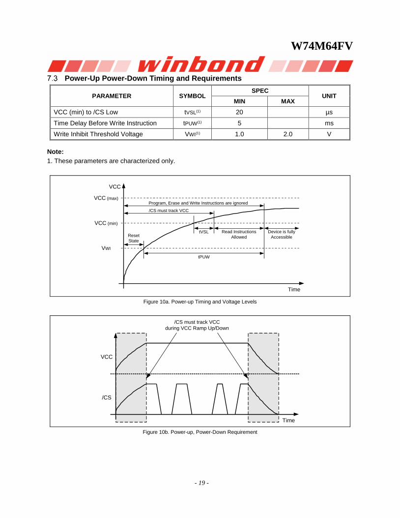
Power-Up Power-Down Timing and Requirements
PARAMETER SYMBOL SPEC
UNIT MIN MAX
VCC (min) to /CS Low tVSL(1) 20 µs
Time Delay Before Write Instruction tPUW(1) 5 ms
Write Inhibit Threshold Voltage VWI(1) 1.0 2.0 V
Note:
1. These parameters are characterized only.
Figure 10a. Power-up Timing and Voltage Levels
Figure 10b. Power-up, Power-Down Requirement
VCC
tVSL Read Instructions
Allowed
Device is fully
Accessible
tPUW
/CS must track VCC
Program, Erase and Write Instructions are ignored
Reset
State
VCC (max)
VCC (min)
VWI
Time
VCC
Time
/CS must track VCC
during VCC Ramp Up/Down
/CS
W74M64FV
Publication Release Date: November 18, 2016
- 20 - Preliminary - Revision B
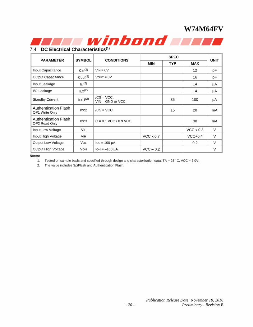
DC Electrical Characteristics(1)
PARAMETER SYMBOL CONDITIONS SPEC
UNIT MIN TYP MAX
Input Capacitance CIN(2) VIN = 0V 12 pF
Output Capacitance Cout(2) VOUT = 0V 16 pF
Input Leakage ILI(2) ±4 µA
I/O Leakage ILO(2) ±4 µA
Standby Current ICC1(2) /CS = VCC, VIN = GND or VCC
35 100 µA
Authentication Flash
OP1 Write Only ICC2 /CS = VCC 15 20 mA
Authentication Flash OP2 Read Only
ICC3 C = 0.1 VCC / 0.9 VCC 30 mA
Input Low Voltage VIL VCC x 0.3 V
Input High Voltage VIH VCC x 0.7 VCC+0.4 V
Output Low Voltage VOL IOL = 100 µA 0.2 V
Output High Voltage VOH IOH = –100 µA VCC – 0.2 V
Notes:
1. Tested on sample basis and specified through design and characterization data. TA = 25° C, VCC = 3.0V.
2. The value includes SpiFlash and Authentication Flash.
W74M64FV
- 21 -
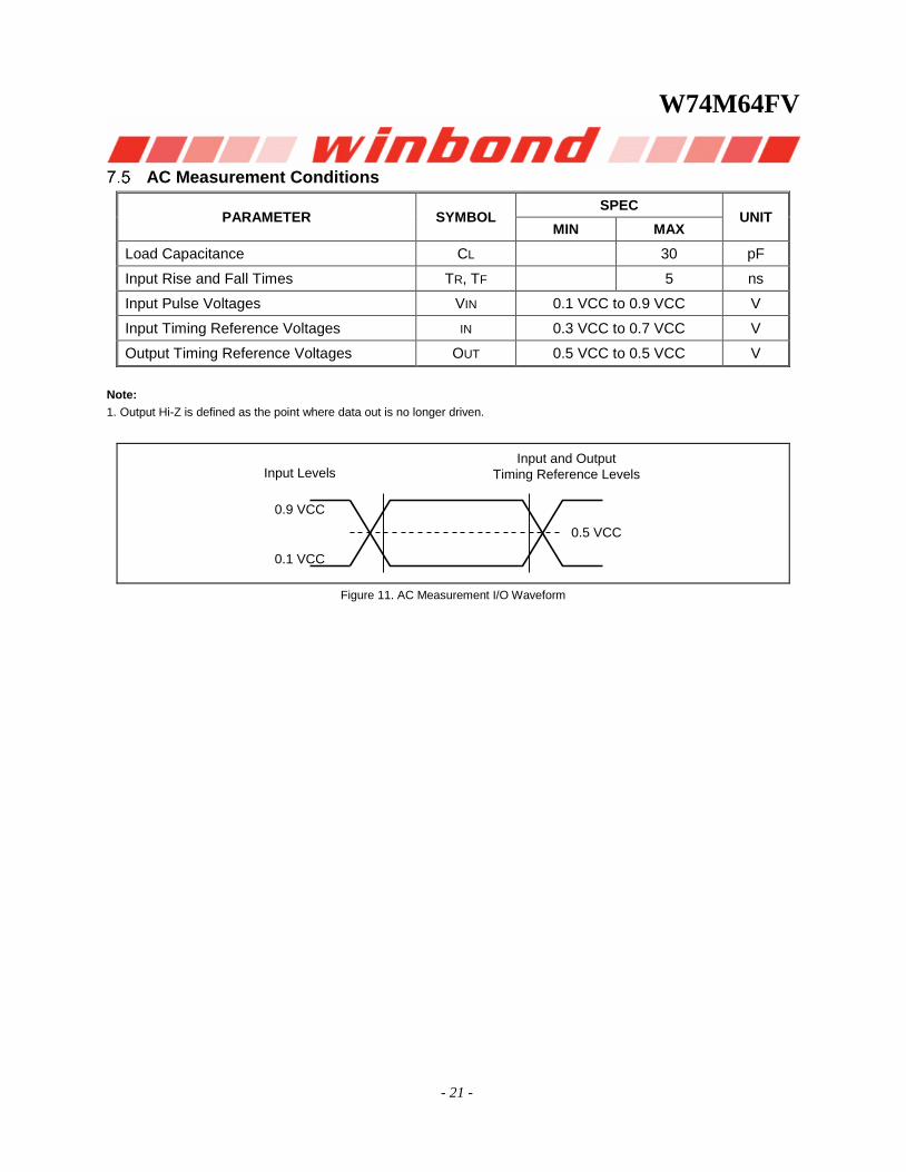
AC Measurement Conditions
PARAMETER SYMBOL SPEC
UNIT MIN MAX
Load Capacitance CL 30 pF
Input Rise and Fall Times TR, TF 5 ns
Input Pulse Voltages VIN 0.1 VCC to 0.9 VCC V
Input Timing Reference Voltages IN 0.3 VCC to 0.7 VCC V
Output Timing Reference Voltages OUT 0.5 VCC to 0.5 VCC V
Note:
1. Output Hi-Z is defined as the point where data out is no longer driven.
Figure 11. AC Measurement I/O Waveform
Input and Output
Timing Reference LevelsInput Levels
0.9 VCC
0.1 VCC
0.5 VCC

W74M64FV
Publication Release Date: November 18, 2016
- 22 - Preliminary - Revision B
AC Electrical Characteristics(3,4)
DESCRIPTION SYMBOL ALT SPEC
UNIT MIN TYP MAX
Clock frequency for OP1/OP2 FR fC D.C. 80 MHz
Clock High, Low Time tCLH,
tCLL(1)
5 ns
Clock Rise Time peak to peak tCLCH(2) 0.1 V/ns
Clock Fall Time peak to peak tCHCL(2) 0.1 V/ns
/CS Active Setup Time relative to CLK tSLCH tCSS 5 ns
/CS Not Active Hold Time relative to CLK tCHSL 5 ns
Data In Setup Time tDVCH tDSU 2 ns
Data In Hold Time tCHDX tDH 5 ns
/CS Active Hold Time relative to CLK tCHSH 3 ns
/CS Not Active Setup Time relative to CLK tSHCH 3 ns
/CS Deselect Time tSHSL tCSH 50 ns
Output Disable Time / Output Disable Time tSHQZ tDIS 7 / 8.5 ns
Clock Low to Output Valid 2.7V-3.0V / 3.0V-3.6V
tCLQV1 tV1 7 / 6 ns
Clock Low to Output Valid for Authentication Flash OP2 command 2.7V-3.0V / 3.0V-3.6V
tCLQV2 tV2 8.5 / 7.5 ns
Output Hold Time tCLQX tHO 2 ns
Continued – next page

W74M64FV
- 23 -
AC Electrical Characteristics (cont’d)
DESCRIPTION SYMBOL ALT SPEC
UNIT MIN TYP MAX
/CS High to Standby Mode tRES1(2) 3 µs
/CS High to next Instruction after Reset tRST(2) 30 µs
Write Root Key Register tKEY 170 250 µs
Update HMAC Key Register tHMAC 50 75 µs
Increment Monotonic Counter tINC1 80 200 µs
Increment Monotonic Counter (Counter Switching) tINC2 75 250 ms
Authentication Flash Request Monotonic Counter tREQ 80 120 µs
Notes:
1. Clock high + Clock low must be less than or equal to 1/fC.
2. Value guaranteed by design and/or characterization, not 100% tested in production.
3. Tested on sample basis and specified through design and characterization data. TA = 25° C, VCC = 3.0V.
W74M64FV
Publication Release Date: November 18, 2016
- 24 - Preliminary - Revision B
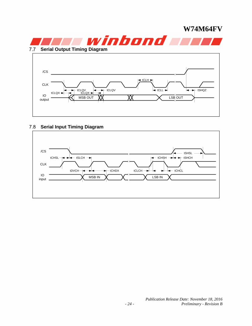
Serial Output Timing Diagram
Serial Input Timing Diagram
/CS
CLK
IO
output
tCLQXtCLQV
tCLQXtCLQV tSHQZtCLL
LSB OUT
tCLH
MSB OUT
/CS
CLK
IO
input
tCHSL
MSB IN
tSLCH
tDVCH tCHDX
tSHCHtCHSH
tCLCH tCHCL
LSB IN
tSHSL

W74M64FV
- 25 -
PACKAGE SPECIFICATIONS
8-Pin SOIC 208-mil (Package Code SS)
Symbol Millimeters Inches
Min Nom Max Min Nom Max
A 1.75 1.95 2.16 0.069 0.077 0.085
A1 0.05 0.15 0.25 0.002 0.006 0.010
A2 1.70 1.80 1.91 0.067 0.071 0.075
b 0.35 0.42 0.48 0.014 0.017 0.019
C 0.19 0.20 0.25 0.007 0.008 0.010
D 5.18 5.28 5.38 0.204 0.208 0.212
D1 5.13 5.23 5.33 0.202 0.206 0.210
E 5.18 5.28 5.38 0.204 0.208 0.212
E1 5.13 5.23 5.33 0.202 0.206 0.210
e 1.27 BSC 0.050 BSC
H 7.70 7.90 8.10 0.303 0.311 0.319
L 0.50 0.65 0.80 0.020 0.026 0.031
y --- --- 0.10 --- --- 0.004
θ 0° --- 8° 0° --- 8°
θ

W74M64FV
Publication Release Date: November 18, 2016
- 26 - Preliminary - Revision B
Ordering Information
Notes:
1. The “W” prefix is not included on the part marking.
2. Standard bulk shipments are in Tube (shape E). Please specify alternate packing method, such as Tape and Reel (shape T) or Tray (shape S), when placing orders.
W(1) 74M 64F V SS I
W = Winbond
74M = SpiFlash Serial Flash Memory with Dual/Quad I/O and Secure Authentication
64F = 64M-bit
V = 2.7V to 3.6V
SS = 8-pin SOIC 208-mil
I = Industrial (-40°C to +85°C)
(2)
Q = Green Package (Lead-free, RoHS Compliant, Halogen-free (TBBA), Antimony-Oxide-free Sb2O3)
with QE=1 in Status Register-2
V SS I(1)

W74M64FV
- 27 -
Valid Part Numbers and Top Side Marking
The following table provides the valid part numbers for the W74M64FV. Please contact Winbond for specific availability of different package types. Winbond Authentication Flash use a 12-digit Product Number for ordering. However, due to limited space, the Top Side Marking on all packages uses an abbreviated 10-digit number.
PACKAGE TYPE DENSITY PRODUCT NUMBER TOP SIDE MARKING
SS SOIC-8 208-mil
64M-bit W74M64FVSSIQ 74M64FVSIQ
Note:
Contact Winbond for other package options.
GENERAL INSTRUCTIONS
Digit number for all Spi-Flash features, DC and AC parameters, and functions of this product, please refer to the datasheet of W25Q64FV which can be found on Winbond web site http:// www.winbond.com or www.spiflash.com.

W74M64FV
Publication Release Date: November 18, 2016
- 28 - Preliminary - Revision B
REVISION HISTORY
VERSION DATE PAGE DESCRIPTION
A 06/06/2016 New Create Preliminary
B 11/18/2016 All New datasheet format
Enrich authentication flash operation method
Preliminary Designation
The “Preliminary” designation on a Winbond datasheet indicates that the product is not fully characterized. The specifications are subject to change and are not guaranteed. Winbond or an authorized sales representative should be consulted for current information before using this product.
Trademarks
Winbond is a trademark of Winbond Electronics Corporation. All other marks are the property of their respective owner.
Important Notice
Winbond products are not designed, intended, authorized or warranted for use as components in systems or equipment intended for surgical implantation, atomic energy control instruments, airplane or spaceship instruments, transportation instruments, traffic signal instruments, combustion control instruments, or for other applications intended to support or sustain life. Furthermore, Winbond products are not intended for applications wherein failure of Winbond products could result or lead to a situation wherein personal injury, death or severe property or environmental damage could occur. Winbond customers using or selling these products for use in such applications do so at their own risk and agree to fully indemnify Winbond for any damages resulting from such improper use or sales.
Information in this document is provided solely in connection with Winbond products. Winbond reserves the right to make changes, corrections, modifications or improvements to this document and the products and services described herein at any time, without notice.


