M820-00 T828 Fault Finding D4.1 Copyright TEL 01/07/00 4 T828 Fault Finding Caution: This equipment contains CMOS devices which are susceptible to dam- age from static charges. Refer to Section 1.2 in Part A for more infor- mation on anti-static procedures when handling these devices. The following test procedures and fault finding flow charts may be used to help locate a hardware problem, however they are by no means a complete fault finding procedure. If you still cannot trace the fault after progressing through them in a logical manner, contact your nearest Tait Dealer or Customer Service Organisation. If necessary, you can get additional technical help from Customer Support, Radio Systems Division, Tait Electronics Ltd, Christchurch, New Zealand (full contact details are on page 2). Refer to Section 5 where the parts lists, grid reference index and diagrams will provide detailed information on identifying and locating components. The following topics are covered in this section. Section Title Page 4.1 Visual Checks 4.3 4.2 Component Checks 4.3 4.3 DC Checks 4.3 4.4 4.4.1 4.4.2 RF Checks General PA Faults 4.4 4.4 4.4 4.5 Voltage Chart 4.5 4.6 4.6.1 4.6.2 Fault Finding Charts PA Power Control 4.6 4.6 4.7 4.7 Replacing RF Power Transistors 4.8 4.8 Removing The PCB From The Heatsink 4.9 Figure Title Page 4.1 T828 Test Break Point Location 4.4
Transcript
M820-00 T828 Fault Finding D4.1
Copyright TEL 01/07/00
4 T828 Fault Finding
Caution: This equipment contains CMOS devices which are susceptible to dam-age from static charges. Refer to Section 1.2 in Part A for more infor-mation on anti-static procedures when handling these devices.
The following test procedures and fault finding flow charts may be used to help locate ahardware problem, however they are by no means a complete fault finding procedure.If you still cannot trace the fault after progressing through them in a logical manner,contact your nearest Tait Dealer or Customer Service Organisation. If necessary, youcan get additional technical help from Customer Support, Radio Systems Division, TaitElectronics Ltd, Christchurch, New Zealand (full contact details are on page 2).
Refer to Section 5 where the parts lists, grid reference index and diagrams will providedetailed information on identifying and locating components.
The following topics are covered in this section.
Section Title Page
4.1 Visual Checks 4.3
4.2 Component Checks 4.3
4.3 DC Checks 4.3
4.4
4.4.1
4.4.2
RF Checks
General
PA Faults
4.4
4.4
4.4
4.5 Voltage Chart 4.5
4.6
4.6.1
4.6.2
Fault Finding Charts
PA
Power Control
4.6
4.6
4.7
4.7 Replacing RF Power Transistors 4.8
4.8 Removing The PCB From The Heatsink 4.9
Figure Title Page
4.1 T828 Test Break Point Location 4.4
D4.2 T828 Fault Finding M820-00
01/07/00 Copyright TEL
M820-00 T828 Fault Finding D4.3
Copyright TEL 01/07/00
4.1 Visual Checks
Remove the side cover from the T828 and inspect the PCB for damaged or brokencomponents, paying particular attention to the surface mounted devices (SMDs).Also check for defective solder joints.
Refer to Section 4.7, Section 4.8 and Section 3 of Part A for more details on repairand replacement of components.
4.2 Component Checks
If you suspect a transistor is faulty, you can assess its performance by measuring the for-ward and reverse resistance of the junctions. Unless the device is completely desol-dered, first make sure that the transistor is not shunted by some circuit resistance. Use agood quality EVM (e.g. Fluke 75) for taking the measurements (or a 20k ohm/V or bet-ter multimeter, using only the medium or low resistance ranges).
The collector current drawn by multi-junction transistors is a further guide to their per-formance.
If an IC is suspect, the most reliable check is to measure the DC operating voltages. Dueto the catastrophic nature of most IC failures, the pin voltages will usually be markedlydifferent from the recommended values in the presence of a fault. The recommendedvalues can be obtained from either the circuit diagram or the component data catalogue.
4.3 DC Checks
Note: No RF power is to be applied during these checks.
Check that +13.8V is present on the collectors of Q1, Q2, Q3 and Q4. Make thismeasurement when the transmitter is not keyed.
Check that +13.8V is present at pin 4 of IC1 and pin 8 of IC3.
Check that 7.0V is present at the output of regulator IC2.
D4.4 T828 Fault Finding M820-00
01/07/00 Copyright TEL
4.4 RF Checks
4.4.1 General
You can measure in-circuit RF levels around Q1 and Q2 with an RF probe on which theearth lead has been shortened to a minimum (i.e. 13mm); refer to the PA Fault FindingChart (Section 4.6.1). You must measure all other stages with a power meter at the 50Ωpoints in the circuit.
For problems with the power control circuitry, refer to the Power Control Fault FindingChart (Section 4.6.2).
4.4.2 PA Faults
If a PA fault has occurred, or is suspected, it is easier to find if the various stages are iso-lated by use of the test breaks (refer to Figure 4.1) and each stage analysed individually.Eight 50 ohm test break points have been included throughout the RF circuitry to enableindividual transistor stages to be tested.
Testing may be performed by removing the solder short across the test break and sol-dering a 50 ohm test lead to the appropriate signal and earth pads.
Note 1: Use good quality 50Ω coax for the "flying" test leads.
Note 2: Ensure each output is terminated in a 50Ω load of the correct power rating.
Figure 4.1 T828 Test Break Point Location
TB6
TB7
TB3
TB5
TB4
TB2
TB1
TB8
M820-00 T828 Fault Finding D4.5
Copyright TEL 01/07/00
4.5 Voltage Chart
Test conditions:
• typical DC voltages measured with Fluke 77 DVM
• supply voltage 13.8V at socket
• transmitter unkeyed
• allow ±20% for spread of transistor characteristics.
Device Emitter Base Collector
Q1
Q2
Q3
Q4
Q11
Q13
Q15
Q16
0.0V
0.0V
0.0V
0.0V
1.8V
0.0V
13.0V
13.8V
0.0V
0.0V
0.0V
0.0V
2.2V
0.0V
13.6V
13.6V
13.0V
13.8V
13.8V
13.8V
5.9V
5.9V
13.6V
13.0V
D4.6 T828 Fault Finding M820-00
01/07/00 Copyright TEL
4.6 Fault Finding Charts
4.6.1 PA
Repair exciter.
Check for shortson base of Q1,
around resistorson base, chips,input matchingcomponents,& input pad.
Check >13V presentat collector of Q1.Check for shortsaround resistors& chips on base.
Check for shorts onbase of Q3 & Q4.Check collectorvoltage of Q2.
Check power outputof driver amp.
Check for shorts onbase of Q3 & Q4"split amplifiers".
Check output of each stage.Check output filter.
N
N
N
Check power controltransistors Q16 & Q15.
IC1 pin 8 high (>13V)?Check input voltages
at pin 10.
Q2 faulty (MRF234).
Q3 & Q4 faulty(SD1019).
Y
Key exciter.Input power to PA 0.8W?
>0.7V RF presentat base of Q1?
>0.9V RF presentat base of Q2?
>1.0V RF presentat base of Q3 & Q4?
>60W RF outputat "N" connector?
Y
N
PA OK.
Y
Y
Y
N
N
N
N
Y
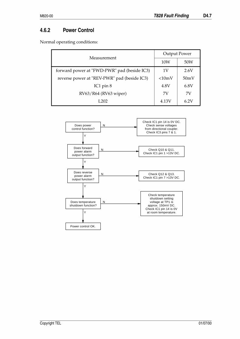
M820-00 T828 Fault Finding D4.7
Copyright TEL 01/07/00
4.6.2 Power Control
Normal operating conditions:
MeasurementOutput Power
10W 50W
forward power at "FWD-PWR" pad (beside IC3)
reverse power at "REV-PWR" pad (beside IC3)
IC1 pin 8
RV63/R64 (RV63 wiper)
L202
1V
<10mV
4.8V
7V
4.13V
2.6V
50mV
6.8V
7V
6.2V
Does forwardpower alarm
output function?
Check Q10 & Q11.Check IC1 pin 1 >13V DC.
Does reversepower alarm
output function?
Check Q12 & Q13.Check IC1 pin 7 >13V DC.
Check temperatureshutdown settingvoltage at TP1 is
approx. 150mV DC.Check IC1 pin 14 is 0Vat room temperature.
Does temperatureshutdown function?
Check IC1 pin 14 is 0V DC.Check sense voltages
from directional coupler.Check IC3 pins 7 & 1.
Does powercontrol function?
Power control OK.
N
N
N
N
Y
Y
Y
Y
D4.8 T828 Fault Finding M820-00
01/07/00 Copyright TEL
4.7 Replacing RF Power Transistors
Caution: Failure to comply with the following procedure can result in failure ofthe device due to poor heatsinking, or worse, can endanger the healthof the assembler if the beryllium oxide die carrier is smashed duringassembly.
Caution: As the location of certain components in the PA is critical to perform-ance, it is important that any components removed or disturbed arerefitted in exactly the same position. Before attempting to remove atransistor, note the location of any other components that will alsoneed to be removed. Replacing each component in its original locationwill help to maintain the performance of the PA.
Caution: Do not apply too much heat or pressure to the PCB pads and tracks asyou may damage them or lift them from the PCB, causing permanentdamage to the PA.
Desolder and remove the components from around the transistor.
Desolder the transistor tabs by heating with a soldering iron and lifting awayfrom the PCB with a screwdriver or thin stainless steel spike. Unscrew the transis-tor stud nut and remove the device.
Remove any excess solder from the PCB pads with solder wick.
Trim the tabs of the replacement transistor so that the device sits neatly on thePCB pads provided.
Lightly tin the underside of the transistor tabs.
Apply a small amount of heatsink compound (Dow-Corning 340 or equivalent) tothe transistor mounting surface. Sufficient compound should be used to ensurean even film over the entire mounting surface.
Place the transistor on the PCB in the correct orientation and ensure the tabs areflush to the surface.
Lightly solder one tab to the PCB, then torque down the retaining nut to the cor-rect torque (0.7Nm/6in.lbf.).
Caution: Do not solder all the tabs before torquing down otherwise the devicemay be broken.
Solder all transistor tabs to the PCB.
Replace each component in exactly the same position as noted previously.
M820-00 T828 Fault Finding D4.9
Copyright TEL 01/07/00
4.8 Removing The PCB From The Heatsink
Note: This is a lengthy procedure and should be considered only after all otherchecks have been carried out. There are no components on the bottom of thePCB.
Remove the harmonic filter shield lid.
Remove the 50 ohm output N-type connector by unscrewing it from the heatsinkcasting and desoldering it from the PCB.
Unplug the 50 ohm input coaxial cable from the PCB, unscrew the BNC connectorfrom the heatsink, and remove the connector and cable (cutting cable ties asrequired).
Desolder the positive and negative power feed wires from the PCB.
Desolder the alarm and metering wires from the PCB.
Remove the 2 screws securing the D-range connector and PCB to the heatsink andwithdraw the assembly and wires from the heatsink (cutting cable ties asrequired).
Remove the transistor stud nuts.
Remove the mounting screws for the TO-220 devices: R230, R231 and Q16.
Remove the 10 PCB retaining screws.
Push the three LEDs out of their front panel grommets.
Lift the PCB gently from the heatsink to gain access to the underside of the board.
Note: R230/231 and Q1-Q4 may be stuck down with heatsink compound. Youmay need to carefully prise them away from the heatsink with a smallscrewdriver.
Caution: Keep the heatsink compound clean while the PCB is detached. Anyobjects caught in the heatsink compound underneath the device whichprevent effective earthing and/or heatsinking may cause the device tofail.
Caution: Do not operate the PA with the PCB detached as the heatsink is usedfor earthing and heat dissipation.
To replace the PCB, reverse the order of removal, taking care that the wiring is cor-rectly positioned and not 'pinched'.
Q1-Q4: Torque down the retaining nut to the correct torque (0.7Nm/6in.lbf.).
D4.10 T828 Fault Finding M820-00
01/07/00 Copyright TEL
Make sure that the heatsink compound has stayed clean, and that the insulatingpad for Q16 is not damaged.
If you have difficulty refitting the LEDs, try pushing the body of the LED backinto the grommet with a thin screwdriver or spike.