This is information on a product in full production. July 2014 DocID026688 Rev 1 1/25 STPA003 4 x 52 W quad bridge power amplifier with high side driver and low voltage operation Datasheet - production data Features High output power capability: – 4 x 52 W/4 Ω max. – 4 x 30 W/4 Ω @ 14.4 V, 1 kHz, 10 % – 4 x 85 W/2 Ω max. – 4 x 55 W/2 Ω @ 14.4V, 1 kHz, 10 % MOSFET output power stage Capable to operate in low voltage conditions (e.g.: “Start - Stop”) Excellent GSM noise immunity Excellent 2 Ω driving capability Hi-Fi class distortion Low output noise Standby function and mute function Automute at min. supply voltage detection Low external component count: – Internally fixed gain (26 dB) – No external compensation – No bootstrap capacitors On board 0.4 A high side driver Protections: – Output short circuit to GND, to V s , across the load – Very inductive loads – Overrating chip temperature with soft thermal limiter – Output DC offset detection – Load dump voltage – Fortuitous open GND – Reversed battery – ESD Description The STPA003 is a MOSFET class AB audio power amplifier, designed for high-power car radio. In addition to the outstanding output current capability and distortion performance, the STPA003 is extremely robust against several kinds of fortuitous misconnection. It is compliant to the most recent OEM specifications for low voltage operation (the so called 'start-stop' battery profile during engine stop). It includes a DC offset detector and, in Flexiwatt27 package, a high side driver or a clipping detector. Flexiwatt25 Flexiwatt27 Table 1. Device summary Order code Package Packing STPA003OD-4WX Flexiwatt25 (with OD) Tube STPA003CD-48X Flexiwatt27 (with CD) Tube STPA003HSD-48X Flexiwatt27 (with HSD) Tube www.st.com
Transcript
This is information on a product in full production.
July 2014 DocID026688 Rev 1 1/25
STPA003
4 x 52 W quad bridge power amplifier with high side driver and low voltage operation
Datasheet - production data
Features High output power capability:
– 4 x 52 W/4 Ω max.– 4 x 30 W/4 Ω @ 14.4 V, 1 kHz, 10 %– 4 x 85 W/2 Ω max.– 4 x 55 W/2 Ω @ 14.4V, 1 kHz, 10 %
MOSFET output power stage Capable to operate in low voltage conditions
(e.g.: “Start - Stop”) Excellent GSM noise immunity Excellent 2 Ω driving capability Hi-Fi class distortion Low output noise Standby function and mute function Automute at min. supply voltage detection Low external component count:
– Internally fixed gain (26 dB)
– No external compensation– No bootstrap capacitors
On board 0.4 A high side driver Protections:
– Output short circuit to GND, to Vs, across the load
– Very inductive loads– Overrating chip temperature with soft
thermal limiter– Output DC offset detection– Load dump voltage– Fortuitous open GND– Reversed battery– ESD
DescriptionThe STPA003 is a MOSFET class AB audio power amplifier, designed for high-power car radio. In addition to the outstanding output current capability and distortion performance, the STPA003 is extremely robust against several kinds of fortuitous misconnection.
It is compliant to the most recent OEM specifications for low voltage operation (the so called 'start-stop' battery profile during engine stop).
It includes a DC offset detector and, in Flexiwatt27 package, a high side driver or a clipping detector.
The STPA003 is a complementary quad audio power amplifier. It is available in two different packages, Flexiwatt25 and Flexiwatt27. It embeds four independent amplifiers working in class AB, a standby, a mute pin and an offset detector output. In the Flexiwatt27 package also a high side driver or a clipping detection pin with diagnostics information is present. In Flexiwatt25, the user can choose to have the offset detector or the high side driver on pin 25. The amplifier is fully operational down to a battery voltage of 6 V, without producing pop noise and continuing to play during battery transitions.
The STPA003 can drive 2 ohm loads and has a very high immunity to disturbs without need of external components or compensation. It is protected against any kind of short or open circuit, over-voltage and over-temperature.
1.1 Block diagram and application circuit
Figure 1. Block diagram
Overview STPA003
6/25 DocID026688 Rev 1
Figure 2. Standard test and application circuit (Flexiwatt25 with OD)
Figure 3. Standard test and application circuit (Flexiwatt27 with CD)
DocID026688 Rev 1 7/25
STPA003 Overview
24
Figure 4. Standard test and application circuit (Flexiwatt27 with HSD)
Pin description STPA003
8/25 DocID026688 Rev 1
2 Pin description
Figure 5. Pin connections (top view)
DocID026688 Rev 1 9/25
STPA003 Pin description
24
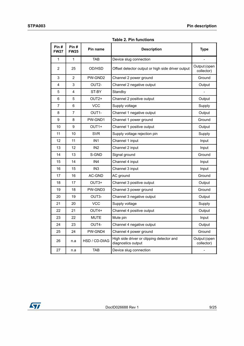
Table 2. Pin functions
Pin # FW27
Pin # FW25 Pin name Description Type
1 1 TAB Device slug connection -
2 25 OD/HSD Offset detector output or high side driver output Output (open collector)
3 2 PW-GND2 Channel 2 power ground Ground
4 3 OUT2- Channel 2 negative output Output
5 4 ST-BY Standby -
6 5 OUT2+ Channel 2 positive output Output
7 6 VCC Supply voltage Supply
8 7 OUT1- Channel 1 negative output Output
9 8 PW-GND1 Channel 1 power ground Ground
10 9 OUT1+ Channel 1 positive output Output
11 10 SVR Supply voltage rejection pin Supply
12 11 IN1 Channel 1 input Input
13 12 IN2 Channel 2 input Input
14 13 S-GND Signal ground Ground
15 14 IN4 Channel 4 input Input
16 15 IN3 Channel 3 input Input
17 16 AC-GND AC ground Ground
18 17 OUT3+ Channel 3 positive output Output
19 18 PW-GND3 Channel 3 power ground Ground
20 19 OUT3- Channel 3 negative output Output
21 20 VCC Supply voltage Supply
22 21 OUT4+ Channel 4 positive output Output
23 22 MUTE Mute pin Input
24 23 OUT4- Channel 4 negative output Output
25 24 PW-GND4 Channel 4 power ground Ground
26 n.a HSD / CD-DIAG High side driver or clipping detector and diagnostics output
Output (open collector)
27 n.a TAB Device slug connection -
Electrical specifications STPA003
10/25 DocID026688 Rev 1
3 Electrical specifications
3.1 Absolute maximum ratings
3.2 Thermal data
Table 3. Absolute maximum ratings
Symbol Parameter Value Unit
VS Operating supply voltage 18 V
VS (DC) DC supply voltage 28 V
VS (pk) Peak supply voltage (for t = 50 ms) 50 V
IOOutput peak currentNon repetitive (t = 100 μs)Repetitive (duty cycle 10 % at f = 10 Hz)
SVR Supply voltage rejection f = 100 Hz; Vr = 1 Vrms 50 70 - dB
fch High cut-off frequency PO = 0.5 W 100 300 - kHz
CT Cross talkf = 1 kHz PO = 4 Wf = 10 kHz PO = 4 W
6050
8060
--
dBdB
AM Mute attenuation POref = 4 W 80 100 - dB
Control pin characteristics
Ipin5 Standby pin current VSt-by = 0.8 V to 2.2 V - - 0.5 μA
VSB out Standby out threshold voltage (Amp: ON) 2.2 - - V
Electrical specifications STPA003
12/25 DocID026688 Rev 1
VSB in Standby in threshold voltage (Amp: OFF) - - 0.8 V
VM out Mute out threshold voltage (Amp: Play) 2.3 - - V
VM in Mute in threshold voltage (Amp: Mute) - - 0.8 V
VAM in VS automute threshold
(Amp: Mute)Att 80 dB; POref = 4 W
(Amp: Play)Att < 0.1 dB; PO = 0.5 W
4.5
-
5
-
5.5
6
V
V
Ipin23 Muting pin currentVMUTE = 0.8 V (Sourced current)
- 9 14 μA
HSD section
Vdropout Dropout voltage IO = 0.35 A - 0.25 0.3 V
Iprot Current limits - 400 - 800 mA
Offset detector
VOFF Detected differential output offset - ±2.3 ±3 ±3.7 V
VOFF_SAT Off detector saturation voltageVo > ±3 V, Ioff Det = 1 mA0 V < Voff Det < 18 V
- 0.05 0.1 V
VOFF_LK Off detector leakage current Vo < ±1 V - 0 15 μA
Clipping detector
CDLK Clip detector high leakage current Cd off - 0 1 μA
CDSAT Clip detector saturation voltage DC On; ICD = 1 mA - 0.2 0.4 V
CDTHD Clip detector THD level - - 1 - %
1. Saturated square wave output
Table 5. Electrical characteristics (continued)
Symbol Parameter Test condition Min. Typ. Max. Unit
DocID026688 Rev 1 13/25
STPA003 Electrical characteristics typical curves
24
4 Electrical characteristics typical curves
Figure 6. Quiescent current vs. supply voltage Figure 7. Output power vs. supply voltage (4 Ω)
Figure 8. Output power vs. supply voltage (2 Ω) Figure 9. Distortion vs. output power (4 Ω)
Figure 10. Distortion vs. output power (2 Ω) Figure 11. Distortion vs. frequency (4 Ω)
Electrical characteristics typical curves STPA003
14/25 DocID026688 Rev 1
Figure 12. Distortion vs. frequency (2 Ω) Figure 13. Distortion vs. output power (4 Ω, Vs = 6 V)
Figure 14. Distortion vs. output power (2 Ω, Vs = 6 V)
Figure 15. Supply voltage rejection vs. frequency
Figure 16. Crosstalk vs. frequency Figure 17. Total power dissipation & efficiency vs. Po (4 Ω, Sine)
DocID026688 Rev 1 15/25
STPA003 Electrical characteristics typical curves
24
Figure 18. Power dissipation vs. average output power (4 Ω, audio program simulation)
Figure 19. Power dissipation vs. average output power (2 Ω, audio program simulation)
Figure 20. ITU R-ARM frequency response, weighting filter for transient pop
General information STPA003
16/25 DocID026688 Rev 1
5 General information
5.1 OperationThe STPA003's inputs are ground-compatible. If the standard value for the input capacitors (0.22 μF) is adopted, the low frequency cut-off will amount to 16 Hz. For optimum pop performances, the capacitor connected to AC-GND should be four times bigger than input capacitors (see Figure 2: Standard test and application circuit (Flexiwatt25 with OD)).
Standby and mute pins are 3.3 V and 5 V compatible.
RC cells at both mute and stand-by pins have always to be used in order to smooth the transitions for preventing any audible transient noise. A time constant slower than 2.5 V/ms is suggested for the stand-by pin and 0.5 V/ms for the mute pin.
In case the standby function is not used, it could steadily be connected to Vs through a 470 kΩ resistor.
The capacitance on SVR sets the start-up and shut-down times and helps to have pop-noise free transitions. Its minimum recommended value is 10 μF. However, to have a fast start-up time, the internal resistor on SVR pin, used to set the time constant, is reduced from 100 kΩ to 3 kΩ till voltage on SVR reaches VCC/4 -2VBE and then released. In this way the capacitor on SVR is charged very quickly to VCC/4, as shown in the following figure.
Figure 21. SVR charge diagram
SVR pin accomplishes multiple functions: it is used as a reference voltage for input pins (VCC/4) the capacitor connected to SVR helps the supply voltage ripple rejection it is used as a reference to generate the half supply voltage for the output
When the amplifier goes in stand-by mode or goes out from this condition, it is suggested to put the amplifier in mute to ensure the absence of audible noise. Then the standby pin can be set to the appropriate value (ground or > 2.2 V) and the capacitance on SVR pin is discharged or charged consequently.
DocID026688 Rev 1 17/25
STPA003 General information
24
5.2 Battery variations
5.2.1 Low voltage operationMost recent OEM specifications require automatic stop for car engine at traffic lights, in order to reduce emissions of polluting substances. The STPA003, thanks to its innovating design, allows a continuous operation when battery falls down. At 6 V it is still fully operational, only the maximum output power is reduced according to the available voltage supply.
If the battery voltage drops below the minimum operating voltage of 6 V the amplifier is fast muted, the capacitor on SVR is discharged and the amplifier restarts when the battery voltage returns to the correct voltage.
5.2.2 CranksSTPA003 can sustain worst case cranks from 16 V to 6 V, continuing to play and without producing any pop noise.
Examples of battery cranking curves are shown below, indicating the shape and duration of allowed battery transitions.
t1 = 2 ms; t2 = 5 ms; t3 = 15 ms; t5 = 1 s; t6 = 50 ms
5.2.3 Advanced battery management (hybrid vehicles)In addition to compatibility with low Vbatt, the STPA003 is able to sustain upwards fast battery transitions without causing unwanted audible effects, like pop noise, and without any sound interruption thanks to the innovative circuit topology. In fact, in hybrid vehicles, the engine ignition causes a fast increase of battery voltage which can reach 16 V in less than 10 ms.
Figure 24. Upwards fast battery transitions diagram
DocID026688 Rev 1 19/25
STPA003 General information
24
5.3 Protections
5.3.1 Short circuits and open circuit operationWhen the IC detects a short circuit to ground, to Vsupply or across the load, the output of the amplifier is put in three-state (high impedance condition). The power stage remains in this condition until the short is removed.
In case of short circuit to ground or Vcc, the amplifier exits from the three-state condition only when the output returns inside the limits imposed by an internal voltage comparator.
When a short across the load is present, the power stage sees an over-current and is brought in protection mode for 100 μs. After this time, if the short circuit condition is removed the amplifier returns to play, otherwise the high impedance state is maintained and the check is repeated every 100 μs.
Disconnection of load (open load condition) doesn't damage the amplifier, which continues to play.
5.3.2 Over-voltage and load dump protectionWhen the battery voltage is higher than 19 V, the amplifier is switched to a high impedance state. It stops playing till the supply voltage returns in the permitted range.
The amplifier is protected against load dump surges having amplitude as high as 50 V and a rising time lower than 5 ms (see Figure 25).
Figure 25. Load dump protection diagram
5.3.3 Thermal protectionIf the junction temperature of the IC reaches Tj = 150 °C, a smooth mute is applied to reduce output power and limit power dissipation. If this is not enough and the junction temperature continues to increase, the amplifier is switched off when reaches the maximum temperature of 170 °C.
Figure 26. Thermal protection diagram
General information STPA003
20/25 DocID026688 Rev 1
5.4 Warnings
5.4.1 DC offset detection (OD pin)The STPA003 integrates a DC offset detector to avoid that an anomalous input DC offset is multiplied by the amplifier gain producing a dangerous large offset at the output. In fact an output offset may lead to speakers damage for overheating. To correctly detect a DC offset, the power amplifier has to be un-muted with no input signal.
When the differential output voltage is out of a window comparator with thresholds ± 3 V (typ), the OD pin is pulled down.
5.4.2 Clipping detection and diagnostics (CD-DIAG pin)When clipping occurs, the output signal is distorted. If the signal distortion on one of the output channels exceeds 1 %, the CD-DIAG pin is pulled down. This information can be sent to an audio processor in order to reduce the input signal of the amplifier and reduce the clipping.
A short to ground and short to Vcc is signaled by CD-DIAG. This pin is pulled down to 0 V till these shorts are present to inform the user a protection occurred.
CD-DIAG acts also as thermal warning. In fact every time Tj exceeds 140 °C, it is pulled down to notify this occurrence.
Figure 27. Audio section waveforms
DocID026688 Rev 1 21/25
STPA003 General information
24
5.5 Heat sink definitionAssuming we have a maximum dissipated power of 26 W (e.g. in the worst case situation of frequent clipping occurrence), considering Tj max is 150 °C and assuming ambient temperature is 70 °C, the available temperature gap for a correct dissipation is 80 °C.This means the thermal resistance of the system Rth has to be 80 °C/26 W = 3 °C/W.
The junction to case thermal resistance is 1 °C/W. So the heat sink thermal resistance should be approximately 2 °C/W. This would avoid any thermal shutdown occurrence even after long-term and full-volume operation.
Package information STPA003
22/25 DocID026688 Rev 1
6 Package information
In order to meet environmental requirements, ST offers these devices in different grades of ECOPACK® packages, depending on their level of environmental compliance. ECOPACK® specifications, grade definitions and product status are available at: www.st.com.
ECOPACK® is an ST trademark.
Figure 28. Flexiwatt25 (vertical) mechanical data and package dimensions
Figure 29. Flexiwatt27 (Vertical) mechanical data and package dimensions
Revision history STPA003
24/25 DocID026688 Rev 1
7 Revision history
Table 6. Document revision history
Date Revision Changes
11-Jul-2014 1 Initial release.
DocID026688 Rev 1 25/25
STPA003
25
Please Read Carefully:
Information in this document is provided solely in connection with ST products. STMicroelectronics NV and its subsidiaries (“ST”) reserve theright to make changes, corrections, modifications or improvements, to this document, and the products and services described herein at anytime, without notice.
All ST products are sold pursuant to ST’s terms and conditions of sale.
Purchasers are solely responsible for the choice, selection and use of the ST products and services described herein, and ST assumes noliability whatsoever relating to the choice, selection or use of the ST products and services described herein.
No license, express or implied, by estoppel or otherwise, to any intellectual property rights is granted under this document. If any part of thisdocument refers to any third party products or services it shall not be deemed a license grant by ST for the use of such third party productsor services, or any intellectual property contained therein or considered as a warranty covering the use in any manner whatsoever of suchthird party products or services or any intellectual property contained therein.
UNLESS OTHERWISE SET FORTH IN ST’S TERMS AND CONDITIONS OF SALE ST DISCLAIMS ANY EXPRESS OR IMPLIEDWARRANTY WITH RESPECT TO THE USE AND/OR SALE OF ST PRODUCTS INCLUDING WITHOUT LIMITATION IMPLIEDWARRANTIES OF MERCHANTABILITY, FITNESS FOR A PARTICULAR PURPOSE (AND THEIR EQUIVALENTS UNDER THE LAWSOF ANY JURISDICTION), OR INFRINGEMENT OF ANY PATENT, COPYRIGHT OR OTHER INTELLECTUAL PROPERTY RIGHT.
ST PRODUCTS ARE NOT DESIGNED OR AUTHORIZED FOR USE IN: (A) SAFETY CRITICAL APPLICATIONS SUCH AS LIFESUPPORTING, ACTIVE IMPLANTED DEVICES OR SYSTEMS WITH PRODUCT FUNCTIONAL SAFETY REQUIREMENTS; (B)AERONAUTIC APPLICATIONS; (C) AUTOMOTIVE APPLICATIONS OR ENVIRONMENTS, AND/OR (D) AEROSPACE APPLICATIONSOR ENVIRONMENTS. WHERE ST PRODUCTS ARE NOT DESIGNED FOR SUCH USE, THE PURCHASER SHALL USE PRODUCTS ATPURCHASER’S SOLE RISK, EVEN IF ST HAS BEEN INFORMED IN WRITING OF SUCH USAGE, UNLESS A PRODUCT ISEXPRESSLY DESIGNATED BY ST AS BEING INTENDED FOR “AUTOMOTIVE, AUTOMOTIVE SAFETY OR MEDICAL” INDUSTRYDOMAINS ACCORDING TO ST PRODUCT DESIGN SPECIFICATIONS. PRODUCTS FORMALLY ESCC, QML OR JAN QUALIFIED AREDEEMED SUITABLE FOR USE IN AEROSPACE BY THE CORRESPONDING GOVERNMENTAL AGENCY.
Resale of ST products with provisions different from the statements and/or technical features set forth in this document shall immediately voidany warranty granted by ST for the ST product or service described herein and shall not create or extend in any manner whatsoever, anyliability of ST.
ST and the ST logo are trademarks or registered trademarks of ST in various countries.Information in this document supersedes and replaces all information previously supplied.
The ST logo is a registered trademark of STMicroelectronics. All other names are the property of their respective owners.
Australia - Belgium - Brazil - Canada - China - Czech Republic - Finland - France - Germany - Hong Kong - India - Israel - Italy - Japan - Malaysia - Malta - Morocco - Philippines - Singapore - Spain - Sweden - Switzerland - United Kingdom - United States of America