40 μA Micropower Instrumentation Amplifier with Zero Crossover Distortion
AD8236
Rev. 0 Information furnished by Analog Devices is believed to be accurate and reliable. However, no responsibility is assumed by Analog Devices for its use, nor for any infringements of patents or other rights of third parties that may result from its use. Specifications subject to change without notice. No license is granted by implication or otherwise under any patent or patent rights of Analog Devices. Trademarks and registered trademarks are the property of their respective owners.
FEATURES Low power: 40 μA supply current (maximum) Low input currents
1 pA input bias current 0.5 pA input offset current
High CMRR: 110 dB CMRR, G = 100 Space-saving MSOP Zero input crossover distortion Rail-to-rail input and output Gain set with single resistor Operates from 1.8 V to 5.5 V
APPLICATIONS Medical instrumentation Low-side current sense Portable devices
CONNECTION DIAGRAM –IN 1
RG 2
RG 3
+IN 4
+VS8
VOUT7
REF6
–VS5
AD8236TOP VIEW
(Not to Scale) 0800
0-00
1
Figure 1.
1.0
2.0
4.0
3.0
5.0
0.5
1.5
3.5
2.5
4.5
0
OUTPUT VOLTAGE (V)
INPU
T C
OM
MO
N-M
OD
E VO
LTA
GE
(V)
0800
0-00
2
5.55.00.5–0.5 1.5 2.0 3.0 4.0 4.50 1.0 2.5 3.5
G = 5VS = 5VVREF = 2.5V
G = 5VS = 1.8VVREF = 0.9V
Figure 2. Wide Common-Mode Voltage Range vs. Output Voltage
GENERAL DESCRIPTION The AD8236 is the lowest power instrumentation amplifier in the industry. It has rail-to-rail outputs and can operate on voltages as low as 1.8 V. Its 40 μA maximum supply current makes it an excellent choice in battery-powered applications.
The AD8236’s high input impedance, low input bias current of 1 pA, high CMRR of 110 dB (G = 100), small size, and low power offer tremendous value. It has a wider common-mode voltage range than typical three-op-amp instrumentation amplifiers, making this a great solution for applications that operate on a single 1.8 V or 3 V supply. An innovative input stage allows for a wide rail-to-rail input voltage range without the crossover distortion common in other designs.
The AD8236 is available in an 8-lead MSOP and is specified over the industrial temperature range of −40°C to +125°C.
Table 1. Instrumentation Amplifiers by Category1 General Purpose Zero Drift
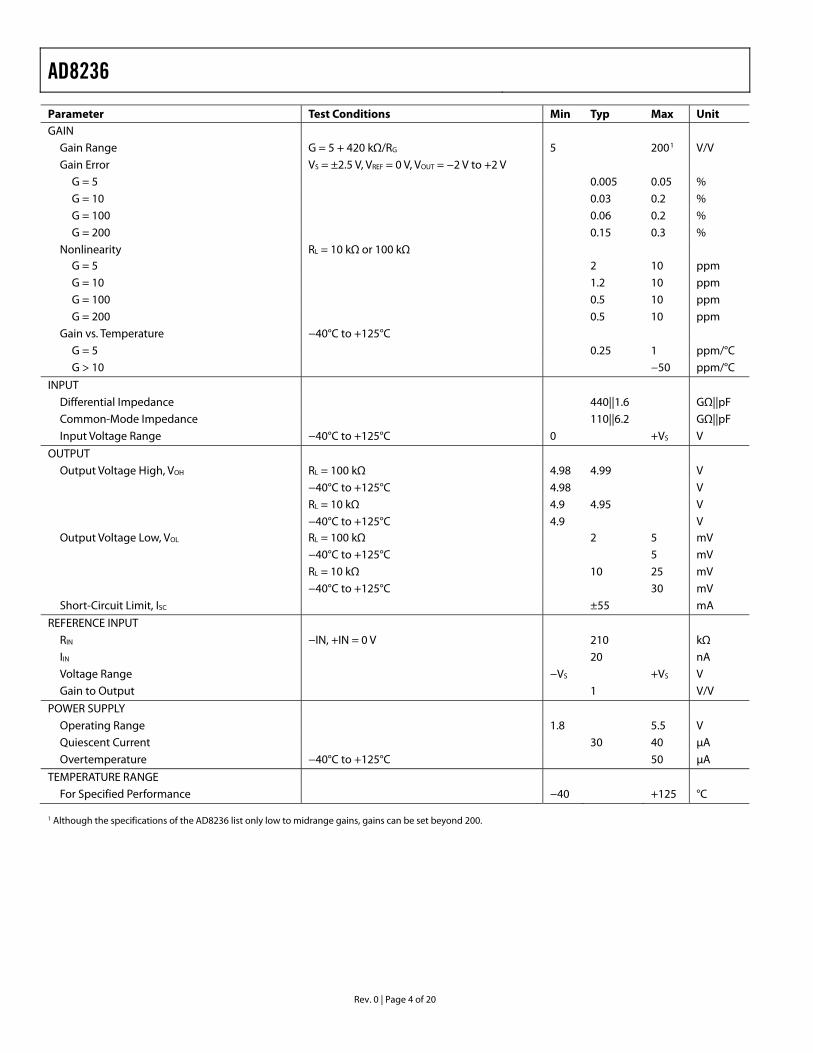
OUTPUT Output Voltage High, VOH RL = 100 kΩ 4.98 4.99 V
−40°C to +125°C 4.98 V RL = 10 kΩ 4.9 4.95 V
−40°C to +125°C 4.9 V Output Voltage Low, VOL RL = 100 kΩ 2 5 mV −40°C to +125°C 5 mV
RL = 10 kΩ 10 25 mV −40°C to +125°C 30 mV
Short-Circuit Limit, ISC ±55 mA
REFERENCE INPUT
RIN −IN, +IN = 0 V 210 kΩ IIN 20 nA
Voltage Range −VS +VS V Gain to Output 1 V/V
POWER SUPPLY
Operating Range 1.8 5.5 V Quiescent Current 30 40 μA
Overtemperature −40°C to +125°C 50 μA
TEMPERATURE RANGE For Specified Performance −40 +125 °C
1 Although the specifications of the AD8236 list only low to midrange gains, gains can be set beyond 200.
AD8236
Rev. 0 | Page 5 of 20
+VS = 1.8 V, −VS = 0 V (GND), VREF = 0.9 V, TA = 25°C, G = 5, RL = 100 kΩ to GND, unless otherwise noted.
Table 3. Parameter Test Conditions Min Typ Max Unit COMMON-MODE REJECTION RATIO (CMRR) VS = ±0.9 V, VREF = 0 V
CMRR DC VCM = −0.6 V to +0.6 V G = 5 86 94 dB
G = 10 90 100 dB G = 100 100 110 dB
G = 200 100 110 dB
NOISE Voltage Noise Spectral Density, RTI f = 1 kHz, G = 5 76 nV/√Hz
RTI, 0.1 Hz to 10 Hz G = 5 4 μV p-p G = 200 4 μV p-p
Current Noise 15 fA/√Hz VOLTAGE OFFSET
Input Offset, VOS 3.5 mV Average Temperature Coefficient (TC) −40°C to +125°C 2.5 μV/°C
Offset RTI vs. Supply (PSR) VS = 1.8 V to 5 V G = 5 100 120 dB
G = 10 110 126 dB G = 100 110 130 dB
G = 200 110 130 dB
INPUT CURRENT Input Bias Current 1 10 pA
Overtemperature −40°C to +85°C 100 pA −40°C to +125°C 600 pA Input Offset Current 0.5 5 pA Overtemperature −40°C to +85°C 50 pA −40°C to +125°C 130 pA
DYNAMIC RESPONSE
Small Signal Bandwidth, –3 dB G = 5 23 kHz G = 10 9 kHz
G = 100 0.8 kHz G = 200 0.4 kHz
Settling Time 0.01% VOUT = 1.4 V step G = 5 143 μs
G = 10 178 μs G = 100 1000 μs
G = 200 1864 μs Slew Rate
G = 5 to 100 11 mV/μs
GAIN Gain Range G = 5 + 420 kΩ/RG 5 2001 V/V
Gain Error VS = ±0.9 V, VREF = 0 V, VOUT = −0.6 V to +0.6 V G = 5 0.005 0.05 %
G = 10 0.03 0.2 % G = 100 0.06 0.2 %
G = 200 0.15 0.3 %
AD8236
Rev. 0 | Page 6 of 20
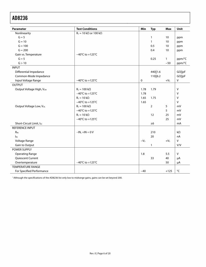
Parameter Test Conditions Min Typ Max Unit Nonlinearity RL = 10 kΩ or 100 kΩ
G = 5 1 10 ppm G = 10 1 10 ppm
G = 100 0.5 10 ppm G = 200 0.4 10 ppm
Gain vs. Temperature −40°C to +125°C G = 5 0.25 1 ppm/°C
G > 10 −50 ppm/°C
INPUT Differential Impedance 440||1.6 GΩ||pF
Common-Mode Impedance 110||6.2 GΩ||pF Input Voltage Range −40°C to +125°C 0 +VS V
OUTPUT
Output Voltage High, VOH RL = 100 kΩ 1.78 1.79 V −40°C to +125°C 1.78 V
RL = 10 kΩ 1.65 1.75 V −40°C to +125°C 1.65 V Output Voltage Low, VOL RL = 100 kΩ 2 5 mV
−40°C to +125°C 5 mV RL = 10 kΩ 12 25 mV
−40°C to +125°C 25 mV Short-Circuit Limit, ISC ±6 mA
REFERENCE INPUT RIN −IN, +IN = 0 V 210 kΩ
IIN 20 nA Voltage Range −VS +VS V
Gain to Output 1 V/V
POWER SUPPLY Operating Range 1.8 5.5 V
Quiescent Current 33 40 μA Overtemperature −40°C to +125°C 50 μA
TEMPERATURE RANGE For Specified Performance −40 +125 °C
1 Although the specifications of the AD8236 list only low to midrange gains, gains can be set beyond 200.
AD8236
Rev. 0 | Page 7 of 20
ABSOLUTE MAXIMUM RATINGS Table 4. Parameter Rating Supply Voltage 6 V Power Dissipation See Figure 3 Output Short-Circuit Current 55 mA Input Voltage (Common Mode) ±VS Differential Input Voltage ±VS Storage Temperature Range −65°C to +125°C Operating Temperature Range −40°C to +125°C Lead Temperature (Soldering, 10 sec) 300°C Junction Temperature 140°C θJA (4-Layer JEDEC Standard Board)
8-Lead MSOP 135°C/W Package Glass Transition Temperature
8-Lead MSOP 140°C ESD
Human Body Model 2 kV Charge Device Model 1 kV Machine Model 200 V
Stresses above those listed under Absolute Maximum Ratings may cause permanent damage to the device. This is a stress rating only; functional operation of the device at these or any other conditions above those indicated in the operational section of this specification is not implied. Exposure to absolute maximum rating conditions for extended periods may affect device reliability.
MAXIMUM POWER DISSIPATION The maximum safe power dissipation in the package of the AD8236 is limited by the associated rise in junction temperature (TJ) on the die. The plastic encapsulating the die locally reaches the junction temperature. At approximately 140°C, which is the glass transition temperature, the plastic changes its properties. Even temporarily exceeding this temperature limit may change the stresses that the package exerts on the die, permanently shifting the parametric performance of the AD8236.
The still-air thermal properties of the package and PCB (θJA), the ambient temperature (TA), and the total power dissipated in the package (PD) determine the junction temperature of the die. The junction temperature is calculated as
TJ = TA + (PD × θJA)
The power dissipated in the package (PD) is the sum of the quiescent power dissipation and the power dissipated in the package due to the load drive for all outputs. The quiescent power is the voltage between the supply pins (VS) times the quiescent current (IS). Assuming the load (RL) is referenced to midsupply, the total drive power is VS/2 × IOUT, some of which is dissipated in the package and some in the load (VOUT × IOUT).
The difference between the total drive power and the load power is the drive power dissipated in the package.
PD = Quiescent Power + (Total Drive Power – Load Power)
( )L
OUT
L
OUTSSSD R
VR
VVIVP
2
–2 ⎟⎟
⎠
⎞⎜⎜⎝
⎛×+×=
RMS output voltages should be considered. If RL is referenced to −VS, as in single-supply operation, the total drive power is VS × IOUT. If the rms signal levels are indeterminate, consider the worst case, when VOUT = VS/4 for RL to midsupply
( ) ( )L
SSSD R
/VIVP
24+×=
In single-supply operation with RL referenced to −VS, worst case is VOUT = VS/2.
Airflow increases heat dissipation, effectively reducing θJA. In addition, more metal directly in contact with the package leads from metal traces, through holes, ground, and power planes reduces the θJA.
Figure 3 shows the maximum safe power dissipation in the package vs. the ambient temperature for the 8-lead MSOP on a 4-layer JEDEC standard board. θJA values are approximations.
2.00
0–40 120
AMBIENT TEMPERATURE (°C)
MA
XIM
UM
PO
WER
DIS
SIPA
TIO
N (W
) 1.75
1.50
1.25
1.00
0.75
0.50
0.25
–20 0 20 40 60 80 100
0800
0-04
5
Figure 3. Maximum Power Dissipation vs. Ambient Temperature
ESD CAUTION
AD8236
Rev. 0 | Page 8 of 20
PIN CONFIGURATION AND FUNCTION DESCRIPTIONS
–IN 1
RG 2
RG 3
+IN 4
+VS8
VOUT7
REF6
–VS5
AD8236TOP VIEW
(Not to Scale)
0800
0-00
4
Figure 4. Pin Configuration
Table 5. Pin Function Descriptions Pin No. Mnemonic Description 1 −IN Negative Input Terminal (True Differential Input) 2, 3 RG Gain Setting Terminals (Place Resistor Across the RG Pins) 4 +IN Positive Input Terminal (True Differential Input) 5 −VS Negative Power Supply Terminal 6 REF Reference Voltage Terminal (Drive This Terminal with a Low Impedance Voltage Source to Level-Shift the Output) 7 VOUT Output Terminal 8 +VS Positive Power Supply Terminal
AD8236
Rev. 0 | Page 9 of 20
TYPICAL PERFORMANCE CHARACTERISTICS G = 5, +VS = 5 V, VREF = 2.5 V, RL = 100 kΩ tied to GND, TA = 25°C, unless otherwise noted.
0
CMRR (µV/V)
NU
MB
ER O
F U
NIT
S
700
600
500
400
300
200
100
–40 –20 0 20 4008
000-
060
Figure 5. Typical Distribution of CMRR, G = 5
0
VOSI (µV)
NU
MB
ER O
F U
NIT
S
800
600
400
200
–4000 –3000 –2000 –1000 0 1000 30002000 4000
0800
0-06
1
Figure 6. Typical Distribution of Input Offset Voltage
10
100
1k
1 10 100 1k 10k
NO
ISE
(nV/√H
z)
FREQUENCY (Hz)
GAIN = 5
GAIN = 200
BANDWIDTHLIMITED
0800
0-04
2
Figure 7. Voltage Noise Spectral Density vs. Frequency
1s/DIV5µV/DIV
GAIN = 5
0800
0-02
4
Figure 8. 0.1 Hz to 10 Hz RTI Voltage Noise
1s/DIV5µV/DIV
GAIN = 200
0800
0-02
5
Figure 9. 0.1 Hz to 10 Hz RTI Voltage Noise
0
20
40
60
80
100
120
140
0.1 1 10 100 1k 10k 100k
PSR
R(d
B)
FREQUNCY (Hz)
INTERNALCLIPPING
GAIN = 100GAIN = 200
GAIN = 5GAIN = 10
0800
0-03
5
Figure 10. Positive PSRR vs. Frequency, RTI, VS = ±0.9 V, ±2.5 V, VREF = 0 V
AD8236
Rev. 0 | Page 10 of 20
010.1
FREQUENCY (Hz)
PSR
R (d
B)
10 100 1k 10k 100k
120
100
80
60
40
20
0800
0-04
0
GAIN = 5
GAIN = 10
GAIN = 100
GAIN = 200
Figure 11. Negative PSRR vs. Frequency, RTI, VS = ±0.9 V, ±2.5 V, VREF = 0 V
120
01010.1 100k
FREQUENCY (Hz)
CM
RR
(dB
)
100 1k 10k
100
80
60
40
20
0800
0-02
3
GAIN = 5
GAIN = 10
GAIN = 100GAIN = 200
Figure 12. CMRR vs. Frequency, RTI
120
00.1 1 100k
FREQUENCY (Hz)
CM
RR
(dB
)
100
80
60
40
20
10 100 1k 10k
0800
0-05
1
GAIN = 5GAIN = 10
GAIN = 100GAIN = 200
Figure 13. CMRR vs. Frequency, 1 kΩ Source Imbalance, RTI
–15
–10
–5
0
5
10
15
–40 –20 0 20 40 60 80 100 120
CM
RR
(µV/
V)
TEMPERATURE (°C)
0800
0-01
4
Figure 14. Change in CMRR vs. Temperature, G = 5, Normalized at 25°C
60
–4010 1M
FREQUENCY (Hz)
GA
IN (d
B)
100 1k 10k 100k
50
40
30
20
10
0
–10
–20
–30
GAIN = 5
GAIN = 10
GAIN = 100
GAIN = 200
0800
0-02
2
Figure 15. Gain vs. Frequency, VS = 1.8 V, 5 V
0
1
2
3
4
5
6
1 10 100 1k 10k 100k
V OU
T (V
p-p
)
FREQUENCY (Hz)
0800
0-13
2
Figure 16. Maximum Output Voltage vs. Frequency
AD8236
Rev. 0 | Page 11 of 20
0800
0-02
6
0.5 1.0 1.5 2.0 2.5 3.0 3.5 4.0 4.5
NO
NLI
NEA
RIT
Y (5
ppm
/DIV
)
OUTPUT VOLTAGE (V)
VS = 5V
RLOAD = 100kΩ TIED TO GND
RLOAD = 10kΩ TIED TO GND
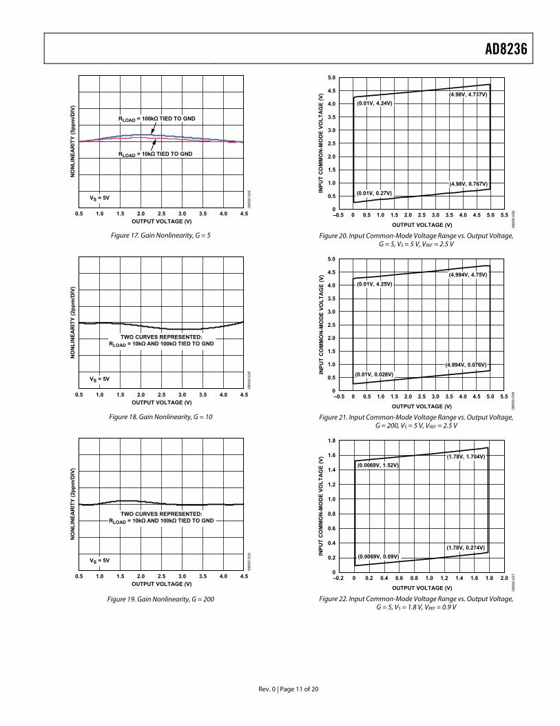
Figure 17. Gain Nonlinearity, G = 5
0800
0-02
8
0.5 1.0 1.5 2.0 2.5 3.0 3.5 4.0 4.5
NO
NLI
NEA
RIT
Y (2
ppm
/DIV
)
OUTPUT VOLTAGE (V)
VS = 5V
TWO CURVES REPRESENTED:RLOAD = 10kΩ AND 100kΩ TIED TO GND
Figure 18. Gain Nonlinearity, G = 10
0800
0-02
9
0.5 1.0 1.5 2.0 2.5 3.0 3.5 4.0 4.5
NO
NLI
NEA
RIT
Y (2
ppm
/DIV
)
OUTPUT VOLTAGE (V)
VS = 5V
TWO CURVES REPRESENTED:RLOAD = 10kΩ AND 100kΩ TIED TO GND
Figure 19. Gain Nonlinearity, G = 200
0 0.5 2.01.51.0 2.5 3.0 3.5 4.0 4.5 5.0
5.0
0
0.5
–0.5 5.5
OUTPUT VOLTAGE (V)
INPU
T C
OM
MO
N-M
OD
E VO
LTA
GE
(V)
4.0
4.5
3.0
3.5
2.5
1.5
2.0
1.0
0800
0-03
6
(0.01V, 4.24V)(4.98V, 4.737V)
(0.01V, 0.27V)(4.98V, 0.767V)
Figure 20. Input Common-Mode Voltage Range vs. Output Voltage, G = 5, VS = 5 V, VREF = 2.5 V
0 0.5 1.0 1.5 2.0 2.5 3.0 3.5 4.0 4.5 5.0
5.0
4.5
0–0.5 5.5
OUTPUT VOLTAGE (V)
INPU
T C
OM
MO
N-M
OD
E VO
LTA
GE
(V)
4.0
3.5
3.0
2.5
2.0
1.5
1.0
0.5
0800
0-03
8
(0.01V, 4.25V)
(0.01V, 0.026V)
(4.994V, 4.75V)
(4.994V, 0.076V)
Figure 21. Input Common-Mode Voltage Range vs. Output Voltage, G = 200, VS = 5 V, VREF = 2.5 V
0 0.2 0.80.60.4 1.0 1.2 1.4 1.6 1.8
1.8
0
0.2
–0.2 2.0
OUTPUT VOLTAGE (V)
INPU
T C
OM
MO
N-M
OD
E VO
LTA
GE
(V) 1.6
1.2
1.4
1.0
0.6
0.8
0.4
0800
0-03
7
(0.0069V, 1.52V)(1.78V, 1.704V)
(1.78V, 0.274V)(0.0069V, 0.09V)
Figure 22. Input Common-Mode Voltage Range vs. Output Voltage, G = 5, VS = 1.8 V, VREF = 0.9 V
AD8236
Rev. 0 | Page 12 of 20
0 0.2 0.80.60.4 1.0 1.2 1.4 1.6 1.8
1.8
0
0.2
–0.2 2.0
OUTPUT VOLTAGE (V)
INPU
T C
OM
MO
N-M
OD
E VO
LTA
GE
(V) 1.6
1.2
1.4
1.0
0.6
0.8
0.4
0800
0-03
9
(0.03V, 1.533V)
(0.03V, 0.103V)(1.75V, 0.275V)
(1.75V, 1.705V)
Figure 23. Input Common-Mode Voltage Range vs. Output Voltage, G = 200, VS = 1.8 V, VREF = 0.9 V
+VS
–VS1.8
SUPPLY VOLTAGE (V)
OU
TPU
T VO
LTA
GE
SWIN
G (V
)R
EFER
RED
TO
SU
PPLY
VO
LTA
GE
–0.001
–0.002
–0.003
+0.002
+0.003
+0.001
2.3 2.8 3.3 3.8 4.3 4.8
0800
0-05
4
–40°C+25°C+85°C+125°C
–40°C+25°C+85°C+125°C
Figure 24. Output Voltage Swing vs. Supply Voltage, VS = ±0.9 V, ±2.5 V, VREF = 0 V, RL = 100 kΩ Tied to −VS
+VS
–VS1k 100k
0357
9-05
6
RLOAD (Ω)
OU
TPU
T VO
LTA
GE
SWIN
G (V
)R
EFER
RED
TO
SU
PPLY
VO
LTA
GE
10k
–0.1
+0.001
+0.002
+0.003
–0.2
–0.3
+25°C+85°C+125°C
–40°C
+125°C
+25°C+85°C
–40°C
Figure 25. Output Voltage Swing vs. Load Resistance, VS = ±0.9 V, ±2.5 V, VREF = 0 V, RL = 100 kΩ Tied to −VS
1ms/DIV
2V/D
IV
444μs TO 0.01%
0800
0-04
7
Figure 26. Large Signal Pulse Response and Settling Time, VS = ±2.5 V, VREF = 0 V, RL = 10 kΩ to VREF
1ms/DIV
700m
V/D
IV
143.2μs TO 0.01%
0800
0-04
8
Figure 27. Large Signal Pulse Response and Settling Time, VS = ±0.9 V, VREF = 0 V, RL = 10 kΩ to VREF
0800
0-11
7
100µs/DIV
20m
V/D
IV
Figure 28. Small Signal Pulse Response, G = 5, VS = ±2.5 V, VREF = 0 V, RL = 100 kΩ to VREF, CL = 100 pF
AD8236
Rev. 0 | Page 13 of 20
0800
0-01
7
100µs/DIV
20m
V/D
IV
Figure 29. Small Signal Pulse Response, G = 5, CL = 100 pF, VS = ±0.9 V, VREF = 0 V, RL = 100 kΩ to VREF
0800
0-11
3
1ms/DIV
20m
V/D
IV
Figure 30. Small Signal Pulse Response, G = 200, CL = 100 pF, VS = 2.5 V, VREF = 0 V, RL = 100 kΩ to VREF
0800
0-01
3
20m
V/D
IV
1ms/DIV
Figure 31. Small Signal Pulse Response, G = 200, CL = 100 pF, VS = 0.9 V, VREF = 0 V, RL = 100 kΩ to VREF
500
00 4
OUTPUT VOLTAGE STEP SIZE (V)
SETT
LIN
G T
IME
(µs)
400
200
300
100
1 2 3
0800
0-04
3
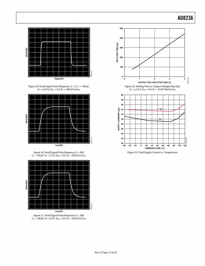
Figure 32. Settling Time vs. Output Voltage Step Size, VS = ±2.5 V, VREF = 0 V, RL = 10 kΩ Tied to VREF
20
22
24
26
28
30
32
34
36
38
40
–40 –25 –10 5 20 35 50 65 80 95 110 125
SUPP
LYC
UR
REN
T(µ
A)
TEMPERATURE (°C)
1.8V
5V
0800
0-03
4
Figure 33. Total Supply Current vs. Temperature
AD8236
Rev. 0 | Page 14 of 20
THEORY OF OPERATION
0800
0-00
6
RGRGRG
REF
–IN +IN
VOUT
210kΩ 210kΩ52.5kΩ 52.5kΩ
AD8236
2 3
+VS8
–VS5
1 4
7
6
ESDPROTECTION
ESDPROTECTION
ESDPROTECTION
ESDPROTECTION
ESDPROTECTION
ESDPROTECTION
OP AMPA OP AMP
B
Figure 34. Simplified Schematic
The AD8236 is a monolithic, 2-op-amp instrumentation amplifier. It was designed for low power, portable applications where size and low quiescent current are paramount. For example, it has a rail-to-rail input and output stage to offer more dynamic range when operating on low voltage batteries. Unlike traditional rail-to-rail input amplifiers that use a complementary differential pair stage and suffer from nonlinearity, the AD8236 uses a novel architecture to internally boost the supply rail, allowing the amplifier to operate rail to rail yet still deliver a low 0.5 ppm of nonlinearity. In addition, the 2-op-amp instrumentation amplifier architecture offers a wide operational common-mode voltage range. Additional information is provided in the Common-Mode Input Voltage Range section. Precision, laser-trimmed resistors provide the AD8236 with a high CMRR of 86 dB (minimum) at G = 5 and gain accuracy of 0.05% (maximum).
BASIC OPERATION The AD8236 amplifies the difference between its positive input (+IN) and its negative input (−IN). The REF pin allows the user to level-shift the output signal. This is convenient when interfacing to a filter or analog-to-digital converter (ADC). The basic setup is shown in Figure 35. Figure 37 shows an example configuration for operating the AD8236 with dual supplies. The equation for the AD8236 is as follows:
VOUT = G × (VINP − VINM) + VREF
If no gain setting resistor is installed, the default gain, G, is 5. The Gain Selection section describes how to program the gain, G.
AD8236RG
+IN+VS
5V
0.1µF
–VS
VINP
GAIN SETTINGRESISTOR
VINM
OUT
REF
VREF
VOUTRG
–IN
0800
0-13
6
Figure 35. Basic Setup
GAIN SELECTION Placing a resistor across the RG terminals sets the gain of the AD8236, which can be calculated by referring to Table 6 or by using the gain equation
5kΩ420−
=G
RG
Table 6. Gains Achieved Using 1% Resistors 1% Standard Table Value of RG (Ω) Calculated Gain 422 k 6.0 210 k 7.0 140 k 8.0 105 k 9.0 84.5 k 10.0 28 k 20.0 9.31 k 50.1 4.42 k 100.0 2.15 k 200.3
The AD8236 defaults to G = 5 when no gain resistor is used. Gain accuracy is determined by the absolute tolerance of RG. The TC of the external gain resistor increases the gain drift of the instrumentation amplifier. Gain error and gain drift are at a minimum when the gain resistor is not used.
AD8236
Rev. 0 | Page 15 of 20
INCORRECTLAYOUT Careful board layout maximizes system performance. In applications that need to take advantage of the low input bias current of the AD8236, avoid placing metal under the input path to minimize leakage current.
Grounding
The output voltage of the AD8236 is developed with respect to the potential on the reference terminal, REF. To ensure the most accurate output, the trace from the REF pin should either be connected to the AD8236 local ground (see Figure 37) or connected to a voltage that is referenced to the AD8236 local ground (Figure 35).
REFERENCE TERMINAL The reference terminal, REF, is at one end of a 210 kΩ resistor (see Figure 34). The output of the instrumentation amplifier is referenced to the voltage on the REF terminal; this is useful when the output signal needs to be offset to voltages other than common. For example, a voltage source can be tied to the REF pin to level-shift the output so that the AD8236 can interface with an ADC. The allowable reference voltage range is a function of the gain, common-mode input, and supply voltages. The REF pin should not exceed either +VS or −VS by more than 0.5 V.
For best performance, especially in cases where the output is not measured with respect to the REF terminal, source impedance to the REF terminal should be kept low because parasitic resistance can adversely affect CMRR and gain accuracy. Figure 36 demonstrates how an op amp is configured to provide a low source impedance to the REF terminal when a midscale reference voltage is desired.
V
CORRECT
AD8236REF
AD8236
OP AMP+
–
V
0800
0-13
7
REF
Figure 36. Driving the REF Pin
POWER SUPPLY REGULATION AND BYPASSING The AD8236 has high power supply rejection ration (PSRR). However, for optimal performance, a stable dc voltage should be used to power the instrumentation amplifier. Noise on the supply pins can adversely affect performance. As in all linear circuits, bypass capacitors must be used to decouple the amplifier.
A 0.1 μF capacitor should be placed close to each supply pin. A 10 μF tantalum capacitor can be used further away from the part (see Figure 37). In most cases, it can be shared by other precision integrated circuits.
AD8236
+VS
+IN
–INLOAD
REF
0.1µF 10µF
0.1µF 10µF
–VS
VOUT
0800
0-13
8
Figure 37. Supply Decoupling, REF, and Output Referred to Ground
AD8236
Rev. 0 | Page 16 of 20
R
R
1fHIGH-PASS = 2πRC
TRANSFORMER
AC-COUPLED
REF
C
–VS
+VS
AD8236
REF
–VS
+VS
AD8236
TRANSFORMER
AC-COUPLED
REF
C
–VS
+VS
AD8236
REF
–VS
+VS
AD8236
0800
0-13
9
Figure 38. Creating an IBIAS Path
INPUT BIAS CURRENT RETURN PATH The AD8236 input bias current is extremely small at less than 10 pA. Nonetheless, the input bias current must have a return path to common. When the source, such as a transformer, cannot provide a return current path, one should be created (see Figure 38).
INPUT PROTECTION All terminals of the AD8236 are protected against ESD. In addition, the input structure allows for dc overload conditions a diode drop above the positive supply and a diode drop below the negative supply. Voltages beyond a diode drop of the supplies cause the ESD diodes to conduct and enable current to flow through the diode. Therefore, an external resistor should be used in series with each of the inputs to limit current for voltages above +VS. In either scenario, the AD8236 safely handles a continuous 6 mA current at room temperature.
For applications where the AD8236 encounters extreme overload voltages, as in cardiac defibrillators, external series resistors and low leakage diode clamps, such as BAV199Ls, FJH1100s, or SP720s, should be used.
RF INTERFERENCE RF rectification is often a problem in applications where there are large RF signals. The problem appears as a small dc offset voltage. The AD8236, by its nature, has a 3.1 pF gate capacitance, CG, at each input. Matched series resistors form a natural low-pass filter that reduces rectification at high frequency (see Figure 39). The relationship between external, matched series resistors and the internal gate capacitance is expressed as
GDIFF RC
FilterFreqπ2
1=
GCM RC
FilterFreqπ2
1=
AD8236VOUT
REF
–VS
CG
CG
–VS
+VS
–VS
R
R
+IN
–IN
0.1µF 10µF
0.1µF 10µF
0800
0-14
0
Figure 39. RFI Filtering Without External Capacitors
AD8236
Rev. 0 | Page 17 of 20
To eliminate high frequency common-mode signals while using smaller source resistors, a low-pass RC network can be placed at the input of the instrumentation amplifier (see Figure 40). The filter limits the input signal bandwidth according to the following relationship:
)2(π21
GCDDIFF CCCR
FilterFreq++
=
)(π21
GCCM CCR
FilterFreq+
=
Mismatched CC capacitors result in mismatched low-pass filters. The imbalance causes the AD8236 to treat what would have been a common-mode signal as a differential signal. To reduce the effect of mismatched external CC capacitors, select a value of CD greater than 10 times CC. This sets the differential filter frequency lower than the common-mode frequency.
R
R
AD8236
+VS
–IN
+IN
10µF0.1µF
VOUT
REF
CC
CC
CD
1nF
1nF
10nF
4.02kΩ
4.02kΩ
0800
0-14
1
Figure 40. RFI Suppression
COMMON-MODE INPUT VOLTAGE RANGE The common-mode input voltage range is a function of the input voltages, reference voltage, supplies, and the output of Internal Op Amp A. Figure 34 shows the internal nodes of the AD8236. Figure 20 to Figure 23 show the common-mode voltage ranges for typical supply voltages and gains.
If the supply voltages and reference voltage is not represented in Figure 20 to Figure 23, the following methodology can be used to calculate the acceptable common-mode voltage range:
1. Adhere to the input, output, and reference voltage ranges shown in Table 2 and Table 3.
2. Calculate the output of the internal op amp, A. The following equation calculates this output:
4RkΩ52.5
245
G
REFDIFF
DIFFCM
VVVVA −−⎟
⎠⎞
⎜⎝⎛ −=
where: VDIFF is defined as the difference in input voltages, VDIFF = VINP − VINM. VCM is defined as the common mode voltage, VCM = (VINP + VINM)/2.
If no gain setting resistor, RG, is installed, set RG to infinity.
3. Keep A within 10 mV of either supply rail. This is valid over the −40°C to +125°C temperature range.
−VS + 10 mV < A < +VS – 10 mV
AD8236
Rev. 0 | Page 18 of 20
APPLICATIONS INFORMATION AC-COUPLED INSTRUMENTATION AMPLIFIER An integrator can be tied to the AD8236 in feedback to create a high-pass filter as shown in Figure 41. This circuit can be used to reject dc voltages and offsets. At low frequencies, the impedance of the capacitor, C, is high. Therefore, the gain of the integrator is high. DC voltage at the output of the AD8236 is inverted and gained by the integrator. The inverted signal is injected back into the REF pin, nulling the output. In contrast, at high frequencies, the integrator has low gain because the impedance of C is low. Voltage changes at high frequencies are inverted but at a low gain. The signal is injected into the REF pins, but it is not enough to null the output. At very high frequencies, the capacitor appears as a short. The op amp is at unity gain. High frequency signals are, therefore, allowed to pass.
When a signal exceeds fHIGH-PASS, the AD8236 outputs the high-pass filtered input signal.
AD8236
AD8603
R
+VS
+IN
–IN
0.1µF
0.1µF
10µF
REFC
+VS
+VS
VREF
12πRCfHIGH-PASS =
0800
0-14
2
Figure 41. AC-Coupled Circuit
AD8236
Rev. 0 | Page 19 of 20
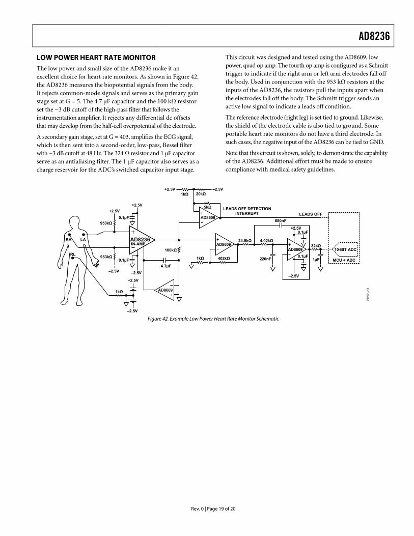
LOW POWER HEART RATE MONITOR The low power and small size of the AD8236 make it an excellent choice for heart rate monitors. As shown in Figure 42, the AD8236 measures the biopotential signals from the body. It rejects common-mode signals and serves as the primary gain stage set at G = 5. The 4.7 μF capacitor and the 100 kΩ resistor set the −3 dB cutoff of the high-pass filter that follows the instrumentation amplifier. It rejects any differential dc offsets that may develop from the half-cell overpotential of the electrode.
A secondary gain stage, set at G = 403, amplifies the ECG signal, which is then sent into a second-order, low-pass, Bessel filter with −3 dB cutoff at 48 Hz. The 324 Ω resistor and 1 μF capacitor serve as an antialiasing filter. The 1 μF capacitor also serves as a charge reservoir for the ADC’s switched capacitor input stage.
This circuit was designed and tested using the AD8609, low power, quad op amp. The fourth op amp is configured as a Schmitt trigger to indicate if the right arm or left arm electrodes fall off the body. Used in conjunction with the 953 kΩ resistors at the inputs of the AD8236, the resistors pull the inputs apart when the electrodes fall off the body. The Schmitt trigger sends an active low signal to indicate a leads off condition.
The reference electrode (right leg) is set tied to ground. Likewise, the shield of the electrode cable is also tied to ground. Some portable heart rate monitors do not have a third electrode. In such cases, the negative input of the AD8236 can be tied to GND.
Note that this circuit is shown, solely, to demonstrate the capability of the AD8236. Additional effort must be made to ensure compliance with medical safety guidelines.
+2.5V+2.5V
–2.5V
+2.5V
–2.5V
–2.5V–2.5V
0.1µF
0.1µF
0.1µF+2.5V
AD8609
AD8236IN-AMP AD8609
AD8609
AD8609
+2.5V –2.5V
LEADS OFF DETECTIONINTERRUPT LEADS OFF
402kΩ1kΩ
1kΩ
24.9kΩ324Ω
1µF220nF
4.7µF
100kΩ
953kΩ
RA LA
RL 953kΩ
1kΩ 20kΩ
5kΩ
680nF
4.02kΩ
MCU + ADC
10-BIT ADC
0800
0-14
3
0.1µF
Figure 42. Example Low Power Heart Rate Monitor Schematic