19
450mm and Moore’s Law Advanced Packaging Challenges and the Impact of 3D Doug Anberg Doug Anberg VP, Technical Marketing Ultratech SOKUDO Lithography Breakfast Forum July 10, 2013

450mm and Moore’s Law
Advanced Packaging Challenges and the Impact of 3D
Doug AnbergDoug Anberg
VP, Technical Marketing
Ultratech
SOKUDO Lithography Breakfast Forum
July 10, 2013

Agenda
• Next Generation Technology Cost Impact to Moore’s Law
• Innovation vs. Scaling
• Emerging 3D Advanced Packaging Applications
••Technical Challenges for 450mm Advanced Packaging Lithography
• Summary

0.0636
0.0521
0.06
0.07
Cost per Million Gates ($)
2,500
2,000
Cost of Developing Next-Generation Process Technologies
Cost per Gate by Process Node
Accelerating Costs• Cost of developing Next-Gen technologies is accelerating•While historic “Cost-per-Gate” reduction trend has stopped
0.0521
0.0362
0.02670.0275 0.0278
0.00
0.01
0.02
0.03
0.04
0.05
90nm 65nm 40nm 28nm 20nm 14nm
Cost per Million Gates ($)
Source: EE Times
Cost (M$)
1,500
1,000
500
065nm 45nm 32/28nm 20nm 14nm130nm180nm 90nm
Source: IBS

50
60
70
80
Estimated Number of Manageable Designs in First 12 Months of Process Being Ready for Production (Each Foundry)
65 - 75
Declining Designs
Source: IBS
0
10
20
30
40
50
65nm 40nm 28nm 20nm 14nm
5 - 8
40 - 50
20 - 30
10 - 20

No Cost-effective Lithography Solutions
• High cost and availability of production EUV• Integration of EUV and FinFET technology on 450mm wafers• Expected to drive 3D integration to have major impact on extending Moore’s law
Source: IBM, 2013

Next Generation Technology Node Gains Coming From Innovation
• 3D and other technology innovations are now driving device improvement significantly more than gate scaling
Source: IBM, 2013

Innovation Includes New Advanced Packaging Solutions and Challenges

•• TSV improves system level performance without
further transistor shrink
• Initial TSV adoption for
Emerging 3D Advanced Packaging Applications
TSV For CMOS Image Sensor
TSV For Leading Edge Devices
Source: Tech Search International
• Initial TSV adoption for cell phone camera
modules
• High performance logic will adapt TSV solutions
for bandwidth
performance in the future

3D TSV Technology Roadmap (IMEC)
FIB-cross section of stacked CMOS test chips with 5µµµµm diameter Cu TSV at 10µµµµm pitch
• 3D integration enables a higher integration density• Using 3D chip stacking can extend the number of functions per 3D chip well beyond the near-term capabilities of traditional scaling, helping extend
Moore’s lawSource: IMEC 3D System Integration Fact Sheet
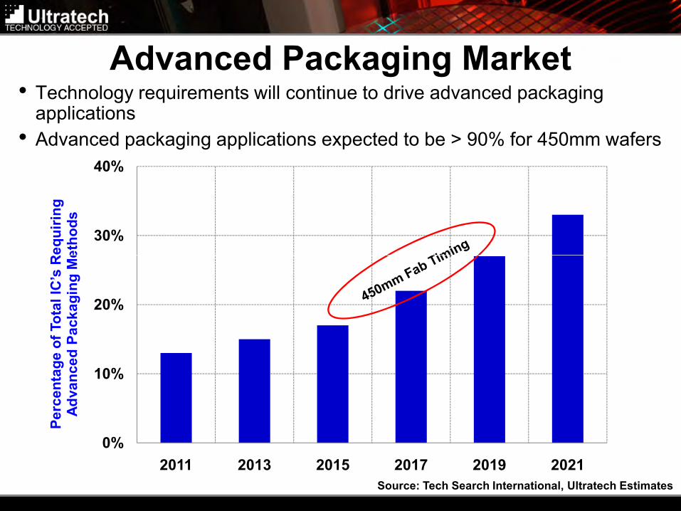
30%
40%
IC’s Requiring
Advanced Packaging Methods
Advanced Packaging Market• Technology requirements will continue to drive advanced packaging applications
• Advanced packaging applications expected to be > 90% for 450mm wafers
Source: Tech Search International, Ultratech Estimates
0%
10%
20%
2011 2013 2015 2017 2019 2021
Percentage of Total IC’s Requiring
Advanced Packaging Methods

Technical Challenges for 450mm Advanced Packaging
• Developing advanced TSV solutions for 3D• Through-silicon (Dual Side) alignment for 450mm wafers
• In-situ metrology for Dual Side alignment
• Scaling warped wafer handling solutions• 450mm wafers will have up to 2mm of warpage at final BEOL • 450mm wafers will have up to 2mm of warpage at final BEOL lithography levels
• Scaling edge processing solutions• Both wafer edge protection and wafer edge exposure solutions are required and must not significantly impact productivity
• Maintaining low CoO with thick resists, high exposure dose processes• Resist processes in excess of 100um thick requiring exposure doses in excess of 1000mJ/cm2 will need to be accommodated with high throughput

Ultratech Advanced Packaging Lithography Solutions for 450mm
•Ultratech’s 450mm Advanced Packaging stepper is based on a
production proven 300mm
modular platform designed for
scalability
•High power illumination systems •High power illumination systems and advanced 1X projection
optics designs provide equivalent
300mm throughput on a per wafer
basis
•Options available to support the unique requirements of through
silicon via, extremely warped
wafers and thick resist processing
Unity Modular Design Enables Low-Risk Scalability to 450mm
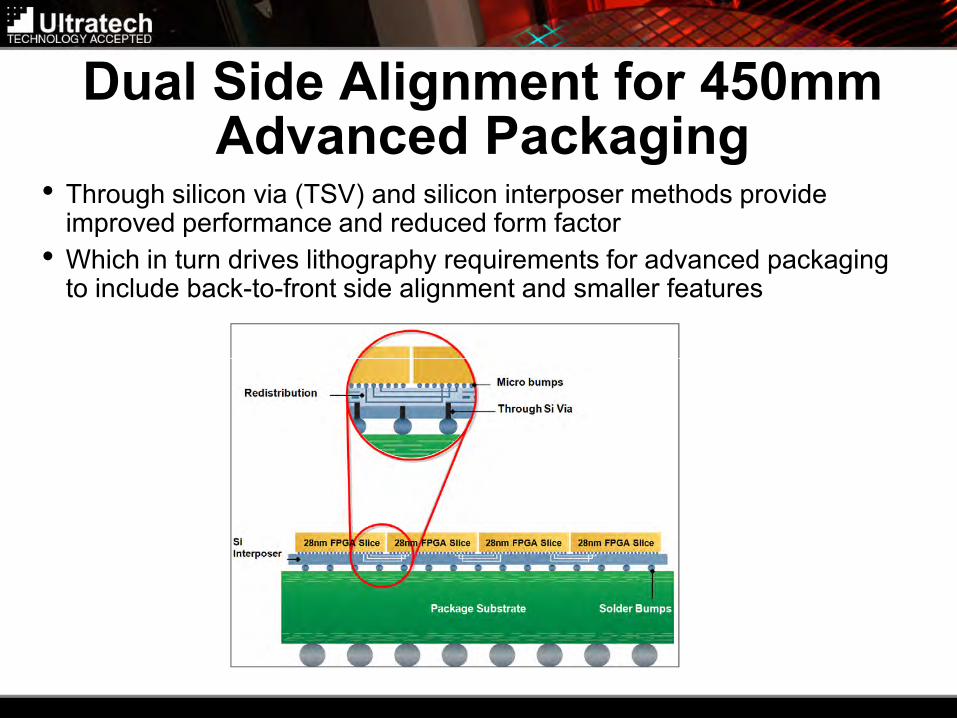
Dual Side Alignment for 450mm Advanced Packaging
• Through silicon via (TSV) and silicon interposer methods provide improved performance and reduced form factor
• Which in turn drives lithography requirements for advanced packaging to include back-to-front side alignment and smaller features

Through Silicon Via (TSV) Fabrication
Lithography for through silicon via
Device wafer Thinned silicon, bonded to carrier silicon viacarrier
•Challenges for TSV lithography• How to precisely align to device features embedded below silicon?
• How to measure performance?

TSV Alignment and In-Situ Metrology Using Top IR Source
silicon
camera
photoresist
Z offset
Alignment system
camera
photoresist• Top directed IR illumination allows for flexible placement of
Front side metrology
silicon
carrier
Back side metrology
silicon
carrier
flexible placement of targets on the wafer
• Stepper-Self-Metrology measures XY positions of two features at different Z heights
200 micron thick silicon

Microbumps for 450mm Advanced Packaging
• Microbumps are used for 3D die-to-die and die-to-wafer stacking and interposer applications
• Aggressive scaling of microbump sizes and pitch are essential to meet next generation and 450mm interconnect requirements
3.5µµµµm microbump with 10.0µµµµm pitch3D-stacked test die with CuSn µµµµbump connections
(IMEC)

Experimental Microbump Results
• 3.5µm CD with 10.0µm pitch, resist thickness 13.2µm• Process requirements are bottom CD of 3.5 µm ± 10% andsidewall angle > 87 degrees
Process Window Microbump Cross Section
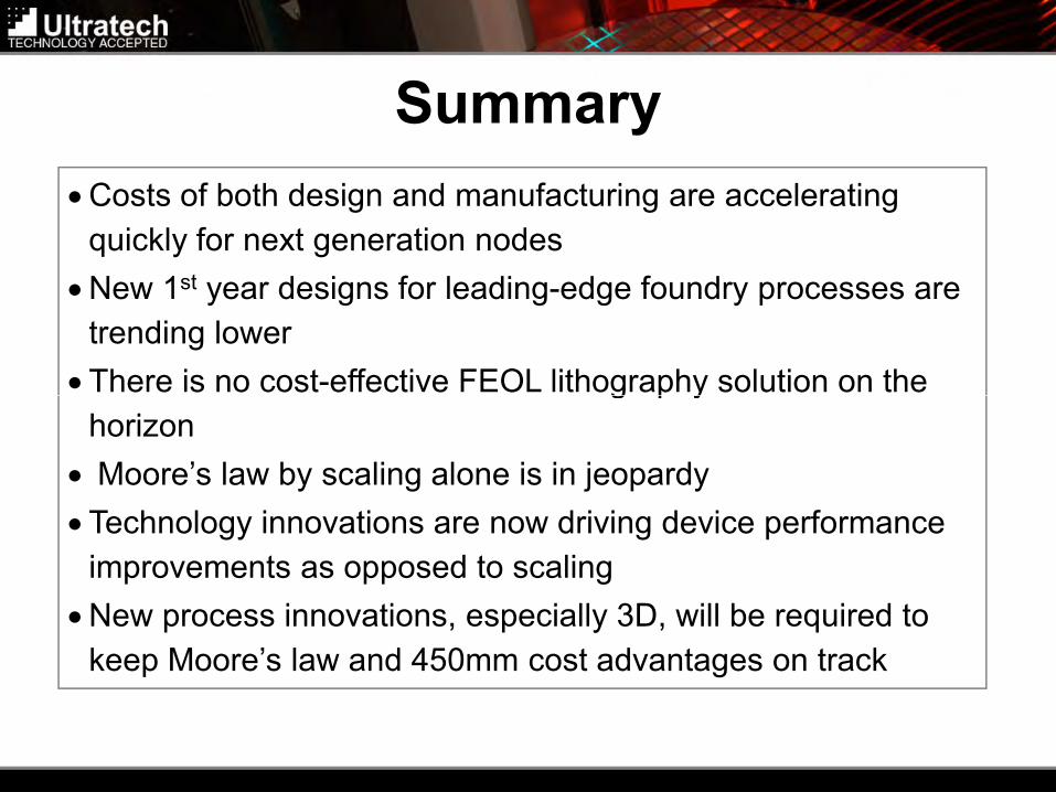
Summary
•Costs of both design and manufacturing are accelerating
quickly for next generation nodes
•New 1st year designs for leading-edge foundry processes are
trending lower
•There is no cost-effective FEOL lithography solution on the •There is no cost-effective FEOL lithography solution on the
horizon
• Moore’s law by scaling alone is in jeopardy
•Technology innovations are now driving device performance
improvements as opposed to scaling
•New process innovations, especially 3D, will be required to
keep Moore’s law and 450mm cost advantages on track


