© 2006 Cisco Systems, Inc. All rights reserved. Cisco ConfidentialPresentation_ID 1
45nm SemiconductorTechnology and Reliability Challenges
ShiJie Wen – Cisco Component EngineeringJune 2008
© 2006 Cisco Systems, Inc. All rights reserved. Cisco ConfidentialPresentation_ID 2
• 45nm Si Technology Overview
• Quality/Reliability Challenges•Si Technology•Package Technology
Outline
© 2006 Cisco Systems, Inc. All rights reserved. Cisco ConfidentialPresentation_ID 3
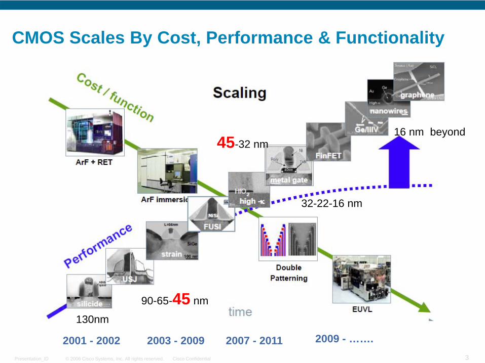
CMOS Scales By Cost, Performance & Functionality
130nm
90-65-45 nm
45-32 nm
32-22-16 nm
16 nm beyond
2001 - 2002 2003 - 2009 2009 - …….2007 - 2011
© 2006 Cisco Systems, Inc. All rights reserved. Cisco ConfidentialPresentation_ID 4
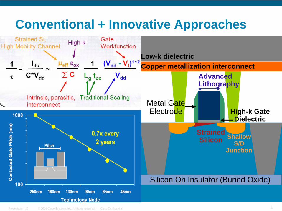
Conventional + Innovative Approaches
Copper metallization interconnectLow-k dielectric
Silicon On Insulator (Buried Oxide)
Strained Silicon Shallow
S/D Junction
Advanced Lithography
High-k Gate Dielectric
Metal Gate Electrode
© 2006 Cisco Systems, Inc. All rights reserved. Cisco ConfidentialPresentation_ID 5
Advanced Lithography - ImmersionAdvantage1. Immersion lithography provides
enhanced resolution and
expanded depth of focus (DOF).
Critical layers are Poly, M1 & Cont
Disadvantage1. Cost and experience
2. New Photo Resist compatible with immersion liquid
3. Productivity or through put of immersion is lower than Dry
4. New defects caused by micro-air-bubbles, water mark, particles, etc. are unique to immersion lithography.
Technology A B C D E
65nm Dry Dry Dry Dry Dry
45nm Wet Wet Wet Wet Dry
© 2006 Cisco Systems, Inc. All rights reserved. Cisco ConfidentialPresentation_ID 6
High-K Gate DielectricsSiO2 gate scaling limited to ~12A because of high Ig & reliability.
SiON or Nitrided SiO2, has a higher K dielectric value.
1. Lower EOT (Equivalent Oxide Thickness) means better control of short channel effects and higher current drive.
2. Enable thicker Tox for less Ig & better breakdown strength.
HfO2 films have higher K than SiON
1. Pros: Even lower EOT for higher
performance and lower Ig
2. Con: New Material – unknown
reliability, manufacture learning
Technology A B C D E65nm SiON SiON SiON SiON SiON45nm SiON SiON SiON SiON HfO2
© 2006 Cisco Systems, Inc. All rights reserved. Cisco ConfidentialPresentation_ID 7
Metal Gate ElectrodesAdvantage:
1. Metal gate with high K -> thinner Tox.• Better short channel control• Reduces leakage current • increases driving current
2. Poly gate resistivity gets too high and does not work well with higher K .
Disadvantage:
1. Long term reliability data, Wafer Level Reliability, are limited at this time.
2. Only 1 vendor committed in 45nm & no detail information is available.
3. Thermal stabilities issues: Vt voltage shifts & re-growth in the gate stack.
4. Work-function of metal adds complexity to generate low Vt for both P & N
Technology A B C D E65nm Poly Poly Poly Poly Poly45nm Poly Poly Poly Poly Dual Metal
© 2006 Cisco Systems, Inc. All rights reserved. Cisco ConfidentialPresentation_ID 8
Strained SiliconStrained silicon is used to increase transistor current:1. N-channel: Tensile Strain increase electron mobility
1. Tensile Stress liner2. Tensile Stress Memorization
2. P-channel: Compressive Strain increase hole mobility1. Compressive Stress liner, PMD2. SiGe – embedded S/D3. Lattice Orientation
. Strained effects are
additive, 45nm processes
combine more strained
silicon features
SiGe in S/D is new experience
© 2006 Cisco Systems, Inc. All rights reserved. Cisco ConfidentialPresentation_ID 9
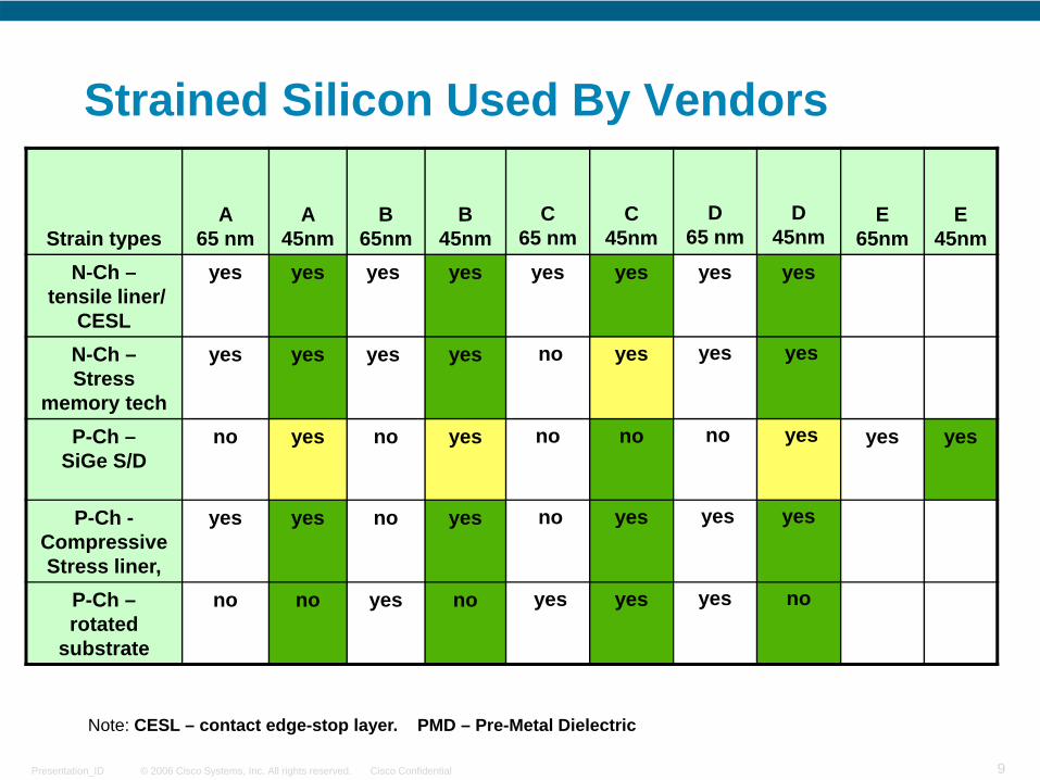
Strained Silicon Used By Vendors
Strain typesA
65 nmA
45nmB
65nmB
45nmC
65 nmC
45nmD
65 nmD
45nmE
65nmE
45nmN-Ch –
tensile liner/ CESL
yes yes yes yes yes yes yes yes
N-Ch –Stress
memory tech
yes yes yes yes no yes yes yes
P-Ch –SiGe S/D
no yes no yes no no no yes yes yes
P-Ch -Compressive Stress liner,
yes yes no yes no yes yes yes
P-Ch –rotated
substrate
no no yes no yes yes yes no
Note: CESL – contact edge-stop layer. PMD – Pre-Metal Dielectric
© 2006 Cisco Systems, Inc. All rights reserved. Cisco ConfidentialPresentation_ID 10
SOI – Silicon On InsulatorAdvantage vs. bulk
1. Higher performance
2. Lower Power – less
sub-threshold leakage
3. No latch-up, 5X better SER
Disadvantage
1. Floating body history effect -
more timing variations, SRAM design, pulse degeneration etc.
2. Local self-heating effect because buried oxide layer thermal resistivity is about 100x of silicon.
3. Learning curve on SOI ASIC designTechnology A B C D E
0.25u to 65nm CPU No No No No45nm ASIC & CPU No No No No
32nm ASIC & CPU May be Yes ? No
TR.OX
C
D
GATE
BURIED OXIDE
Si SUBSTRATE
BURIED OXIDE
TR.OX
SOURCE DRAIN
C1 C1
Si P+ TR.OXN+ N+
SOI
© 2006 Cisco Systems, Inc. All rights reserved. Cisco ConfidentialPresentation_ID 11
Ultra Shallow Junction, Source/Drain
Technology A B C D E65nm RTA RTA RTA ? ?45nm LSA ? LSA ? LSA
To increase transistor Current -> Decrease resistance in Contact, Junction and Extension -> Higher S/D implant Doses and Higher Anneal Temp
To reduce leakage current -> Reduce Junction Depth -> Lower Implant Energies, Shorter Anneal Time
Solutions – New equipment and implant process
1. Laser Spike Annealing, LSA -> Short Anneal Time, High Temperature
2. Low Implant Energy, High Dose create Beam curr. & through-put issues
© 2006 Cisco Systems, Inc. All rights reserved. Cisco ConfidentialPresentation_ID 12
Interconnects Scaling
© 2006 Cisco Systems, Inc. All rights reserved. Cisco ConfidentialPresentation_ID 13
Copper/Low-k interconnectsITRS 2006 stated:
1. M1 pitch: 65nm is 136nm, 45nm 90nm2. To reduce C, porous low K of ~2.5 insulator
is used in 45nm vs. ~3.0 for 65nm3. M1 and intermediate metal layers RC delay
for 45nm is 2x more than that of 65nm!!Porous Low K Issues:
1. Reliability – voiding, copper diffusion and pore sealing
2. Mechanical property and cracking3. Process integration – resist poisoning, Cu
CMP hard mask erosion etc.
Technology A B C D E
65nm metal K value 3.0 Low k 3.0 2.9
45nm metal K value 2.4/2.7 Ultra low k 2.6 2.565nm # of metal layers 6 to 7 7 to 8 7 1045nm # of metal layers 7 to 10 8 - 10 7 10
© 2006 Cisco Systems, Inc. All rights reserved. Cisco ConfidentialPresentation_ID 14
Large increase of Cu resistivity in sub 100nm width Cu lines (scattering effects at grain boundary and surface)
Effect of barrier thickness on conductor effective resistivityProcess optimization required (barrier thickness, surface roughness, Cu
metallurgy, bigger grain size)Al may have lower resistivity at 32nm or beyond.
Copper Interconnects Resistivity
Resistivity A B C D E65nm M1=3.545nm 1x: M1=4.0;
M2,3= 3.7 1.3x= 2.0
2.67
?
2 to 3
?
M1=3.8
M2-7= 3.5
© 2006 Cisco Systems, Inc. All rights reserved. Cisco ConfidentialPresentation_ID 15
Ultra Low-kMotivation: improve parasitic capacitances
Baseline SiO2 dielectric (4)Doping: F (130, 90nm) k=3.5, C (65, 45nm) k=2.7
Increase air porosity (even distributed, 10A size)
Mechanical harnessDelamination, Adhesion energy
Interaction to packaging (die cut, seal ring, bump, UF…)
Moisture: Interface control, Queue time restriction
Integration scheme with Cu, via formation tightly coupled to EMPhotoresist strip removal damage
Air gap is in the roadmap
© 2006 Cisco Systems, Inc. All rights reserved. Cisco ConfidentialPresentation_ID 16
Changes on 65nm vs. 45nmTechnology 90 to 65nm 65 to 45nm VendorsAdvance Lithography
Dry -> Dry Dry -> WetDry -> Dry
AllE
High-K Gate Dielectrics
SION -> SION SION ->HfO2SION -> SION
EAll others
Metal Gate Electrodes
CoSi -> NiSi Poly -> MetalNiSI -> NiSi
EAll others
Strained Silicon Few -> Some Some -> More AllSubstrate, SOI Bulk -> Bulk Bulk -> SOI
Bulk -> BulkAAll others
Shallow Source / Drain Junctions
? -> RTA RTA -> LSA All
Copper/Low-k ~3.0 -> ~3.0 ~3.0 -> ~2.6 All
45nm schedule from vendors
A B C D E
Production Ready Q4/09 Q2/10 Q4/08 1/091st ASIC Tape out Q4/08 Q1/09 Q4/08 1/08
© 2006 Cisco Systems, Inc. All rights reserved. Cisco ConfidentialPresentation_ID 17
Key Elements for ASIC Technology
© 2006 Cisco Systems, Inc. All rights reserved. Cisco ConfidentialPresentation_ID 18
• 45nm Si Technology Overview
• Quality/Reliability Challenges•Si Technology•Package Technology
Outline
© 2006 Cisco Systems, Inc. All rights reserved. Cisco ConfidentialPresentation_ID 19
Reliability Challenge - Margin
Example:TI: We can make “Just Enough” w/r/t reliabilityIntel: Field life trades off with use conditions
© 2006 Cisco Systems, Inc. All rights reserved. Cisco ConfidentialPresentation_ID 20
Time
Failu
re R
ate
%
WearoutCustomer Requirement
Old
New
Reliability Challenge – Failure Rate
Up-rating and de-rating based on reliability model is vital
© 2006 Cisco Systems, Inc. All rights reserved. Cisco ConfidentialPresentation_ID 21
Product Power Contributors
Power Consumption Breakdown for the HFR CPP10 Based Tancho PCB Concept (422W)
© 2006 Cisco Systems, Inc. All rights reserved. Cisco ConfidentialPresentation_ID 22
High Leakage Added to Power Use
Implication: Have junction temperature. ASICs Can be operated at >115CºOn Chip or system power management is vital
© 2006 Cisco Systems, Inc. All rights reserved. Cisco ConfidentialPresentation_ID 23
Single Event Upset (SEU)
Category FIT/Mbit FIT/part
Neutron SER Reduce Worse
Neutron MCU SER Increase Worse
Alpha SER Increase Worse
FF SER Flat or reduce Worse
Logic SET Increase Worse
It is vital to have solid error management
© 2006 Cisco Systems, Inc. All rights reserved. Cisco ConfidentialPresentation_ID 24
Variability
Implication: Implication: Parametric, timing, margin, failure is more “soft”
© 2006 Cisco Systems, Inc. All rights reserved. Cisco ConfidentialPresentation_ID 25
Flash Memory PE and Data retention
NAND Scaling & Reliability: Electrons
NOR Scaling: 3.2ev required to surmount Si-SiO2 barrier Limits
Cell Gate Length Scaling
floating-gate
tunnel oxide Silicon
traps
Tt
NOR Reliability: Write / Erase Tox traps leading to TAT or de-trapping
of trapped oxide electrons
NOR
NAND
© 2006 Cisco Systems, Inc. All rights reserved. Cisco ConfidentialPresentation_ID 26
SRAM Memory Vdd_Min
Implication: Negative impact for “green”
© 2006 Cisco Systems, Inc. All rights reserved. Cisco ConfidentialPresentation_ID 27
High Density DRAM Tail Bits
Implication:
•Fault tolerant product design is a must
© 2006 Cisco Systems, Inc. All rights reserved. Cisco ConfidentialPresentation_ID 28
“Soft” Failure Analysis Challenge
Future PastSoft Hard
Parametric, marginal, leakage Open, short, functional,
Electrical FA Physical FA
Charges, traps, EMI, Circuit level noise, board level noise, SEU,
margin, degradation, etc.
Particle, bridging, CMP void, line open, unfilled plugs, via
void, etc.Can’t duplicate, No trouble found Visible
© 2006 Cisco Systems, Inc. All rights reserved. Cisco ConfidentialPresentation_ID 29
Driving Forces for Packaging Technology
• Band width:• Increase Port Density• Improve Data rate• Data, Voice, Video
• Package Complexity• I/O count, Body size• Chip Scale• MCM, SiP
• IC Feature Size:• Package Feature Size:
Time (Year)
© 2006 Cisco Systems, Inc. All rights reserved. Cisco ConfidentialPresentation_ID 30
Advanced Package Reliability Challenges
Flip Chip
Material Interface
© 2006 Cisco Systems, Inc. All rights reserved. Cisco ConfidentialPresentation_ID 31
Die, Packaging, Stress Interaction
“Ghost bumps” in CSAM Analysis
Solder Bump
ILD delam / fractureDelam after THB 1000 hr
SEM Showing ILD layer delamination
Delam after THB & HAST
© 2006 Cisco Systems, Inc. All rights reserved. Cisco ConfidentialPresentation_ID 32
Issues Associated With Green Initiation
PCB Pad Cratering
Planar micro-voids due to alternative pad surface finish, e.g., Immersion Ag, or Sn
© 2006 Cisco Systems, Inc. All rights reserved. Cisco ConfidentialPresentation_ID 33