4B5: Nanotechnology & Quantum Phenomena Michaelmas term 2012 Dr C Durkan [email protected]www.eng.cam.ac.uk/~ cd229/ Lecture 6 (30/10/ 2012) The Nearly-Free electron model and band structure In this lecture, we are going to look at what happens when we have electrons in a periodic potential, as is the case in metals and semiconductors. The form of the electrical potential in a crystal is such that there are potential wells centred on the atomic cores. Each of these wells will have discrete allowed energy levels of a form similar to those of Hydrogen. Due to the proximity of the atoms to each other, the tails of the potentials overlap and modify the overall potential. This coupling causes the energy levels to shift and split, and for a number N of atoms, we will have N energy states, corresponding to 2N possible electron states (2 comes from the 2 spin states of an electron). Our aim is to find the form of the E-k relationship for electrons in such a potential, and see how it compares to the free electron case. Then we will understand the origin of the differences between metals, semiconductors and insulators.
In this lecture, we are going to look at what happens when we have electrons in a periodic potential, as is the case in metals and
semiconductors. The form of the electrical potential in a crystal is such that there are potential wells centred on the atomic cores.
Each of these wells will have discrete allowed energy levels of a form similar to those of Hydrogen. Due to the proximity of the atoms
to each other, the tails of the potentials overlap and modify the overall potential. This coupling causes the energy levels to shift and
split, and for a number N of atoms, we will have N energy states, corresponding to 2N possible electron states (2 comes from the 2
spin states of an electron). Our aim is to find the form of the E-k relationship for electrons in such a potential, and see how it compares to the free electron case.
Then we will understand the origin of the differences between metals, semiconductors and insulators.
x
x
E1 E2
If the wells are close enough, the tail of the wave-functions within each well can extend appreciably into neighbouring wells. This gives rise to a coupling between the wells, and generates new wave-functions which are combinations of the original ones. For two wells, those combinations are the sum and difference between the original functions. Hence, there will be two states instead of one. For N wells, each state will become N closely spaced states. The closer the wells are to each other, the larger will be the splitting in energy. This is similar to beats in the addition of waves: the closer the frequency, the more pronounced are the beats.
Electrons in solids First of all, consider a finite square well separated by two barriers, as we
encountered earlier in the course. For example, imagine if the dimensions are such that there are two bound states.
Now add in another well:
Now for a very large number of wells:
Energy levels become bands.
In a crystal, the potential is close to that above: energy bands and a band gap. To consider the behaviour of electrons in solids, people generally use the so-called “Free electron model”, where electrons are treated as completely free. This can explain the origin of the Fermi energy and simple conduction phenomena, however it does not explain why some materials are conductors and others insulators. We will see that if we treat the electrons in a solid as being in a periodic potential (which they are), then we can see the origin of the band-gap.
Ef
Free-electron model: This simple model assumes we can consider electrons in a solid as being like a gas. It is
generally assumed that each atom contributes one electron to the gas, and the electrons obey Fermi-Dirac statistics (the first models of metals assumed electrons followed a Maxwell-Boltzmann velocity distribution, and they gave reasonable estimates for electrical and thermal conductivity, and the ratio of the two, but Fermi-Dirac showed better agreement). However, it cannot account for band gaps.
For free electrons, E = ħ2k2/2m
E-k relationship is parabolic (remember, it is linear for electromagnetic radiation), and electronic wave-functions are pure, travelling sine-waves, i.e.
How about we now see the effects of putting the electron in a periodic potential like that in a crystal?
Ion cores
Interatomic potential
The Nearly Free Electron Model • Coupling of electronic states from neighbouring atomic cores causes creation of extra levels (one per site at each site), and the formation of an energy gap • What happens for a periodic potential? a
Steps: • Define potential as seen by an electron • Expand as a Fourier series (must be possible, as the potential is inherently periodic) • Solution to Schrödinger’s equation contains information about periodic potential super-imposed on free-electron wave-functions (which are simple plane waves) • This periodic part to the solution can also be expressed as a Fourier series • Insert all of the above into Schrödinger’s equation, try to find a solution!
(1)
(2)
Free electrons
Nearly-free electrons
Lattice potential
The reciprocal lattice vectors are given by G, and the lattice spacing is a. As we are dealing with a periodic system, it is useful to use the Fourier expansion of the crystal potential, i.e.
where the Fourier coefficients are given by
and p = 0, ±1, ±2,….. and Gp = 2πp/a The general solution of the Schrödinger equation with a periodic potential is ψ(x) =
eikxu(x). This is a plane wave modulated by the function u(x), where u(x) is a periodic function with the periodicity of the lattice, i.e. u(x) represents the influence of the crystal potential. This is known as Bloch’s theorem, and u(x) as a Bloch function. In the figure below, we show the typical form of the wave-functions for the free and nearly-free electron models, and we include the approximate lattice potential for reference.
(3)
ψ (x) = Cnei k+Gn( )x( )
n∑ (4)
(5)
In the same way as we expanded the potential as a Fourier series, we can now do the same for u(x), to obtain:
where n = 0, ±1, ±2,….. and Gn = 2πn/a That gives for the total expansion of the wave function:
We now insert the Fourier expansions of both ψ(x) and u(x) into Schrodinger’s equation,
(-ħ2/2md2/dx2 + V) Ψ(x) = EΨ(x)
We end up with a set of simultaneous equations in the unknown Cn. Note that the Vp are known, as the form of the crystal potential is assumed initially. There are an infinite number of terms, so to make the problem manageable, we artificially truncate the series and consider only the leading-order terms given by n = 0, ±1. This is justified for weak potentials such as those found in metals. i.e., we write V(x) as:
V(x) = V0 + V1eiG1x + V-1eiG
-1x (6)
= V0 + 2V1cos(G1x)
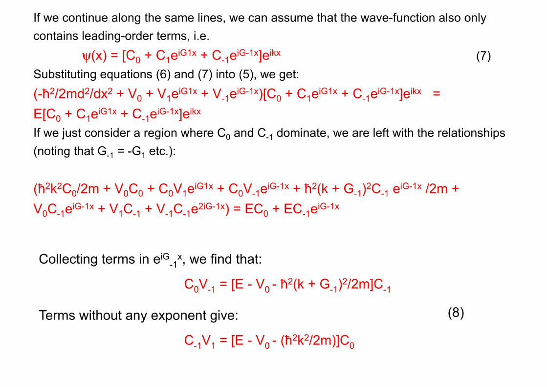
If we continue along the same lines, we can assume that the wave-function also only contains leading-order terms, i.e.
ψ(x) = [C0 + C1eiG1x + C-1eiG-1x]eikx (7) Substituting equations (6) and (7) into (5), we get: (-ħ2/2md2/dx2 + V0 + V1eiG1x + V-1eiG-1x)[C0 + C1eiG1x + C-1eiG-1x]eikx = E[C0 + C1eiG1x + C-1eiG-1x]eikx If we just consider a region where C0 and C-1 dominate, we are left with the relationships (noting that G-1 = -G1 etc.):
Solving for E in terms of k, and plotting, we get a relationship of the form:
Vo
= 2V1
5
10
15
20
25
30
-1.5 -1 -0.5 0 0.5 1 1.5
k
E G
E c
Points of interest to note relative to free-electron case: The energy is shifted up by the amount V0, where V0 is the spatial average of V(x) At certain values of k, the terms in brackets in Equation (8) are equal, i.e. at k = -G-1/2 = π/a. The gaps appear at these points, which define the Brillouin Zone boundary, and this corresponds to Bragg reflection. At this value of k, the energy can have two values:
E = V0 + (ħ2(π/a)2)/2m ± |V1| The separation in energy is 2|V1|, which is just twice the first term in the Fourier series expansion of the crystal potential, and the Schrödinger equation has no wave-like solutions in this gap The wavefunction at the energy gap has two solutions corresponding to:
ψ±(x) = C0[1 ± e(-2iπx/a)]e(iπx/a) or,
ψ-(x) = i2C0sin(πx/a) and ψ+(x) = 2C0cos(πx/a) These are standing waves! i.e., electrons at these energies cannot travel through the crystal, and hence do not contribute to conduction.
Now, ψ+(x) is the lower energy state, and has maxima at the atomic cores, whereas ψ-(x) is the higher energy state, with maxima at the mid-points between the atomic cores. These correspond to the valence and conduction bands, respectively.
How do we draw band diagrams? There are two methods: the extended and reduced-zone schemes.
Extended zone scheme Reduced zone scheme
In the reduced zone scheme, we just shift everything in order to show all the bands as lying within the first Brillouin zone.
The first band is always full, and often the second band is more than half-full.
Conduction band
valence band
Interesting point: The electronic wave-functions outside the energy gap are described by travelling
waves superimposed on a (Bloch) function with the lattice periodicity. On average then, the electrons are represented as travelling waves, with equal probability of being anywhere within the conductor; i.e. from this model, there is no reason for electrical resistance - electrons should move unhindered throughout a metal! We will see later in the course that electrical resistance is caused by deviations from the lattice periodicity.
More about band structure
Metals: electrons carry current Semiconductors: electrons & holes. Both types of carrier have distinct band structure, i.e. the conduction & valence bands respectively. Real materials have significantly more complex band structure, as they are 3-Dimensional! Also, for most materials, the atomic spacings are not the same in all directions, so the apparent band gap can seem different depending on which direction an electron is travelling in!
Si Band structure
Electrons (conduction band)
holes (valence band)
Depending on the relative position of the conduction band minimum to the valence band maximum, we have either direct or indirect gap semiconductors.
Direct gap Indirect gap In a direct-gap semiconductor (e.g. GaAs, Ge), to cause a transition of an electron from the
Valence band to the Conduction band only requires energy (Eg), whereas in an indirect-gap semiconductor (e.g. Si), momentum (q) is also required. Therefore, only direct-gap semiconductors can be used in optical devices (e.g. photodiodes). The momentum of a photon is generally extremely small, and not enough to induce a transition, so the transition must involve something else (known as a phonon, which we will see later).
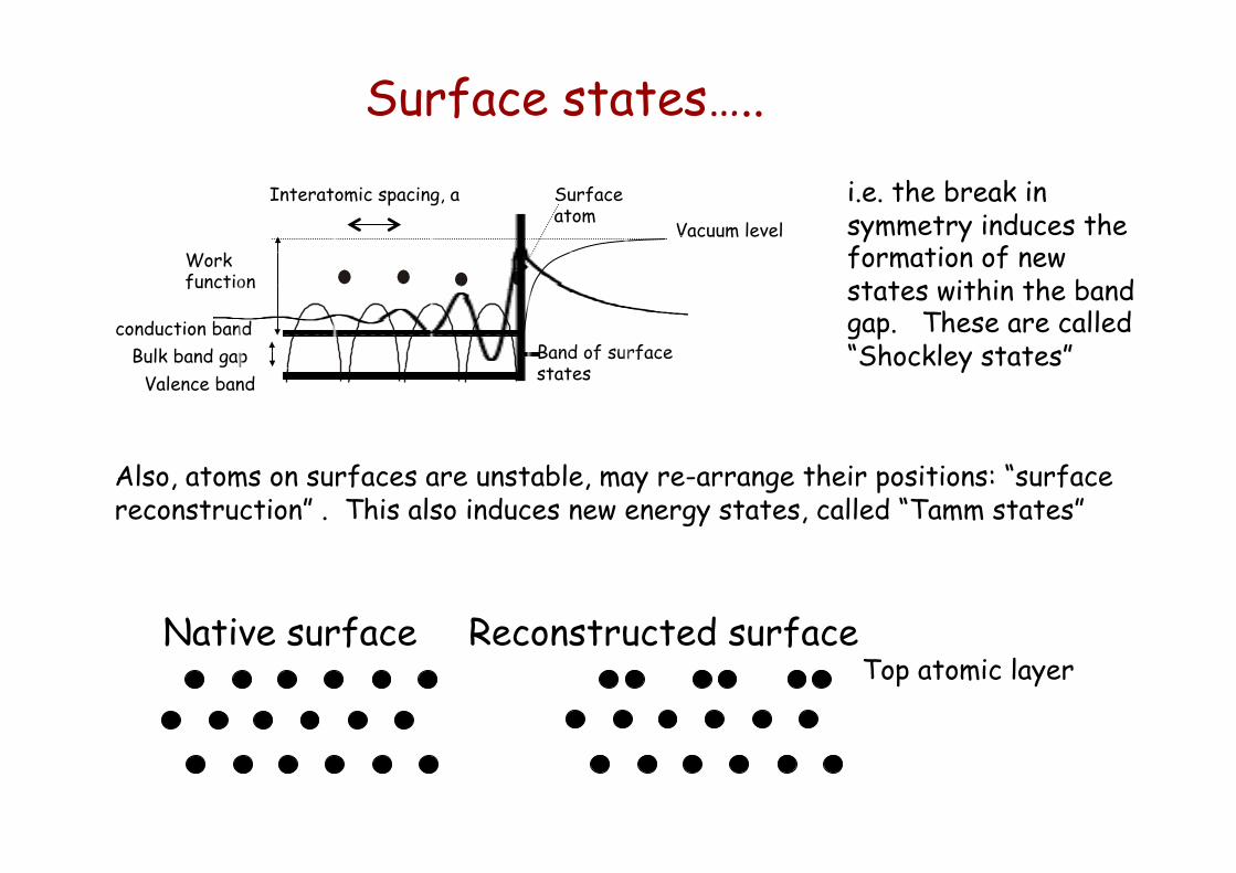
Surface states…..
Surface atom
Interatomic spacing, a
Bulk band gap
Vacuum level Work function
Valence band
conduction band Band of surface states
Native surface Reconstructed surface Top atomic layer
i.e. the break in symmetry induces the formation of new states within the band gap. These are called “Shockley states”
Also, atoms on surfaces are unstable, may re-arrange their positions: “surface reconstruction” . This also induces new energy states, called “Tamm states”