M93S66, M93S56, M93S46 4K/2K/1K (x16) Serial Microwire Bus EEPROM with Block Protection February 1999 1/23 AI02020 D V CC M93Sx6 V SS C Q PRE W S Figure 1. Logic Diagram INDUSTRY STANDARD MICROWIRE BUS 1 MILLION ERASE/WRITE CYCLES, with 40 YEARS DATA RETENTION SINGLE ORGANIZATION by WORD (x16) WORD and ENTIRE MEMORY PROGRAMMING INSTRUCTIONS SELF-TIMED PROGRAMMING CYCLE with AUTO-ERASE READY/BUSY SIGNAL DURING PROGRAMMING SINGLE SUPPLY VOLTAGE: – 4.5V to 5.5V for M93Sx6 version – 2.5V to 5.5V for M93Sx6-W version – 1.8V to 3.6V for M93Sx6-R version USER DEFINED WRITE PROTECTED AREA PAGE WRITE MODE (4 words) SEQUENTIAL READ OPERATION 5ms TYPICAL PROGRAMMING TIME ENHANCED ESD and LATCH-UP PERFORMANCES DESCRIPTION This M93S46/S56/S66 specification covers a range of 4K/2K/1K bit serial EEPROM products respectively. In this text, products are referred to as M93Sx6. The M93Sx6 is an Electrically Erasable Programmable Memory (EEPROM) fabricated with STMicroelectronics’s High Endurance Single Polysilicon CMOS technology. S Chip Select Input D Serial Data Input Q Serial Data Output C Serial Clock PRE Protect Enable W Write Enable V CC Supply Voltage V SS Ground Table 1. Signal Names 8 1 SO8 (MN) 150mil Width 8 1 PSDIP8 (BN) 0.25mm Frame 8 1 TSSOP8 (DW) 169mil Width
Transcript
M93S66, M93S56, M93S46
4K/2K/1K (x16) Serial Microwire Bus EEPROM with Block Protection
February 1999 1/23
AI02020
D
VCC
M93Sx6
VSS
C Q
PRE
W
S
Figure 1. Logic Diagram
INDUSTRY STANDARD MICROWIRE BUS1 MILLION ERASE/WRITE CYCLES, with40 YEARS DATA RETENTIONSINGLE ORGANIZATION by WORD (x16)WORD and ENTIRE MEMORYPROGRAMMING INSTRUCTIONSSELF-TIMED PROGRAMMING CYCLE withAUTO-ERASEREADY/BUSY SIGNAL DURINGPROGRAMMINGSINGLE SUPPLY VOLTAGE:– 4.5V to 5.5V for M93Sx6 version– 2.5V to 5.5V for M93Sx6-W version– 1.8V to 3.6V for M93Sx6-R version USER DEFINED WRITE PROTECTED AREAPAGE WRITE MODE (4 words)SEQUENTIAL READ OPERATION5ms TYPICAL PROGRAMMING TIMEENHANCED ESD and LATCH-UPPERFORMANCES
DESCRIPTIONThis M93S46/S56/S66 specification covers arange of 4K/2K/1K bit serial EEPROM productsrespectively. In this text, products are referred to asM93Sx6. The M93Sx6 is an Electrically ErasableProgrammable Memory (EEPROM) fabricated withSTMicroelectronics’s High Endurance SinglePolysilicon CMOS technology.
S Chip Select Input
D Serial Data Input
Q Serial Data Output
C Serial Clock
PRE Protect Enable
W Write Enable
VCC Supply Voltage
VSS Ground
Table 1. Signal Names
8
1
SO8 (MN)150mil Width
8
1
PSDIP8 (BN)0.25mm Frame
8
1
TSSOP8 (DW)169mil Width
The M93Sx6 memory is accessed through a serialinput (D) and output (Q) using the MICROWIREbus protocol. The M93Sx6 is specified at 5V ±10%,the M93Sx6-W specified at 2.5V to 5.5V and theM93Sx6-R specified at 1.8V to 3.6V.The M93S66/S56/S46 memory is divided into256/128/64 x16 bit words respectively. Thesememory devices are available in both PSDIP8,SO8 and TSSOP8 packages.The M93Sx6 memory is accessed by a set ofinstructions which includes Read, Write, Page
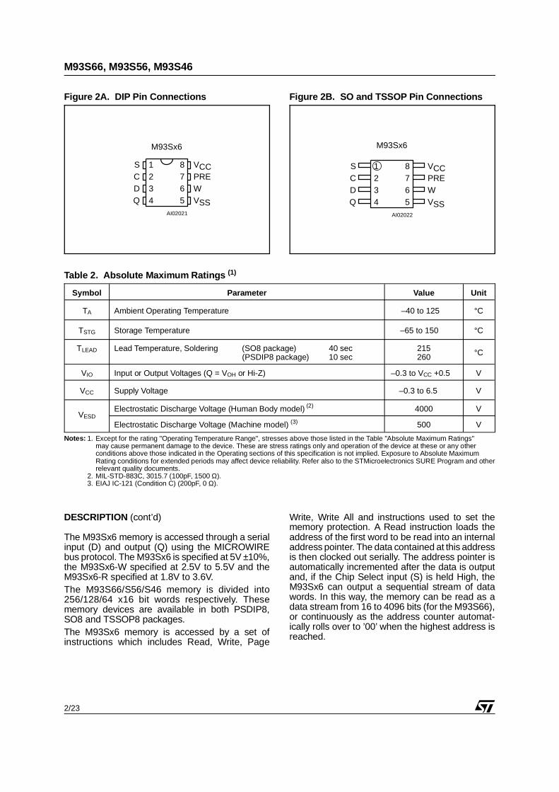
VSSQWPREC
S VCC
D
AI02021
M93Sx6
1234
8765
Figure 2A. DIP Pin Connections
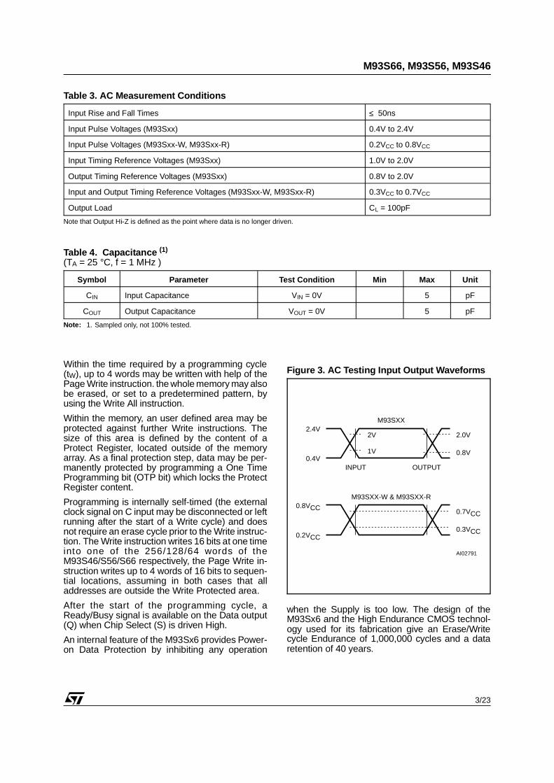
1
VSSQWPREC
S VCC
D
AI02022
M93Sx6
234
8765
Figure 2B. SO and TSSOP Pin Connections
DESCRIPTION (cont’d) Write, Write All and instructions used to set thememory protection. A Read instruction loads theaddress of the first word to be read into an internaladdress pointer. The data contained at this addressis then clocked out serially. The address pointer isautomatically incremented after the data is outputand, if the Chip Select input (S) is held High, theM93Sx6 can output a sequential stream of datawords. In this way, the memory can be read as adata stream from 16 to 4096 bits (for the M93S66),or continuously as the address counter automat-ically rolls over to ’00’ when the highest address isreached.
Symbol Parameter Value Unit
TA Ambient Operating Temperature –40 to 125 °C
TSTG Storage Temperature –65 to 150 °C
TLEAD Lead Temperature, Soldering (SO8 package)(PSDIP8 package)
40 sec10 sec
215260 °C
VIO Input or Output Voltages (Q = VOH or Hi-Z) –0.3 to VCC +0.5 V
VCC Supply Voltage –0.3 to 6.5 V
VESDElectrostatic Discharge Voltage (Human Body model) (2) 4000 V
Electrostatic Discharge Voltage (Machine model) (3) 500 V
Notes: 1. Except for the rating "Operating Temperature Range", stresses above those listed in the Table "Absolute Maximum Ratings" may cause permanent damage to the device. These are stress ratings only and operation of the device at these or any other conditions above those indicated in the Operating sections of this specification is not implied. Exposure to Absolute Maximum Rating conditions for extended periods may affect device reliability. Refer also to the STMicroelectronics SURE Program and other relevant quality documents.
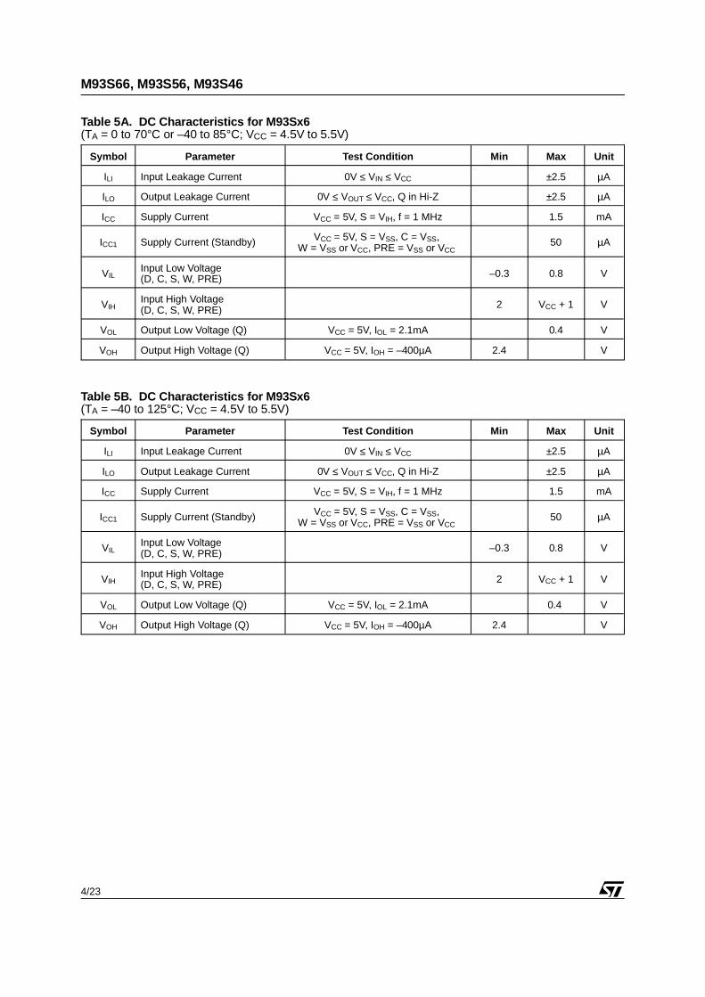
Input Pulse Voltages (M93Sxx-W, M93Sxx-R) 0.2VCC to 0.8VCC
Input Timing Reference Voltages (M93Sxx) 1.0V to 2.0V
Output Timing Reference Voltages (M93Sxx) 0.8V to 2.0V
Input and Output Timing Reference Voltages (M93Sxx-W, M93Sxx-R) 0.3VCC to 0.7VCC
Output Load CL = 100pF
Note that Output Hi-Z is defined as the point where data is no longer driven.
Table 3. AC Measurement Conditions
AI02791
2.4V
0.4V
2.0V
0.8V
2V
1V
INPUT OUTPUT
0.8VCC
0.2VCC
0.7VCC
0.3VCC
M93SXX-W & M93SXX-R
M93SXX
Figure 3. AC Testing Input Output Waveforms
Symbol Parameter Test Condition Min Max Unit
CIN Input Capacitance VIN = 0V 5 pF
COUT Output Capacitance VOUT = 0V 5 pF
Note: 1. Sampled only, not 100% tested.
Table 4. Capacitance (1) (TA = 25 °C, f = 1 MHz )
Within the time required by a programming cycle(tW), up to 4 words may be written with help of thePage Write instruction. the whole memory may alsobe erased, or set to a predetermined pattern, byusing the Write All instruction.
Within the memory, an user defined area may beprotected against further Write instructions. Thesize of this area is defined by the content of aProtect Register, located outside of the memoryarray. As a final protection step, data may be per-manently protected by programming a One TimeProgramming bit (OTP bit) which locks the ProtectRegister content.
Programming is internally self-timed (the externalclock signal on C input may be disconnected or leftrunning after the start of a Write cycle) and doesnot require an erase cycle prior to the Write instruc-tion. The Write instruction writes 16 bits at one timeinto one of the 256/128/64 words of theM93S46/S56/S66 respectively, the Page Write in-struction writes up to 4 words of 16 bits to sequen-tial locations, assuming in both cases that alladdresses are outside the Write Protected area.
After the start of the programming cycle, aReady/Busy signal is available on the Data output(Q) when Chip Select (S) is driven High.
An internal feature of the M93Sx6 provides Power-on Data Protection by inhibiting any operation
when the Supply is too low. The design of theM93Sx6 and the High Endurance CMOS technol-ogy used for its fabrication give an Erase/Writecycle Endurance of 1,000,000 cycles and a dataretention of 40 years.
3/23
M93S66, M93S56, M93S46
Symbol Parameter Test Condition Min Max Unit
ILI Input Leakage Current 0V ≤ VIN ≤ VCC ±2.5 µA
ILO Output Leakage Current 0V ≤ VOUT ≤ VCC, Q in Hi-Z ±2.5 µA
ICC Supply Current VCC = 5V, S = VIH, f = 1 MHz 1.5 mA
ICC1 Supply Current (Standby) VCC = 5V, S = VSS, C = VSS, W = VSS or VCC, PRE = VSS or VCC 50 µA
VILInput Low Voltage (D, C, S, W, PRE) –0.3 0.8 V
VIHInput High Voltage (D, C, S, W, PRE) 2 VCC + 1 V
VOL Output Low Voltage (Q) VCC = 5V, IOL = 2.1mA 0.4 V
VOH Output High Voltage (Q) VCC = 5V, IOH = –400µA 2.4 V
Table 5A. DC Characteristics for M93Sx6 (TA = 0 to 70°C or –40 to 85°C; VCC = 4.5V to 5.5V)
Symbol Parameter Test Condition Min Max Unit
ILI Input Leakage Current 0V ≤ VIN ≤ VCC ±2.5 µA
ILO Output Leakage Current 0V ≤ VOUT ≤ VCC, Q in Hi-Z ±2.5 µA
ICC Supply Current VCC = 5V, S = VIH, f = 1 MHz 1.5 mA
ICC1 Supply Current (Standby) VCC = 5V, S = VSS, C = VSS, W = VSS or VCC, PRE = VSS or VCC 50 µA
VILInput Low Voltage (D, C, S, W, PRE) –0.3 0.8 V
VIHInput High Voltage (D, C, S, W, PRE) 2 VCC + 1 V
VOL Output Low Voltage (Q) VCC = 5V, IOL = 2.1mA 0.4 V
VOH Output High Voltage (Q) VCC = 5V, IOH = –400µA 2.4 V
Table 5B. DC Characteristics for M93Sx6 (TA = –40 to 125°C; VCC = 4.5V to 5.5V)
4/23
M93S66, M93S56, M93S46
Symbol Parameter Test Condition Min Max Unit
ILI Input Leakage Current 0V ≤ VIN ≤ VCC ±2.5 µA
ILO Output Leakage Current 0V ≤ VOUT ≤ VCC, Q in Hi-Z ±2.5 µA
ICC Supply Current (CMOS Inputs)VCC = 5V, S = VIH, f = 1 MHz 1.5 mA
VCC = 2.5V, S = VIH, f = 1 MHz 1 mA
ICC1 Supply Current (Standby) VCC = 2.5V, S = VSS, C = VSS, W = VSS or VCC, PRE = VSS or VCC 10 µA
VILInput Low Voltage (D, C, S, W, PRE) –0.3 0.2 VCC V
VIHInput High Voltage (D, C, S, W, PRE) 0.7 VCC VCC + 1 V
VOL Output Low Voltage (Q)VCC = 5V, IOL = 2.1mA 0.4 V
VCC = 2.5V, IOL = 100µA 0.2 V
VOH Output High Voltage (Q)VCC = 5V, IOH = –400µA 2.4 V
VCC = 2.5V, IOH = –100µA VCC – 0.2 V
Table 5C. DC Characteristics for M93Sx6-W(TA = 0 to 70°C or –40 to 85°C; VCC = 2.5V to 5.5V)
Symbol Parameter Test Condition Min Max Unit
ILI Input Leakage Current 0V ≤ VIN ≤ VCC ±2.5 µA
ILO Output Leakage Current 0V ≤ VOUT ≤ VCC, Q in Hi-Z ±2.5 µA
ICC Supply Current (CMOS Inputs)VCC = 3.6V, S = VIH, f = 1 MHz 1.5 mA
VCC = 1.8V, S = VIH, f = 1 MHz 1 mA
ICC1 Supply Current (Standby) VCC = 1.8V, S = VSS, C = VSS, W = VSS or VCC, PRE = VSS or VCC 5 µA
VILInput Low Voltage (D, C, S, W, PRE) –0.3 0.2 VCC V
VIHInput High Voltage (D, C, S, W, PRE) 0.8 VCC VCC + 1 V
VOL Output Low Voltage (Q) VCC = 1.8V, IOL = 100µA 0.2 V
VOH Output High Voltage (Q) VCC = 1.8V, IOH = –100µA VCC – 0.2 V
Note: 1. This is preliminary data.
Table 5D. DC Characteristics for M93Sx6-R (1) (TA = 0 to 70°C or –20 to 85°C; VCC = 1.8V to3.6V)
5/23
M93S66, M93S56, M93S46
Symbol Alt Parameter
M93S66/56/46
UnitVCC = 4.5V to 5.5V,TA = 0 to 70°C,
TA = –40 to 85°C
VCC = 4.5V to 5.5V,TA = –40 to 125°C
Min Max Min Max
tPRVCH tPRES Protect Enable Valid to Clock High 50 50 ns
tWVCH tPES Write Enable Valid to Clock High 50 50 ns
tSHCH tCSS Chip Select Set-up Time 50 50 ns
tCLSH tSKS Clock Set-up Time (relative to S) 100 100 ns
tDVCH tDIS Data In Set-up Time 100 100 ns
tCHDX tDIH Data In Hold Time 100 100 ns
tCHQL tPD0 Delay to Output Low 400 400 ns
tCHQV tPD1 Delay to Output Valid 400 400 ns
tCLPRX tPREHClock Low to Protect Enable Transition 0 0 ns
Notes: 1. Chip Select must be brought low for a minimum of tSLSH between consecutive instructions cycles.2. The Clock frequency specification calls for a minimum clock period of 1/fC, therefore the sum of the timings tCHCL+tCLCH
must be greater or equal to 1/fC.
Table 6A. AC Characteristics
6/23
M93S66, M93S56, M93S46
Symbol Alt Parameter
M93S66/56/46
UnitVCC = 2.5V to 5.5V,TA = 0 to 70°C,
TA = –40 to 85°C
VCC = 1.8V to 3.6V, (3)
TA = 0 to 70°CTA = –20 to 85°C
Min Max Min Max
tPRVCH tPRES Protect Enable Valid to Clock High 50 50 ns
tWVCH tPES Write Enable Valid to Clock High 50 50 ns
tSHCH tCSS Chip Select Set-up Time 100 200 ns
tCLSH tSKS Clock Set-up Time (relative to S) 100 100 ns
tDVCH tDIS Data In Set-up Time 100 100 ns
tCHDX tDIH Data In Hold Time 100 200 ns
tCHQL tPD0 Delay to Output Low 400 700 ns
tCHQV tPD1 Delay to Output Valid 400 700 ns
tCLPRX tPREHClock Low to Protect Enable Transition 0 0 ns
Notes: 1. Chip Select must be brought low for a minimum of tSLSH between consecutive instructions cycles.2. The Clock frequency specification calls for a minimum clock period of 1/fC, therefore the sum of the timings tCHCL+tCLCH
must be greater or equal to 1/fC. 3. This is preliminary data.
Table 6B. AC Characteristics
7/23
M93S66, M93S56, M93S46
PRE
W
C
S
D OP CODE OP CODESTART
STARTOP CODE INPUT
tCHDXtDVCH
tCLSH tCLCH
tCHCLtWVCH
tPRVCH
AI02025
tSHCH
Figure 4. Synchronous Timing, Start and Op-Code Input
POWER-ON DATA PROTECTIONIn order to prevent data corruption and inadvertentwrite operations during power-up and power-down,a Power On Reset (POR) circuit resets all internalprogramming circuitry and sets the device in theWrite Disable mode. – At Power-up and Power-down, the device
must NOT be selected (that is, the S inputmust be driven low) until the supply voltagereaches the operating value Vcc specified inthe AC and DC tables.
– When VCC reaches its functional value, the de-vice is properly reset (in the Write Disablemode) and is ready to decode and execute anincoming instruction.
For the M93Sx6 specified at 5V, the POR thresholdvoltage is around 3V.For all the other M93Sx6 specified at low VCC (with-W and -R VCC range options), the POR thresholdvoltage is around 1.5V.
8/23
M93S66, M93S56, M93S46
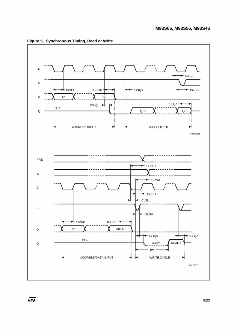
Figure 5. Synchronous Timing, Read or Write
AI002026
C
D
Q
ADDRESS INPUT
Hi-Z
tDVCH
tCLSL
A0
S
DATA OUTPUT
tCHQVtCHDX
tCHQL
An
tSLSH
tSLQZ
Q15 Q0
PRE
W
C
S
D
Hi-Z
tW
tDVCH
AI02027
Q
tCLPRX
tSLWX
tCLSL
tCHDX
tSLSH
tSLQZ
BUSY
tSHQV
READY
WRITE CYCLEADDRESS/DATA INPUT
An A0/D0
tSLCH
9/23
M93S66, M93S56, M93S46
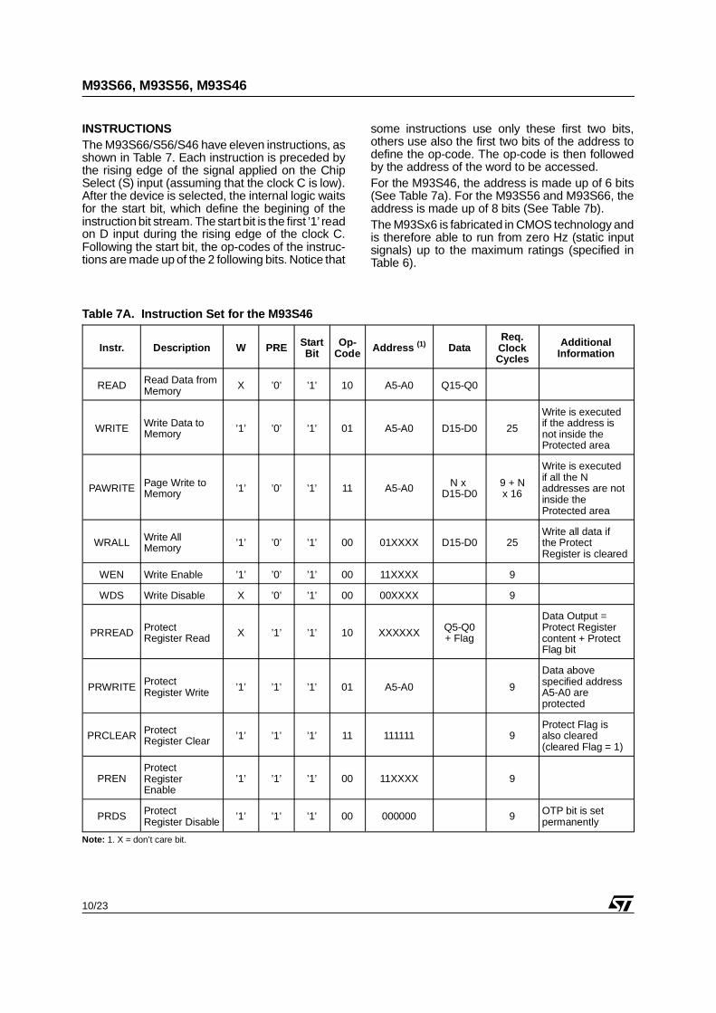
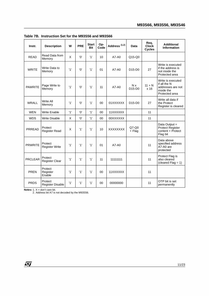
INSTRUCTIONSThe M93S66/S56/S46 have eleven instructions, asshown in Table 7. Each instruction is preceded bythe rising edge of the signal applied on the ChipSelect (S) input (assuming that the clock C is low).After the device is selected, the internal logic waitsfor the start bit, which define the begining of theinstruction bit stream. The start bit is the first ’1’ readon D input during the rising edge of the clock C.Following the start bit, the op-codes of the instruc-tions are made up of the 2 following bits. Notice that
some instructions use only these first two bits,others use also the first two bits of the address todefine the op-code. The op-code is then followedby the address of the word to be accessed.For the M93S46, the address is made up of 6 bits(See Table 7a). For the M93S56 and M93S66, theaddress is made up of 8 bits (See Table 7b).The M93Sx6 is fabricated in CMOS technology andis therefore able to run from zero Hz (static inputsignals) up to the maximum ratings (specified inTable 6).
Instr. Description W PRE StartBit
Op-Code Address (1) Data
Req.ClockCycles
AdditionalInformation
READ Read Data fromMemory X ’0’ ’1’ 10 A5-A0 Q15-Q0
PRDS ProtectRegister Disable ’1’ ’1’ ’1’ 00 00000000 11 OTP bit is set
permanently
Notes: 1. X = don’t care bit.2. Address bit A7 is not decoded by the M93S56.
Table 7B. Instruction Set for the M93S56 and M93S66
11/23
M93S66, M93S56, M93S46
ReadThe Read instruction (READ) outputs serial dataon the Data Output (Q). When a READ instructionis received, the instruction and address are de-coded and the data from the memory is transferredinto an output shift register. A dummy ’0’ bit is outputfirst followed by the 16 bit word with the MSB first.Output data changes are triggered by the Low toHigh transition of the Clock (C). The M93Sx6 willautomatically increment the address and will clockout the next word as long as the Chip Select input(S) is held High. In this case the dummy ’0’ bit isNOT output between words and a continuousstream of data can be read.Write Enable and Write DisableThe Write Enable instruction (WEN) authorizes thefollowing Write instructions to be executed. TheWrite Disable instruction (WDS) disables the exe-cution of the following Write instructions and theinternal programming cycle cannot run.When power is first applied, the M93Sx6 is in WriteDisable mode and all Write instructions are inhib-ited. When the WEN instruction is executed, Writeinstructions remain enabled until a Write Disableinstruction (WDS) is executed or VCC falls belowthe Power-On Reset threshold Voltage.To protect the memory contents from accidentalcorruption, it is advisable to issue the WDS instruc-tion after every write cycle. The READ instructionis not affected by the WEN or WDS instructions.WriteThe Write instruction (WRITE) is composed of theStart bit plus the Op-Code followed by the addressand the 16 data bits to be written. The Write Enablesignal (W) must be held high during the Writeinstruction. Data input (D) is sampled on the Lowto High transition of the clock. After the last data bithas been sampled, Chip Select (S) must bebrought Low before the next rising edge of the clock(C) in order to start the self-timed programmingcycle. This is really important as, if S is brought lowbefore or after this specific frame window, theaddressed location will not be programmed, provid-ing that the address in NOT in the protected area.If the M93Sx6 is still performing the write cycle, theBusy signal (Q = 0) will be returned if the ChipSelect input (S) is driven high after the tSLSH delay,and the M93Sx6 will ignore any data on the bus.When the write cycle is completed, the Readysignal (Q = 1) will indicate (if S is driven high) thatthe M93Sx6 is ready to receive a new instruction.Programming is internally self-timed (the externalclock signal on C input may be disconnected or leftrunning after the start of a Write cycle).
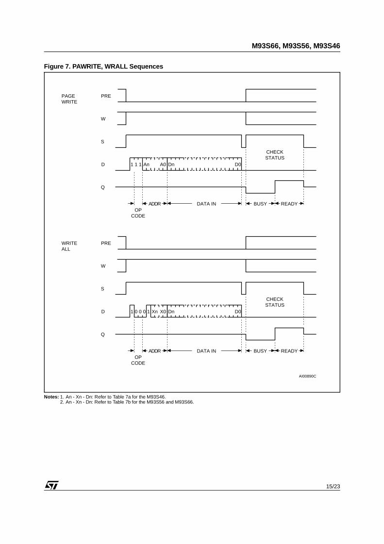
Page WriteA Page Write instruction (PAWRITE) contains thefirst address to be written followed by up to 4 datawords. The Write Enable signal (W) must be heldHigh during the PAWRITE instruction. Input ad-dress and data are sampled on the Low to Hightransition of the clock. After the receipt of each dataword, bits A1-A0 of the internal address register areincremented, the high order bits (Ax-A2) remainingunchanged. Users must take care by software toensure that the last word address has the sameupper order address bits as the initial addresstransmitted to avoid address roll-over. After the LSBof the last data word, Chip Select (S) must bebrought Low before the next rising edge of theClock (C) in order to start the self-timed program-ming cycle. This is really important as, if S isbrought low before or after this specific frame win-dow, the addressed locations will not be pro-grammed. The Page Write operation will not beperformed if any of the 4 words is addressing theprotected area. If the M93Sx6 is still performing theprogramming cycle, the Busy signal (Q = 0) will bereturned if the Chip Select input (S) is driven high,and the M93Sx6 will ignore any data on the bus.When the write cycle is completed, the Readysignal (Q = 1) will indicate (if S is driven high) thatthe M93Sx6 is ready to receive a new instruction.
Write AllThe Write All instruction (WRALL) is valid only afterthe Protect Register has been cleared by executinga PRCLEAR (Protect Register Clear) instruction.The Write All instruction simultaneously writes thewhole memory with the same data word includedin the instruction. The Write Enable signal (W) mustbe held High before and during the Write All instruc-tion. Input address and data are sampled on theLow to High transition of the clock. If the M93Sx6is still performing the write cycle, the Busy signal(Q = 0) will be returned if the Chip Select input (S)is driven high after the tSLSH delay, and the M93Sx6will ignore any data on the bus. When the writecycle is completed, the Ready signal (Q = 1) willindicate (if S is driven high) that the M93Sx6 isready to receive a new instruction.
READY/BUSY StatusDuring every programming cycle (after a WRITE,WRALL or PAWRITE instruction) the Data Output(Q) indicates the Ready/Busy status of the memorywhen the Chip Select is driven High. Once theM93Sx6 is Ready, the Data Output is set to ’1’ untila new start bit is decoded or the Chip Select isbrought Low.
12/23
M93S66, M93S56, M93S46
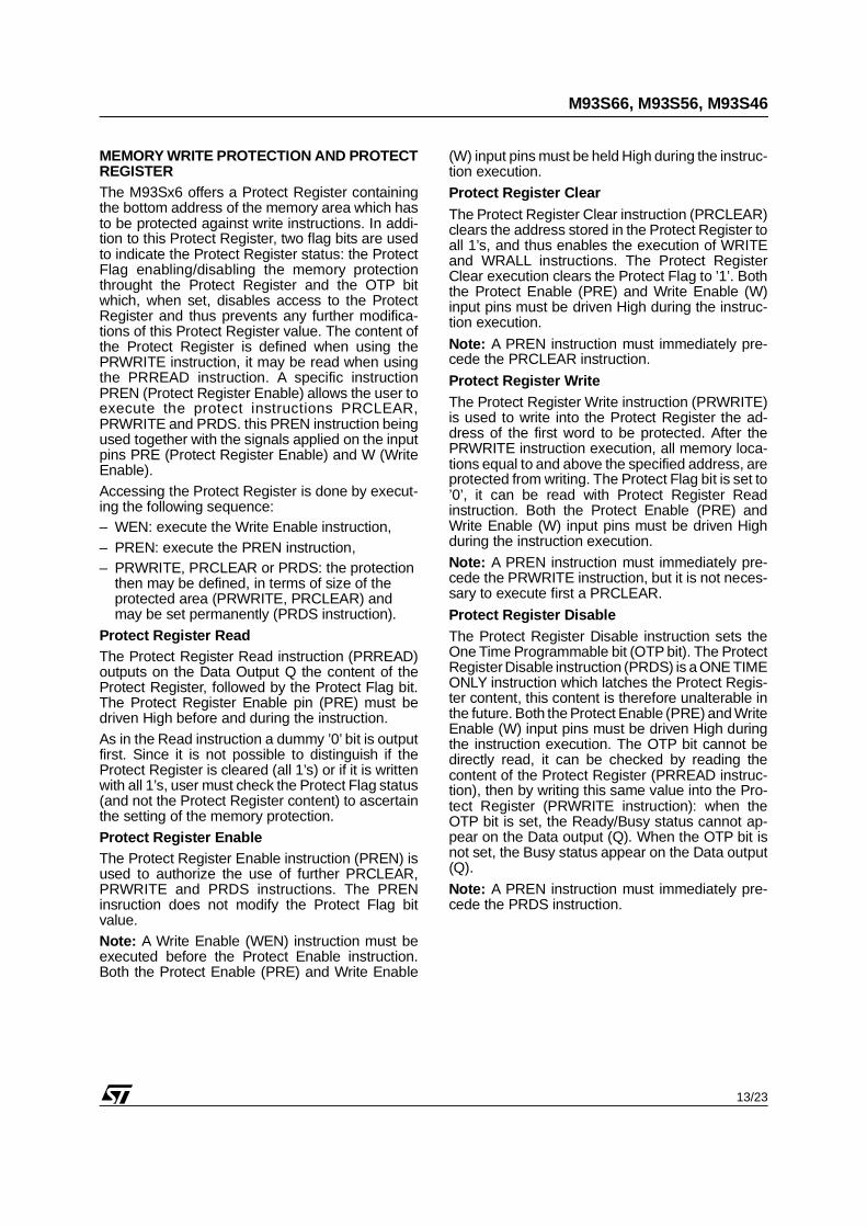
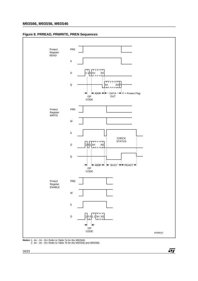
MEMORY WRITE PROTECTION AND PROTECTREGISTERThe M93Sx6 offers a Protect Register containingthe bottom address of the memory area which hasto be protected against write instructions. In addi-tion to this Protect Register, two flag bits are usedto indicate the Protect Register status: the ProtectFlag enabling/disabling the memory protectionthrought the Protect Register and the OTP bitwhich, when set, disables access to the ProtectRegister and thus prevents any further modifica-tions of this Protect Register value. The content ofthe Protect Register is defined when using thePRWRITE instruction, it may be read when usingthe PRREAD instruction. A specific instructionPREN (Protect Register Enable) allows the user toexecute the protect instructions PRCLEAR,PRWRITE and PRDS. this PREN instruction beingused together with the signals applied on the inputpins PRE (Protect Register Enable) and W (WriteEnable).Accessing the Protect Register is done by execut-ing the following sequence:– WEN: execute the Write Enable instruction, – PREN: execute the PREN instruction, – PRWRITE, PRCLEAR or PRDS: the protection
then may be defined, in terms of size of theprotected area (PRWRITE, PRCLEAR) andmay be set permanently (PRDS instruction).
Protect Register ReadThe Protect Register Read instruction (PRREAD)outputs on the Data Output Q the content of theProtect Register, followed by the Protect Flag bit.The Protect Register Enable pin (PRE) must bedriven High before and during the instruction.As in the Read instruction a dummy ’0’ bit is outputfirst. Since it is not possible to distinguish if theProtect Register is cleared (all 1’s) or if it is writtenwith all 1’s, user must check the Protect Flag status(and not the Protect Register content) to ascertainthe setting of the memory protection.
Protect Register Enable The Protect Register Enable instruction (PREN) isused to authorize the use of further PRCLEAR,PRWRITE and PRDS instructions. The PRENinsruction does not modify the Protect Flag bitvalue. Note: A Write Enable (WEN) instruction must beexecuted before the Protect Enable instruction.Both the Protect Enable (PRE) and Write Enable
(W) input pins must be held High during the instruc-tion execution.
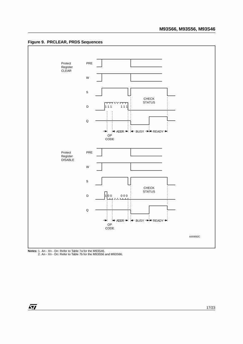
Protect Register ClearThe Protect Register Clear instruction (PRCLEAR)clears the address stored in the Protect Register toall 1’s, and thus enables the execution of WRITEand WRALL instructions. The Protect RegisterClear execution clears the Protect Flag to ’1’. Boththe Protect Enable (PRE) and Write Enable (W)input pins must be driven High during the instruc-tion execution.
Note: A PREN instruction must immediately pre-cede the PRCLEAR instruction.
Protect Register WriteThe Protect Register Write instruction (PRWRITE)is used to write into the Protect Register the ad-dress of the first word to be protected. After thePRWRITE instruction execution, all memory loca-tions equal to and above the specified address, areprotected from writing. The Protect Flag bit is set to’0’, it can be read with Protect Register Readinstruction. Both the Protect Enable (PRE) andWrite Enable (W) input pins must be driven Highduring the instruction execution.
Note: A PREN instruction must immediately pre-cede the PRWRITE instruction, but it is not neces-sary to execute first a PRCLEAR.
Protect Register DisableThe Protect Register Disable instruction sets theOne Time Programmable bit (OTP bit). The ProtectRegister Disable instruction (PRDS) is a ONE TIMEONLY instruction which latches the Protect Regis-ter content, this content is therefore unalterable inthe future. Both the Protect Enable (PRE) and WriteEnable (W) input pins must be driven High duringthe instruction execution. The OTP bit cannot bedirectly read, it can be checked by reading thecontent of the Protect Register (PRREAD instruc-tion), then by writing this same value into the Pro-tect Register (PRWRITE instruction): when theOTP bit is set, the Ready/Busy status cannot ap-pear on the Data output (Q). When the OTP bit isnot set, the Busy status appear on the Data output(Q).
Note: A PREN instruction must immediately pre-cede the PRDS instruction.
13/23
M93S66, M93S56, M93S46
AI00889D
1 1 0 An A0
Qn Q0
DATA OUT
D
S
Q
S
WRITE
ADDROP
CODE
1 0 An A0
DATA IN
D
Q
OPCODE
Dn D01
BUSY READY
S
WRITEENABLE
1 0 Xn X0D
OPCODE
10 1
S
WRITEDISABLE
1 0 Xn X0D
OPCODE
0 00
CHECKSTATUS
ADDR
PREREAD
PRE
W
PRE
W
PRE
Figure 6. READ, WRITE, WEN, WDS Sequences
Notes: 1. An - Xn - Qn - Dn: Refer to Table 7a for the M93S46.2. An - Xn - Qn - Dn: Refer to Table 7b for the M93S56 and M93S66.
14/23
M93S66, M93S56, M93S46
AI00890C
S
PAGEWRITE
1 1 An A0
DATA IN
D
Q
OPCODE
Dn D01
BUSY READY
CHECKSTATUS
ADDR
PRE
W
S
WRITEALL
1 0 Xn X0
DATA IN
D
Q
OPCODE
Dn D00
BUSY READY
CHECKSTATUS
ADDR
PRE
W
0 1
Figure 7. PAWRITE, WRALL Sequences
Notes: 1. An - Xn - Dn: Refer to Table 7a for the M93S46.2. An - Xn - Dn: Refer to Table 7b for the M93S56 and M93S66.
15/23
M93S66, M93S56, M93S46
Notes: 1. An - Xn - Dn: Refer to Table 7a for the M93S46.2. An - Xn - Dn: Refer to Table 7b for the M93S56 and M93S66.
AI00891D
1 1 0 Xn X0
DATAOUT
D
S
Q
S
ProtectRegisterWRITE
ADDROP
CODE
1 0 An A0D
Q
OPCODE
1
BUSY READY
S
ProtectRegisterENABLE
1 0 Xn X0D
OPCODE
10 1
CHECKSTATUS
ADDR
PREProtectRegisterREAD
PRE
W
PRE
W
An A0 F
F = Protect Flag
Figure 8. PRREAD, PRWRITE, PREN Sequences
16/23
M93S66, M93S56, M93S46
Notes: 1. An - Xn - Dn: Refer to Table 7a for the M93S46.2. An - Xn - Dn: Refer to Table 7b for the M93S56 and M93S66.
AI00892C
S
ProtectRegisterCLEAR
1 1D
Q
OPCODE
1
BUSY READY
CHECKSTATUS
ADDR
PRE
W
1 1 1
S
ProtectRegisterDISABLE
1 0D
Q
OPCODE
0
BUSY READY
CHECKSTATUS
ADDR
PRE
W
0 0 0
Figure 9. PRCLEAR, PRDS Sequences
17/23
M93S66, M93S56, M93S46
AI01395
S
An-1
C
D
WRITE
START D0"1""0"
An
Glitch
An-2
ADDRESS AND DATAARE SHIFTED BY ONE BIT
Figure 10. Write Sequence with One Clock Glitch
COMMON I/O OPERATIONThe Data Output (Q) and Data Input (D) signals canbe connected together, through a current limitingresistor, to form a common, one wire data bus.Some precautions must be taken when operatingthe memory with this connection, mostly to preventa short circuit between the last entered address bit(A0) and the first data bit output by Q. The readershould refer to the STMicroelectronics applicationnote AN394 "MICROWIRE EEPROM Common I/OOperation".
CLOCK PULSE COUNTER
The M93Sx6 offers a functional security filteringglitches on the clock input (C), the clock pulsecounter.
In a normal environment, the M93Sx6 expectes toreceive the exact amount of data on the D input(start bit, Op-Code, Address, Data), that is theexact amount of clock pulses on the C input. In anoisy environment, the number of pulses received(on the clock input C) may be greater than the clock
pulses delivered by the Master (Microcontroller)driving the M93Sx6. In such a case, a part of theinstruction is delayed by one bit (see Figure 10),and it may induce an erroneous write of data at awrong address. The M93Sx6 has an on-chipcounter which counts the clock pulses from theStart bit until the falling edge of the Chip Selectsignal.For the WRITE instructions with a M93S56 (orM93S66), the number of clock pulses incoming tothe counter must be exactly 27 from the Start bit tothe falling edge of Chip Select signal (1 Start bit +2 Op-code bit + 8 Address bit + 16 Data bit = 27):if so, the M93S56 (or M93S66) executes theWRITE instruction. If the number of clock pulses isnot equal to 27, the instruction will not be executed(and data will not be corrupted).The clock pulse counter is active on WRITE,PAWRITE, WRALL, PRWRITE and PRCLEAR in-structions. In order to determine the exact numberof clock pulses needed for all the M93Sx6 onWRITE instructions, refer to Tables 7a and 7b, inthe column: Requested Clock Cycles.
18/23
M93S66, M93S56, M93S46
ORDERING INFORMATION SCHEME
Devices are shipped from the factory with the memory content set at all "1’s" (FFFFh).For a list of available options (Operating Voltage, Package, etc...) or for further information on any aspectof this device, please contact the STMicroelectronics Sales Office nearest to you.
Memory Density
66 4 Kbit
56 2 Kbit
46 1 Kbit
Operating Voltage
blank 4.5V to 5.5V
W 2.5V to 5.5V
R (3) 1.8V to 3.6V
Package
BN PSDIP80.25mm Frame
MN SO8150mil Width
DW TSSOP8169mil Width
Temperature Range
1 (1) 0 to 70 °C
5 –20 to 85 °C
6 –40 to 85 °C
3 (2) –40 to 125 °C
Option
T Tape & ReelPacking
Example: M93S56 – W MN 6 T
Notes: 1. Temperature range on request only. 2. Produced with High Reliability Certified Flow (HRCF), in VCC range 4.5V to 5.5V at 1MHz only.3. -R version (1.8V to 3.6V) are only available in temperature ranges 5 or 1.
19/23
M93S66, M93S56, M93S46
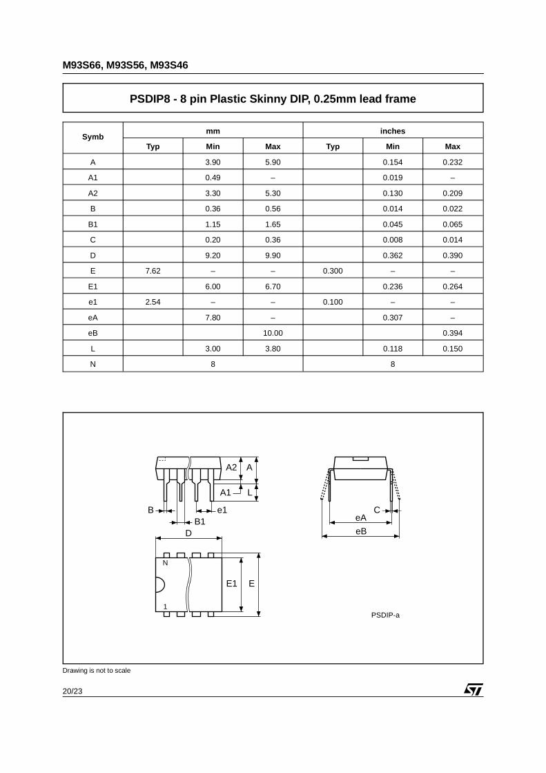
PSDIP-a
A2
A1
A
L
e1
D
E1 E
N
1
CeA
eBB1
B
Symbmm inches
Typ Min Max Typ Min Max
A 3.90 5.90 0.154 0.232
A1 0.49 – 0.019 –
A2 3.30 5.30 0.130 0.209
B 0.36 0.56 0.014 0.022
B1 1.15 1.65 0.045 0.065
C 0.20 0.36 0.008 0.014
D 9.20 9.90 0.362 0.390
E 7.62 – – 0.300 – –
E1 6.00 6.70 0.236 0.264
e1 2.54 – – 0.100 – –
eA 7.80 – 0.307 –
eB 10.00 0.394
L 3.00 3.80 0.118 0.150
N 8 8
Drawing is not to scale
PSDIP8 - 8 pin Plastic Skinny DIP, 0.25mm lead frame
20/23
M93S66, M93S56, M93S46
SO-a
E
N
CPB
e
A
D
C
LA1 α
1
H
h x 45˚
Symbmm inches
Typ Min Max Typ Min Max
A 1.35 1.75 0.053 0.069
A1 0.10 0.25 0.004 0.010
B 0.33 0.51 0.013 0.020
C 0.19 0.25 0.007 0.010
D 4.80 5.00 0.189 0.197
E 3.80 4.00 0.150 0.157
e 1.27 – – 0.050 – –
H 5.80 6.20 0.228 0.244
h 0.25 0.50 0.010 0.020
L 0.40 0.90 0.016 0.035
α 0° 8° 0° 8°
N 8 8
CP 0.10 0.004
Drawing is not to scale
SO8 - 8 lead Plastic Small Outline, 150 mils body width
21/23
M93S66, M93S56, M93S46
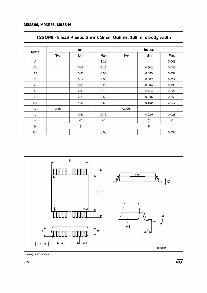
TSSOP
1
N
CP
N/2
DIE
C
LA1
EE1
D
A2A
α
eB
Symbmm inches
Typ Min Max Typ Min Max
A 1.10 0.043
A1 0.05 0.15 0.002 0.006
A2 0.85 0.95 0.033 0.037
B 0.19 0.30 0.007 0.012
C 0.09 0.20 0.004 0.008
D 2.90 3.10 0.114 0.122
E 6.25 6.50 0.246 0.256
E1 4.30 4.50 0.169 0.177
e 0.65 – – 0.026 – –
L 0.50 0.70 0.020 0.028
α 0° 8° 0° 8°
N 8 8
CP 0.08 0.003
Drawing is not to scale
TSSOP8 - 8 lead Plastic Shrink Small Outline, 169 mils body width
22/23
M93S66, M93S56, M93S46
Information furnished is believed to be accurate and reliable. However, STMicroelectronics assumes no responsibility for the consequencesof use of such information nor for any infringement of patents or other rights of third parties which may result from its use. No license is grantedby implication or otherwise under any patent or patent rights of STMicroelectronics. Specifications mentioned in this publication are subject tochange without notice. This publication supersedes and replaces all information previously supplied. STMicroelectronics products are notauthorized for use as critical components in life support devices or systems without express written approval of STMicroelectronics.
The ST logo is a registered trademark of STMicroelectronics
All other names are the property of their respective owners
STMicroelectronics GROUP OF COMPANIES Australia - Brazil - Canada - China - France - Germany - Italy - Japan - Korea - Malaysia - Malta - Mexico - Morocco - The Netherlands -
Singapore - Spain - Sweden - Switzerland - Taiwan - Thailand - United Kingdom - U.S.A.