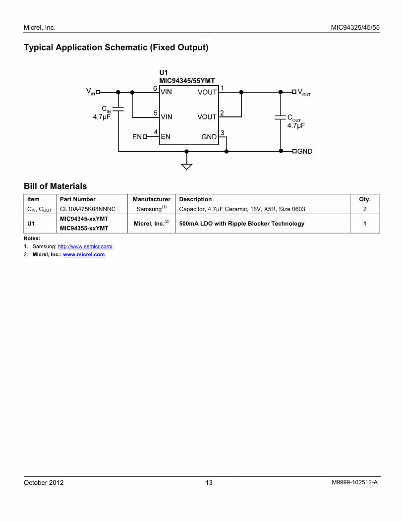
MIC94325/45/55 500mA LDO with Ripple BlockerTechnology Ripple Blocker is a trademark of Micrel, Inc Micrel Inc. • 2180 Fortune Drive • San Jose, CA 95131 • USA • tel +1 (408) 944-0800 • fax + 1 (408) 474-1000 • http://www.micrel.com General Description The MIC943x5 Ripple Blockeris a monolithic integrated circuit that provides low-frequency ripple attenuation (switching noise rejection) to a regulated output voltage. This is important for applications where a DC/DC switching converter is required to lower or raise a battery voltage but where switching noise cannot be tolerated by sensitive downstream circuits such as in RF applications. The MIC943x5 maintains high power supply ripple rejection (PSRR) with input voltages operating near the output voltage level to improve overall system efficiency. A low- voltage logic enable pin facilitates ON/OFF control at typical GPIO voltage levels. The MIC943x5 operates from an input voltage of 1.8V to 3.6V. The MIC943x5 options include fixed (MIC94345/55) or adjustable (MIC94325) output voltages. The MIC94355 version offers an auto-discharge to discharge the output capacitor when the part is disabled. Packaged in a 0.84mm x 1.32mm 6-ball CSP or a 6-pin 1.6mm x 1.6mm Thin DFN, the MIC943x5 has a junction operating temperature range of –40C to +125C. Data sheets and support documentation can be found on Micrel’s web site at: www.micrel.com . Features 1.8V to 3.6V input voltage range Active noise rejection over a wide frequency band >50dB from 10Hz to 5MHz at 500mA load Rated to 500mA output current Fixed and adjustable output voltages Optional output auto-discharge when disabled Current-limit and thermal-limit protected Ultra-small 0.84mm x 1.32mm 6-ball CSP 1.6mm x 1.6mm, 6-pin Thin DFN Logic-controlled enable pin 40C to +125C junction temperature range Applications Smart phones Tablet PC/notebooks and webcams Digital still and video cameras Global positioning systems Mobile computing Automotive and industrial applications _________________________________________________________________________________________________ Typical Application October 2012 M9999-102512-A MIC94355 PSRR C OUT = 4.7μF -120 -100 -80 -60 -40 -20 0 0 00 000 FREQUENCY (Hz) PSRR (dB) V IN = 2.8V + 40mVpp V OUT = 1.8V COUT = 4.7μF 10 100 1K 10K 100K 1M 10M 10mA 200mA 500mA
Transcript
MIC94325/45/55
500mA LDO with Ripple Blocker Technology
Ripple Blocker is a trademark of Micrel, Inc
Micrel Inc. • 2180 Fortune Drive • San Jose, CA 95131 • USA • tel +1 (408) 944-0800 • fax + 1 (408) 474-1000 • http://www.micrel.com
General Description The MIC943x5 Ripple Blocker is a monolithic integrated circuit that provides low-frequency ripple attenuation (switching noise rejection) to a regulated output voltage. This is important for applications where a DC/DC switching converter is required to lower or raise a battery voltage but where switching noise cannot be tolerated by sensitive downstream circuits such as in RF applications. The MIC943x5 maintains high power supply ripple rejection (PSRR) with input voltages operating near the output voltage level to improve overall system efficiency. A low-voltage logic enable pin facilitates ON/OFF control at typical GPIO voltage levels.
The MIC943x5 operates from an input voltage of 1.8V to 3.6V. The MIC943x5 options include fixed (MIC94345/55) or adjustable (MIC94325) output voltages. The MIC94355 version offers an auto-discharge to discharge the output capacitor when the part is disabled.
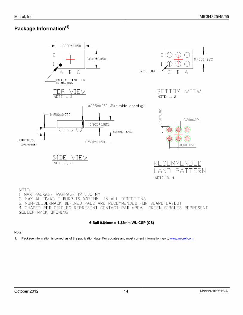
Packaged in a 0.84mm x 1.32mm 6-ball CSP or a 6-pin 1.6mm x 1.6mm Thin DFN, the MIC943x5 has a junction operating temperature range of –40C to +125C.
Data sheets and support documentation can be found on Micrel’s web site at: www.micrel.com.
Features 1.8V to 3.6V input voltage range
Active noise rejection over a wide frequency band
>50dB from 10Hz to 5MHz at 500mA load
Rated to 500mA output current
Fixed and adjustable output voltages
Optional output auto-discharge when disabled
Current-limit and thermal-limit protected
Ultra-small 0.84mm x 1.32mm 6-ball CSP
1.6mm x 1.6mm, 6-pin Thin DFN
Logic-controlled enable pin
40C to +125C junction temperature range
Applications Smart phones
Tablet PC/notebooks and webcams
Digital still and video cameras
Global positioning systems
Mobile computing
Automotive and industrial applications_________________________________________________________________________________________________
- 2 - ADJ Adjust input. Connect to resistive divider at VOUT to set the output voltage. Do not leave floating.
3 3 C2 GND Ground.
4 4 C1 EN Enable Input. A logic HIGH signal on this pin enables the part. Logic LOW disables the part. Do not leave floating.
5, 6 5, 6 A1, B1 VIN Power Switch Input And Chip Supply.
EP EP – ePad Exposed Heatsink Pad. Connect to Ground plane for best thermal performance.
Micrel, Inc. MIC94325/45/55
October 2012 4 M9999-102512-A
Functional Block Diagrams
MIC94325 Adjustable Output
MIC94345 Fixed Output
Micrel, Inc. MIC94325/45/55
October 2012 5 M9999-102512-A
Functional Block Diagrams (Continued)
MIC94355 Fixed Output with Auto-Discharge
Micrel, Inc. MIC94325/45/55
October 2012 6 M9999-102512-A
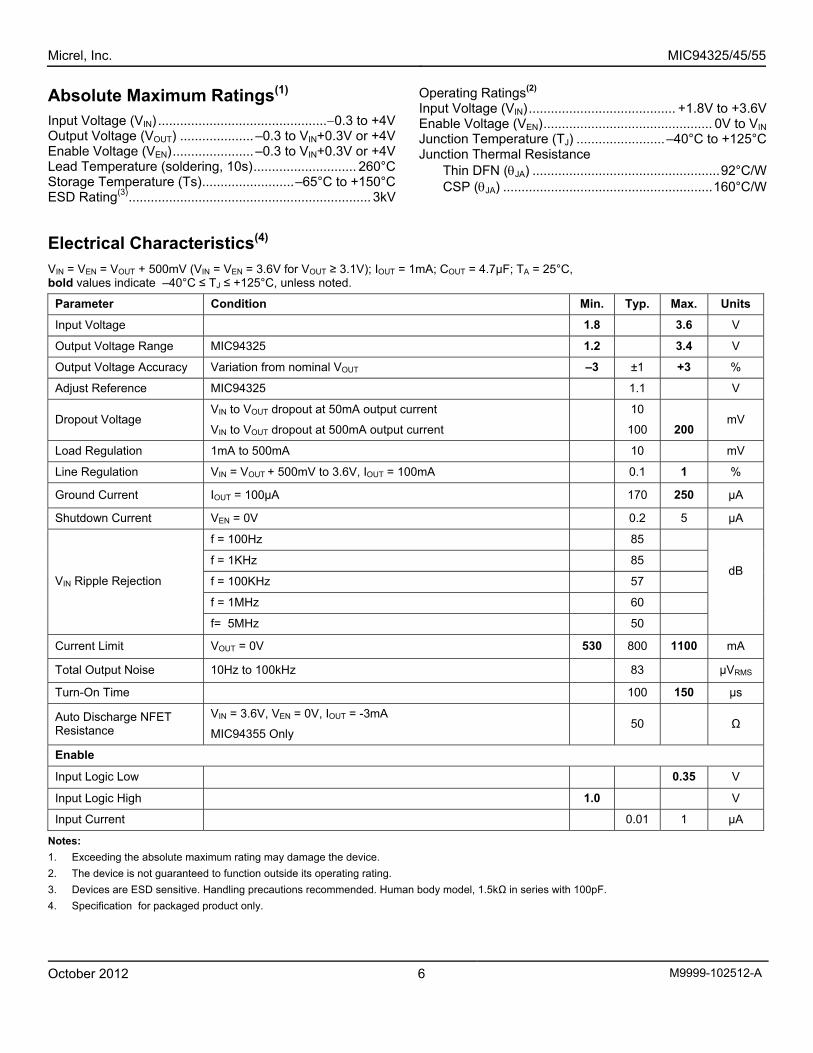
Absolute Maximum Ratings(1) Input Voltage (VIN) ..............................................0.3 to +4V Output Voltage (VOUT) .................... –0.3 to VIN+0.3V or +4V Enable Voltage (VEN)...................... –0.3 to VIN+0.3V or +4V Lead Temperature (soldering, 10s)............................ 260°C Storage Temperature (Ts).........................–65°C to +150°C ESD Rating(3).................................................................. 3kV
Operating Ratings(2) Input Voltage (VIN)........................................ +1.8V to +3.6V Enable Voltage (VEN).............................................. 0V to VIN Junction Temperature (TJ) ........................–40°C to +125°C Junction Thermal Resistance Thin DFN (JA) ...................................................92°C/W
Electrical Characteristics(4) VIN = VEN = VOUT + 500mV (VIN = VEN = 3.6V for VOUT ≥ 3.1V); IOUT = 1mA; COUT = 4.7µF; TA = 25°C, bold values indicate –40°C ≤ TJ ≤ +125°C, unless noted.
Parameter Condition Min. Typ. Max. Units
Input Voltage 1.8 3.6 V
Output Voltage Range MIC94325 1.2 3.4 V
Output Voltage Accuracy Variation from nominal VOUT –3 ±1 +3 %
Adjust Reference MIC94325 1.1 V
Dropout Voltage VIN to VOUT dropout at 50mA output current
VIN to VOUT dropout at 500mA output current
10
100
200 mV
Load Regulation 1mA to 500mA 10 mV
Line Regulation VIN = VOUT + 500mV to 3.6V, IOUT = 100mA 0.1 1 %
Ground Current IOUT = 100µA 170 250 µA
Shutdown Current VEN = 0V 0.2 5 µA
f = 100Hz 85
f = 1KHz 85
f = 100KHz 57
f = 1MHz 60
VIN Ripple Rejection
f= 5MHz 50
dB
Current Limit VOUT = 0V 530 800 1100 mA
Total Output Noise 10Hz to 100kHz 83 μVRMS
Turn-On Time 100 150 μs
Auto Discharge NFET Resistance
VIN = 3.6V, VEN = 0V, IOUT = -3mA
MIC94355 Only 50 Ω
Enable
Input Logic Low 0.35 V
Input Logic High 1.0 V
Input Current 0.01 1 µA
Notes:
1. Exceeding the absolute maximum rating may damage the device.
2. The device is not guaranteed to function outside its operating rating.
3. Devices are ESD sensitive. Handling precautions recommended. Human body model, 1.5kΩ in series with 100pF.
4. Specification for packaged product only.
Micrel, Inc. MIC94325/45/55
October 2012 7 M9999-102512-A
Typical Characteristics
MIC94325 PSRR COUT = 4.7µF CFF = 3.3nF
-120
-110
-100
-90
-80
-70
-60
-50
-40
-30
-20
10 100 1,000 10,000 100,000
1,000,000
10,000,000
FREQUENCY (Hz)
PS
RR
(d
B)
VIN = 2.7V + 40mvpp
VOUT = 2.2V
COUT = 4.7µF
CFF = 3.3nF
500mA
10 100 1K 10K 100K 1M 10M
300mA
10mA
MIC94325 PSRR COUT = 4.7µF , CFF = 10nF
-120
-110
-100
-90
-80
-70
-60
-50
-40
-30
-20
1.00E+01 1.00E+03 1.00E+05 1.00E+07FREQUENCY (Hz)
PS
RR
(d
B)
VIN = 2.4V + 40mvpp
VOUT = 2.2V
COUT = 4.7µF
CFF = 10nF
500mA
10mA
10 100 1K 10K 100K 1M 10M
300mA
MIC94325 PSRR COUT = 4.7µF , CFF = 10nF
-120
-110
-100
-90
-80
-70
-60
-50
-40
-30
-20
10 100 1,000 10,000 100,000
1,000,000
10,000,000
FREQUENCY (Hz)
PS
RR
(d
B)
VIN = 2.7V + 40mvpp
VOUT = 2.2V
COUT = 4.7µF
CFF = 10nF
500mA
10mA
10 100 1K 10K 100K 1M 10M
300mA
MIC94355 PSRRCOUT = 4.7µF
-120
-100
-80
-60
-40
-20
0
10 100 1,000 10,000 100,000
1,000,000
10,000,000
FREQUENCY (Hz)
PS
RR
(d
B)
VIN = 2.5V + 40mvpp
VOUT = 1.8V
COUT = 4.7µF
10 100 1K 10K 100K 1M 10M
200mA
500mA
10mA
MIC94325 PSRR COUT = 4.7µF CFF = 100nF
-120
-110
-100
-90
-80
-70
-60
-50
-40
-30
-20
10 100 1,000 10,000 100,000
1,000,000
10,000,000
FREQUENCY (Hz)
PS
RR
(d
B)
VIN = 2.7V + 40mvpp
VOUT = 2.2V
COUT = 4.7µF
CFF = 100nF
10 100 1K 10K 100K 1M 10M
500mA
300mA
10mA
MIC94355 PSRR COUT = 4.7µF
-120
-100
-80
-60
-40
-20
0
10 100 1,000 10,000 100,000
1,000,000
10,000,000
FREQUENCY (Hz)
PS
RR
(d
B)
VIN = 2.8V + 40mVpp
VOUT = 1.8V
COUT = 4.7µF
10 100 1K 10K 100K 1M 10M
10mA
200mA
500mA
MIC94355 PSRR COUT = 10µF
-120
-100
-80
-60
-40
-20
0
10 100 1,000 10,000 100,000
1,000,000
10,000,000
FREQUENCY (Hz)
PS
RR
(d
B)
VIN = 2.5V + 40mVpp
VOUT = 1.8V
COUT = 10µF
1K 10K 100K 1M 10M10 100
10mA
200mA500mA
MIC94355 PSRR COUT = 10µF
-120
-100
-80
-60
-40
-20
0
10 100 1,000 10,000 100,000
1,000,000
10,000,000
FREQUENCY(Hz)
PS
RR
(d
B)
VIN = 2.8V + 40mVpp
VOUT = 1.8V
COUT = 10µF
500mA
200mA
1K 10K 100K 1M 10M10 100
10mA
MIC34355 PSRR COUT = 4.7µF
-120
-100
-80
-60
-40
-20
0
10 100 1,000 10,000 100,000
1,000,000
10,000,000
FREQUENCY (Hz)
PS
RR
(d
B)
VIN = 3.6V + 40mVpp
VOUT = 1.8V
COUT = 4.7µF
10mA
200mA
1K 10K 100K 1M 10M10 100
500mA
Micrel, Inc. MIC94325/45/55
October 2012 8 M9999-102512-A
Typical Characteristics (Continued)
Output Voltage
vs. Output Current
1.6
1.65
1.7
1.75
1.8
1.85
1.9
1.95
2
0 50 100 150 200 250 300 350 400 450 500
OUTPUT CURRENT (mA)
OU
TP
UT
VO
LT
AG
E (
V)
VIN = 2.8V
CIN = COUT = 4.7µF
Ground Current vs. Output Current
150
155
160
165
170
175
180
185
190
195
200
0 50 100 150 200 250 300 350 400 450 500
OUTPUT CURRENT (mA)
GR
OU
ND
CU
RR
EN
T (
µA
)
MIC94355YMT
Output Noise Spectral Density
0.001
0.01
0.1
1
10
10 100 1,000 10,000 100,000
1,000,000
10,000,000
FREQUENCY (Hz)
MO
ISE
µV
/√H
zVIN = VEN = 3V
COUT = 4.7µF/10V
1K 10K 100K 1M 10M10 100
MIC94355 PSRR COUT = 10µF
-120
-100
-80
-60
-40
-20
0
10 100 1,000 10,000 100,000
1,000,000
10,000,000
FREQUENCY (Hz)
PS
RR
(d
B)
VIN = 3.6V + 40mVpp
VOUT = 1.8V
COUT = 10µF
100mA
1K 10K 100K 1M 10M10 100
10mA
200mA
Dropout Voltage vs. Load
0
10
20
30
40
50
60
70
80
90
100
0 50 100 150 200 250 300 350 400 450 500
LOAD (mA)
DR
OP
OU
T V
OL
TA
GE
(m
V)
VOUT = 1.8V
CIN = COUT = 4.7µF
Ground Current vs. Input Voltage
120
130
140
150
160
170
180
190
200
210
220
1.8 2 2.2 2.4 2.6 2.8 3 3.2 3.4 3.6
INPUT VOLTAGE (V)
GR
OU
ND
CU
RR
EN
T (
µA
)
500mA
50mA
CIN = COUT = 1µF
300mA
100mA
Micrel, Inc. MIC94325/45/55
October 2012 9 M9999-102512-A
Functional Characteristics
Micrel, Inc. MIC94325/45/55
October 2012 10 M9999-102512-A
Application Information The MIC943x5 family of products is a very-high PSRR, fixed-output, 500mA LDO utilizing Ripple Blocker technology. The MIC943x5 is fully protected from damage due to fault conditions, offering linear current limiting and thermal shutdown.
Input Capacitor
The MIC943x5 is a high-performance, high-bandwidth device. An input capacitor of 4.7µF is required from the input to ground to provide stability. Low-ESR ceramic capacitors provide optimal performance at a minimum of space. Additional high-frequency capacitors, such as small-valued NPO dielectric-type capacitors, help filter out high-frequency noise and are good practice in any RF-based circuit. X5R or X7R dielectrics are recommended for the input capacitor. Y5V dielectrics lose most of their capacitance over temperature and are therefore, not recommended.
Output Capacitor
In order to maintain stability, the MIC943x5 requires an output capacitor of 4.7µF or greater. For optimal input voltage ripple rejection performance a 4.7µF capacitor is recommended. The design is optimized for use with low-ESR ceramic chip capacitors. High-ESR capacitors are not recommended because they may cause high-frequency oscillation. The output capacitor can be increased, but performance has been optimized for a 4.7µF ceramic output capacitor and does not improve significantly with larger capacitance.
X7R/X5R dielectric type ceramic capacitors are recommended because of their temperature performance. X7R type capacitors change capacitance by 15% over their operating temperature range and are the most stable type of ceramic capacitors. Z5U and Y5V dielectric capacitors change their value by as much as 50% and 60%, respectively, over their operating temperature ranges. To use a ceramic chip capacitor with the Y5V dielectric, the value must be much higher than an X7R ceramic capacitor to ensure the same minimum capacitance over the equivalent operating temperature range.
No Load Stability
The MIC943x5 will remain stable and in regulation with no load. This is especially important in CMOS RAM keep-alive applications.
Enable/Shutdown
Forcing the enable (EN) pin low disables the MIC943x5 and sends it into a “zero” off mode current state. In this state, current consumed by the MIC943x5 goes nearly to zero. Forcing EN high enables the output voltage. The EN pin uses CMOS technology and cannot be left floating as it could cause an indeterminate state on the output.
For the MIC94325 adjustable part, the turn-on time is affected by the selection of the external feedback resistors and feed-forward capacitor. The relationship is approximately 2.2 x R2 x Cff, where R2 is the bottom resistor (connected from ADJ to GND) and Cff is the capacitor connected across R1 (from VOUT to ADJ). For stability, the feed-forward capacitor must be greater than 1nF. 10nF is recommended for best performance.
When disabled, the MIC94355 switches a 50Ω (typical) load on the regulator output to discharge the external capacitors.
Adjustable Regulator Application
The MIC94325 output voltage can be adjusted by using two external resistors (Figure 1). The resistors set the output voltage based on the following equation:
R2
R11VV ADJOUT
VADJ = 1.1V
Figure 1. Adjustable Output Voltage
Thermal Considerations
The MIC943x5 is designed to provide 500mA of continuous current in a very-small package. Maximum ambient operating temperature can be calculated based on the output current and the voltage drop across the part. For example if the input voltage is 2.5V, the output voltage is 1.8V, and the output current = 500mA. The actual power dissipation of the Ripple Blocker™ can be determined using the equation:
Micrel, Inc. MIC94325/45/55
October 2012 11 M9999-102512-A
PD = (VIN – VOUT1) I OUT + VIN IGND For more information about Micrel’s Ripple Blocker products, go to:
Because this device is CMOS and the ground current is typically <170µA over the load range, the power dissipation contributed by the ground current is <1% and can be ignored for this calculation.
TJ(max) = 125°C, the maximum junction temperature of the
die, θJA thermal resistance = 160°C/W for the YCS package and 92°C/W for the Thin DFN package.
Substituting PD for PD(MAX) and solving for the ambient operating temperature will give the maximum operating conditions for the regulator circuit.
The maximum power dissipation must not be exceeded for proper operation.
For example, when operating the MIC94325-GYMT at an input voltage of 2.5V and 500mA load with a minimum footprint layout, the maximum ambient operating temperature TA can be determined as follows:
0.35W = (125°C – TA)/(92°C/W)
TA = 92°C
Therefore, the maximum ambient operating temperature allowed in a 1.6mm x 1.6mm Thin DFN package is 92°C. For a full discussion of heat sinking and thermal effects on voltage regulators, refer to the “Regulator Thermals” section of Micrel’s Designing with Low-Dropout Voltage Regulators handbook. This information can be found on Micrel's website at:
MICREL, INC. 2180 FORTUNE DRIVE SAN JOSE, CA 95131 USA TEL +1 (408) 944-0800 FAX +1 (408) 474-1000 WEB http://www.micrel.com
Micrel makes no representations or warranties with respect to the accuracy or completeness of the information furnished in this data sheet. This
information is not intended as a warranty and Micrel does not assume responsibility for its use. Micrel reserves the right to change circuitry, specifications and descriptions at any time without notice. No license, whether express, implied, arising by estoppel or otherwise, to any intellectual
property rights is granted by this document. Except as provided in Micrel’s terms and conditions of sale for such products, Micrel assumes no liability whatsoever, and Micrel disclaims any express or implied warranty relating to the sale and/or use of Micrel products including liability or warranties
relating to fitness for a particular purpose, merchantability, or infringement of any patent, copyright or other intellectual property right.
Micrel Products are not designed or authorized for use as components in life support appliances, devices or systems where malfunction of a product reasonably be expected to result in personal injury. Life support devices or systems are devices or systems that (a) are intended for surgical implainto the body or (b) support or sustain life, and whose failure to perform can be reasonably expected to result in a significant injury to the user. A
Purchaser’s use or sale of Micrel Products for use in life support appliances, devices or systems is a Purchaser’s own risk and Purchaser agrees to fully indemnify Micrel for any damages resulting from such use or sale.