23
55GHz Octal-site Wafer Test Probecard for 5G mmWave devices Jason Mroczkowski Director of R&D Cohu
55GHz Octal-site Wafer Test Probecard for 5G mmWave devices
Jason MroczkowskiDirector of R&D
Cohu

Intro: 5G mmWave Drivers• Demand
– Urban area capacity, fixed wireless broadband (FWA), video streaming, AR/VR, Critical IOT such as autonomous vehicles and mobile healthcare
• Frequency– 5G FR2 (frequency range 2) (24.25GHz to 52.6GHz)– Bandwidth up to 3.4GHz
• 5G Comparison:– 5G sub-6Ghz 200Mb/s– 5G mmWave 5Gb/s
• Percentage mmWave sales– 43% phones by 2022
2Jason Mroczkowski
www.5gmmwave.com/5g-mmwave/5g-mmwave-nsa-or-sa/
https://www.macrumors.com/guide/mmwave-vs-sub-6ghz-5g/
200
5000
5G sub-6 5G mmWave
Mb/
s
Speed Comparison
7.00%
25.00%
43.00%
2020 2021 2022
% mmWave 5G Sales
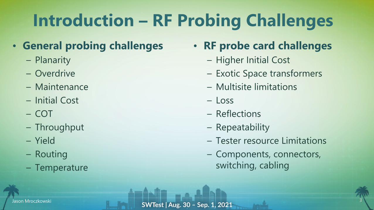
Introduction – RF Probing Challenges• General probing challenges
– Planarity– Overdrive– Maintenance– Initial Cost– COT– Throughput– Yield– Routing– Temperature
• RF probe card challenges – Higher Initial Cost– Exotic Space transformers– Multisite limitations– Loss– Reflections– Repeatability– Tester resource Limitations– Components, connectors,
switching, cabling
3Jason Mroczkowski

WLCSP Objectives / Goals• Mechanical targets
– 600+ i/o die– 150um pitch– Octal Site Probecard– ~5000 contacts– <50um planarity – >100 RF connectors/cables– >100 01005 components
(capacitors, resistors)– >80 RF mmWave switches– Full probecard including stiffener,
cabling, docking, RF brackets, etc.
• Electrical targets– 55GHz to tester – 55Ghz loopback– 44GHz switching– Low impedance power supplies– -10dB max return loss – 50ohm impedance match– Simulated and measured full path
from tester to DUT for calibration and de-embedding
4Jason Mroczkowski

Methods/Materials• cRacer Probehead
– 3mm test height spring probe, 150um pitch, 6g, 150um overdrive (DUT side)
– Metal frame, stiffener, 8 site MA– Simulated and optimized signal integrity,
bowing/stress analysis– Measured life cycle, cRes, CCC, RF, planarity,
force• Direct Attach PCB
– Fanout in PCB (no space transformer/MLO/MLC required)
– 100+ RF channels (5GHz-55GHz RF paths)• Simulated signal integrity (HFSS, SI Wave)• DUT side: surface, internal• Tester side: surface, internal
– 25 Power supplies• Simulated IR drop and impedance (SI Wave) all 8
sites
• Connectors/Cabling– SMPM connectors, Cabling
• Simulated launch geometries• Switching
– 44GHz dual pole switches – Simulated launch geometries
• Components– 01005 capacitors and resistors for
signal integrity and space savings– Simulated footprints
• Simulation and Measurement equipment– Ansys CFD, HFSS, SI Wave– PCA (Cohu FReD machine) – VNA (67GHz Keysight)– Cycler (Kita)
Jason Mroczkowski 5
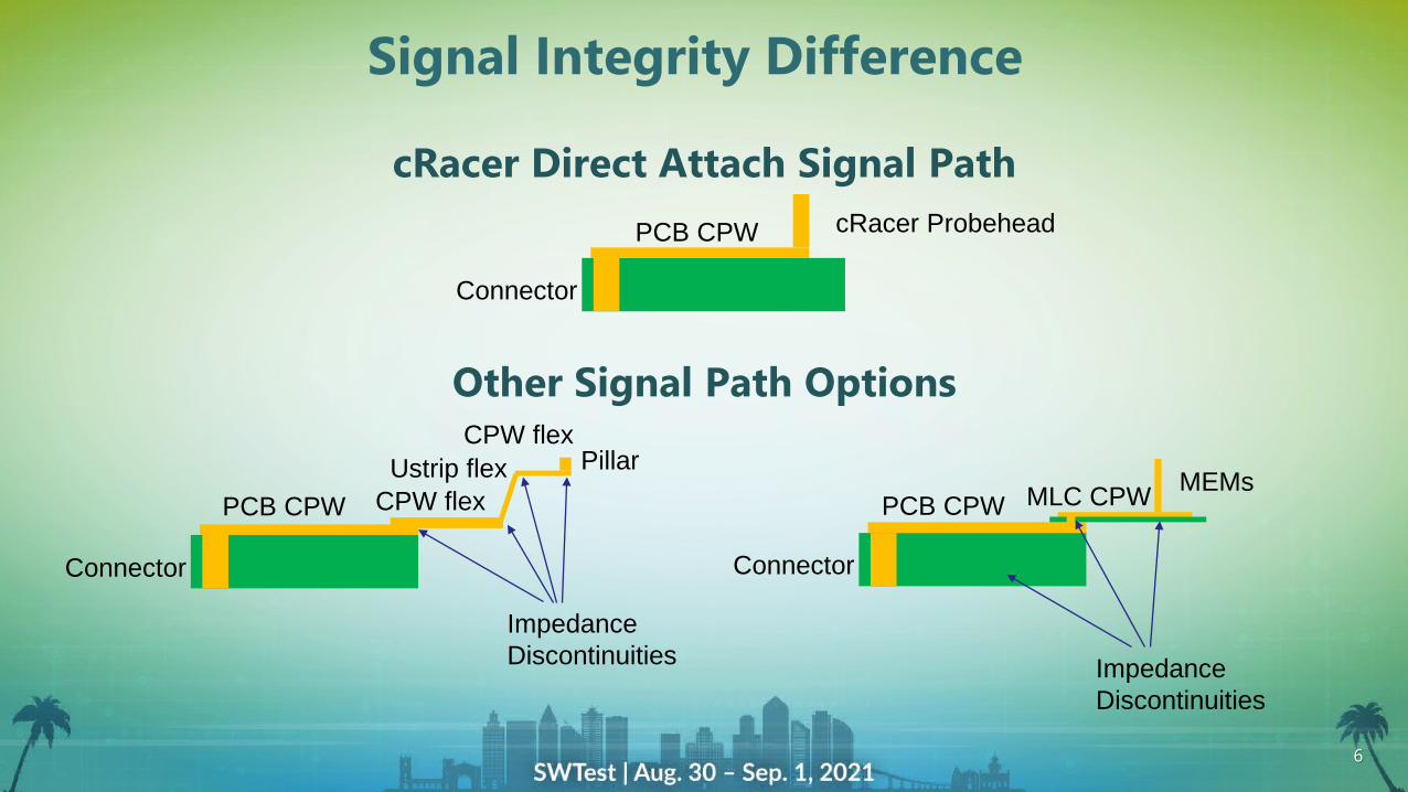
cRacer Direct Attach Signal Path
Other Signal Path Options
Signal Integrity Difference
PCB CPW cRacer Probehead
Connector
PCB CPWUstrip flex
CPW flex
CPW flexPillar
Impedance Discontinuities
Connector
PCB CPWMEMs
Connector
Impedance Discontinuities
MLC CPW
6
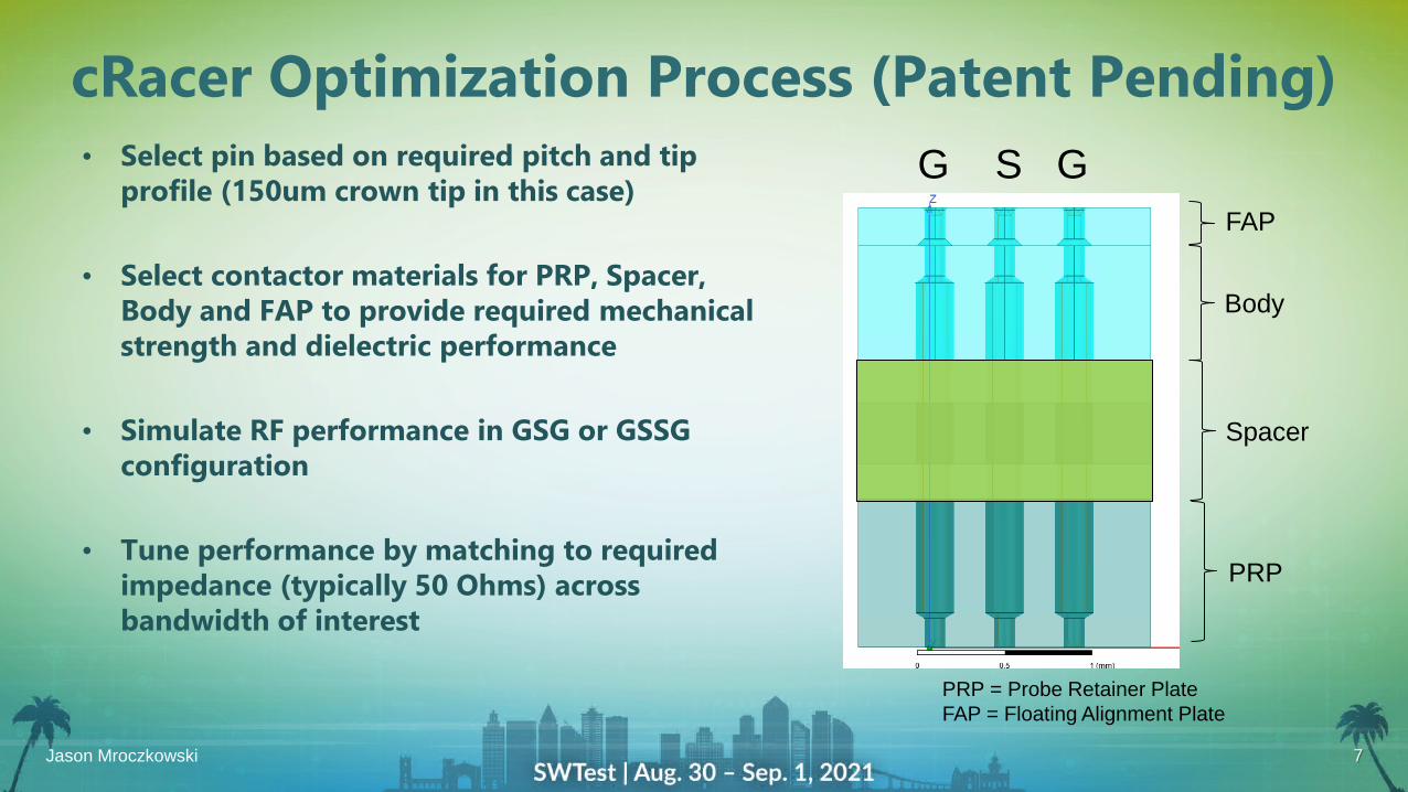
cRacer Optimization Process (Patent Pending)• Select pin based on required pitch and tip
profile (150um crown tip in this case)
• Select contactor materials for PRP, Spacer, Body and FAP to provide required mechanical strength and dielectric performance
• Simulate RF performance in GSG or GSSG configuration
• Tune performance by matching to required impedance (typically 50 Ohms) across bandwidth of interest
PRP = Probe Retainer Plate FAP = Floating Alignment Plate
G S G
PRP
Spacer
Body
FAP
Jason Mroczkowski 7
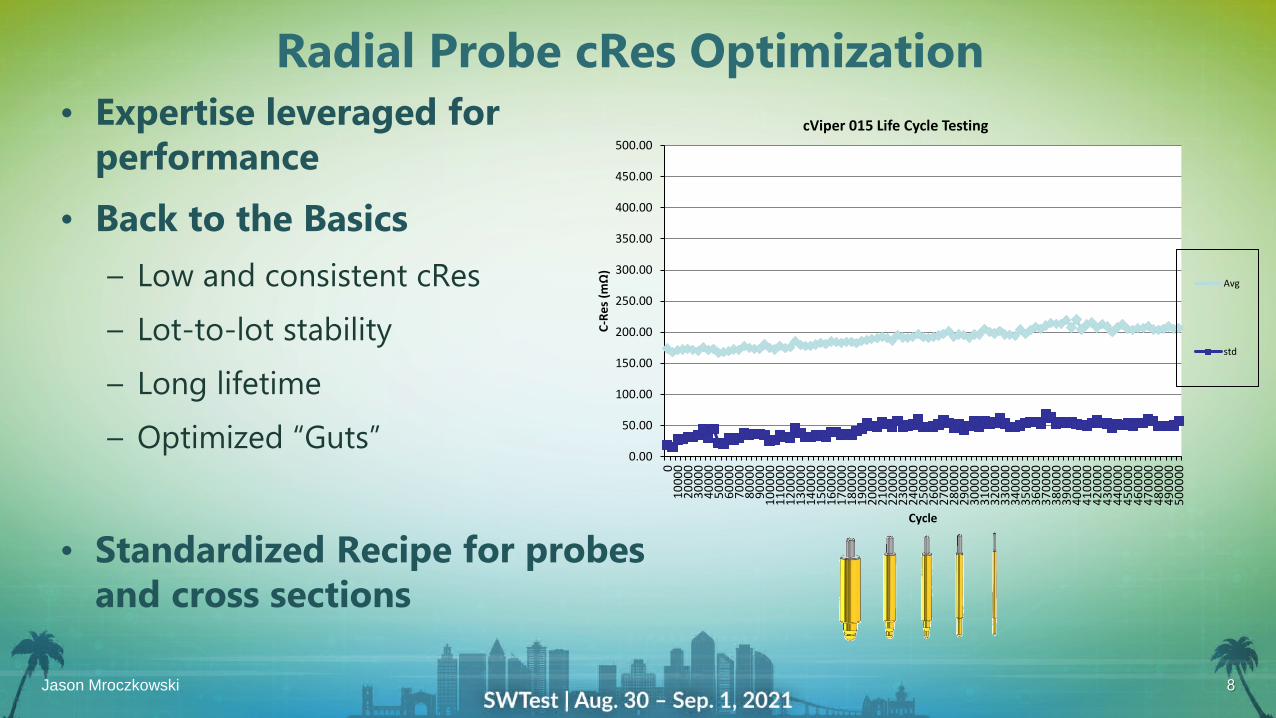
• Expertise leveraged for performance
• Back to the Basics– Low and consistent cRes– Lot-to-lot stability– Long lifetime– Optimized “Guts”
• Standardized Recipe for probes and cross sections
Radial Probe cRes Optimization
0.00
50.00
100.00
150.00
200.00
250.00
300.00
350.00
400.00
450.00
500.00
010
000
2000
030
000
4000
050
000
6000
070
000
8000
090
000
1000
0011
0000
1200
0013
0000
1400
0015
0000
1600
0017
0000
1800
0019
0000
2000
0021
0000
2200
0023
0000
2400
0025
0000
2600
0027
0000
2800
0029
0000
3000
0031
0000
3200
0033
0000
3400
0035
0000
3600
0037
0000
3800
0039
0000
4000
0041
0000
4200
0043
0000
4400
0045
0000
4600
0047
0000
4800
0049
0000
5000
00
C-Re
s (m
Ω)
Cycle
cViper 015 Life Cycle Testing
Avg
std
Jason Mroczkowski 8

• Predict the bowing deflection due to probe preload that can be expected from Probehead using Ansys simulation
• Max Y-Directional Deformation: 10.3 µm
Bowing Simulation – Rev 04
Jason Mroczkowski 9

cRacer Probehead Simulated Insertion Loss• Predict the insertion loss and return loss expected from Probehead using Ansys simulation
out to 55GHz– Great performance with <1dB Insertion loss, <-12dB return loss through 60GHz
G S G
Jason Mroczkowski 10
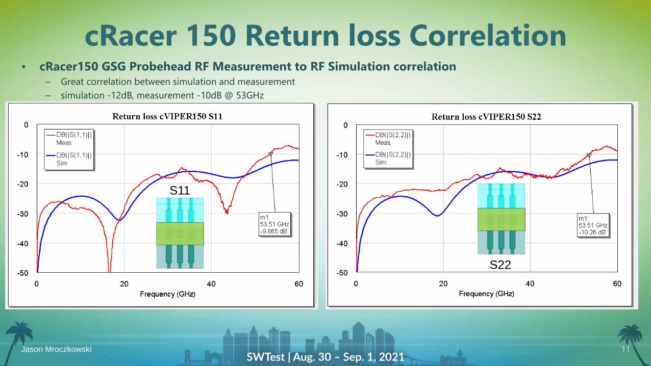
cRacer 150 Return loss Correlation • cRacer150 GSG Probehead RF Measurement to RF Simulation correlation
– Great correlation between simulation and measurement– simulation -12dB, measurement -10dB @ 53GHz
••
S22
S11
Jason Mroczkowski 11

• High return loss found for mmWave signals on device• Alternative materials attempted• Impedance is still too low (approx. 40Ω)
– Recommended Solution - > De-Populate the 3rd GND Probe in the Probehead
– Return loss before -7dB, Return loss after -12dB
RL issue for mmWave signals
G S G
G
Jason Mroczkowski 12
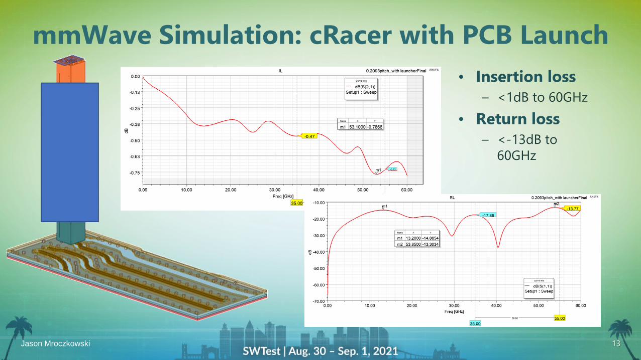
mmWave Simulation: cRacer with PCB Launch• Insertion loss
– <1dB to 60GHz• Return loss
– <-13dB to 60GHz
Jason Mroczkowski 13

• Current Density • Voltage Drop
DC Simulations (1V supply)
Target IR drop less than 24mV (16mV Max simulated) achieved thru Ansys SI Wave simulation
Jason Mroczkowski 14
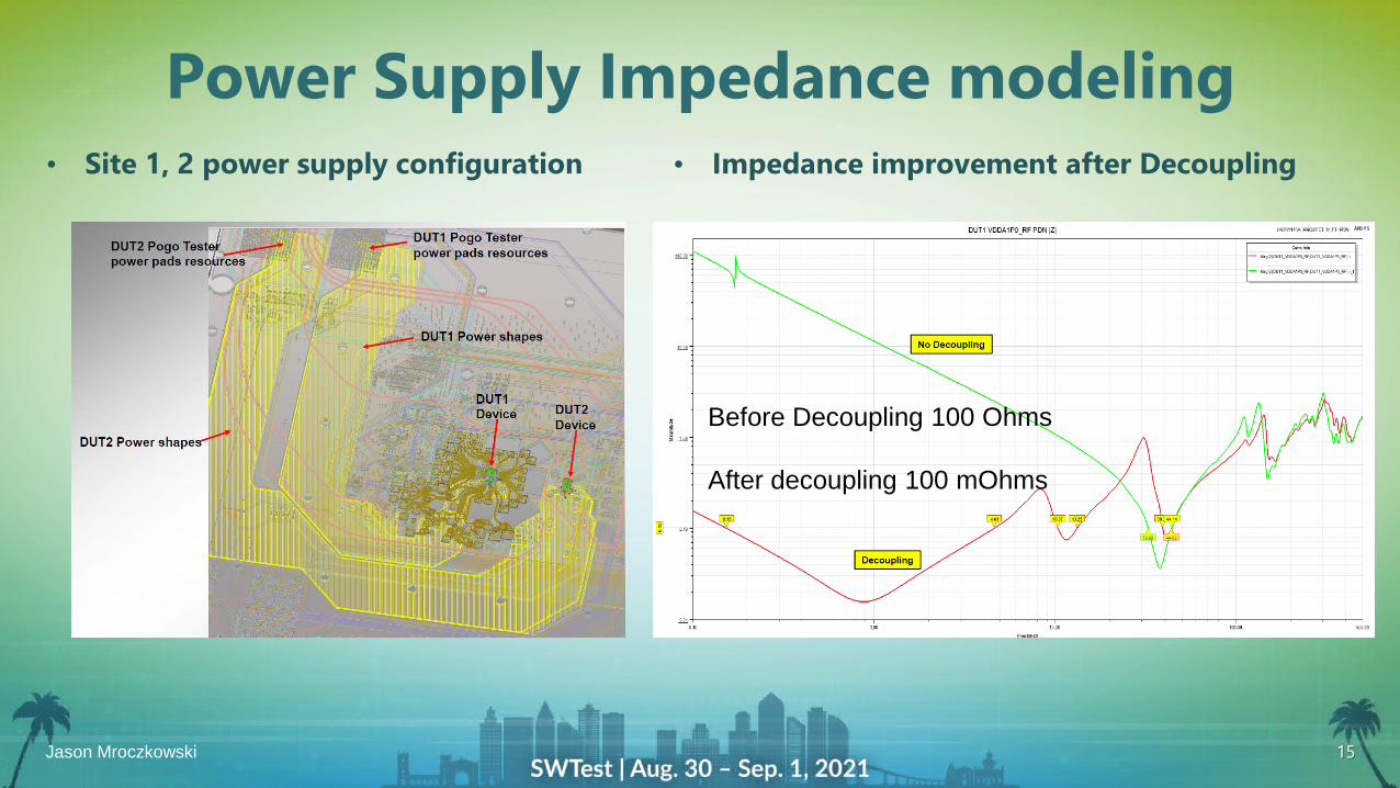
Power Supply Impedance modeling• Site 1, 2 power supply configuration • Impedance improvement after Decoupling
Before Decoupling 100 Ohms
After decoupling 100 mOhms
Jason Mroczkowski 15
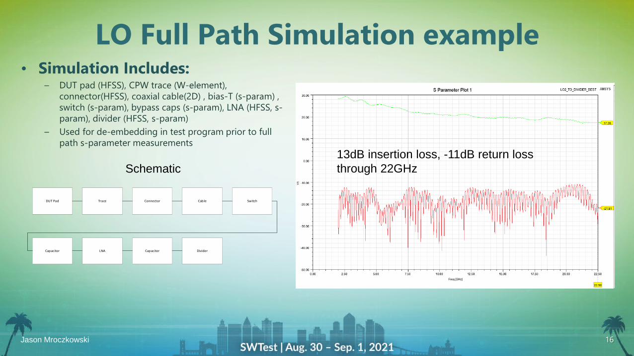
LO Full Path Simulation example• Simulation Includes:
– DUT pad (HFSS), CPW trace (W-element), connector(HFSS), coaxial cable(2D) , bias-T (s-param) , switch (s-param), bypass caps (s-param), LNA (HFSS, s-param), divider (HFSS, s-param)
– Used for de-embedding in test program prior to full path s-parameter measurements
16
13dB insertion loss, -11dB return loss through 22GHz
Jason Mroczkowski
Schematic
DUT Pad Trace Connector
Capacitor LNA
Cable Switch
Capacitor Divider

• Tester to DUT full path loss (qty12 55GHz paths)– Return loss below -10dB and linear insertion loss thru 55GHz– Includes contactor, vias, traces, connector, 18” coax cable
Full Path S-parameter measurment to 55GHz
Jason Mroczkowski 17
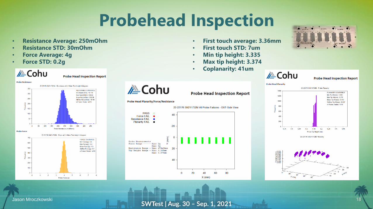
Probehead Inspection• Resistance Average: 250mOhm• Resistance STD: 30mOhm• Force Average: 4g• Force STD: 0.2g
• First touch average: 3.36mm• First touch STD: 7um• Min tip height: 3.335• Max tip height: 3.374 • Coplanarity: 41um
Jason Mroczkowski 18
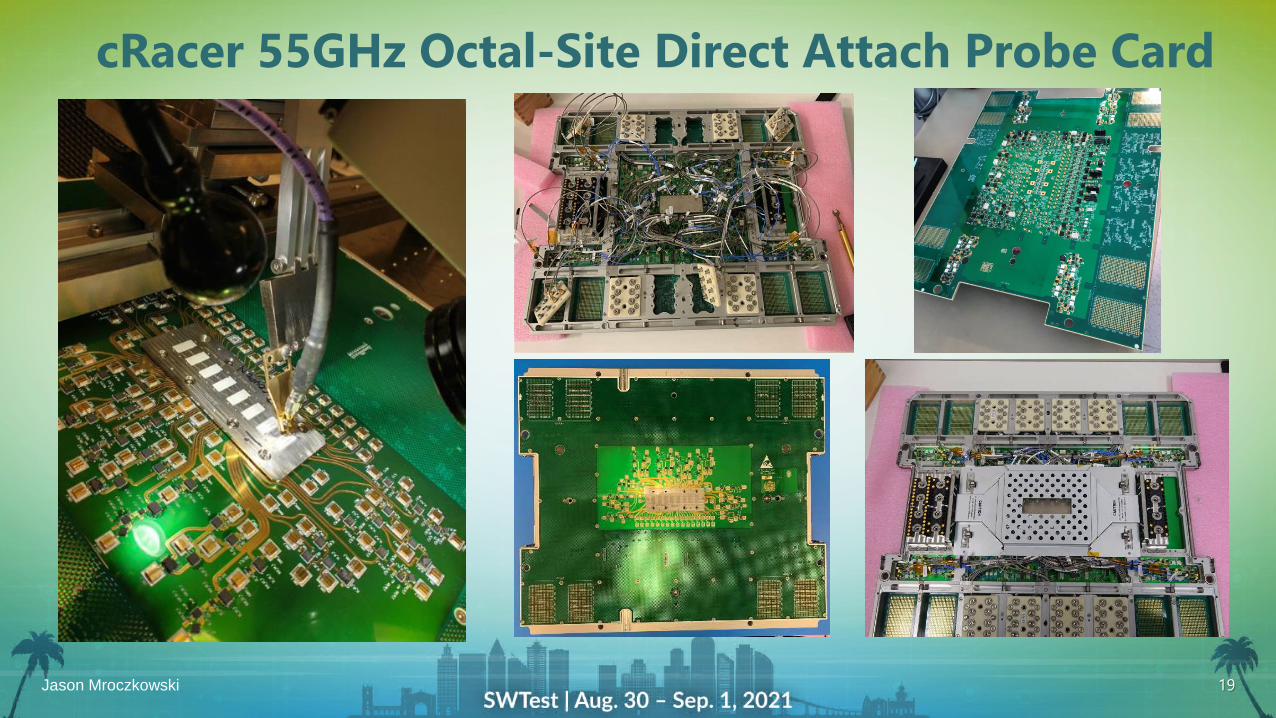
cRacer 55GHz Octal-Site Direct Attach Probe Card
Jason Mroczkowski 19

Discussion of Results• Advantages
– 8+ site capable mmWave Probecard Solution– Traditional Spring Probe Technology– Direct Attach (no MLO/MLC)– Field maintainable– Lower Cost of Test
• Challenges– Significant Engineering Design effort– Limited real-estate limits optimal RF Routing– Complex PCB stackup– High BOM count/cost and assembly complexity– Long-leadtime mmWave components
20Jason Mroczkowski
Summary / Conclusion• Proven performance and parallelism of a cRacer
probehead+Direct attach PCB for up to mmWave and down to 150um pitch– Turnkey Production Probe solution for any RF application from DC
to Daylight• Design, Simulation, Prototype and Final build efforts to
deliver– Required mechanical and electrical expertise, supply chain
management, assembly and test coordination, and logistics management to get the job done right the first time
21Jason Mroczkowski

Follow-On Work• Redesign for alternative impedance profile• Optimize cable lengths and routing for lower loss• Improve manual actuator for singulated die testing• Simplify logistics for High Volume Deliveries
22Jason Mroczkowski
Thanks to:• Synergie CAD
– Mahmoud Mesgarzadeh (Design Team Manager)– John Holmes (PCB CAD Engineer)– Paul Holland (RF Simulation Engineer)
• Cohu– Aaren Lonks (RF Product Development Manager)– Peter Cockburn (Senior Product Marketing Manager)– Anne Krantz (Product Development Engineering Manager)
23Jason Mroczkowski


