Page 1
7/21/2019 55LA860V, 860W, 868V, 8609
http://slidepdf.com/reader/full/55la860v-860w-868v-8609 1/127
CHASSIS : LD34D
MODEL: 55LA86** 55LA86**-Z*
CAUTIONBEFORE SERVICING THE CHASSIS,
READ THE SAFETY PRECAUTIONS IN THIS MANUAL.
LED TV
SERVICE MANUAL
North/Latin America http://aic.lgservice.com
Europe/Africa http://eic.lgservice.com
Asia/Oceania http://biz.lgservice.com
Internal Use Only
Page 2
7/21/2019 55LA860V, 860W, 868V, 8609
http://slidepdf.com/reader/full/55la860v-860w-868v-8609 2/127
CONTENTS
CONTENTS .............................................................................................. 2
SAFETY PRECAUTIONS ........................................................................ 3
SERVICING PRECAUTIONS .................................................................... 4
SPECIFICATION ....................................................................................... 6
ADJUSTMENT INSTRUCTION .............................................................. 13
EXPLODED VIEW .................................................................................. 23
SCHEMATIC CIRCUIT DIAGRAM ..............................................................
Page 3
7/21/2019 55LA860V, 860W, 868V, 8609
http://slidepdf.com/reader/full/55la860v-860w-868v-8609 3/127
Many electrical and mechanical parts in this chassis have special safety-related characteristics. These parts are identified by in the
Schematic Diagram and Exploded View.
It is essential that these special safety parts should be replaced with the same components as recommended in this manual to prevent
Shock, Fire, or other Hazards.
Do not modify the original design without permission of manufacturer.
General Guidance
An isolation Transformer should always be used during theservicing of a receiver whose chassis is not isolated from the AC
power line. Use a transformer of adequate power rating as this
protects the technician from accidents resulting in personal injury
from electrical shocks.
It will also protect the receiver and it's components from being
damaged by accidental shorts of the circuitry that may be
inadvertently introduced during the service operation.
If any fuse (or Fusible Resistor) in this TV receiver is blown,replace it with the specified.
When replacing a high wattage resistor (Oxide Metal Film Resistor,
over 1 W), keep the resistor 10 mm away from PCB.
Keep wires away from high voltage or high temperature parts.
Before returning the receiver to the customer,
l f AC l k t h k th d
Leakage Current Hot Check (See below Figure)
Plug the AC cord directly into the AC outlet.
Do not use a line Isolation Transformer during this check.
Connect 1.5 K / 10 watt resistor in parallel with a 0.15 uF capacitor
between a known good earth ground (Water Pipe, Conduit, etc.)
and the exposed metallic parts.
Measure the AC voltage across the resistor using AC voltmeter
with 1000 ohms/volt or more sensitivity.
Reverse plug the AC cord into the AC outlet and repeat AC voltage
measurements for each exposed metallic part. Any voltage
measured must not exceed 0.75 volt RMS which is corresponds to
0.5 mA.In case any measurement is out of the limits specified, there is
possibility of shock hazard and the set must be checked and
repaired before it is returned to the customer.
Leakage Current Hot Check circuit
IMPORTANT SAFETY NOTICE
SAFETY PRECAUTIONS
Page 4
7/21/2019 55LA860V, 860W, 868V, 8609
http://slidepdf.com/reader/full/55la860v-860w-868v-8609 4/127
SERVICING PRECAUTIONS
CAUTION: Before servicing receivers covered by this service
manual and its supplements and addenda, read and follow the
SAFETY PRECAUTIONS on page 3 of this publication.NOTE : If unforeseen circumstances create conict between the
following servicing precautions and any of the safety precautions
on page 3 of this publication, always follow the safety precau-
tions. Remember: Safety First.
General Servicing Precautions
1. Always unplug the receiver AC power cord from the AC power
source before;
a. Removing or reinstalling any component, circuit board
module or any other receiver assembly.
b. Disconnecting or reconnecting any receiver electrical plug
or other electrical connection.
c. Connecting a test substitute in parallel with an electrolytic
capacitor in the receiver.
CAUTION: A wrong part substitution or incorrect polarity
installation of electrolytic capacitors may result in an explo-
sion hazard.
2. Test high voltage only by measuring it with an appropriate
high voltage meter or other voltage measuring device (DVM,
FETVOM, etc) equipped with a suitable high voltage probe.
Do not test high voltage by "drawing an arc".3. Do not spray chemicals on or near this receiver or any of its
assemblies.
4. Unless specied otherwise in this service manual, clean
electrical contacts only by applying the following mixture to the
contacts with a pipe cleaner, cotton-tipped stick or comparable
non-abrasive applicator; 10 % (by volume) Acetone and 90 %
(by volume) isopropyl alcohol (90 % - 99 % strength)
CAUTION: This is a ammable mixture.
Unless specied otherwise in this service manual, lubrication
of contacts in not req ired
2. After removing an electrical assembly equipped with ES
devices, place the assembly on a conductive surface such as
aluminum foil, to prevent electrostatic charge buildup or expo-sure of the assembly.
3. Use only a grounded-tip soldering iron to solder or unsolder
ES devices.
4. Use only an anti-static type solder removal device. Some sol-
der removal devices not classied as “anti-static” can generate
electrical charges sufcient to damage ES devices.
5. Do not use freon-propelled chemicals. These can generate
electrical charges sufcient to damage ES devices.
6. Do not remove a replacement ES device from its protective
package until immediately before you are ready to install it.
(Most replacement ES devices are packaged with leads elec-
trically shorted together by conductive foam, aluminum foil or
comparable conductive material).
7. Immediately before removing the protective material from the
leads of a replacement ES device, touch the protective mate-
rial to the chassis or circuit assembly into which the device will
be installed.
CAUTION: Be sure no power is applied to the chassis or cir-
cuit, and observe all other safety precautions.
8. Minimize bodily motions when handling unpackaged replace-
ment ES devices. (Otherwise harmless motion such as thebrushing together of your clothes fabric or the lifting of your
foot from a carpeted oor can generate static electricity suf-
cient to damage an ES device.)
General Soldering Guidelines
1. Use a grounded-tip, low-wattage soldering iron and appropri-
ate tip size and shape that will maintain tip temperature within
the range or 500 °F to 600 °F.
2. Use an appropriate gauge of RMA resin-core solder composed
of 60 parts tin/40 parts lead
Page 5
7/21/2019 55LA860V, 860W, 868V, 8609
http://slidepdf.com/reader/full/55la860v-860w-868v-8609 5/127
IC Remove/Replacement
Some chassis circuit boards have slotted holes (oblong) through
which the IC leads are inserted and then bent at against the cir-cuit foil. When holes are the slotted type, the following technique
should be used to remove and replace the IC. When working with
boards using the familiar round hole, use the standard technique
as outlined in paragraphs 5 and 6 above.
Removal
1. Desolder and straighten each IC lead in one operation by
gently prying up on the lead with the soldering iron tip as the
solder melts.
2. Draw away the melted solder with an anti-static suction-type
solder removal device (or with solder braid) before removing
the IC.Replacement
1. Carefully insert the replacement IC in the circuit board.
2. Carefully bend each IC lead against the circuit foil pad and
solder it.
3. Clean the soldered areas with a small wire-bristle brush.
(It is not necessary to reapply acrylic coating to the areas).
"Small-Signal" Discrete Transistor
Removal/Replacement1. Remove the defective transistor by clipping its leads as close
as possible to the component body.
2. Bend into a "U" shape the end of each of three leads remain-
ing on the circuit board.
3. Bend into a "U" shape the replacement transistor leads.
4. Connect the replacement transistor leads to the corresponding
leads extending from the circuit board and crimp the "U" with
long nose pliers to insure metal to metal contact then solder
each connection.
3. Solder the connections.
CAUTION: Maintain original spacing between the replaced
component and adjacent components and the circuit board toprevent excessive component temperatures.
Circuit Board Foil Repair
Excessive heat applied to the copper foil of any printed circuit
board will weaken the adhesive that bonds the foil to the circuit
board causing the foil to separate from or "lift-off" the board. The
following guidelines and procedures should be followed when-
ever this condition is encountered.
At IC Connections
To repair a defective copper pattern at IC connections use the
following procedure to install a jumper wire on the copper pattern
side of the circuit board. (Use this technique only on IC connec-
tions).
1. Carefully remove the damaged copper pattern with a sharp
knife. (Remove only as much copper as absolutely necessary).
2. carefully scratch away the solder resist and acrylic coating (if
used) from the end of the remaining copper pattern.
3. Bend a small "U" in one end of a small gauge jumper wire and
carefully crimp it around the IC pin. Solder the IC connection.4. Route the jumper wire along the path of the out-away copper
pattern and let it overlap the previously scraped end of the
good copper pattern. Solder the overlapped area and clip off
any excess jumper wire.
At Other Connections
Use the following technique to repair the defective copper pattern
at connections other than IC Pins. This technique involves the
installation of a jumper wire on the component side of the circuit
board
Page 6
7/21/2019 55LA860V, 860W, 868V, 8609
http://slidepdf.com/reader/full/55la860v-860w-868v-8609 6/127
SPECIFICATIONNOTE : Specifications and others are subject to change without notice for improvement.
1. Application rangeThis specification is applied to the LED TV used LD34D
chassis.
2. Requirement for TestEach part is tested as below without special appointment.
1) Temperature: 25 °C ± 5 °C(77 °F ± 9 °F), CST: 40 °C ± 5 °C
2) Relative Humidity: 65 % ± 10 %
3) Power Voltage
: Standard input voltage (AC 100-240 V~, 50/60 Hz)* Standard Voltage of each products is marked by models.
4) Specification and performance of each parts are followed
each drawing and specification by part number in
accordance with BOM.
5) The receiver must be operated for about 20 minutes prior to
the adjustment.
3. Test method1) Performance: LGE TV test method followed
2) Demanded other specification
- Safety : CE, IEC specification
- EMC : CE, IEC
- Wireless : Wireless HD Specification (Option)
4. Model General Specification
No. Item Specication Remarks
DTV & Analog (Total 37 countries)
DTV (MPEG2/4, DVB-T) : 30 countries
Germany, Netherland, Switzerland, Hungary, Austria, Slovenia, Bul-
garia, France, Spain, Italy, Belgium, Russia, Luxemburg, Greece,
Czech, Croatia, Turkey, Moroco, Ireland, Latvia, Estonia, Lithuania,
Poland, Portugal, Romania, Albania, Bosnia, Serbia, Slovakia, Be-
ralus
Page 7
7/21/2019 55LA860V, 860W, 868V, 8609
http://slidepdf.com/reader/full/55la860v-860w-868v-8609 7/127
No. Item Specication Remarks
2 Broadcasting system 1) PAL-BG/DK/I/I’
2) SECAM L/L’, DK, BG, I
3) DVB-T/T2, C, S/S2
3 Program coverage
1 ) Digital TV
- VHF, UHF
- C-Band, Ku-Band
2) Analogue TV
-VHF : E2 to E12
-UHF : E21 to E69
-CATV : S1 to S20
-HYPER : S21 to S47
4 Receiving system
Analog : Upper Heterodyne
Digital : COFDM, QAM
► DVB-T
- Guard Interval(Bitrate_Mbit/s)
1/4, 1/8, 1/16, 1/32
- Modulation : Code Rate
QPSK : 1/2, 2/3, 3/4, 5/6, 7/8
16-QAM : 1/2, 2/3, 3/4, 5/6, 7/8
64-QAM : 1/2, 2/3, 3/4, 5/6, 7/8
► DVB-T2
- Guard Interval(Bitrate_Mbit/s)
1/4, 1/8, 1/16, 1/32, 1/128, 19/128, 19/256,- Modulation : Code Rate
QPSK : 1/2, 2/5, 2/3, 3/4, 5/6
16-QAM : 1/2, 2/5, 2/3, 3/4, 5/6
64-QAM : 1/2, 2/5, 2/3, 3/4, 5/6
256-QAM : 1/2, 2/5, 2/3, 3/4, 5/6
► DVB-C
- Symbolrate : 4.0Msymbols/s to 7.2 Msymbols/s
- Modulation : 16QAM, 64-QAM, 128-QAM and 256-QAM
Page 8
7/21/2019 55LA860V, 860W, 868V, 8609
http://slidepdf.com/reader/full/55la860v-860w-868v-8609 8/127
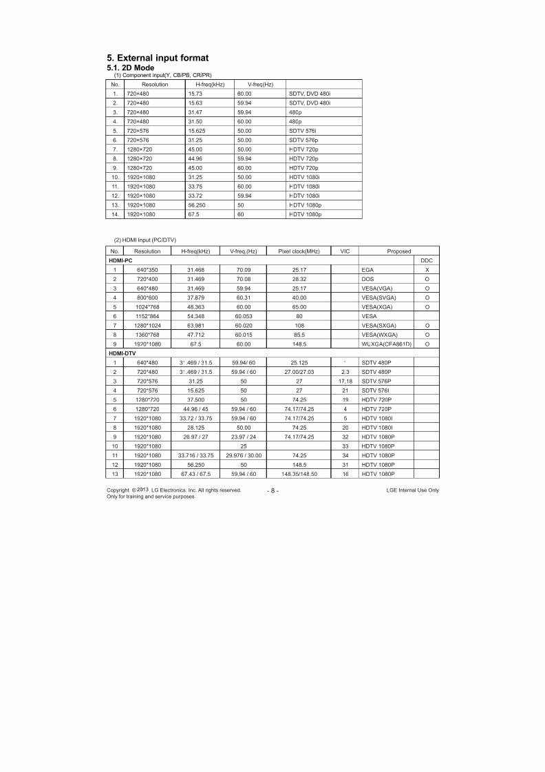
5. External input format
5.1. 2D Mode(1) Component input(Y, CB/PB, CR/PR)
(2) HDMI Input (PC/DTV)
No. Resolution H-freq(kHz) V-freq(Hz)
1. 720×480 15.73 60.00 SDTV, DVD 480i
2. 720×480 15.63 59.94 SDTV, DVD 480i
3. 720×480 31.47 59.94 480p
4. 720×480 31.50 60.00 480p
5. 720×576 15.625 50.00 SDTV 576i
6. 720×576 31.25 50.00 SDTV 576p7. 1280×720 45.00 50.00 HDTV 720p
8. 1280×720 44.96 59.94 HDTV 720p
9. 1280×720 45.00 60.00 HDTV 720p
10. 1920×1080 31.25 50.00 HDTV 1080i
11. 1920×1080 33.75 60.00 HDTV 1080i
12. 1920×1080 33.72 59.94 HDTV 1080i
13. 1920×1080 56.250 50 HDTV 1080p
14. 1920×1080 67.5 60 HDTV 1080p
No. Resolution H-freq(kHz) V-freq.(Hz) Pixel clock(MHz) VIC Proposed
HDMI-PC DDC
1 640*350 31.468 70.09 25.17 EGA Х
Page 9
7/21/2019 55LA860V, 860W, 868V, 8609
http://slidepdf.com/reader/full/55la860v-860w-868v-8609 9/127
5.2. 3D Mode(1) RF Input(3D supported mode manually)
No. Resolution Proposed 3D input proposed mode
1 HD - DTV1080I
720P 2D to 3D
Side by Side(Half)
Top & Bottom2 SD - DTV
576P
576I
3 SD - ATV(CVBS/SCART)
(3) HDMI 1.3 (3D supported mode manually)
No Resolution H-freq(kHz) V-freq.(Hz) Pixel clock(MHz) Proposed 3D input proposed mode
1 720*480 31.5 60 27.03 SDTV 480P
2D to 3D, Side by Side(Half), Top & Bottom,
Checker Board, Frame Sequential, Row
Interleaving, Column Interleaving
2 720*576 31.25 50 27 SDTV 576P
3 1280*720 45.00 60.00 74.25 HDTV 720P
4 1280*720 37.500 50 74.25 HDTV 720P
5 1920*1080 33 75 60 00 74 25 HDTV 1080I
(2) RF Input(3D supported mode automatically)
No. Signal 3D input proposed mode
1 Frame CompatibleSide by Side(Half),
Top & Bottom
Page 10
7/21/2019 55LA860V, 860W, 868V, 8609
http://slidepdf.com/reader/full/55la860v-860w-868v-8609 10/127
(4) HDMI 1.4b (3D supported mode automatically)
No. Resolution H-freq(kHz) V-freq.(Hz) Pixel clock(MHz) VIC 3D input proposed mode Proposed
1
640*480
31.469 / 31.5 59.94/ 60 25.125/25.2 1 Top-and-BottomSide-by-side(half)
Secondary(SDTV 480P)Secondary(SDTV 480P)
2 62.938/63 59.94/ 60 50.35/50.4 1Frame packing
Line alternative
Secondary(SDTV 480P)
(SDTV 480P)
3 31.469 / 31.5 59.94/ 60 50.35/50.4 1 Side-by-side(Full) (SDTV 480P)
4
720*480
31.469 / 31.5 59.94 / 60 27.00/27.03 2,3Top-and-Bottom
Side-by-side(half)
Secondary(SDTV 480P)
Secondary(SDTV 480P)
5 62.938/63 59.94 / 60 54/54.06 2,3Frame packing
Line alternative
Secondary(SDTV 480P)
(SDTV 480P)
6 31.469 / 31.5 59.94 / 60 54/54.06 2,3 Side-by-side(Full) (SDTV 480P)
7
720*576
31.25 50 27 17,18Top-and-BottomSide-by-side(half)
Secondary(SDTV 576P)Secondary(SDTV 576P)
8 62.5 50 54 17,18Frame packing
Line alternative
Secondary(SDTV 576P)
(SDTV 576P)
9 31.25 50 54 17,18 Side-by-side(Full) (SDTV 576P)
10
1280*720
37.500 50 74.25 19Top-and-Bottom
Side-by-side(half)
Primary(HDTV 720P)
Primary(HDTV 720P)
11 75 50 148.5 19Frame packing
Field alternative
Primary(HDTV 720P)
(HDTV 720P)
12 37.500 50 148.5 19 Side-by-side(Full) (HDTV 720P)
13 44.96 / 45 59.94 / 60 74.18/74.25 4Top-and-BottomSide-by-side(half)
Primary(HDTV 720P)Primary(HDTV 720P)
14 89.91/90 59.94 / 60 148.35/148.5 4Frame packing
Line alternative
Primary(HDTV 720P)
(HDTV 720P)
15 44.96 / 45 59.94 / 60 148.35/148.5 4 Side-by-side(Full) (HDTV 720P)
16 33.72 / 33.75 59.94 / 60 74.18/74.25 5Top-and-Bottom
Side-by-side(half)
Secondary(HDTV 1080I)
Primary(HDTV 1080I)
17 67.432/67.50 59.94 / 60 148.35/148.5 5Frame packing
Line alternative
Primary(HDTV 1080I)
(HDTV 1080I)
18 33 72 / 33 75 59 94 / 60 148 35/148 5 5 Side by side(Full) (HDTV 1080I)
Page 11
7/21/2019 55LA860V, 860W, 868V, 8609
http://slidepdf.com/reader/full/55la860v-860w-868v-8609 11/127
No. Resolution H-freq(kHz) V-freq.(Hz) Pixel clock(MHz) 3D input proposed mode Proposed
1 1024*768 48.36 60 652D to 3D, Side by Side(half)
Top & BottomHDTV 768P
2 1360*768 47.71 60 85.52D to 3D, Side by Side(half)
Top & BottomHDTV 768P
3 1920*1080 67.500 60 148.50
2D to 3D, Side by Side(half)
Top & Bottom, Checker Board,
Single Frame Sequential,
Row Interleaving,
Column Interleaving
HDTV 1080P
4 Others - - - 2D to 3D
640*350720*400
640*480
800*600
1152*864
(5) HDMI-PC Input (3D) (3D supported mode manually)
(6) Component Input ( 3D) (3D supported mode manually)
No. Resolution H-freq(kHz) V-freq.(Hz) Pixel clock 3D input proposed mode Proposed
1 1280*720 37.5 50 74.25 2D to 3D, Side by Side, Top & Bottom HDTV 720P
2 1280*720 45.00 60.00 74.25 2D to 3D, Side by Side, Top & Bottom HDTV 720P
3 1280*720 44.96 59.94 74.176 2D to 3D, Side by Side, Top & Bottom HDTV 720P
4 1920*1080 33.75 60.00 74.25 2D to 3D, Side by Side, Top & Bottom HDTV 1080I
5 1920*1080 33.72 59.94 74.176 2D to 3D, Side by Side, Top & Bottom HDTV 1080I
6 1920*1080 28.12 50 74.25 2D to 3D, Side by Side, Top & Bottom HDTV 1080I
7 1920*1080 67.500 60 148.50 2D to 3D, Side by Side, Top & Bottom HDTV 1080P
Page 12
7/21/2019 55LA860V, 860W, 868V, 8609
http://slidepdf.com/reader/full/55la860v-860w-868v-8609 12/127
No. Resolution H-freq(kHz) V-freq.(Hz) Pixel clock(MHz) 3D input proposed mode
1 Under 704x480 2D to 3D
2Over 704x480
interlaced2D to 3D, Side by Side(Half), Top & Bottom
3Over 704x480
progressive
50 / 602D to 3D, Side by Side(Half), Top & Bottom, Checker Board,
Row Interleaving, Column Interleaving, Frame Sequential
4 others2D to 3D, Side by Side(Half), Top & Bottom, Checker Board,
Row Interleaving, Column Interleaving
(7) USB, DLNA – Movie (3D) (3D supported mode manually)
(9) USB, DLNA (3D) (3D supported mode automatically)
No. Resolution H-freq(kHz) V-freq.(Hz) Pixel clock(MHz) 3D input proposed mode
1 Under 320x240 - - - 2D to 3D
2 Over 320x240 - - - 2D to 3D, Side by Side(Half), Top & Bottom
(8) USB, DLNA -Photo (3D) (3D supported mode manually)
No. Resolution H-freq(kHz) V-freq.(Hz) Pixel clock(MHz) 3D input proposed mode
1 1080p 33.75 30 74.25Side by Side(Half), Top & Bottom, Checker
Board, MPO(Photo), JPS(Photo)
■ Remark: 3D Input mode
No Side by Side Top & Bottom Checker boardSingle Frame Frame Line Column
2D to 3D
Page 13
7/21/2019 55LA860V, 860W, 868V, 8609
http://slidepdf.com/reader/full/55la860v-860w-868v-8609 13/127
ADJUSTMENT INSTRUCTION
1. Application RangeThis specification sheet is applied to all of the LED TV with
LD34D chassis.
2. Designation(1) Because this is not a hot chassis, it is not necessary to
use an isolation transformer. However, the use of isolation
transformer will help protect test instrument.
(2) Adjustment must be done in the correct order.
(3) The adjustment must be performed in the circumstance of
25 °C ± 5 °C of temperature and 65 % ± 10 % of relative
humidity if there is no specific designation.(4) The input voltage of the receiver must keep AC 100-240
V~, 50/60 Hz.
(5) The receiver must be operated for about 5 minutes prior to
the adjustment when module is in the circumstance of over
15.
In case of keeping module is in the circumstance of 0 °C, it
should be placed in the circumstance of above 15 °C for 2
hours.
In case of keeping module is in the circumstance of below
-20 °C, it should be placed in the circumstance of above 15
°C for 3 hours.
[Caution]
When still image is displayed for a period of 20 minutes or
longer (Especially where W/B scale is strong. Digital pattern
13ch and/or Cross hatch pattern 09ch), there can some
afterimage in the black level area.
3.1.3. Adjustment(1) Adjustment method
- Using RS-232, adjust items in the other shown in"3.1.3.3)"
(2) Adj. protocol
Ref.) ADC Adj. RS232C Protocol_Ver1.0
(3) Adj. order - aa 00 00 [Enter ADC adj. mode]
- xb 00 04 [Change input source to Component1 (480i&
1080p)]
- ad 00 10 [Adjust 480i&1080p Comp1]
- xb 00 06 [Change input source to RGB(1024*768)]
- ad 00 10 [Adjust 1920*1080 SCART RGB]
- ad 00 90 End adj.
3.2. MAC address D/L, CI+ key D/L, Widevine
Protocol Command Set ACK
Enter adj. mode aa 00 00 a 00 OK00x
Source changexb 00 04
xb 00 06
b 00 OK04x (Adjust 480i, 1080p Comp1 )
b 00 OK06x (Adjust 1920*1080 SCART RGB)
Begin adj. ad 00 10
Return adj. resultOKx (Case of Success)
NGx (Case of Fail)
Read adj. data
(main)ad 00 20
(main)000000000000000000000000007c007b006dx
(sub )
ad 00 21
(Sub)
000000070000000000000000007c00830077x
Conrm adj. ad 00 99
NG 03 00x (Fail)
NG 03 01x (Fail)NG 03 02x (Fail)
OK 03 03x (Success)
End adj. aa 00 90 a 00 OK90x
Page 14
7/21/2019 55LA860V, 860W, 868V, 8609
http://slidepdf.com/reader/full/55la860v-860w-868v-8609 14/127
3.3. LAN Inspection3.3.1. Equipment & Condition
▪ Each other connection to LAN Port of IP Hub and Jig
3.3.2. LAN inspection solution▪ LAN Port connection with PCB
▪ Network setting at MENU Mode of TV
▪ Setting automatic IP
▪ Setting state confirmation
→ If automatic setting is finished, you confirm IP and MAC
Address.
3.3.3. WIDEVINE key Inspection
3.4. LAN PORT INSPECTION(PING TEST)Connect SET → LAN port == PC → LAN Port
3.4.1. Equipment setting(1) Play the LAN Port Test PROGRAM.
(2) Input IP set up for an inspection to Test Program.
*IP Number : 12.12.2.2
3.4.2. LAN PORT inspection(PING TEST)(1) Play the LAN Port Test Program.
(2) Connect each other LAN Port Jack.(3) Play Test (F9) button and confirm OK Message.
(4) Remove LAN cable.
SET PC
Page 15
7/21/2019 55LA860V, 860W, 868V, 8609
http://slidepdf.com/reader/full/55la860v-860w-868v-8609 15/127
3.6. Model name & Serial number Download3.6.1. Model name & Serial number D/L
▪ Press "Power on" key of service remote control.(Baud rate : 115200 bps)
▪ Connect RS-232C Signal to USB Cable to USB.
▪ Write Serial number by use USB port.
▪ Must check the serial number at Instart menu.
3.6.2. Method & notice(1) Serial number D/L is using of scan equipment.
(2) Setting of scan equipment operated by Manufacturing
Technology Group.
(3) Serial number D/L must be conformed when it is producedin production line, because serial number D/L is mandatory
by D-book 4.0.
* Manual Download (Model Name and Serial Number)
If the TV set is downloaded by OTA or service man, sometimes
model name or serial number is initialized.(Not always)
It is impossible to download by bar code scan, so It need
Manual download.
1) Press the "Instart" key of Adjustment remote control.
2) Go to the menu "7.Model Number D/L" like below photo.
3) Input the Factory model name(ex 47LM960V-ZB) or Serialnumber like photo.
2) Check the key download for transmitted command
(RS232: ci 00 10)
3) Result value
- Normally status for download : OKx
- Abnormally status for download : NGx
3.7.2. Check the method of CI+ key value(RS232)1) Into the main ass’y mode(RS232: aa 00 00)
2) Check the mothed of CI+ key by command
(RS232: ci 00 20)
3) Result value
i 01 OK 1d1852d21c1ed5dcx
3.8. WIFI MAC ADDRESS CHECK(1) Using RS232 Command
H-freq(kHz) V-freq.(Hz)
Transmission [A][I][][Set ID][][20][Cr] [O][K][X] or [NG]
CMD 1 CMD 2 Data 0C I 1 0
CMD 1 CMD 2 Data 0 A A 0 0
CMD 1 CMD 2 Data 0
C I 2 0
CI+ Key Value
Page 16
7/21/2019 55LA860V, 860W, 868V, 8609
http://slidepdf.com/reader/full/55la860v-860w-868v-8609 16/127
4. Manual Adjustment* ADC adjustment is not needed because of OTP(Auto ADC
adjustment)
4.1. EDID(The Extended Display Identification
Data)/DDC(Display Data Channel) download4.1.1. Overview
It is a VESA regulation. A PC or a MNT will display an optimal
resolution through information sharing without any necessity
of user input. It is a realization of "Plug and Play".
4.1.2. Equipment
- Since embedded EDID data is used, EDID download JIG,HDMI cable and D-sub cable are not need.
- Adjustment remote control
4.1.3. Download method(1) Press "ADJ" key on the Adjustment remote control then
select "10.EDID D/L", By pressing "Enter" key, enter EDID
D/L menu.
(2) Select "Start" button by pressing "Enter" key, HDMI1/
HDMI2/ HDMI3/ HDMI4/ RGB are writing and display OK
or NG.
ⓓ Model Name(Hex): LGTV
Cf) TV set’s model name in EDID data is below.
ⓔ Checksum(LG TV): Changeable by total EDID data.
ⓕ Vendor Specific(HDMI)
(1) EDID
# HDMI 1(C/S : E8 81)
EDID Block 0, Bytes 0-127 [00H-7FH]
EDID Block 1, Bytes 128-255 [80H-FFH]
For HDMI EDID
DVI-D to HDMI or HDMI to HDMI
0 1 2 3 4 5 6 7 8 9 A B C D E F
00 00 FF FF FF FF FF FF 00 1E 6D 01 00 01 01 01 01
10 01 17 01 03 80 A0 5A 78 0A EE 91 A3 54 4C 99 2620 0F 50 54 A1 08 00 31 40 45 40 61 40 71 40 81 80
30 01 01 01 01 01 01 02 3A 80 18 71 38 2D 40 58 2C
40 45 00 40 84 63 00 00 1E 66 21 50 B0 51 00 1B 30
50 40 70 36 00 40 84 63 00 00 1E 00 00 00 FD 00 3A
60 3E 1E 53 10 00 0A 20 20 20 20 20 20 00 00 00 FC
70 00 4C 47 20 54 56 0A 20 20 20 20 20 20 20 01 E8
0 1 2 3 4 5 6 7 8 9 A B C D E F
80 02 03 3A F1 4E 10 9F 04 13 05 14 03 02 12 20 21
MODEL NAME MODEL NAME(HEX)
LG TV 00 00 00 FC 00 4C 47 20 54 56 0A 20 20 20 20 20 20 20 (LG TV)
EDID C/S dataFHD
HDMI
check sum (Hex)
Block 0 42
Block 123 (HDMI1)
13 (HDMI2)
INPUT MODEL NAME(HEX)
HDMI1 78030C001000801E
HDMI2 78030C002000801E
Page 17
7/21/2019 55LA860V, 860W, 868V, 8609
http://slidepdf.com/reader/full/55la860v-860w-868v-8609 17/127
# HDMI 3(C/S : E8 61)
EDID Block 0, Bytes 0-127 [00H-7FH]
EDID Block 1, Bytes 128-255 [80H-FFH]
# HDMI 4(C/S : E8 51) EDID Block 0, Bytes 0-127 [00H-7FH]
4.2.2. Equipment(1) Color Analyzer: CA-210 (LED Module : CH 14)
(2) Adjustment Computer(During auto adj., RS-232C protocolis needed)
(3) Adjustment Remote control
(4) Video Signal Generator MSPG-925F 720p/216-Gray
(Model: 217, Pattern: 78)
→ Only when internal pattern is not available
▪ Color Analyzer Matrix should be calibrated using CS-100.
4.2.3. Equipment connection MAP
4.2.4. Adj. Command (Protocol)<Command Format>
- LEN: Number of Data Byte to be sent
- CMD: Command
- VAL: FOS Data value
- CS: Checksum of sent data
- A: Acknowledge
Ex) [Send: JA_00_DD] / [Ack: A_00_okDDX]
▪ RS-232C Command used during auto-adjustment.
START 6E A 50 A LEN A 03 A CMD A 00 A VAL A CS STOP
Color Analyzer
Computer
Pattern Generator
RS-232C
RS-232C
RS-232C
Probe
Signal Source
* If TV internal pattern is used, not needed
RS-232C COMMANDExplantion
0 0 1 2 3 4 5 6 7 8 9 A B C D E F
00 00 FF FF FF FF FF FF 00 1E 6D 01 00 01 01 01 01
10 01 17 01 03 80 A0 5A 78 0A EE 91 A3 54 4C 99 26
20 0F 50 54 A1 08 00 31 40 45 40 61 40 71 40 81 80
30 01 01 01 01 01 01 02 3A 80 18 71 38 2D 40 58 2C
40 45 00 40 84 63 00 00 1E 66 21 50 B0 51 00 1B 30
50 40 70 36 00 40 84 63 00 00 1E 00 00 00 FD 00 3A
60 3E 1E 53 10 00 0A 20 20 20 20 20 20 00 00 00 FC
70 00 4C 47 20 54 56 0A 20 20 20 20 20 20 20 01 E8
0 0 1 2 3 4 5 6 7 8 9 A B C D E F
00 02 03 3A F1 4E 10 9F 04 13 05 14 03 02 12 20 21
10 22 15 01 29 3D 06 C0 15 07 50 09 57 07 78 03 0C
20 00 30 00 B8 2D 20 C0 0E 01 4F 3F FC 08 10 18 10
30 06 10 16 10 28 10 E3 05 03 01 02 3A 80 18 71 38
40 2D 40 58 2C 45 00 40 84 63 00 00 1E 01 1D 80 18
50 71 1C 16 20 58 2C 25 00 40 84 63 00 00 9E 01 1D
60 00 72 51 D0 1E 20 6E 28 55 00 40 84 63 00 00 1E
70 00 00 00 00 00 00 00 00 00 00 00 00 00 00 00 61
0 0 1 2 3 4 5 6 7 8 9 A B C D E F
00 00 FF FF FF FF FF FF 00 1E 6D 01 00 01 01 01 01
10 01 17 01 03 80 A0 5A 78 0A EE 91 A3 54 4C 99 26
20 0F 50 54 A1 08 00 31 40 45 40 61 40 71 40 81 80
30 01 01 01 01 01 01 02 3A 80 18 71 38 2D 40 58 2C
40 45 00 40 84 63 00 00 1E 66 21 50 B0 51 00 1B 30
50 40 70 36 00 40 84 63 00 00 1E 00 00 00 FD 00 3A
60 3E 1E 53 10 00 0A 20 20 20 20 20 20 00 00 00 FC
70 00 4C 47 20 54 56 0A 20 20 20 20 20 20 20 01 E8
Page 18
7/21/2019 55LA860V, 860W, 868V, 8609
http://slidepdf.com/reader/full/55la860v-860w-868v-8609 18/127
▪ Adj. Map
4.2.5. Adj. method(1) Auto adj. method
1) Set TV in adj. mode using POWER ON key.
2) Zero calibrate probe then place it on the center of the
Display.
3) Connect Cable.(RS-232C to USB)
4) Select mode in adj. Program and begin adj.
5) When adj. is complete (OK Sign), check adj. status pre
mode. (Warm, Medium, Cool)
) S C
* CASE Cool
First adjust the coordinate far away from the target
value(x, y).1. x, y > target
i) Decrease the R, G.
2. x, y < target
i) First decrease the B gain,
3. x > target, y < target
i) First decrease B, so make y a little more than the target.
ii) Adjust x value by decreasing the R
4. x < target, y > target
i) First decrease B, so make x a little more than the target.
ii) Adjust x value by decreasing the G
How to adjust
1. If G gain is adjusted over 172 and R gain and B gain
less than 192 , Adjust is O.K.
2. If G gain is less than 172 , increase G gain by up to
172, and then increase R gain and B gain same
amount of increasing G gain.
3. If R gain or B gain is over 255 , Readjust G gain less
than 172, Conform to R gain is 255 or B gain is 255
* CASE Medium / WarmFirst adjust the coordinate far away from the target
value(x, y).
1. x, y > target
i) Decrease the R, G.
2. x, y < target
i) First decrease the B gain,
ii) Decrease the one of the others.
3. x > target, y < target
i) First decrease B, so make y a little more than the target.
ii) Adj st al e b decreasing the R
Adj. itemCommand
(lower caseASCII)
Data Range
(Hex.)
Default
(Decimal)
CMD1 CMD2 MIN MAX
Cool
R Gain j g 00 C0
G Gain j h 00 C0
B Gain j i 00 C0
R Cut
G Cut
B Cut
Medium
R Gain j a 00 C0
G Gain j b 00 C0
B Gain j c 00 C0
R Cut
G Cut
B Cut
Warm
R Gain j d 00 C0
G Gain j e 00 C0
B Gain j f 00 C0
R Cut
G Cut
Page 19
7/21/2019 55LA860V, 860W, 868V, 8609
http://slidepdf.com/reader/full/55la860v-860w-868v-8609 19/127
▪ Standard color coordinate and temperature using CA-210(CH 18)
4.2.7. EDGE LED White balance table(1) EDGE LED module change color coordinate because of
aging time.
(2) Apply under the color coordinate table, for compensated
aging time.(3) Normal line(Edge)
- Gumi (Mar ~ Dec) & Global
(4) Aging Chamber(Edge)
4.3. Local Dimming Function CheckStep 1) Turn on TV.
Step 2) At the Local Dimming mode, module Edge Backlightmoving right to left Back light of IOP module moving.
Step 3) Confirm the Local Dimming mode.
Step 4) Press "exit" key.
4.4. Magic Motion Remote control test(1) Equipment : RF Remote control for test, IR-KEY-Code
Remote control for test
(2) You must confirm the battery power of RF-Remote control
before test(recommend that change the battery per every lot)(3) Sequence (test)
1) if you select the "Start(Mute)" key on the Adjustment
remote control, you can pairing with the TV SET.
2) You can check the cursor on the TV Screen, when select
the "OK" key on the Adjustment remote control.
3) You must remove the pairing with the TV Set by select
"OK" key + "Mute" key on the Adjustment remote control
for 5 seconds.
ModeCoordinate
Temp ∆uvx y
Cool 0.271±0.002 0.270±0.002 13000K 0.0000
Medium 0.285±0.002 0.293±0.002 9300K 0.0000
Warm 0.310±0.002 0.325±0.002 6500K 0.0000
GP4
Aging
time
(Min)
Cool Medium Warm
X y x y x y
271 270 285 293 313 329
1 0-2 281 287 295 310 320 342
2 3-5 280 285 294 308 319 340
3 6-9 278 284 292 307 317 339
4 10-19 276 281 290 304 315 3365 20-35 275 277 289 300 314 332
6 36-49 274 274 288 297 313 329
7 50-79 273 272 287 295 312 327
8 80-119 272 271 286 294 311 326
9 Over 120 271 270 285 293 310 325
Aging Cool Medium Warm
Page 20
7/21/2019 55LA860V, 860W, 868V, 8609
http://slidepdf.com/reader/full/55la860v-860w-868v-8609 20/127
4.6. Wi-Fi TestStep 1) Turn on TV
Step 2) Select Network Connection option in Network Menu.
Step 3) Select Start Connection button in Network Connection.
Step 4) If the system finds any AP like blow PIC, it is working
well.
4.8. Inspection of light scattering▪ Test Method
(1) Push “Power only” key.
(2) Push “HDMI” hot key.
(3) Inspect whether light scattering is occurred in internal
black pattern or not.(4) Push “Power only” key.
4.9. Option selection per country4.9.1. Overview
- Option selection is only done for models in Non-EU.
4.9.2. Method(1) Press ADJ key on the Adjustment Remote Control, then
l t C t G M
Page 21
7/21/2019 55LA860V, 860W, 868V, 8609
http://slidepdf.com/reader/full/55la860v-860w-868v-8609 21/127
4.11. HDMI ARC Function Inspection(1) Test equipment
- Optic Receiver Speaker - MSHG-600 (SW: 1220 ↑)
- HDMI Cable (for 1.4 version)
(2) Test method
1) Insert the HDMI Cable to the HDMI ARC port from the
master equipment (HDMI1)
2) Check the sound from the TV Set
3) Check the Sound from the Speaker or using AV & Optic
TEST program (It’s connected to MSHG-600)
4.13. Ship-out mode check(In-stop)▪ After final inspection, press "IN-STOP" key of the Adjustment
remote control and check that the unit goes to Stand-bymode.
4.14. Tool Option selection- Method: Press ADJ key on the Adj. R/C, then select Tool option.
4.15. GND and Internal Pressure check4.15.1. Method
(1) GND & Internal Pressure auto-check preparation
- Check that Power cord is fully inserted to the SET. (If loose, re-insert)
(2) Perform GND & Internal Pressure auto-check
- Unit fully inserted Power cord, Antenna cable and A/V
arrive to the auto-check process.
- Connect D-terminal to AV JACK TESTER
- Auto CONTROLLER(GWS103-4) ON
- Perform GND TEST
- If NG, Buzzer will sound to inform the operator.
- If OK, changeover to I/P check automatically.
(Remove CORD, A/V form AV JACK BOX.)
- Perform I/P test- If NG, Buzzer will sound to inform the operator.
- If OK, Good lamp will lit up and the stopper will allow the
pallet to move on to next process.
4.15.2. Checkpoint▪ TEST voltage
- GND: 1.5 KV / min at 100 mA
- SIGNAL: 3 KV / min at 100 mA
▪ TEST time: 1 second
Page 22
7/21/2019 55LA860V, 860W, 868V, 8609
http://slidepdf.com/reader/full/55la860v-860w-868v-8609 22/127
6. USB S/W Download(Service only)(1) Put the USB Stick to the USB socket.
(2) Automatically detecting update file in USB Stick.- If your downloaded program version in USB Stick is Low,
it didn't work. But your downloaded version is High, USB
data is automatically detecting.(Download Version High &
Power only mode, Set is automatically Download)
(3) Show the message "Copying files from memory".
(4) Updating is starting.
(5) Updating Completed, The TV will restart automatically.
(6) If your TV is turned on, check your updated version and
Tool option. (explain the Tool option, next stage)
* If downloading version is more high than your TV have, TV
can lost all channel data. In this case, you have to channel
recover. if all channel data is cleared, you didn’t have a DTV/
ATV test on production line.
Page 23
7/21/2019 55LA860V, 860W, 868V, 8609
http://slidepdf.com/reader/full/55la860v-860w-868v-8609 23/127
9 0 0
M 1
4 0 0
4 2 0
4 1 0
1 2 0
5 7 0
5 6 0
EXPLODED VIEW
Many electrical and mechanical parts in this chassis have special safety-related characteristics. These
parts are identified by in the Schematic Diagram and EXPLODED VIEW.
It is essential that these special safety parts should be replaced with the same components as
recommended in this manual to prevent X-RADIATION, Shock, Fire, or other Hazards.
Do not modify the original design without permission of manufacturer.
IMPORTANT SAFETY NOTICE
Page 24
7/21/2019 55LA860V, 860W, 868V, 8609
http://slidepdf.com/reader/full/55la860v-860w-868v-8609 24/127
Page 25
7/21/2019 55LA860V, 860W, 868V, 8609
http://slidepdf.com/reader/full/55la860v-860w-868v-8609 25/127
Page 26
7/21/2019 55LA860V, 860W, 868V, 8609
http://slidepdf.com/reader/full/55la860v-860w-868v-8609 26/127
Page 27
7/21/2019 55LA860V, 860W, 868V, 8609
http://slidepdf.com/reader/full/55la860v-860w-868v-8609 27/127
Page 28
7/21/2019 55LA860V, 860W, 868V, 8609
http://slidepdf.com/reader/full/55la860v-860w-868v-8609 28/127
Page 29
7/21/2019 55LA860V, 860W, 868V, 8609
http://slidepdf.com/reader/full/55la860v-860w-868v-8609 29/127
R MICOM
Page 30
7/21/2019 55LA860V, 860W, 868V, 8609
http://slidepdf.com/reader/full/55la860v-860w-868v-8609 30/127
WOL/WIFI_POWER_ON
I2C_SDA_MICOM
R 3 0 1 4
1 0 K
M I C O M_ D E B U G
+3.5V_ST
P300012507WS-04L
MICOM_DEBUG
1
2
3
4
5
C 3 0 0 1
0 . 4 7 u F
R 3 0 1 3
1 0 K
M I C O M_ L O G O_ L I G H T
EDID_WP
CAM_PWR_ON_CMD
MODEL1_OPT_2
R 3 0 0 7 - * 2
2 2 K
M I C O M_ O L E D_ F R C
R 3 0 0 7 - * 1
5 6 K
M I C O M_ O L E D_ M A I N
MHL_DET
MICOM_RESET
R 3 0 1 0
1 0 K
M I C O M_ T O U C H_ K E Y
R3021
10K
EDID_WP
R302
4.7MOPT
R 3 0 0 7
1 0 K
M I C O M_ P D P
I2C_SCL_MICOM
R 3 0 3 2
1 0 K
HDMI_CEC
MODEL1_OPT_1
X3000
32.768K
C 3 0 0 2
8 p F
PANEL_CTL
MHL_DET
C3000
0.1uF
POWER_ON/OFF2_2
CAM_PWR_ON_CMD
IR
POWER_ON/OFF2_3
R 3 0 0 2
1 0 K
M I C O M_ G E D
MODEL1_OPT_0
MICOM_DEBUG
+3.5V_ST
R 3 0 1 6
1 K
+3.5V_ST
GND
R 3 0 0 3
1 0 K
M I C O M_ H 1 3
R 3 0 0 6
1 0 K
M I C O M_ N C 4_
8 P I N
+3.5V_ST
IC30
R5F100GE
MICOM_LEA
1P60/SCLA0
2P61/SDAA0
3P62
4P63
5P31/TI03/TO03/INTP4
6P75/KR5/INTP9/SCK01/SCL01
7P74/KR4/INTP8/SI01/SDA01
8P73/KR3/SO01
9P72/KR2/SO21
10P71/KR1/SI21/SDA21
11P70/KR0/SCK21/SCL21
12P30/INTP3/RTC1HZ/SCK11/SCL11
1 3
P 5
0 / I N T P
1 / S I
1 1 / S D A 1
1
1 4
P 5
1 / I N T P
2 / S O 1
1
1 5
P 1 7
/ T I
0 2 / T O 0
2
1 6
P 1 6 / T I
0 1 / T O
0 1 / I N T P
5
1 7
P 1 5
/ P C L B U Z
1 / S C K
2 0 / S C L 2
0
1 8
P 1 4
/ R X D
2 / S I
2 0 / S D A 2
0
1 9
P 1 3 / T X D
2 / S O 2
0
4 2
P 1 2 3 / X T
1
4 3
P 1 3 7
/ I N T P
0
4 4
P 1 2 2 / X
2 / E X C L K
4 5
P 1 2 1 / X
1
4 6
R E G C
4 7
V S S
4 8
V D D
IC3000-*1
R5F100GEAFB#30
1P60/SCLA0
2P61/SDAA0
3P62
4P63
5P31/TI03/TO03/INTP4
6P75/KR5/INTP9/SCK01/SCL01
7P74/KR4/INTP8/SI01/SDA01 30 P22/ANI2
31 P21/ANI1/AVREFM
32 P20/ANI0/AVREFP
33 P130
34 P01/TO00/RXD1
35 P00/TI00/TXD1
36 P140/PCLBUZ0/INTP6 3 7
P 1 2 0 / A N I 1 9
3 8
P 4 1 / T I 0 7 / T O 0 7
3 9
P 4 0 / T O O L 0
4 0
R E S E T
4 1
P 1 2 4 / X T 2 / E X C L K S
4 2
P 1 2 3 / X T 1
4 3
P 1 3 7 / I N T P 0
4 4
P 1 2 2 / X 2 / E X C L K
4 5
P 1 2 1 / X 1
4 6
R E G C
4 7
V S S
4 8
V D D
EYE_SCL
EYE_SDA
R 3 0 3 5
3 . 3 K
E Y E_ Q_
1 0 P
R 3 0 3 6
3 . 3 K
E Y E_ Q_
1 0 P
+3.5V_ST
HDMI_WAUP:HDMI_INIT
NON_GED
For Debug
Commercial
POWER_ON/OFF2_4
LCD
MICOM MODEL OPTION
/ OLED
Ready for sample set
PDP
0
H13
TACT_KEY
IR_wafer(12/15)
GP4 High/MID Power SEQUENCE
Ready for sample set
1
POWER_ON/OFF2_3
MODEL_OPT_3
M13MODEL_OPT_4
Renesas MICOM
POWER_ON/OFF!
MODEL_OPT_2
MODEL_OPT_0 For LOGO LIGHT
Need to Assign ADC port
MODEL_OPT_5
LOGO
SOC_RESET
POWER_ON/OFF2_2
GED
IR_wafer(10pin)
MODEL_OPT_1
Don’t remove R3014,not making float P40
MICOM MODEL OPTION
Ready For
NON LOGO
POWER_ON/OFF2_1
TOUCH_KEY
Page 31
7/21/2019 55LA860V, 860W, 868V, 8609
http://slidepdf.com/reader/full/55la860v-860w-868v-8609 31/127
Page 32
7/21/2019 55LA860V, 860W, 868V, 8609
http://slidepdf.com/reader/full/55la860v-860w-868v-8609 32/127
F i b e r
O p t
i c
+3.3V_NORMAL
COMP1/AV1/DVI_R_IN
COMP1/AV1/DVI_L_IN
HP_DET
R340210K
VA3405
5.6V
VA34025.6V
R340110K
+3.3V_NORMAL
VA3404
5.6V
+3.5V_ST
AV1_CVBS_DET
P3400
12507WS-04L
1
HP_LOUT
COMP1_Pr
R3406
10KHP_OUT
COMP1_Y
COMP1_Pb
+3.3V_NORMAL
VA3403
5.6V
R340033
+3.3V_NORMAL
COMP1_DET
AV1_CVBS_IN
VA3401
5.6V
VA3400
5.5V
ADUC 5S 02 0R5L
OPT
SOC_RX
SPDIF_OUT
HP_ROUT
C3400
0.1uF
16V
SOC_TX
C3401
18pF
OPT
R3407100
1/16W5%
R3408100
1/16W
5%
R3409100
1/16W
5%
HP_OUT
R3403330K
R3404150
1/10W
5%
R3405150
1/10W
5%
C3402
47pF
50V
JK3400PEJ038-4G6
JACK_PARK
EAG61030012
3 M3_DETECT
4 M4
5 M5_GND
1 M1
6 M6
JK3403
PEJ038-3B6
EAG61030009
JACK_PARK
3DETECT
4L
5GND
1R
JK3402
PEJ038-4Y6
JACK_PARK
EAG61030011
3 M3_DETECT
4 M4
5 M5_GND
1 M1
6 M6
JK3401
JSTIB15
CGND
BVCC
AVIN
4
S H I E L
D
C3403
0.1uF16V
JK3400-*1
KJA-PH-1-0177-2
JACK_KSD
EAG61030007
3 M3_DETECT
4 M4
5 M5_GND
1 M1
6 M6
JK3402-*1
KJA-PH-1-0177-1
JACK_KSD
EAG61030006
3 M3_DETECT
4 M4
5 M5_GND
1 M1
6 M6
JK3403-*1
KJA-PH-0-0177
JACK_KSD
EAG61030001
3DETECT
4L
5GND
1R
COMPONENT 1 PHONE JACK
SPDIF OUT
CVBS 1 PHONE JACK
for audio Hum noise (L)
Page 33
7/21/2019 55LA860V, 860W, 868V, 8609
http://slidepdf.com/reader/full/55la860v-860w-868v-8609 33/127
+3.5V_ST
VA40015.6V
AMOTECH CO., LTD.
KEY1
R4008
10K
5%
LOGO_LIGHT
+3.5V_ST
C4006100pF50V
NON_OLED
R 4 0 0 0
1 0 K
O P T
P4002
12507WR-08L
NON_EYE_Q_8P
1
2
3
4
5
6
7
8
9
R 40 03 3 3
LOGO_LIGHT
WOL/WIFI_POWER_ON
VA40025.6V
AMOTECH CO., LTD.
NON_OLED
R 40 04 3 3LOGO_LIGHT
R4005
10K
5%
L4000
BLM18PG121SN1D
120-ohm
IR
R40021K
LOGO_LIGHT
C40020.1uF
KEY2
+3.5V_ST
C4000
0.1uF
16V
L O G O_ L I G H T
C40010.1uF
C40051000pF50V
+3.5V_ST
VA40005.6V
AMOTECH CO., LTD.
Q4000
MMBT3904(NXP)
LOGO_LIGHT
E
B
C
L4001
BLM18PG121SN1D
R 4 0 0 1
1 0 K
L O G O_ L I G H T
WIFI_DP
R4006100
+3.5V_WOL
WIFI_DM
R4007100
R4009
10K
5%
LOGO_LIGHT_WAFER
LOGO_LIGHT_WAFER
P4000
SMAW200-H12S2
NON_OLED
WOL
RTS
TX
USB_DM
CTS
GND
3.3V
GND
RX
+3.5V_WOL
RESET
USB_DP
P4003
SMAW200-H16S2
OLED_DEV
9
4
8
3
7
2
6
1
10
5
C4015
5pF
50V
C4016
5pF
50V
P4004
12507WR-10L
EYE_Q_10P
1
2
3
4
5
6
7
8
9
10
11
EYE_SDA
VA4003
ADMC 5M 02 200LOPT
VA4004
ADMC 5M 02 200L
OPT
EYE_SCL
R4011100
EYE_Q_10P
R4010100
EYE_Q_10P
C4004
22uF
10V
Place Near Micom
MAX 0.4A
Page 34
7/21/2019 55LA860V, 860W, 868V, 8609
http://slidepdf.com/reader/full/55la860v-860w-868v-8609 34/127
THERMAL
R420822K
C A M E R A_ N O N_ O L E D
R42020NON_CAMERA
C4206
0.1uFCAMERA
C4202
4.7uF
CAMERA
R42092 2K
+3.3V_NORMAL
C4200
1uF
25V
CAMERA
Q4201PMV48XP
CAMERA_NON_OLED
G
D S
+3.5V_CAM
R 4 2 1 5 1 0 0 K C A M E R A
R42060 CAMERA
USB_DP3
R42000NON_CAMERA
C4210
4.7uF
10V
CAMERA_NON_OLED
USB2 HUB IC IN DPR42010
USB DP3
L4200
BLM18PG121SN1D
CAMERA
120-ohm
USB2_HUB_IC_IN_DM
R42030
C4209
0.1uFCAMERA
C4205
0.1uFCAMERA
C4203
0.1uF
CAMERA
R 4 2 1 4
6 8 0
1 %
C A M E R A
C4208
0.1uF
CAMERA
+3.3V_NORMAL
USB2_HUB_IC_IN_DP
USB_CAMERA_DM
R42040 CAMERA
+3.3V_NORMAL
+3.5V_ST
/RST_HUB
USB_CAMERA_DP
R 4 2 1 9
1 0 K
O P T
USB2_HUB_IC_IN_DM
R42050 CAMERA
USB_DM3
R 4 2 1 8
1 0 K
R 4 2 1 7
1 0 K
1 / 1 6 W
5 %
C A M E R A
R 4 2 1 6
1 0 0 K C A M E R A
USB_DM3
R42100 CAMERA
C4201
0.1uFCAMERA
+5V_NORMAL
C 4 2 0 4
2 2 p F
C A M E R A
C 4 2 0 7
2 2 p F
C A M E R A
X4200
12MHZ
CAMERA
4GND_2
1X-TAL_1
2GND_1
3X-TAL_2
IC4200
GL852G-31
CAMERA
1DM0
3DM1
7DP2
9
A V D D_
2
1 0
X 1
1 1
X 2
1 2
D M 3
1 3
D P 3
1 4
A V D D_
3
15 DM4
16 DP4
17 RESET
18 TEST/SCL
19 OVCUR4
20 OVCUR3
21 DVDD 2 2
P S E L F
2 3
P G A N G
2 4
O V C U R 2
2 5
O V C U R 1
2 6
S D A
2 7
V 5
2 8
V 3 3
5AVDD_1
8
R R E F
6DM2
4DP1
2DP029
[ E P ] G N D
L4201
UBW2012-121F
OLED
CAMERA POWER ENABLE CONTROL
Page 35
7/21/2019 55LA860V, 860W, 868V, 8609
http://slidepdf.com/reader/full/55la860v-860w-868v-8609 35/127
U S B D O W N S T R E A M
T H E R M A L
USB_CTL1
/USB_OCD1
USB3_DMR4501
10K
USB3_TX0M
+3.3V_NORMAL
+5V_USB_1
+5V_NORMAL
R4500
10KOPT
IC4500
BD82020FVJ
3IN_2
2IN_1
4EN
1GND
5OC
6OUT_1
7OUT_2
8OUT_3
C4501
10uF
10V
C4400
10uF
10V
+5V_USB_1
D 4 4 0 1
R C L A M P 0 5 0 2 B A
USB3_RX0P
D 4 4 0 2
R C L A M P 0 5 0 2 B A
USB3_RX0M
D 4 4 0 0
R C L A M P 0 5 0 2 B A
C4500
0.1uF
16V
USB3_DP
USB3_TX0P
+5V_USB_2
+5V_NORMAL
R 4 3 0 2
1 0 K
USB_CTL3
C4302
0.1uF
16V
+3.3V_NORMAL
+5V_USB_3
/USB_OCD3
R 4 3 0 1
1 0 K
USB_DM2
+5V_USB_2
USB_DP3
+5V_
USB_DM3
USB_DP2
4 3 0 2
C L A M P 0 5 0 2 B A
C4322
10uF
JK4302
3AU04S-305-ZC-(LG)
1
2
3
4
IC4306
TPS2066CDGNR
3EN1
2IN
1GND
6OUT2
7OUT1
8FLT1
9
[EP]GND
OCP USB1
OCP USB2/3 USB2 (2.0)MAX 1.0A
Page 36
7/21/2019 55LA860V, 860W, 868V, 8609
http://slidepdf.com/reader/full/55la860v-860w-868v-8609 36/127
VA48085.5VOPT
C4801
1000pF
50V
EU
VA4804
5.5V
EU
SC_G
VA4800
20V
EU
VA48035.5V
EU
VA4805
5.5V
EU
DTV/MNT_V_OUT
SC_CVBS_IN
+3.3V_NORMAL
JK4800
DA1R018H91E
EU
1
AUDIO_R_OUT2
AUDIO_R_IN3
AUDIO_L_OUT4
AUDIO_GND5
B_GND6
AUDIO_L_IN7
B_OUT8
ID9
G_GND10
G_OUT11
R_GND12
R_OUT13
RGB_IO14
SYNC_GND
15
SYNC_OUT16
SYNC_IN17
COM_GND18
AV_DET
19
SHIELD
C4803
4700pF
EU
SC_FBVA4802
5.6V
EU
L4801
BLM18PG121SN1D
EU
SC_B
SC_R
C48040.1uF
EU
SC_ID
SC_R_IN
R480110K
EU
VA4806
5.6V
EU
VA4809
5.6VEU
SC_L_IN
C4802
4700pF
EU
SC_DET
VA4801
5.6V
EU
DTV/MNT_R_OUT
C4800
1000pF50V
EU
L4800
BLM18PG121SN1D
EU
VA4807
5.5V
EU
DTV/MNT_L_OUT
R480075
EU
R4802100
1/16W
5%
EUCLOSE TO JUNCTIONFull Scart(18 Pin Gender)
Page 37
7/21/2019 55LA860V, 860W, 868V, 8609
http://slidepdf.com/reader/full/55la860v-860w-868v-8609 37/127
VA5102
5.5V
JK5100
XRJH-01A-4-DA7-180-LG(B)
LAN_XML
1P1[CT]
2P2[TD+]
3P3[TD-]
4
P4[RD+]
5P5[RD-]
6P6[CT]
7P7
8P8
12
SHIELD
9P9
11P11
10P10[GND]
D1YL_C
D2YL_A
D3GN_C
D4GN_A
EPHY_RDP
LAN_JACK_POWER
VA5100
5.5V
C5100
0.1uF
16V
EPHY_TDN
JK5100-*1
TLA-6T764
LAN_TDK
1R1
2R2
3R3
R4
C5103
0.01uF
50V
EPHY_TDP
VA5103
5.5V
C5101
0.01uF
50V
C5102
0.1uF
16V
VA5101
5.5V
EPHY_RDN
Ethernet Block
Page 38
7/21/2019 55LA860V, 860W, 868V, 8609
http://slidepdf.com/reader/full/55la860v-860w-868v-8609 38/127
THERMAL
EPHY_T
R 5 2 1 5
3 . 3 K
EPHY_TDN
+3.3V_WOL
C5208
0.1uF
16V
EPHY_E
C5207
20pF
50V
E T_ R X E R
R 5 2 1 7 3 . 3 K
+3.3V_WOL
R 5 2 0 0
3 . 3 K
+3.5V_WOL
C5211
0.1uF
16V
E P H Y_ R X D 1
ET_COL/SNI
R 5 2 0 7
3 3
R 5 2 1
0
3 3
E P H Y_ I N T
E T_ C O L / S N I
+3.5V_WOL
C5206
20pF
50V
+3.3V_WOL
E P H Y_ A C T I V I T Y
E P H Y_ R X D 0
C5201
0.1uF
16V
R5203
3.3K
+3.3V_WOL
E P H Y_ T X D 0
R 5 2 0 8
3 . 3 K
LAN_JACK_POWER
C5205
0.1uF
16V
F C L K
R 5 2 0 1
3 3
O P T
R 5 2 0 5
L5200
BLM18PG121SN1D
120-ohm
+3.3V_WOL
E P H Y_ C R S_ D V
+3.3V_WOL
R 5 2 0 2
1 M
O P T
R 5 2 0 6
3 3
+3 5V ST
R52042.49K 1%
EPHY_RDP
EPHY_RDN
EPHY_TDPIC5200
RTL8201F-VB-CG
1RSET
3MDI+[0]
7AVDD33_1
9
R
X D [ 0 ]
1 0
R
X D [ 1 ]
1 1
R X D [ 2 ]
/ I N T B
1 2
R X D [ 3 ] / C L
K_ C T L
1 3
R X C
1 4
D
V D D 3 3
1 5
T X C
1 6
T
X D [ 0 ]
17 TXD[1]
18 TXD[2]
19 TXD[3]
20 TXEN
21 PHYRSTB
22 MDC
23 MDIO
24 LED0/PHYAD[0]/PMEB 2 5
L E D 1 / P H Y A D [ 1 ]
2 6
C R S / C R S_ D V
2 7
C O L
2 8
R X E R / F X E N
2 9
D V D D 1 0 O U T
3 0
A V D D 3 3_
2
3 1
C K X T A L 1
3 2
C K X T A L 2
5MDI+[1]
8RXDV
6MDI-[1]
4MDI-[0]
2AVDD10OUT33
[ E P ]
C5203
0.1uF
16V
R 5 2 0 9
5 1
C 5 2 0 2
5 p F
R 5 2 1 8
0
C 5 2 0 9
3 3 p F
X 5
2 0 0
2 5
M H z
4
G N D_
2
1
X - T A L_
1
2
G N D_
1
3
X - T A L_
2
C5200
4.7uF
10V
WOL POWER ENABLE CONTROL
Place this cap. near IC
Ethernet Block
Route Single 50 Ohm, Differential 100 Ohm
Place this cap. near IC
Place 0.1uF close to each power pins
Place this Res. near IC
Pl
a c e n
e ar I
C
Page 39
7/21/2019 55LA860V, 860W, 868V, 8609
http://slidepdf.com/reader/full/55la860v-860w-868v-8609 39/127
THERMAL
+24V_AMP
I2C_SCL1
C5628
330pF
50V
AUD_MASTER_CLK
WOOFER_MUTE
AUD_SCK
AMP_RESET_N
+24V_AMP
C5607
0.1uF
R560110K
R5609
470
C5627
330pF
50V
+3.3V_NORMAL
L5602
BLM18PG121SN1D
I2C_SDA1
R 5 6 1 4
1 8
1 / 1 6 W
+24V
R5607
18K
1%
C 5 6 1 1
4 7 0 0 p F
AUD_LRCH
AUD_LRCK
C5617 0.033uF
50V
R561118
R 5 6 1 3
1 8
1 / 1 6 W
R5600
10K
C5601
0.1uF
50V
R561218
33 R5605
C5603
10uF
10V
C5626
330pF
50V
AMP_MUTE
C5609 4700pF
R560433
C56
0.150V
C56180.1uF50V
L5601
BLM18PG121SN1D
C 5 6 1 3
2 2 0 0 p F
5 0 V
C5630
0.47uF50V
R5608 15K
C5608
0.047uF
C5
0.50
C56
0.150V
C5
0.50
C5606
0.1uF
16V
C 5 6 1 5 1 u F
2 5
V
C5625
0.033uF
50V
C56190.1uF50V
C 5 6 1 2
0 . 0 4 7 u F
C5610
0.1uF
16V
C5629
330pF50V
R 5 6 1 0
4 7 0
+3.3V_NORMAL
R560633 +24V_AMP
W O O F E R_ M U T E
C 5 6 1 6
0 . 0 3 3 u F
5 0 V
I C 5 6 0 0
T A S 5 7 3 3
1
O U T_ A
2
P V D D_ A B_
1
3
P V D D_ A B_
2
4
B S T_ A
5
N C_
1
6
S S T I M E R
7
N C_
2
8
P B T L
9
A V S S
1 0
P L L_ F L T M
1 1
P L L_ F L T P
1 2
V R_ A N A
13AVDD
14A_SEL_FAULT
15MCLK
16OSC_RES
17DVSSO
18VR_DIG
19PDN
20LRCLK
21SCLK
22SDIN
23SDA
24SCL
2 5
R E S E T
2 6
S T E S T
2 7
D V D D
2 8
D V S S
2 9
G N D
3 0
A G N D
3 1
V R E G
3 2
G V D D_ O U T
3 3
B S T_ D
3 4
P V D D_ C D_
1
3 5
P V D D_ C D_
2
3 6
O U T_ D
37 PGND_CD_1
38 PGND_CD_2
39 OUT_C
40 NC_3
41 NC_4
42 BST_C
43 BST_B
44 NC_5
45 NC_6
46 OUT_B
47 PGND_AB_1
48 PGND_AB_2
4 9
[EP]
C5614
0.1uF
+3.3V_NORMAL
R5603
100 C5602
1000pF
50V
C5624
0.033uF
50V
R56020
Q5600
MMBT3904(NXP)
E
B
C
C5604
0.1uF
16V
C5631
0.47uF50V
C562010uF35V
C562310uF35V
C562210uF35V
C562110uF35V
L5600
UBW2012-121F
L5605NRS6045T100MMGK
10.0uH
L5603
NRS6045T100MMGK
10.0uH
L5606
NRS6045T100MMGK
10.0uH
L5604
NRS6045T100MMGK
10.0uHC5605
4.7uF
10V
Separate DGND AND AVSS
This parts are Located
on AVSS area.
Page 40
7/21/2019 55LA860V, 860W, 868V, 8609
http://slidepdf.com/reader/full/55la860v-860w-868v-8609 40/127
THERMAL
C 5 7 1 1
4 7 0 0 p F
W O O F E R
C5732
0.1uF50V
WOOFER
C5725
0.033uF
50VWOOFER
C5728
330pF
50V
WOOFER
C5730
0.47uF50V
WOOFER
C5733
0.1uF50V
WOOFE
C 5 7 1 2
0 . 0 4 7 u F
W O O F E R
I2C_SDA1
C5707
0.1uF
WOOFER
R570233
WOOFER
R5707
470
WOOFER
R5701
100
WOOFER
AUD_SCK
R 5 7 0 8
4 7 0
W O O F E R
C5729
330pF50V
WOOFER
R57000
WOOFER
C57190.1uF50V
WOOFER
R 5 7 1 2
1 8
1 / 1 6 W
W O O F E R_ S T E R E O
R571318
WOOFER
C5708
0.047uF
WOOFER
AMP_RESET_N
C5726
330pF
50V
WOOFER_STEREO
R571418WOOFER
C5702
1000pF
50V
WOOFER
+24V_AMP_WOOFER
C 5 7 1 6
0 . 0 3 3 u F
5 0 V
W O O F E R
+3.3V_NORMAL
+24V
AUD_MASTER_CLK
I2C_SCL1
+24V_AMP_WOOFER
R 5 7 1 1
1 8
1 / 1 6 W
W O O F E R_ S T E R E O
C5717 0.033uF
50V
WOOFER
L5702
BLM18PG121SN1D
WOOFER
R570433 WOOFER
C5727330pF
50V
WOOFER_STEREO
C5735
0.1uF50V
WOOFER
R5705
18K
1%
WOOFER
C5704
0.1uF
16VWOOFER
R 5 7 0 9
1 0 K
O P T
C5731
0.47uF
50V
WOOFER_STEREO
C57180.1uF50V
WOOFER
+24V_AMP_WOOFER
WOOFER_MUTE
C5710
0.1uF
16V
WOOFER
C5706
0.1uF
16V
WOOFER
C5724
0.033uF
50VWOOFER
C5703
10uF
10VWOOFER
R 5 7 1 0
1 0 K
O P T
C5701
0.1uF
50V
WOOFER
C 5 7 1 5 1 u F
2 5 V
W O O F E R
C5734
0.1uF50V
WOOFER_
C5714
0.1uF
WOOFER
I C 5 7 0 0
T A S 5 7 3 3
W O O F E R
1
O U T_ A
2
P V D D_ A B_
1
3
P V D D_ A B_
2
4
B S T_ A
5
N C_
1
6
S S T I M E R
7
N C_
2
8
P B T L
9
A V S S
1 0
P L L_ F L T M
1 1
P L L_ F L T P
1 2
V R_ A N A
13AVDD
14A_SEL_FAULT
15MCLK
16OSC_RES
17DVSSO
18VR_DIG
19PDN
20LRCLK
21SCLK
22SDIN
23SDA
24SCL
2 5
R E S E T
2 6
S T E S T
2 7
D V D D
2 8
D V S S
2 9
G N D
3 0
A G N D
3 1
V R E G
3 2
G V D D_ O U T
3 3
B S T_ D
3 4
P V D D_ C D_
1
3 5
P V D D_ C D_
2
3 6
O U T_ D
37 PGND_CD_1
38 PGND_CD_2
39 OUT_C
40 NC_3
41 NC_4
42 BST_C
43 BST_B
44 NC_5
45 NC_6
46 OUT_B
47 PGND_AB_1
48 PGND_AB_2
4 9
[EP]
33 R5703 WOOFER
GND-4
GND-4
R5706 15K
WOOFER
L5701BLM18PG121SN1D
W O O
F E R
AUD_LRCH
C 5 7 1 3
2 2 0 0 p F
5 0 V W
O O F E R
C5709 4700pFWOOFER
AUD_LRCK
+3.3V_NORMAL
C572310uF35V
WOOFER_STEREO
C572210uF35V
WOOFER
C572110uF35V
WOOFER_STEREO
C572010uF35V
WOOFER
L5700
UBW2012-121F
WOOFER_NON_OLED
L5704NRS6045T100MMGK
WOOFER
10.0uH
L5706
NRS6045T100MMGK
WOOFER
10.0uH
L5703NRS6045T100MMGK
WOOFER_STEREO
10.0uH
L5705
NRS6045T100MMGK
WOOFER_STEREO
10.0uH
C5705
4.7uF
10V
WOOFER
+12V
L5707
UBW2012-121F
WOOFER_OLED
This parts are Located
on AVSS area.
Separate DGND AND AVSS
Page 41
7/21/2019 55LA860V, 860W, 868V, 8609
http://slidepdf.com/reader/full/55la860v-860w-868v-8609 41/127
SIGN600002
C6004
0.1uF
50V
EU
DTV/MNT_R_OUT
C6008
1uF
25V
EU
SCART_Lout
R 60 08 3 3KEU
C600533pF
EU
C600333pF
EU
DTV/MNT_L_OUT
DTV/MNT_L_OUT
R6002
470K
OPT
Q6000
MMBT3904(NXP)
EUE
B
C
R60002.2KEU
+12V
C6007
6800pF
OPT
SCART_AMP_L_FB
R6010
470K
OPT
C6000
1uF
25VEU
R600433K EU
DTV/MNT_R_OUT
C6002
6800pF
OPT
Q6001
MMBT3904(NXP)
EUE
B
C
L6000
EU
SCART_Rout
SCART_AMP_R_FB
IC6000AZ4580MTR-E1
EU3
IN1+
2IN1-
4VEE
1OUT1
5 IN2+
6 IN2-
7 OUT2
8 VCC
R60112.2K
EU
R60141K
EU
R60131K
EU
[SCART AUDIO MUTE]
AUD_OUT >> EU/CHINA_HOTEL_OPT
Page 42
7/21/2019 55LA860V, 860W, 868V, 8609
http://slidepdf.com/reader/full/55la860v-860w-868v-8609 42/127
R610010K
HP_OUTC61011uF10VHP_OUT
C61001uF10VHP_OUT
+3.3V_NORMAL
C61051uF10V
HP_OUT
R610110K
HP_OUT
HP_LOUT_AMP
HP_LOUT_MAIN
SIDE_HP_MUTE
+3.3V_NORMAL
R610443K
1%
HP_OUT
R6103
33KHP_OUT_MTK
C6102
1uF
10V
HP_OUT
R61054.7K
H P_ O U T
C61031uF10V
HP_OUT
HP_ROUT_MAIN
L6100
120-ohm H P_ O U
T
BLM18PG121SN1D
C6104
180pF
HP_OUT_MTK
R610643K
1%
HP_OUT
C61070.1uF16V
HP_OUT
C6109
180pF
HP_OUT_MTK
R6102
33KHP_OUT_MTK
HP_ROUT_AMP
C6104-*1
18pF
HP_OUT_H13C6109-*1
18pF
HP_OUT_H13
C6108
10pF
50V
HP_OUT
C6106
10pF
50V
HP_OUT
IC6100
TPA6138A2
3OUTR
2-INR
4GND_1
1+INR
6VSS
5MUTE
7CN
8CP
9VDD
10 GND_2
11UVP
12OUTL
13-INL
14+INL
R6103-*143K
1%
HP_OUT_H13 R6102-*143K
1%
HP_OUT_H13
EARPHONE AMP
Page 43
7/21/2019 55LA860V, 860W, 868V, 8609
http://slidepdf.com/reader/full/55la860v-860w-868v-8609 43/127
+5V_CI_ON+5V_NORMAL
R6217100
CI
C6210
1uF
25V
CI
R6218
10K
CI
PCM_5V_CTL
IC6200
AP2151WG-7
CI
3FLG
2GND
4EN
1OUT
5IN
R6219
10K
CI
CI POWER ENABLE CONTROL
B-CAS (SMART CARD) INTERFACE
Page 44
7/21/2019 55LA860V, 860W, 868V, 8609
http://slidepdf.com/reader/full/55la860v-860w-868v-8609 44/127
SIGN630028
P6300
10057542-1311FLF(B CAS Slot)
JAPAN
C1VCC
C2RST
C3CLK
C4RESERVED_1
C5GND
C6VPP
C7I/O
C8RESERVED
S1SW1
S2SW2
C6301
10uF10V
JAPAN
R 6 3 0 1
2 . 7 K
J A P A N
ZD63005V
J A P A N
R 6 3 0 2
O P T
R 6 31 0 2 2JAPAN
C6304
0.1uF
16V
JAPAN
+ 3 . 3 V_ N O R M A L
SMARTCARD_PWR_SEL/SD_EMMC_DATA[1]
R 6
3 1 5
1 .
2 K
J A
P A N
SMARTCARD_RST/SD_EMMC_DATA[2]
R 6
3 1 6
1 .
2 K
J A
P A N
R6300 22
JAPAN
R 6 3 0 5
2 . 7 K
J A P A N
IC6300
TDA8024TT
JAPAN
35V/3V
2CLKDIV2
4PGND
1CLKDIV1
6VDDP
5S2
7S1
8VUP
9PRES
10PRES
11I/O
12AUX2
13AUX1
14CGND
15CLK
16RST
17VCC
18PORADJ
19CMDVCC
20RSTIN
21VDD
22GND
23OFF
24XTAL1
25XTAL2
26I/OUC
27 AUX1UC
28AUX2UC
R 6 30 9 2 2JAPAN
+3.3V_NORMAL
C6300
0.1uF
16V
JAPAN C6303
0.1uF
16V
JAPAN
L6300
BLM18PG121SN1D
JAPAN
R 6 3 1 2
1 0 K
J A P A N
R 6 31 1 2 2JAPAN
SMARTCARD_DATA/SD_EMMC_CLK
C6307
0.33uF
16V
JAPAN
+5V_NORMAL
R 6 3 0 3
O P T
+3.3V_NORMAL
+3.3V_NORMAL
R 6 3 0 4
2 . 7 K
J A P A N
R 6 3 0 6
O P T
R63141K
JAPAN
C63060.1uF
16V
JAPAN
R 6 30 8 2 2JAPAN
SMARTCARD_DET/SD_EMMC_DATA[3]
L6301
BLM18PG121SN1D
JAPAN
R 6 30 7 2 2JAPAN
C6302
0.1uF
16V
JAPAN
R631375
JAPAN
ZD63015V
J A P A N
SMARTCARD_CLK/SD_EMMC_DATA[0]
C6305
0.1uF
16V
JAPAN
R 6
3 1 7
1 .
2 K
J A
P A N
R 6
3 1 8
1 .
2 K
O
P T
R 6
3 1 9
1 .
2 K
O
P T
Place CLK C3 far from C2,C7,C4 and C8
75 ohm in I/O is for short circuit Protection
B-CAS SLOT
INT
-----
HIG
LOW
CLKDIV1 CLKDIV2 : F_CRD_CLK
-----------------------------
1 0 CLKIN
Page 45
7/21/2019 55LA860V, 860W, 868V, 8609
http://slidepdf.com/reader/full/55la860v-860w-868v-8609 45/127
Page 46
7/21/2019 55LA860V, 860W, 868V, 8609
http://slidepdf.com/reader/full/55la860v-860w-868v-8609 46/127
Page 47
7/21/2019 55LA860V, 860W, 868V, 8609
http://slidepdf.com/reader/full/55la860v-860w-868v-8609 47/127
THERMAL
A_GND
C690510uF
25V
LNB
R69002.2K1WLNB
L 6 9 0 0
1 5 u H
S P - 7 8
5 0_
1 5
L N B
C690710uF
25V
LNB
D6901
30V
MBR230LSFT1G
LNB
C6910
0.1uF
50V
LNB
C 6 9 1 1
0 . 2 2 u F
L N B
+12V
D6900
LNB
LNB_OUT
D6903-*1
40V
LNB_SX34
D6902
30V
LNB
C69030.01uF
50V
LNB
C690610uF
25V
LNB
A_GND
D6904-*1
40V
LNB_SX34
A_GND
A_GND
R690339K
1/16W
1%
LNB
A_GND
D6903
40V
LNB_SMAB34
D6904
40V
LNB_SMAB34
C6904
0.1uF
50VLNB
C 6 9 0 8
0 . 1 u F
L N B
C6909
10uF
25VLNB
C6912
0.1uFLNB
C69020.22uF25VLNB
C6900
18pF
LNB
C6901
33pF
LNB
IC6900
A8303SESTR-TLNB
1VCP
3NC_1
7
S C L
9
A D D
1 0
T O N E C T R L
11 TCAP
12 ISET
13 VREG
14 GND
15 VIN 1 6
L X
1 7
G N D L X
1 8
N C_
2
1 9
N C_
3
2 0
B O O S T
5TDO
8
S D A
6
I R Q
4TDI
2LNB21
[ E P ] G N D
Input trace wid
Ouput trace wid
DVB-S2 LNB Part Allegro
Surge protectioin
close to VIN pin(#15)
Max 1.3A
close to Boost pin(#1)
(Option:LNB)
2A
3.5A
Close to Tuner
C
3A
LVDS
Page 48
7/21/2019 55LA860V, 860W, 868V, 8609
http://slidepdf.com/reader/full/55la860v-860w-868v-8609 48/127
TXBCLKP/TX2P
R72170
UD
TXC3N
TXB0N/TX5N
TXC2P
TXB3N/TX1N
TXBCLKN/TX2N
BPL_IN
R 7 20 8 0OLED
TXA0N/TX11N
TXC0P
I2C_SDA1
TXC0N
TXA0P/TX11P
R721410K
LVDS_BIT_SEL_LOW
TXC2N
R72040
OLED
TXA4P/TX6P
TXCCLKP
7201
R7215
10K
O L E D
TXACLKP/TX8P
TXB4N/TX0N
TXA1P/TX10P
R 7 20 9 0OLED
TXB3P/TX1P
TXB2P/TX3P
P7202
FI-RE41S-HF-J-R1500
LVDS 1
2
3
4
5
6
7
8
9
10
11
12
13
14
15
16
17
18
19
20
21
22
23
24
25
26
27
28
29
30
31
32
33
34
35
36
37
38
39
40
41
42
TXC4N
TXC4P
TXC1P
TXA4N/TX6N
TXC3P
TXA2N/TX9N
TXACLKN/TX8N
TXB0P/TX5P
R 7 21 0 3 3UD_OLED
TXA2P/TX9P
TXA3P/TX7P
TXCCLKN
TXC1N
P7201
FI-RE51S-HF-J-R1500
LVDS
1NC
2NC
3NC
4NC
5NC
6NC
7LVDS_SEL
8NC
9NC
10L/DIM_ENABLE
11GND
12RA0N
13RA0P
14RA1N
15RA1P
16RA2N
17RA2P
18GND
19RACLKN
20RACLKP
21GND
22RA3N
23RA3P
24RA4N
25RA4P
26GND
27BIT_SEL
28RB0N
29RB0P
30RB1N
31RB1P
32RB2N
33RB2P
34GND
35RBCLKN
36RBCLKP
37GND
38RB3N
39RB3P
40RB4N
41RB4P
42GND
43GND
GND
FRC_RESET
TXA3N/TX7N
R72130
ALEF
TXB1N/TX4N
TXB1P/TX4P
TXB4P/TX0P
I2C_SCL1
TXB2N/TX3N
FRC_FLASH_WP
INV_CTL
PANEL_VCC
TXA1N/TX10N
TXA1N
TXB2P
TXA4P
TXB2N
TXB1P
TXACLKN
TXA1P
TXB0P
TXB1N
TXA4N
TXACLKP
TXB0N
R7201 0UD_CPBOX
I2C_SCL1
R7200 0UD_CPBOX
I2C_SDA1
[41Pin LVDS OUTPUT Connector][51Pin LVDS OUTPUT Connector]
BIT_SEL
TXD3N/TX13N
TXD2P/TX15P
TXD0N/TX17N
TXD1P/TX16P
TXD2N/TX15N
TXD3P/TX13P
TXD4P/TX12P
TXDCLKN/TX14N
TXD4N/TX12N
TXD1N/TX16N
TXDCLKP/TX14P
TXD0P/TX17P
H 1 3 B A L L N A M E
OLED : FRC_RESET = LVDS_VAL
INV_CTL = ELVDD_ON
Page 49
7/21/2019 55LA860V, 860W, 868V, 8609
http://slidepdf.com/reader/full/55la860v-860w-868v-8609 49/127
I2C_SDA2
I2C_SCL2
R7401
10K
L/DIM_OUT_PULL_DOWN
L/DIM0_VS
+3.3V_NORMAL
L/DIM0_MOSI
L/DIM0_SCLK
P7400
12507WR-08L
L/DIM_OUT
1
2
3
4
5
6
7
8
9
R7400
10K
OPT
R7411 33L/DIM_OUT_I2C
R7412 33L/DIM_OUT_I2C
R 7 4 0 7
0
O P T R
7 4 0 8
0
O P T
R7403
4.7K
LOCAL DIMMING 1
[To LED DRIVER]
Page 50
7/21/2019 55LA860V, 860W, 868V, 8609
http://slidepdf.com/reader/full/55la860v-860w-868v-8609 50/127
Page 51
7/21/2019 55LA860V, 860W, 868V, 8609
http://slidepdf.com/reader/full/55la860v-860w-868v-8609 51/127
C7923
10uF
25V
C7928
10uF
25V
C7926
10uF
25V
C7930
10uF
25V
VDD
C7924
10uF
25V
VDD_EPI
locate different direction for each
locate different direction for each
Page 52
7/21/2019 55LA860V, 860W, 868V, 8609
http://slidepdf.com/reader/full/55la860v-860w-868v-8609 52/127
Page 53
7/21/2019 55LA860V, 860W, 868V, 8609
http://slidepdf.com/reader/full/55la860v-860w-868v-8609 53/127
Page 54
7/21/2019 55LA860V, 860W, 868V, 8609
http://slidepdf.com/reader/full/55la860v-860w-868v-8609 54/127
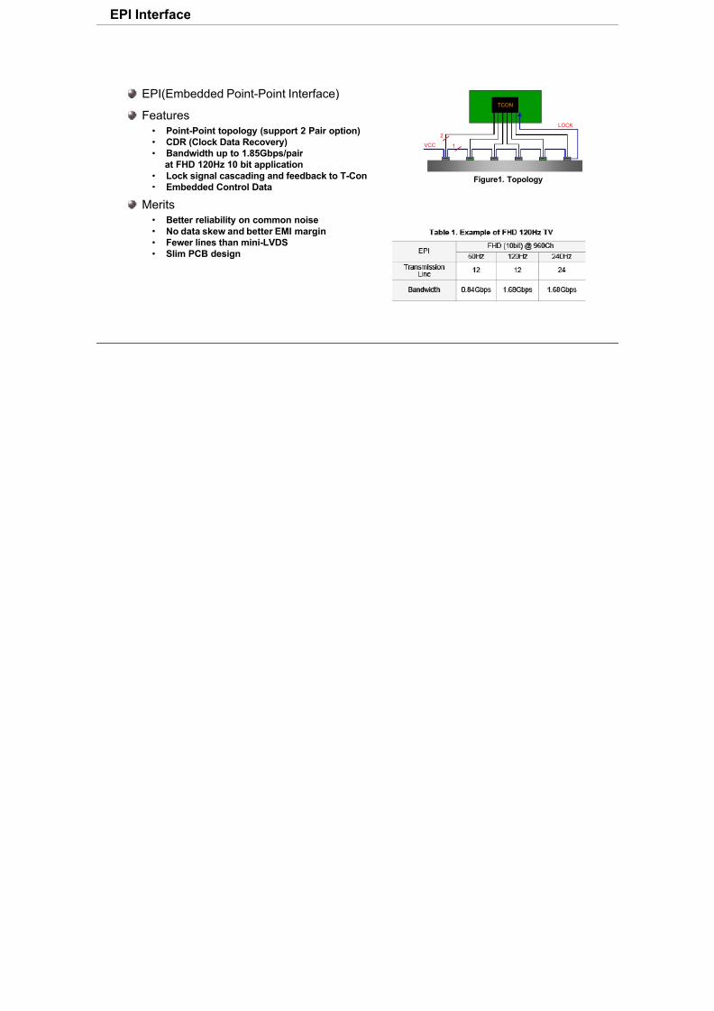
2013 LED/LCD TV
Engineering guide
< Applicable Model : High-end Platform >
EPI Interface
Page 55
7/21/2019 55LA860V, 860W, 868V, 8609
http://slidepdf.com/reader/full/55la860v-860w-868v-8609 55/127
EPI(Embedded Point-Point Interface)
Features
• Point-Point topology (support 2 Pair option)
• CDR (Clock Data Recovery)
• Bandwidth up to 1.85Gbps/pair
at FHD 120Hz 10 bit application
• Lock signal cascading and feedback to T-Con
• Embedded Control Data
Merits
• Better reliability on common noise
• No data skew and better EMI margin
• Fewer lines than mini-LVDS
• Slim PCB design
TCON
2
LOCK
VCC 1
Figure1. Topology
EPI Interface (mini-LVDS vs. EPI)
Page 56
7/21/2019 55LA860V, 860W, 868V, 8609
http://slidepdf.com/reader/full/55la860v-860w-868v-8609 56/127
Comparison
HF mini-LVDS
What to change
EPI (Embedded clock P-to-P Interface)
-Difficult to upgrade bandwidth limit
-Multiple number of wires needed for higher bandwidth
HF mini-LVDS
FHD (10bit)
60Hz 120Hz 240Hz
No. of Signal 36 36 72
Connector60pin(2ea)
60pin(2ea)
80pin(2ea)
-Better reliability on common noise
-No data skew. Better EMI margin-Lower cost ( Cable, Connector )
-Slim S-PCB design (14mm 10mm) helps slimmer TV
EPI
FHD (10bit)
60Hz 120Hz 240Hz
960ch 960ch 720ch
No. of Signal 12 12 32
Connector -50 pin(2ea)
70pin(2ea)
LCM (T-con to S-Driver IC)
TCON
2
LOCK
VCC 1
TCON
18
VCC 1
18
HF mini-LVDS
EPI
* Bandwidth Capability
- FHD 120Hz 10Bit : 594Mbps@36Lines → 1.65Gbps@12Lines
- FHD 240Hz 10Bit : 594Mbps@72Lines → 1.25Gbps@32Lines
(FHD 120Hz)
(FHD 120Hz)
HF mini-LVDS EPI
EPI Interface (mini-LVDS vs. EPI)
Page 57
7/21/2019 55LA860V, 860W, 868V, 8609
http://slidepdf.com/reader/full/55la860v-860w-868v-8609 57/127
Topology
Protocol
Features
@10bit, FHD120
• Multi Drop• Data rate: 660Mbps
• External clock
• Point to Point• Data rate : 1.8Gbps
• Embedded clock, Control
Merit• Simple structure
• Standardization
• Fewer Lines : 12
• Embedded clock
: low EMI, Clock skew free
• Easy to PCB design
Demerit
• Too many lines : 36
• Clock skew
• EMI due to clock lines
• Bandwidth limit
• Transmission Overhead
: 4bit delimiter
TCON
Lock
21
TCON
NFC (Near field communication)
Near field communication (NFC) is a set of standards for smartphones and similar devices to establish radio communication
with each other by touching them together or bringing them into close proximity, usually no more than a few centimetres.
Page 58
7/21/2019 55LA860V, 860W, 868V, 8609
http://slidepdf.com/reader/full/55la860v-860w-868v-8609 58/127
y g g g g p y, y
Present and anticipated applications include contactless transactions, data exchange, and simplified setup of more complex
communications such as Wi-Fi. Communication is also possible between an NFC device and an unpowered NFC chip, called
a "tag".
U
s
c
o
r
e
Samrt phone close to
NFC Tag
Player choose
From Smart phone
to TV
From TV
to Smart phone
Main PCB for Broadband Main + TCON all in one
xxLA790V-ZxChassis : LD34D
Page 59
7/21/2019 55LA860V, 860W, 868V, 8609
http://slidepdf.com/reader/full/55la860v-860w-868v-8609 59/127
To PSU
2
6
4
1Main processor, DDR Memory
eMMC Memory
2
3
4
Micom for Key/IR/Logo sensing
PMIC
Audio AMP
Key+IR+Logo
Front Spk
To module
5
5 EPI Wafer
Chassis : LD34D
PCB P/No : EAX65040103
3
6 Level shifter
WIFI/BT
1
Main PCB for Broadband Main + TCON all in one
xxLA860V-Zx Chassis : LD34DTo Camera
Page 60
7/21/2019 55LA860V, 860W, 868V, 8609
http://slidepdf.com/reader/full/55la860v-860w-868v-8609 60/127
To PSU
1Main processor, DDR Memory
eMMC Memory
2
3
4
Micom for Key/IR/Logo sensing
PMIC
Audio AMP
Key+IR+Logo
Front Spk
To module5 EPI Wafer
PCB P/No : EAX65040103
6 Level shifter
WIFI/BT
2
6
4
5
3
1
To Camera
7 USB 3.07
Main PCB for Broadband Main + TCON all in one
xxLA960V-Zx To LED Driver
Page 61
7/21/2019 55LA860V, 860W, 868V, 8609
http://slidepdf.com/reader/full/55la860v-860w-868v-8609 61/127
To PSU
1Main processor, DDR Memory
eMMC Memory
2
3
4
Micom for Key/IR/Logo sensing
USB 3.0
Audio AMP
Key+IR+Logo
Front Spk
To module5 LVDS Wafer
Chassis : LD34D
PCB P/No : EAX65040103
WIFI/BT
2
4
5
3
1
4
To CameraTo Woofer
1. H13 Block Diagram (External)
DAC_DATA
HSR P/M
PC_AUDIOPC_Audio_L/R
AV1 CVBSMotion-R
M-Remote_Rx/Tx
Page 62
7/21/2019 55LA860V, 860W, 868V, 8609
http://slidepdf.com/reader/full/55la860v-860w-868v-8609 62/127
16
DDR3
16
HSR_P/MAAD_DATA
CVBS
BB_TP_DATAAUD
Tuner
AV1_Audio L/RAV1
COMP1
AV1_CVBS
Comp1 Y,Pb,Pr
HDMI
SwitchHDMI2
HDMI3
H13
LG1154AN
USB1(USB3.0)
USB2(USB2.0)USB3(USB2.0)
AudioAMP
OPTIC
SPK
H/PLine out
H/P Audio L/R
SPDIF
I2S
DDR3
4Gb 2
(1600)
4Gb 2
(1600)
8
eMMC
4GB 1
SCART
SC_CVBS, RGB, Audio L/R
DTV/MNT_LR/V_OUT
LNB
HDMI_CEC
USB 3.0
USB 2.0
USB 2.0
USB 2.0
USB_W-iFi
PHYRMII
LAN
WOL / WOW
H/P AMP
H13
LG1154D
FRC
TCON
Logo Light
CI
CI
HDMI4
MHL1A
OCP1A
OCP1A
X-TAL
24MHZ
Woofer
HDMI1SPDIF_OUT_ARC
PMIC
LEVELSHIFTER
EPI
+3.3V_NOR
Ω
Ω +3.3V_TU
C7[SCL]
2. LG1154 I2C Map
Page 63
7/21/2019 55LA860V, 860W, 868V, 8609
http://slidepdf.com/reader/full/55la860v-860w-868v-8609 63/127
IC3201SII9587CNUC
HDMI_SW
IC7700TPS65178RSLR
EPI
AR15
[SCL0/GPIO66]
AP15[SDA0/GPIO65]
I2C_SDA1
IC5600
TAS5733AMP MAIN
24 [SCL]
23 [SDA]
IC5700
TAS5733
AMP WOOFER
33 Ω
33Ω
IC3000
R5F100GEAFB
RENESAS
MICOM
3 . 3 k Ω
I2C_SCL1
3 . 3 k Ω
+3.3V_NOR
3 . 3 k
3 . 3 k
AP6
[SCL3]
AR6[SDA3]
TU6503
TDSQ-G651D
TUNER_T2/C/S2
I2C_SDA4 35
I2C_SCL422 Ω
22 Ω
3 . 3 k Ω
3 . 3 k Ω
AR16
[SCL1/GPIO64]
AP16
[SDA1/GPIO79]
I2C_SDA_MICOM_SOC
I2C_SCL_MICOM_SOC1
2
H13
LG1154D
24 [SCL]
23 [SDA]
AR17
[SDA2/GPIO77]
AP17
[SCL2/GPIO78]
I2C_SDA2_SOC
I2C_SCL2_SOC
+3.3V_NOR
3 . 3 k Ω
3 . 3 k Ω
33 Ω
33 Ω
[P60/SCLA0]
[P61/SDAA0]
27
28
[SCL]
[SDA]
[D_SCL]
[D_SDA]
IC6900
A8303SESTR-T
LNB
7
8
33 Ω
33 Ω
[SCL]
[SDA]
AH32
[SCL4]
AJ33[SDA4]
I2C_SDA5
63
62
I2C_SCL5 33 Ω
33 Ω
3 . 3 k Ω
3 . 3 k Ω
+3.3V_NOR
[CSCL]
[CSDA]
IC102
R1EX24256BSAS0A
NVRAM
6
5
33 Ω
33 Ω
[SCL]
[SDA]
AH34[SCL5]
AH33[SDA5]
I2C_SDA6
3
4
I2C_SCL6 33 Ω
33 Ω
[SCL_T]
[SDA_T]
3 . 3 k Ω
3 . 3 k Ω
+3.3V_TU
33 Ω
33Ω
33 Ω
33Ω
IR Ass’y
MICOM
L Li ht A ’3 5V
3. Power Block Diagram
Page 64
7/21/2019 55LA860V, 860W, 868V, 8609
http://slidepdf.com/reader/full/55la860v-860w-868v-8609 64/127
1.0V Core
3A
1.8V_TU
5V Normal
5A
1.5V DDR
3A
Ethernet PHY
Wi-Fi Ass’y
Logo Light Ass’y
H13-D (VDDC)
DDR (VDDQ)
DDR (VDD)
3.5V
12V
24V
H13-A (VDDC10)
H13-A (AVDD10)
H13-A (XTAL)
1.2V Core
8A
H13-D (VDDC11)
H13-D (AVDD11)
H13-D (XTAL)
3.3V Normal
4A
1.23V_TU
2A
HDMI SW
SPDIF
Video Driver
AUDIO AMP
Headphone AMP
NVRAM
H13-D (VDD33)
H13-D (AVDD33)
H13-A (VDD33)
H13-A(AVDD33)
H13-A (VDD_XTAL)
EMMC(VCC)
EMMC(VCCQ)
TUNER(+3.3V_TU)
H13-D (VDD25)
H13-D (AVDD25)
H13-D (XTAL_VDDP)
H13-D (HDMI_VQPS)
H13-A (VDD25_CVBS)
H13-A (VDD25_AUD)
H13-A (VDD25_COMP)
H13-A (VDD25_VSB)
H13-A (VDD25_APLL)
H13-A(AVDD33)
H13-A (VDD_XTAL)
H13-A (SDRAM_VDDQ)
H13-A (AUAD_REF)
H13-A (VDD25_REF)
2.5V Normal
1.5A
AUDIO AMP
PANEL_VCC
LNB
SCART AMP
USB
HDMI SW
CI Slot
4. Tuner/CI Block Diagram
TDSQ-
G651D
+1 8 TU
+3.3V_TU
+3.3V_D_Demod
Page 65
7/21/2019 55LA860V, 860W, 868V, 8609
http://slidepdf.com/reader/full/55la860v-860w-868v-8609 65/127
LG1154
[RESET] 2 AG6[GPIO10]
AH34 [SCL5]
AH33 [SDA5]
[SLC] 3
[SDA] 4
[+3.3V_TUNER] 5
[+.1.8V_TUNER] 7
[CVBS] 8
[ERROR] 16[SYNC] 17
[VALID] 18
[MCLK] 19
AL37[TP_DVB_ERR]
AL36 [TP_DVB_SOP]AL35 [TP_DVB_VAL]
AM36 [TP_DVB_CLK]
[D0-7] 20-27
[+1.23V_S2_DEMOD] 30
[S2_RESET] 31 AM18 [ADIN7_SRV]
[+3.3V_S2_DEMOD] 32
LNB
IC6900A8303SESTR-TB
10 [TONECTRL]
2 [LNB]
7 [SCL]
8 [SDA]
[S2_F22_OUTPUT] 33
[LNB] 36
[S2_SCL] 34
[S2_SDA] 35
AP6 [SCL3]
AR6 [SDA3]
V15[CVBS_IN1]
H18[AAD_ADC_SIF]
/TU_RESET1
IC2_SCL6IC2_SDA6
FE_DEMOD1_TS_ERROR
FE_DEMOD1_TS_SYNC
FE_DEMOD1_TS_VAL
FE_DEMOD1_TS_CLK
FE_DEMOD1_TS_DATA [0-7]
+1.23V_D_Demod
/S2_RESET
LNB_TX
I2C_SCL4
I2C_SDA4
22 Ω
LNB_OUT
+3.3V_NORMAL
3.3K Ω
+1.8_TU
CVBS
TUNER_SIF
33 Ω 33Ω
33 Ω
CI Slot
100 Ω CI_TS_DATA[0-7]
/PCM_WE
/PCM_OE
/PCM_IRQA
/PCM_REG
PCM_INPACK
/PCM_WAIT
PCM_RST
CI_DATA[0-7] CI_A_DATA[0-7]
CI_ADDR[0-14] CI_A_ADDR[0-14]
/PCM_IORD
/PCM_IOWR
/PCM_CE2
/PCM_CE1
CI_VS1
/CI_CD1
/CI_CD2
CI 5V
Power detect
PCM_5V_CTL +5V_CI_ON
CI_TS_SYNC
CI_TS_VAL
CI_TS_CLK
[TP_DVB_DATA0-7]
TPO_DATA[0-7]
TPI_DATA[0-7]
CI_DET1D32[CAM_CD1_N]
CI_DET2E32[CAM_CD2_N]
VS1G32[CAM_VS1_N]
F33[CAM_CE1_N] CARD_EN1
CARD_EN2
10K Ω
H37[EB_BE_N0]
H36[EB_BE_N1]
IOWR
IORD
[EB_ADDR0-14]
[EB_DATA0-7]
ADDR[0-14]
DATA[0-7]
G34[CAM_RESET]
E33[CAM_WAIT]
D34[CAM_REG]
F32[CAM_IREQ]
J36[EB_OE]
H35[EB_WE]
A28[TPI_CLK]
B28[TPI_VAL]
B29[TPI_SOP]
TS_OUT_CLK
TS_OUT_VAL
TS_OUT_SYNC
CI_RESET
CI_WAIT
INPACK
REG
/IRQA
O_EN
WR_EN
VCC
H32
[CAM_VCCEN_N]
+5V_CI_ON +5V_NORMAL
10K Ω
CI_IN_TS_DATA[0-7]
100Ω
[SIF] 6
F34[CAM_CE2_N]
D33[CAM_INPACK]
5. Video & Audio IN
AV1
Jack Side SOC Side
Page 66
7/21/2019 55LA860V, 860W, 868V, 8609
http://slidepdf.com/reader/full/55la860v-860w-868v-8609 66/127
COMP1_PR_IN_SOC
COMP1_Y_IN_SOC
COMP1_PB_IN_SOC
COMP1_Y_IN_SOC_SOY
H13
(LG1154AN)
[CVBS_IN3]
AV1_CVBS_IN
AV1
Phone JACK
[AUAD_L/R_CH3_IN]
COMP1_Y/Pb/Pr
Component
1
Phone JACK
AV1_CVBS_IN_SOC
COMP2_PB_IN_SOC
COMP2_Y_IN_SOC
COMP2_Y_IN_SOC_SOY
COMP2_PR_IN_SOC
FULL
SCART
(18P)SC_CVBS_IN
[CVBS_IN2]
SC_CVBS_IN_SOC
SC_R
SC_G
SC_B
SC_CVBS_IN_SOY[PR1/Y1/PB1/SOY1_IN]
SC_L/R_IN AUAD_L/R_CH3_IN
[AUAD_L/R_CH2_IN]
COMP1/AV1/DVI_L_IN AUAD_L/R_CH2_IN
[PB2/Y2/SOY2/PR2_IN]
TunerTU_CVBS TU_CVBS_ISOC
[CVBS_IN1]TUNER_SIF_TU
DIF[P/N]
TUNER_SIF
ADC_I_INP/INN [AAD_ADC_SIF]
[ADC_I_INP/INN]
SC_FB
SC_IDSC_FB_SOC
SC_ID_SOC[SC1_SID]
[SC1_FB]
6. AUDIO OUT
T E SCART
MICOM
Page 67
7/21/2019 55LA860V, 860W, 868V, 8609
http://slidepdf.com/reader/full/55la860v-860w-868v-8609 67/127
SPDIF_OUT
TAS5733
AZ4580MTR
OP AMP
Mute
CTRL
[TR]
LPF
COMP1/AV1/DVI_L_IN
[IEC958OUT]
T u n e r
[AAD_ADC_SIF]
S C A R T_
M U T
AUDIO L/R OUT
I2C_SCL1/SDA1
MICOM
[AUD_SCART_OUTL/OUTR]
SC_L/R_IN
SCART_Lout/Rout
AUD_SCK/LRCK/LRCH
filter
AMP_MUTE
HP_L/ROUT_MAIN
SIDE_HP_MUTE
[DACSCK]
[DACLRCK]
[DACLRCH]
MAIN 4P wafer
[AUAD_L_CH2_IN]
[AUAD_L_CH3_IN]
[AUDA_OUTL]
H13
LG1154
[PHY0_ARC_OUT_0]
SPDIF_OUT_ARC
DTV/MNT_L/R_OUT
TUNER_SIF
[SCL0/SDA0]
LPF
TPA6138A2
Headphone
AMPLPF
HEADPHONE
LINE OUT
Phone Jack
LPF
AMP_RESET_N
HDMI1
HDMI_HPD_1 ~ 4 5V_HDMI_1 ~ 4
SPDIF_OUT_ARC
7. HDMI
Page 68
7/21/2019 55LA860V, 860W, 868V, 8609
http://slidepdf.com/reader/full/55la860v-860w-868v-8609 68/127
HDMI Switch
(IC3201 / SII9587CNUC)
HDMI Out put 8bits
I2C_SCL/SDA 5 2bits
CEC_REMOTE
MHL OCP
(IC3202 / TPS2554)
MHL_DET
SPDIF_OUT_ARC
HDMI_INT
HDMI_S/W_RESETHDMI_HPD_1
5V_HDMI_1
HDMI2
CEC_REMOTE
HDMI_HPD_2
5V_HDMI_2
HDMI3
CEC_REMOTE
HDMI_HPD_3
5V_HDMI_3
HDMI4
CEC_REMOTE
HDMI_HPD_4
5V_HDMI_4
H13D
(IC100 / LG1154D)
TMDS Link 8bits
TMDS Link 8bits
TMDS Link 8bits
TMDS Link 8bits
DDC_I2C 2bits
DDC_I2C 2bits
DDC_I2C 2bits
DDC_I2C 2bits
MICOM
(IC3000 / R5F100GEAFB)
CEC_REMOTE
(EPI CH1 ±)
(EPI CH3 ±)
TX0P/N
TX2P/N
(EPI CH2 ±)
TX1P/N
EPI 50P_LEFT
(LVDS_51PIN Side)
32/31
28/27
24/23
8. Panel Interface Block Diagram
Page 69
7/21/2019 55LA860V, 860W, 868V, 8609
http://slidepdf.com/reader/full/55la860v-860w-868v-8609 69/127
(EPI CH4 ±)
(EPI CH6 ±)
TX3P/N
TX5P/N
(EPI CH5 ±)TX4P/N
GMA_4/5/7/12/14/15
GMA _1 / 3 / 4 / 5 / 7 / 9 / 1 0 / 1 2 / 1
4 / 1 5 / 1 6 / 1 8
32/31
24/23
20/19
50~39
1~12
EPI_LOCK6_SOURCE
E P I _L O C K 3
15
14
36
CLK1/2/3/4/5/6 48~43
3~8
VGH_F/R
10/9
41/42
VGH_EVEN/ODD
12/11
39/40
VCOM_P/N
VCOM
17
34
VCOM_LOOP
VCOMLFB/RFB 16
35
GIP_RST
15
36
14
37VST
DISCHG
VGL
V GL _I
13
38
TX_LOCKN
Z _ O UT
1
50
VCC18
H_VDD
V core
VDD
VCC18
H_VDD
V core
VDD
VCC18
H_VDD
V core
VDD
H13
IC100
LG1154D
LEVEL SHIFTER
IC7701
TPS65198
CTRLN
VGL_FB
SWN
PMIC
IC7700
TPS65178RSLR
VCC
CTRLP
VGH_FB
SWP
VDD
VCOM_DYN
I2C_SDA2
PMIC_RESET
I2C_SCL2
GCLK
GST
MCLK
EO
GCLK
MCLK
EO
PANEL_VCC
VGL
VGH
PANEL_VCC
9. PMIC & Level Shift Bloc Diagram
Page 70
7/21/2019 55LA860V, 860W, 868V, 8609
http://slidepdf.com/reader/full/55la860v-860w-868v-8609 70/127
PMICTPS65178
Boost Converter
Buck 1 converter(VCC)
Buck 2 converter(Vcore)
Buck 3 converter(HVdd)
Buck 4 converter(VCC18)
Positive Charge Pump Controller
Negative Charge Pump Controller
6-Ch Gamma Buffer(DAC output)
Vcom reference & gain
Reset
VCC18
VCC
HVdd
Vdd
VCOM_P
VCOM_N
GAM4/5/7/12/14/15
CTRLN
SWP
SWN
CTRLP
VCOM_LOOP
PMIC_RESET
Vcore
Level ShiftTPS65198
TR/Diode
TR/
Diode
VGL
VGH
10. USB / WIFI / M-REMOTE / UARTUSB1(3.0)
USB3_DP
USB3_DM
[USB3_DP0]
[USB3_RX0M]
[USB3_RX0P]
[USB3_DM0] +5V_USB_1
USB3_RX0P
USB3_RX0M
Page 71
7/21/2019 55LA860V, 860W, 868V, 8609
http://slidepdf.com/reader/full/55la860v-860w-868v-8609 71/127
LG1154D_H13D
[ _ ]
[USB3_TX0M]
[USB3_TX0P]
USB2
USB_DP2
USB_DM2
[HUB_PORT_OVER0]
[HUB_VBUS_CTRL0]
OCP
OCP
+5V_USB_2
/USB_OCD1
USB_CTL1
USB_CTL2
/USB_OCD2
USB_WIFIWIFI_DM
WIFI_DP
Motion Remote
Receiver
M_REMOTE_RX
M_REMOTE_TX
M_RFModule_RESET
[UART1_RXD]
[UART1_TXD]
[UART1_RTS]
[UART1_CTS]
[USB2_0_DM]
[USB2_0_DP]
RENESAS MICOM
[UART0_RXD]
[UART0_TXD]
SOC_TX
SOC_RX
USB_DP3
+5V_USB_3
USB_CTL3
/USB_OCD3
[USB2_1_DM0]
[USB2_1_DP0]
[GPIO93][GPIO92]
[USB2_2_DM0][USB2_2_DP0]
USB3USB_DM3
[GPIO91][GPIO90]
M_REMOTE_CTS
M_REMOTE_RTS[GPIO13]
4Pin debugging
Wafer
USB3_TX0P
USB3+TX0M
Interconnection - 1
[PCBs]
47LA790V-ZA
Page 72
7/21/2019 55LA860V, 860W, 868V, 8609
http://slidepdf.com/reader/full/55la860v-860w-868v-8609 72/127
1 Main PCB
2 Power Board
3 Local key Assy
1
2
3
4
5
Main / LPB 24Pin + Local
Dimming Cable
Main / Module EPI Cable
50& 50Pin
LED driver / PSU
IR 8Pin Cable
WiFi 6Pin + RF 8Pin Cable
SPK Cable
[PCBs]
[Cables]
6
1
2
3
1
2
3
4
5
6
4 5
4 RF Assy
5 WIFI Assy
Interconnection - 2
47LA790V-ZA
Page 73
7/21/2019 55LA860V, 860W, 868V, 8609
http://slidepdf.com/reader/full/55la860v-860w-868v-8609 73/127
8
7 IR to Local Key 3Pin Cable
IR to Logo Assy 4Pin Cable
[Cables]
7
8
[PCBs]
6 IR Assy
6
Interconnection - 1
[PCBs]
55LA860V-ZA
Page 74
7/21/2019 55LA860V, 860W, 868V, 8609
http://slidepdf.com/reader/full/55la860v-860w-868v-8609 74/127
1 Main PCB
2 Power Board
3 Local key Assy
1
2
3
4
5
Main / LPB 24Pin + Local
Dimming Cable
Main / Module EPI Cable
50& 50Pin
LED driver / PSU
WiFi 6Pin + RF 8Pin Cable
SPK Cable
[PCBs]
[Cables]
1
2
3
1
2
3
4
5
45
4 RF Assy
5 WIFI Assy
6 Camera Assy
6
6 Camera Cable
6
Interconnection - 2
55LA860V-ZA
Page 75
7/21/2019 55LA860V, 860W, 868V, 8609
http://slidepdf.com/reader/full/55la860v-860w-868v-8609 75/127
8
7 IR to Local Key 3Pin Cable
IR cable
[Cables]
7
8
[PCBs]
7 IR Assy
7
Interconnection - 1
60LA860V-ZA
[PCBs]
Page 76
7/21/2019 55LA860V, 860W, 868V, 8609
http://slidepdf.com/reader/full/55la860v-860w-868v-8609 76/127
1
2
3
1
2
3
4
5
4 5
6
6
1 Main PCB
2 Power Board
3 Local key Assy
1
2
3
4
5
Main / PSU 18Pin
Main / T-con LVDS Cable
41& 51Pin
LED driver 14 Pin cable
WiFi 6Pin + RF 8Pin Cable
SPK Cable
[PCBs]
[Cables]
4 RF Assy
5 WIFI Assy
6 Camera Assy
7
6 Camera Cable
7 Local Dimming cable
Interconnection - 2
60LA860V-ZA
Page 77
7/21/2019 55LA860V, 860W, 868V, 8609
http://slidepdf.com/reader/full/55la860v-860w-868v-8609 77/127
9
8 IR to Local Key 3Pin Cable
IR 8 Pin Cable
[Cables]8
8
[PCBs]
6 IR Assy 7
7 LED Driver
8 T-con
6
8
Interconnection - 1
47LA960V-ZA
[PCBs]
Page 78
7/21/2019 55LA860V, 860W, 868V, 8609
http://slidepdf.com/reader/full/55la860v-860w-868v-8609 78/127
12
3
1
2
3
4
5
6
4 5
1 Main PCB
2 Power Board
3 Local key Assy
1
2
3
4
5
Main / PSU 18Pin
Main / T-con LVDS Cable
41& 51Pin
LED driver 14 Pin Cable
WiFi 6Pin + RF 8Pin Cable
SPK Cable
[ ]
[Cables]
4 RF Assy
5 WIFI Assy
6 Camera Assy
6 Camera Cable
7 Local Dimming cable
6
7
Interconnection - 2
47LA960V-ZA
Page 79
7/21/2019 55LA860V, 860W, 868V, 8609
http://slidepdf.com/reader/full/55la860v-860w-868v-8609 79/127
8
9
69
8 IR 5 Pin + Local Key 3 Pin Cable
Woofer Cable
[Cables]
[PCBs]
6 IR Assy
7 LED Driver
8 T-con
7
8
f
Page 80
7/21/2019 55LA860V, 860W, 868V, 8609
http://slidepdf.com/reader/full/55la860v-860w-868v-8609 80/127
Introductions of 13Y RF ass’y + Magic Remote control
1. System
2. Remote Buttons
3. MR13 Block Diagram
4. Function List
5. Pairing/Un-pairing Method
1. System
UART
or USBRF
Page 81
7/21/2019 55LA860V, 860W, 868V, 8609
http://slidepdf.com/reader/full/55la860v-860w-868v-8609 81/127
Remote
RF Receiver
TV
Pairing Information Transm ission (Send to TV after Paired)
• Static Calibration Data (Bypass only)
• Remote FW ver. (Save also in Receiver)
• BD_ADDR (Save also in Receiver)
• Pairing Information Transm ission Sequence
• When it is paired, the remote sends packets(pairing success, F/W version, BD_ADDR) to the receiver.• The receiver sends the pairing success packet to TV directly.
• F/W version and BD_ADDR packets are just saved on the receiver.
• The receiver sends F/W version or BD_ADDR packet to TV when it is required.
Motion Data Transmiss ion
• Period : 7.5msec
• Motion Data : gyro, accelerometer
Voice Data Transmissio n
• Period : 10msec• Voice sampling : 16khz 16bit
2. Remote Buttons (M4 vs. MR13P)
BUTTONRF Unpaired
IR_CODE
RF Paired
RF_CODE
IR continuous
repeatETC.
POWER 0x08 NONE Y IR only
POWER
Page 82
7/21/2019 55LA860V, 860W, 868V, 8609
http://slidepdf.com/reader/full/55la860v-860w-868v-8609 82/127
Phsical
Buttons
y
BACK 0x28 0x8028 Y
SMART 0x7C 0x807C Y
← 0x07 0x8007 Y
→ 0x06 0x8006 Y
↑ 0x40 0x8040 Y
↓ 0x41 0x8041 Y
OK 0x75 0x8044 Y
VOICE 0xDE 0x808B Y = VOICE_START
3D 0xDC 0x80DC Y
Screen RMT
/ Q.MENU0xDE 0x80DE Y
CH + 0x00 0x8000 Y
CH - 0x01 0x8001 Y
VOL + 0x02 0x8002 Y
VOL - 0x03 0x8003 Y
MUTE 0x09 0x8009 Y
Logical
Buttons
AUTO_WAKEUP X 0x800C
VOICE_START X 0x800A
VOICE_STOP X 0x800D
POINT_START X 0x803E
POINT_STOP X 0x803FM4 Remote MR13P Remote
POWER
BACK HOME
↑
OK← →
↓
MUTEVOL CH
3D MYAPPS
↑
OK← →
↓
VOICEBACK SMART
3D
Screen RMT
Q.MENU
MUTEVOL CH
LED
3. MR13P Block Diagram
MPU-6150
(Gyro+ACC)I2C ch1 IR Emitter1
Antenna
Page 83
7/21/2019 55LA860V, 860W, 868V, 8609
http://slidepdf.com/reader/full/55la860v-860w-868v-8609 83/127
(Gyro+ACC)
(Invensense)
BCM20733M A2 (BROADCOM)
Bluetooth 3.0Key Button
( 4 x 4 )
AA x 2 Battery DC-DC Boost
TI TPS61097
SOT23-5
Power Management
Antenna
Partron
X-tal
24 MHz
2.8V LDOuP0108NEC5-28
SC70
512Kb
(Serial F/M)
I2C ch2
WM8950
(Wolfson)
Voice
MIC.
(Knowles)
I2S
4-mode Only
2.8V LDOuP0108NEC5-28
SC70
Wheel
Encoder
IR Emitter2
(Voice Scene IR)
Codec(ADC )
Bluetooth Receiver
BCM20702M(BROADCOM)
Bluetooth 4.0
Antenna
Connector
X-tal
20 MHz
512Kbit
(Serial Flash)
UART
SPI
Bluetooth Remote control
Light
Control
주요
Item IC Manufacturer Function
4. Function list
Page 84
7/21/2019 55LA860V, 860W, 868V, 8609
http://slidepdf.com/reader/full/55la860v-860w-868v-8609 84/127
Remocon
Voice
Voice Codec WM8950 Wolfson 16KHz Sampling of Audio data
MEMS Mic. SPU0414HR5H Knowles Sensing Voice
Motion
Sensor
Gyro Sensor
+
Accelerometer
MPU-6150 Invensense
Sensing angular velocity of X, Y, Z-axis
Sensing device tilt (Pitch & Roll angle)
RF
+
Micom
RF Antenna SDBTPTR3015 Partron
Wireless communicationX-tal 24MHz Partron
RF + Micom BCM20733A2 Broadcom
DC-DC Converter TPS61097 TI Battery Boost up Regulator
LDO1 uP0108NEC5-28 uPI RF, Gyro, Accelerometer Power Supply
LDO2 uP0108NEC5-28 uPI Audio Codec, Mic. Power Supply
5. RF Pairing / Un-pairing Method
Method Description
• When do pairing, the remote
Page 85
7/21/2019 55LA860V, 860W, 868V, 8609
http://slidepdf.com/reader/full/55la860v-860w-868v-8609 85/127
RF Pairing
Method1
– If unpaired, just press "OK" button.
– If paired, press "OK" button after
unpairing.
Method 2 (Repairing)
– Press “BACK" button for 5 sec.
should make pairing request IR
signal(0x75) to TV.
• When TV receive the IR signal, it
should send "pairing request
packet" to the RF receiver.
• After pairing success, the remote
should blink LED for some time and
TV send "pairing success packet"
back to TV.
• When remote try to unpairing, it
doesn’t care about state ofreceiver(stand alone).
RF UnpairingPress “BACK" button and “SMART" button
at the same time for 5 sec.
• When remote try to unpairing, it
doesn’t care about state of
receiver(stand alone).
• After unpairing, all pairing
information should be erased.
• After unpairing, LED should be
blinked for 3sec.
• The remote just becomes to IR
mode.
Introductions of 13Y WIFI built in ass’y
Page 86
7/21/2019 55LA860V, 860W, 868V, 8609
http://slidepdf.com/reader/full/55la860v-860w-868v-8609 86/127
1. Wi-Fi built in Ass’y feature
2. Wi-Fi built in Ass’y
specification
Introductions of 13Y WIFI built in ass y
WIFI Built in ass’y featureBlock diagram
Page 87
7/21/2019 55LA860V, 860W, 868V, 8609
http://slidepdf.com/reader/full/55la860v-860w-868v-8609 87/127
PIN
US interface
1 Vcc
2 DM
3 DP
4
GND5 WOW
6 NC
- Pin map
BCM43236B
Wafer
6pin 1.25mm
3.3V
USB
DP, DN
GND
USB
DP, DN
DCDC
EUP3010
Crystal
20MHz
3.3V 1.2V
3.3V 1.2V
Switch
DM3030Antenna
2.4G/5G
Antenna
2.4G/5G
RX/TX
RX/TX
WOL
Switch
DM3030
48
30
WIFI Built in ass’y Specification
Page 88
7/21/2019 55LA860V, 860W, 868V, 8609
http://slidepdf.com/reader/full/55la860v-860w-868v-8609 88/127
Contents of LCD TV Standard Repair Process
No. Error symptom (High category) Error symptom (Mid category) Page Remarks
1 No video/Normal audio 1
Page 89
7/21/2019 55LA860V, 860W, 868V, 8609
http://slidepdf.com/reader/full/55la860v-860w-868v-8609 89/127
A. Video error
2 No video/No audio 2
3 Video error, video lag/stop, fail tunning 3, 4
4 Color error 5
5Vertical/Horizontal bar, residual image, light
spot, external device color error6
6
B. Power error
No power 7
7Off when on, off while viewing, power autoon/off
8
8 C. Audio error No audio/Normal video 9
9 Wrecked audio/discontinuation/noise 10
10D. Function error
No response in remote controller, key error,recording error, memory error
11
11 External device recognition error 12
12 E. Noise Circuit noise, mechanical noise 13
13 F. Exterior error Exterior defect 14
14 G. Network error Connection defect / Network speed low 15
First of all, Check whether there is SVC Bulletin in GCSC System for these model.
Contents of LCD TV Standard Repair Process Detail Technical ManualNo. Error symptom Content Page Remarks
1
A. Video error_ No video/Normal audio
Check LCD back light with naked eye A1
2 LED driver B+ 24V measuring method A2
3 Ch k Whit B l l A3
Page 90
7/21/2019 55LA860V, 860W, 868V, 8609
http://slidepdf.com/reader/full/55la860v-860w-868v-8609 90/127
3 Check White Balance value A3
4 Power Board voltage measuring method A4
6 A. Video error_ No video/Video lag/stop TUNER input signal strength checking method A67 LCD-TV Version checking method A7
9
A. Video error_Color error
LCD TV connection diagram A8
10 Tuner Checking Part A9
11Check Link Cable (LVDS) reconnectioncondition
A10
A11
A10 : 32/37/42/47/55
A11 : 32 AUO
12 Adjustment Test pattern - ADJ Key A12
13
A. Video error_Vertical/Horizontal bar,residual image, light spot
LCD TV connection diagram A8
14Check Link Cable (LVDS) reconnectioncondition
A10
A11
A10 : 32/37/42/47/55
A11 : 32 AUO
15 Adjustment Test pattern - ADJ Key A12
16
<Appendix>
Defected Type caused by T-Con/Inverter/ Module
Exchange T-Con Board (1) A-1/5
17 Exchange T-Con Board (2) A-2/5
18 Exchange LED driver Board (PSU) A-3/5
55” : driver board
Other : PSU
19 Exchange Module itself (1) A-4/5
20 Exchange Module itself (2) A-5/5
Continue to the next page
Established
date
Standard Repair Process
Revised dateLCD TV
Error
symptom
A. Video error
No video/ Normal audio
Fi t f ll Ch k h th ll f bl b t b d i i t d l t
2012. 12 .06
Page 91
7/21/2019 55LA860V, 860W, 868V, 8609
http://slidepdf.com/reader/full/55la860v-860w-868v-8609 91/127
Normal
audio
Y
N
Move to No
video/No audio
No video
Normal audioCheck Back Light
On with naked eyeOn
Y
N
Check Power Board12v,3.5v etc.
Normal
voltage
Y
N
Replace T-con Board
or module
And Adjust VCOM
Repair Power Board
or partsCheck Power Board 24v output
Normal
voltage
YReplace Inverter
or module
N
Repair Power
Board or parts
End
Always check & record S/W Version and WhiteBalance value before replacing the Main Board
Replace Main Board Re-enter White Balance value
※Precaution
☞
A4A1
☞A2
☞A28
☞
A7 & A3
First of all, Check whether all of cables between board is inserted properly or not.(Main B/D↔ Power B/D, LVDS Cable,Speaker Cable,IR B/D Cable,,,)
Standard Repair Process
A. Video error
No video/ No audio
Established
date
Revised dateLCD TV
Error
symptom
2012. 12 .06
Page 92
7/21/2019 55LA860V, 860W, 868V, 8609
http://slidepdf.com/reader/full/55la860v-860w-868v-8609 92/127
Normal
voltage?
Check various voltages
of Power Board
( 3.5V,12V,20V or 24V…) No Video/
No audio
Check and
replace
MAIN B/D
Y
Replace Power
Board and repair
parts
N End
☞A4
A. Picture Problem
Picture broken/ Freezing
Standard Repair Process
Established
date
Revised dateLCD TV
Error
symptom
2012. 12 .06
Page 93
7/21/2019 55LA860V, 860W, 868V, 8609
http://slidepdf.com/reader/full/55la860v-860w-868v-8609 93/127
Y
N
☞ A6
N
Check RF Signal level
Normal
Signal?
Check RF Cable
Connection
1. Reconnection
2. Install Booster
CheckS/W Version
Use Signal TestCheck Signal status
S/W Upgrade
Check whether other equipments have problem or not.
(By connecting RF Cable at other equipment)
→ DVD Player ,Set-Top-Box, Different maker TV etc`
SVCBulletin?
Replace
Main B/D
Check
Tuner soldering
Normal
Picture?
Y
N
Y
Close
NormalPicture?
Y Close
. By using Digital signal level meter
. By using Diagnostics menu on OSD( Menu→ Set up→ Support → Signal Test )
- Signal strength (Normal : over 50%)- Signal Quality (Normal: over 50%)
NormalPicture?
Y
Contact with signal distributor
or broadcaster (Cable or Air)
NN
Normal
Picture?
Y
Close
N
☞
A7
A. Picture Problem (DVB-S/S2)
Tuning fail, Picture broken/ Freezing
Standard Repair Process
Established
date
Revised dateLCD TV
Error
symptom
2012. 12 .06
Page 94
7/21/2019 55LA860V, 860W, 868V, 8609
http://slidepdf.com/reader/full/55la860v-860w-868v-8609 94/127
Y N
☞ A6
Check RF Signal level
Normal
Signal?
Check
S/W Version
S/W Upgrade
SVC
Bulletin?
Normal
Picture?
Y
N
Y
Close
Check RF signal cable (DVB satellite signal or not)
Check whether other equipments have problem or not.(By connecting RF Cable at other equipment)
→ Set-Top-Box, Different maker TV etc
Y
Change satellite setting
(match with installed ANT)
N
Normal
Picture?
Y
Close
N
☞
A7Check satellite setting.
- Check LNB frequency.
- Check satellite
- Check Satellite connection
(DiSEqC, motor, etc…)
Normal
setting?
Contact with
signal distributor
or broadcaster
(Cable or Air)
Close
N
Check
Tuner soldering
Replace
Main B/D
A. Video error
Color error
Standard Repair Process
Established
date
Revised dateLCD TV
Error
symptom
2012. 12 .06
Page 95
7/21/2019 55LA860V, 860W, 868V, 8609
http://slidepdf.com/reader/full/55la860v-860w-868v-8609 95/127
Color
error?
Y
N
※
Check andreplace Link
Cable
(LVDS) and
contact
condition
Y
N
Replace Main B/DColor
error?
Check error color
input mode
Check color by input
-External Input
-COMPONENT
-RGB
-HDMI/DVI
YExternal device
/Cable
normal
External Input/
Component
error
Checkexternal
device and
cable
YExternal device
/Cablenormal
RGB/
HDMI/DVIerror
Check external
device andcable
Replace Main B/D
Replace Main B/D
N
N
☞
A8
N
Y
End
Replace module
Request repair
for external
device/cable
Color
error?
Check Test pattern☞
A12
☞
A10/ A11
Vertical/Horizontal bar, residual image, light spot
A. Video error
Vertical / Horizontal bar, residual image,light spot, external device color error
Replace
Established
date
Revised dateLCD TV
Error
symptom
Standard Repair Process
2012. 12 .06
Page 96
7/21/2019 55LA860V, 860W, 868V, 8609
http://slidepdf.com/reader/full/55la860v-860w-868v-8609 96/127
Screen
normal?
N
Y Check externaldevice
connection
condition
Y
N
Check andreplace Link
CableNormal?
Y
NScreen
normal?
Replace Main B/D
(adjust VCOM)
Replace
module
Check color condition by input
-External Input
-Component
-RGB
-HDMI/DVI
End
, g , g p
Request repair
for external
device☞A12
External device screen error-Color errorExternal
Input
error
Connect other external
device and cable(Check normal operation of
External Input, Component,
RGB and HDMI/DVI by
connecting Jig, pattern
Generator ,Set-top Box etc.
N
Y
Replace
Main B/D
Screen
normal?
Check screen
condition by input
-External Input-Component
-RGB
-HDMI/DVI
Request repair forexternal device
Component
error
RGB
error
HDMI/
DVI
Connect other external
device and cable(Check normal operation of
External Input, Component,
RGB and HDMI/DVI by
connecting Jig, pattern
Generator ,Set-top Box etc.
Replace
Main B/DScreen
normal?
N
Y
Check S/W Version
Y
NCheck
version
S/W Upgrade
Y
N
Normal
screen?
End
Y
N
Replace Main B/D
For LGD panel
Module
Screen
normal?
End
☞
A8☞
A10/ A11
Check Test pattern
☞
A28
For other panel
B. Power error
No power
Standard Repair Process
Established
date
Revised dateLCD TV
Error
symptom
2012. 12 .06
Page 97
7/21/2019 55LA860V, 860W, 868V, 8609
http://slidepdf.com/reader/full/55la860v-860w-868v-8609 97/127
Power LEDOn?
Y
N
DC Power on
by pressing Power KeyOn Remote control
Y
NNormaloperation? Check Power
On ‘”High”
Check Power cord
was inserted properly
CheckPower LED
Replace
Power
B/D
Measure voltage of each output of Power B/D
N
YNormal
voltage?Replace Main B/D
YOK?
Replace Main B/D
N
Y
Normal?
Check ST-BY 3.5V
Replace Power B/D
N
YNormal
voltage?
Replace Power
B/D
Y
☞
A17
☞
A18
☞
A19
☞
A4
. Stand-By: Red
. Operating: white
Close
B. Power error
Off when on, off while viewing, power auto on/off
Check outletA22
Established
date
Revised dateLCD TV
Error
symptom
Standard Repair Process
2012. 12 .06
Page 98
7/21/2019 55LA860V, 860W, 868V, 8609
http://slidepdf.com/reader/full/55la860v-860w-868v-8609 98/127
Error?N
Y
Check Power Off
Mode
Fix A/C cord & Outlet
and check each 3
phase out
Check A/C cord
Check for all 3- phase
power out
Replace Main B/DCPU
Abnormal
(If Power Off mode is
not displayed)
Check Power B/D
voltage
Y
N
Replace Main B/DNormal
voltage?
Replace Power B/D
Replace Power B/D
N
YNormal? End
※ CautionCheck and fix exterior
of Power B/D Part
☞A22
☞
A19
Status Power off List Explanation
Normal
"POWEROFF_REMOTEKEY" Power off by REMOTE CONTROL
"POWEROFF_OFFTIMER" Power off by OFF TIMER
"POWEROFF_SLEEPTIMER" Power off by SLEEP TIMER
"POWEROFF_INSTOP" Power off by INSTOP KEY
"POWEROFF_AUTOOFF" Power off by AUTO OFF
"POWEROFF_ONTIMER" Power off by ON TIMER
"POWEROFF_RS232C" Power off by RS232C
"POWEROFF_RESREC" Power off by Reservated Record
"POWEROFF_RECEND" Power off by End of Recording
"POWEROFF_SWDOWN" Power off by S/W Download
"POWEROFF_UNKNOWN" Power off by unknown status except listed case
Abnormal
POWEROFF_ABNORMAL1 Power off by abnormal status except CPU trouble
POWEROFF_CPUABNORMAL Power off by CPU Abnormal
* Please refer to the all cases which
can be displayed on power off mode.
Abnormal
1
C. Audio error
No audio/ Normal video
Established
date
Revised dateLCD TV
Error
symptom
Standard Repair Process
2012. 12 .06
Page 99
7/21/2019 55LA860V, 860W, 868V, 8609
http://slidepdf.com/reader/full/55la860v-860w-868v-8609 99/127
No audio
Screen normal
Check user
menu >
Speaker offOff
N
Y
Cancel OFF
Check audio B+ 24V
of Power BoardNormal
voltage
Y
N
Replace Power Board and repair parts
Check Speaker
disconnection
N
Y
Replace Speaker
Replace MAIN Board End
☞
A24☞
A25
Disconnection
→ abnormal audio/discontinuation/noise is same after “Check input signal” compared to No audio
C. Audio error
Wrecked audio/ discontinuation/noise
Established
date
Revised dateLCD TV
Error
symptom
Standard Repair Process
2012. 12 .06
Page 100
7/21/2019 55LA860V, 860W, 868V, 8609
http://slidepdf.com/reader/full/55la860v-860w-868v-8609 100/127
Wrecked audio/
Discontinuation/
Noise for
all audio
Check and replacespeaker and
connector
Wrecked audio/
Discontinuation/
Noise only
for D-TV
Wrecked audio/
Discontinuation/
Noise onlyfor Analog
Wrecked audio/
Discontinuation/
Noise only
for External Input
Connect and checkother external device
N
Y
Normal
audio?
Check and fix external device
Replace Power B/D
N
Y
Normal
voltage?
Check input
signal
-RF
-External Input
signal
Signal
normal?
(When RF signal is not
received)
Request repair to external
cable/ANT provider
Y
Check audio
B+ Voltage (24V)
Replace Main B/D
(In case of External
Input signal error)
Check and fix
external device
Replace Main B/DN
End
☞A25
D. General Function Problem
Remote control & Local switch checking
1. Remote control(R/C) operating error Replace
Standard Repair Process
Established
date
Revised dateLCD TV
Error
symptom
2012. 12 .06
Page 101
7/21/2019 55LA860V, 860W, 868V, 8609
http://slidepdf.com/reader/full/55la860v-860w-868v-8609 101/127
Y
N
( ) p g
Check R/C itselfOperation
Normaloperating?
Normaloperating?
Y
Close
Replace R/C
If R/C operate,
Explain the customer
cause is interferencefrom light in room.
Check R/C Operating
When turn off light
in room
Check & Replace
Baterry of R/C
Check & RepairCable connection
Connector solder
Normaloperating?
Check B+ 3.5VOn Main B/D
☞A27
NormalVoltage?
Close
N
N
Check 3.5v on Power B/D
Replace Power B/D or
Replace Main B/D
(Power B/D don’t have problem)
☞
A4
Check IROutput signal
NormalSignal?
N
Y
Repair/Replace
IR B/D
N
☞
A27
p
Main B/D
Y
☞A27
D. Function error
External device recognition error
Established
date
Revised dateLCD TV
Error
symptom
Standard Repair Process
2012. 12 .06
Page 102
7/21/2019 55LA860V, 860W, 868V, 8609
http://slidepdf.com/reader/full/55la860v-860w-868v-8609 102/127
Check technical
information
- Fix information
- S/W Version
N
Y
Technical
information?
Check
input
signal
Signal
input?
Y
N
External Input and
Component
Recognition error
Check and fix
external device/cable
RGB,HDMI/
DVI, Optical
Recognition error
Replace Main B/D
Replace Main B/DFix in
accordance
with technical
information
E. Noise
Circuit noise, mechanical noise
Established
date
Revised dateLCD TV
Error
symptom
Standard Repair Process
2012. 12 .06
Page 103
7/21/2019 55LA860V, 860W, 868V, 8609
http://slidepdf.com/reader/full/55la860v-860w-868v-8609 103/127
Check location
of noiseIdentify
noise type
Circuit
noise
Replace PSU(with LED driver)
Replace LED driver
Mechanical
noise
Check location of
noise
OR
※ When the nose is severe, replace the module
(For models with fix information, upgrade the S/W or
provide the description)
※ If there is a “Tak Tak” noise from the cabinet,refer to the KMS fix information and then proceed
as shown in the solution manual
(For models without any fix information, provide
the description)
OR
※ Mechanical noise is a natural
phenomenon, and apply the 1st level
description. When the customer does not
agree, apply the process by stage.
※ Describe the basis of the description in
“Part related to nose” in the Owner’s Manual.
F. Exterior defect
Exterior defect
Established
date
Revised dateLCD TV
Error
symptom
Standard Repair Process
2012. 12 .06
Page 104
7/21/2019 55LA860V, 860W, 868V, 8609
http://slidepdf.com/reader/full/55la860v-860w-868v-8609 104/127
Replace moduleZoom part with
exterior damageModule
damage
Cabinet
damageReplace cabinet
Replace remote controller
Remote
controller
damage
Stand
dentReplace stand
Adjust VCOM
☞
A28
G. Network Error
Exterior defect
Established
date
Revised dateLCD TV
Error
symptom
Standard Repair Process
2012. 12 .06
Check Wired ethernet cable connection
Page 105
7/21/2019 55LA860V, 860W, 868V, 8609
http://slidepdf.com/reader/full/55la860v-860w-868v-8609 105/127
Y N
Check Network status
Normal
Signal?
Check
S/W Version
S/W Upgrade
SVC
Bulletin?
Normal
Picture?
Y
N
Y
Close
Check Wired ethernet cable connection
Check whether AP has a probelm or not.
Setting Network Networ Status
Y
Try to new network connection
(match with AP and ether setting)
N
Normal
Picture?
Y
Close
N
☞
A7Check Network connection
Case1 WiFi .
- Check AP status
Case2 Wired
- Check ethernet Port
Normal
setting?
Check connection
with AP or internet
(WiFi = AP)
(Wired = ethernet
port)
Close
N
Check
Wired, Wifi status
(Cable / sub Assy)
Replace
Main B/D
G. CI+ Competibility Error
Exterior defect
Established
date
Revised dateLCD TV
Error
symptom
Standard Repair Process
2012. 12 .06
Check defect CI slot pin
Page 106
7/21/2019 55LA860V, 860W, 868V, 8609
http://slidepdf.com/reader/full/55la860v-860w-868v-8609 106/127
Y N
Check CI CAM status
Read
Information?
Check
CAM S/W
Version
CAM S/W Upgrade
By OTA
SVC
Bulletin?
Normal
Picture?
Y
N
Y
Close
p
Check it’s worked CI+ 1.2 or 1.3
Setting Antenna CI information
Y
N
Check status of CI+ Key in the
In-start menuIs there
CI+ key?
Check damage of CI slot pin
Or damage of CI CAM
Close
N
Check
Wired, Wifi status
(Cable / sub Assy)
Replace
Main B/D
Replace
Main B/D
Or
Download
CI+ Key
Old version of CI+ 1.2 CAM is not worked at the TV that is supported CI+ 1.3
Check SVC Bulletin
Contents of LCD TV Standard Repair Process Detail Technical Manual
No. Error symptom Content Page Remarks
21 Check front display LED A17
22 Check power input Voltage & ST-BY 3.5V A18
Continued from previous page
Page 107
7/21/2019 55LA860V, 860W, 868V, 8609
http://slidepdf.com/reader/full/55la860v-860w-868v-8609 107/127
B. Power error_No power23 Checking method when power is ON A19
24 POWER BOARD voltage measuring method A5
25
26B. Power error_Off when on, off whileviewing
POWER OFF MODE checking method A22
27B. Power error_Off when on, off whileviewing
POWER BOARD PIN voltage checking method A19
28
C. Audio error_No audio/Normal video
Checking method in menu when there is noaudio
A24
29Voltage and speaker checking method whenthere is no audio
A25
30C. Audio error_Wreckedaudio/discontinuation
Voltage and speaker checking method incase of audio error
A25
31D. Function error_ No response inremote controller, key error
Remote controller operation checking method A27
32 D. VCOM Adjustment Sequence of the Vcom adjustment A28
Standard Repair Process Detail Technical Manual
Check White Balance value
A. Video error_No video/Normal audio
<ALL MODELS>
A4
Establisheddate
Reviseddate
Error
symptom
Content
LCD TV2012. 12 .06
Page 108
7/21/2019 55LA860V, 860W, 868V, 8609
http://slidepdf.com/reader/full/55la860v-860w-868v-8609 108/127
Entry method
1. Press the ADJ button on the remote controller for adjustment.
2. Enter into White Balance of item 10.
3. After recording the R, G, B (GAIN, Cut) value of Color Temp (Cool/Medium/Warm), re-
enter the value after replacing the MAIN BOARD.
Standard Repair Process Detail Technical Manual
Power Board voltage measuring method
A. Video error_No video/ Audio
A5
Establisheddate
Reviseddate
Error
symptom
Content
LCD TV
Check the DC 24V 12V 3 5V
2012. 12 .06
Page 109
7/21/2019 55LA860V, 860W, 868V, 8609
http://slidepdf.com/reader/full/55la860v-860w-868v-8609 109/127
Check the DC 24V, 12V, 3.5V.
24 Pin
Power Board ↔ Main Board)
SMAW200-H24S
1 Power on 2 Inverter On/off
3
3.5V
4
PWM Dim #1
5
3.5V
6
PWM Dim #2
7 GND 8 GND
9
24V
10
24V
11 GND 12 GND
13 12V 14 12V
15 12V 16
24V
17 GND 18 GND
19 GND 20 GND
21 GND 22
L/DIMO_VS
23 L/DIM0_MOSI 24 L/DIM0_SCLK
Standard Repair Process Detail Technical Manual
TUNER input signal strength checking method
A. Video error_Video error, video lag/stop
<ALL MODELS>
A6
Establisheddate
Reviseddate
Error
symptom
Content
LCD TV2012. 12 .06
Page 110
7/21/2019 55LA860V, 860W, 868V, 8609
http://slidepdf.com/reader/full/55la860v-860w-868v-8609 110/127
MENU support signal test
select channel
When the signal is strong, use the
attenuator (-10dB, -15dB, -20dB etc.)
Standard Repair Process Detail Technical Manual
LCD-TV Version checking method
A. Video error_Video error, video lag/stop
1. Checking method for remote controller for adjustment<ALL MODELS>
A7
Establisheddate
Reviseddate
Error
symptom
Content
LCD TV2012. 12 .06
Page 111
7/21/2019 55LA860V, 860W, 868V, 8609
http://slidepdf.com/reader/full/55la860v-860w-868v-8609 111/127
Press the IN-START with the remote
controller for adjustment
Version
Standard Repair Process Detail Technical Manual
LCD TV connection diagram (1)
A. Video error _Vertical/Horizontal bar, residualimage, light spot
A8
Establisheddate
Reviseddate
Error
symptom
Content
LCD TV
<ALL MODELS>
2012. 12 .06
Page 112
7/21/2019 55LA860V, 860W, 868V, 8609
http://slidepdf.com/reader/full/55la860v-860w-868v-8609 112/127
As the part connecting to the external input, check the screen condition by signal
Standard Repair Process Detail Technical Manual
TUNER checking part
A. Video error_Video error, video lag/stop
<ALL MODELS>
A9
Establisheddate
Reviseddate
Error
symptom
Content
LCD TV2012. 12 .06
Page 113
7/21/2019 55LA860V, 860W, 868V, 8609
http://slidepdf.com/reader/full/55la860v-860w-868v-8609 113/127
Checking method:
1. Check the signal strength or check whether the screen is normal when the external device is connected.
2. After measuring each voltage from power supply, finally replace the MAIN BOARD.
Standard Repair Process Detail Technical Manual
Adjustment Test pattern - ADJ Key
A. Video error_Color error
A12
EstablisheddateRevised
date
Error
symptom
Content
LCD TV 2012. 12 .06
Page 114
7/21/2019 55LA860V, 860W, 868V, 8609
http://slidepdf.com/reader/full/55la860v-860w-868v-8609 114/127
You can view 6 types of patterns using the ADJ Key
Checking item : 1. Defective pixel 2. Residual image 3. MODULE error (ADD-BAR,SCAN BAR..)
4.Video error (Classification of MODULE or Main-B/D!)
Appendix : Exchange EPI Cable or Main B/D (1)
Page 115
7/21/2019 55LA860V, 860W, 868V, 8609
http://slidepdf.com/reader/full/55la860v-860w-868v-8609 115/127
Solder defect, CNT Broken
T-Con Defect, CNT BrokenT-Con Defect, CNT BrokenT-Con Defect, CNT Broken
Solder defect, CNT Broken Solder defect, CNT Broken
Solder defect, CNT Broken Solder defect, CNT Broken Abnormal Power Section
Solder defect, Short/Crack Abnormal Power Section Solder defect, Short/Crack
Appendix : Exchange EPI Cable or Main B/D (2)
Page 116
7/21/2019 55LA860V, 860W, 868V, 8609
http://slidepdf.com/reader/full/55la860v-860w-868v-8609 116/127
Abnormal Power Section Solder defect, Short/Crack Abnormal Power Section
Solder defect, Short/Crack Fuse Open, Abnormal power section
NoiseGRADATION GRADATION
Abnormal Display
Appendix : Exchange LPB(LED driver)
Page 117
7/21/2019 55LA860V, 860W, 868V, 8609
http://slidepdf.com/reader/full/55la860v-860w-868v-8609 117/127
No Light Dim Light
Dim Light Dim Light
Appendix : Exchange the Module (1)
Page 118
7/21/2019 55LA860V, 860W, 868V, 8609
http://slidepdf.com/reader/full/55la860v-860w-868v-8609 118/127
Panel Mura, Light leakage Press damage
CrosstalkCrosstalk Press damage
Panel Mura, Light leakage
Press damage
Un-repairable Cases
In this case please exchange the module.
Appendix : Exchange the Module (2)
Page 119
7/21/2019 55LA860V, 860W, 868V, 8609
http://slidepdf.com/reader/full/55la860v-860w-868v-8609 119/127
Vertical BlockSource TAB IC Defect
Horizontal Block
Gate TAB IC DefectGate TAB IC Defect Gate TAB IC Defect
Vertical LineSource TAB IC Defect
Vertical BlockSource TAB IC Defect
Horizontal Block
Gate TAB IC Defect
Horizontal line
Gate TAB IC Defect
Gate TAB IC DefectHorizontal Block
Gate TAB IC Defect
Un-repairable Cases
In this case please exchange the module.
Standard Repair Process Detail Technical Manual
Check front display LED
B. Power error _No power
A17
Establisheddate
Reviseddate
Error
symptom
Content
LCD TV
2012. 12 .06
Page 120
7/21/2019 55LA860V, 860W, 868V, 8609
http://slidepdf.com/reader/full/55la860v-860w-868v-8609 120/127
LOGO LED
Front LOGO LED control in the status of
ST-BY Condition:
Menu Option LG Logo Light
Brightness(OFF,LOW,MIDDLE,HIGH)
You can set the LG Logo Light
to on or off by selecting OPTION
in the main menus.
Front LOGO LED control in the status of
Power On Condition:
Menu Option LG Logo Light
Duration(off, off after10min)
Standard Repair Process Detail Technical Manual
Check power input voltage and ST-BY 3.5V
B. Power error _No power
A18
Establisheddate
Reviseddate
Error
symptom
Content
LCD TV
For ’10 models, there is no voltage out for st-by purpose.
When st-by, only 3.5V is normally on.
2012. 12 .06
Page 121
7/21/2019 55LA860V, 860W, 868V, 8609
http://slidepdf.com/reader/full/55la860v-860w-868v-8609 121/127
24 Pin
Power Board ↔ Main Board)
SMAW200-H24S
1
Power on
2
Inverter On/off
3
3.5V
4
PWM Dim #1
5
3.5V
6
PWM Dim #2
7 GND 8 GND
9
24V
10
24V
11 GND 12 GND
13 12V 14 12V
15 12V 16
24V
17 GND 18 GND
19 GND 20 GND
21 GND 22
L/DIMO_VS
23 L/DIM0_MOSI 24 L/DIM0_SCLK
Check the DC 24V, 12V, 3.5V.
Standard Repair Process Detail Technical Manual
Checking method when power is ON
B. Power error _No power
A19
Establisheddate
Reviseddate
Error
symptom
Content
LCD TV
Check “power on” pin is high
2012. 12 .06
Page 122
7/21/2019 55LA860V, 860W, 868V, 8609
http://slidepdf.com/reader/full/55la860v-860w-868v-8609 122/127
24 Pin
Power Board ↔ Main Board)
SMAW200-H24S
1 Power on 2 Inverter On/off
3
3.5V
4
PWM Dim #1
5
3.5V
6
PWM Dim #2
7
GND
8
GND
9
24V
10
24V
11 GND 12 GND
13 12V 14 12V
15 12V 16 24V
17 GND 18 GND
19 GND 20 GND
21 GND 22
L/DIMO_VS
23 L/DIM0_MOSI 24 L/DIM0_SCLK
Standard Repair Process Detail Technical Manual
POWER OFF MODE checking method
B. Power error _Off when on, off whiling viewing
<ALL MODELS>
A22
Establisheddate
Reviseddate
Error
symptom
Content
LCD TV2012. 12 .06
Page 123
7/21/2019 55LA860V, 860W, 868V, 8609
http://slidepdf.com/reader/full/55la860v-860w-868v-8609 123/127
Entry method
1. Press the IN-START button of the remote controller for adjustment
2. Check the entry into adjustment item 3
Standard Repair Process Detail Technical Manual
Checking method in menu when there is no audio
C. Audio error_No audio/Normal video
<ALL MODELS>
A24
Establisheddate
Reviseddate
Error
symptom
Content
LCD TV2012. 12 .06
Page 124
7/21/2019 55LA860V, 860W, 868V, 8609
http://slidepdf.com/reader/full/55la860v-860w-868v-8609 124/127
Checking method
1. Press the MENU button on the remote controller
2. Select the SOUND function of the Menu3. Change TV Sound Out to TV Speaker
24 Pin
Power Board ↔ Main Board)
SMAW200-H24S
1 Power on 2 Inverter On/off
Standard Repair Process Detail Technical Manual
Voltage and speaker checking methodwhen there is no audio
C. Audio error_No audio/Normal video
<ALL MODELS>
A25
Established
dateRevised
date
Error
symptom
Content
LCD TV 2012. 12 .06
①
Page 125
7/21/2019 55LA860V, 860W, 868V, 8609
http://slidepdf.com/reader/full/55la860v-860w-868v-8609 125/127
3
3.5V
4
PWM Dim #1
5
3.5V
6
PWM Dim #2
7
GND
8
GND
9
24V
10
24V
11 GND 12 GND
13 12V 14 12V
15 12V 16 24V
17 GND 18 GND
19 GND 20 GND
21 GND 22
L/DIMO_VS
23 L/DIM0_MOSI 24 L/DIM0_SCLK
Checking order when there is no audio
① Check the contact condition of or 24V connector of Main Board
② Measure the 24V input voltage supplied from Power Board
(If there is no input voltage, remove and check the connector)
③ Connect the tester RX1 to the speaker terminal and if you hear the Chik Chik sound when you touch the GNDand output terminal, the speaker is normal.
② ②
③
Standard Repair Process Detail Technical Manual
Remote controller operation checking method
D. Function error_ No response in remote controller,
key error
<ALL MODELS>
A27
Establisheddate
Reviseddate
Error
symptom
Content
LCD TV2012. 12 .06
Page 126
7/21/2019 55LA860V, 860W, 868V, 8609
http://slidepdf.com/reader/full/55la860v-860w-868v-8609 126/127
Checking order
1, 2. Check IR cable condition between IR & Main board.3. Check the st-by 3.5V on the terminal 4.4. When checking the Pre-Amp when the power is in ON condition, it is normal when the Analog
Tester needle moves slowly, and defective when it does not move at all.
P4101
1 GND
2
KEY1
3
KEY2
4
+3.5V_ST
5 GND
6
LOGO/LED_R
7 IR
8 GND
①
②
③
④
Standard Repair Process Detail Technical Manual
Sequence of the Vcom adjustment
D. VCOM Adjustment
1. Case■ LCD module change
■ T-Con board change
A28
Establisheddate
Reviseddate
Error
symptom
Content
LCD TV2012. 12 .06
Page 127
7/21/2019 55LA860V, 860W, 868V, 8609
http://slidepdf.com/reader/full/55la860v-860w-868v-8609 127/127
2. Equipment■ Service Remote controller
3. Adjust sequence ■ Press the ‘adj’ key
■ select V-COM
■ As pushing the right or the left button on the remote controller, And find the V-COM value Which is no or minimized the Flicker. (If there is no flicker at default value, Press the exit key and finish the VCOM adjustment.)
■ Push the OK key to store the value. Then the message “Saving OK” is pop.
■ Press the exit key to finish V-COM adjustment.