Page 1
UNIVERSITY OF CALIFORNIA, SAN DIEGO
5 GHz CMOS LNA/Receiver Design for Wireless Local Area
Networks
A dissertation submitted in partial satisfaction of the
requirements for the degree Doctor of Philosophy
in
Electrical and Computer Engineering
(Electronic Circuits & Systems)
by
John S. Fairbanks
Committee in charge:
Professor Lawrence E. Larson, ChairProfessor Peter M. AsbeckProfessor Paul K. YuProfessor Robert BitmeadProfessor Michael J. Sailor
2003
Page 2
Copyright
John S. Fairbanks, 2003
All rights reserved.
Page 4
To my family — sine non qua
To my brother, Lee, who started me in radio engineering and science.
To the many teachers along my way who took an interest in me and made a
difference.
To the memory of my father, Roger, and his family, for my craftsman like
abilities.
To my love, Julia, who restored joy and confidence to a kindred soul.
and above all others,
To my mother, Mary, for her inspiration and support.
iv
Page 5
TABLE OF CONTENTS
Signature Page . . . . . . . . . . . . . . . . . . . . . . . . . . . . . . . . . . . . . . . . . . . . . . . . iii
Dedication . . . . . . . . . . . . . . . . . . . . . . . . . . . . . . . . . . . . . . . . . . . . . . . . . . . iv
Table of Contents . . . . . . . . . . . . . . . . . . . . . . . . . . . . . . . . . . . . . . . . . . . . . v
List of Figures . . . . . . . . . . . . . . . . . . . . . . . . . . . . . . . . . . . . . . . . . . . . . . . . ix
List of Tables . . . . . . . . . . . . . . . . . . . . . . . . . . . . . . . . . . . . . . . . . . . . . . . . . xiii
Acknowledgements . . . . . . . . . . . . . . . . . . . . . . . . . . . . . . . . . . . . . . . . . . . xvi
Vita, Publications, and Fields of Study . . . . . . . . . . . . . . . . . . . . . . . . . . . . xviii
Abstract . . . . . . . . . . . . . . . . . . . . . . . . . . . . . . . . . . . . . . . . . . . . . . . . . . . . . xx
I Introduction and System Architecture . . . . . . . . . . . . . . . . . . . . . . . . . . . . 1
I.1 Introduction to System Architecture . . . . . . . . . . . . . . . . . . . . . . . 1
I.2 System Architecture Overview . . . . . . . . . . . . . . . . . . . . . . . . . . . . 2
I.3 Information Modulation in an RF System . . . . . . . . . . . . . . . . . . . 2
I.4 RF Channel Impairments . . . . . . . . . . . . . . . . . . . . . . . . . . . . . . . . . 4
I.5 RF Receiver . . . . . . . . . . . . . . . . . . . . . . . . . . . . . . . . . . . . . . . . . . . 4
I.6 System to Receiver Circuit Design Requirements . . . . . . . . . . . . 6
I.7 System Architecture Summary . . . . . . . . . . . . . . . . . . . . . . . . . . . . 10
I.8 Dissertation Focus . . . . . . . . . . . . . . . . . . . . . . . . . . . . . . . . . . . . . . 10
I.9 Dissertation Organization . . . . . . . . . . . . . . . . . . . . . . . . . . . . . . . . 11
II Radio Architecture . . . . . . . . . . . . . . . . . . . . . . . . . . . . . . . . . . . . . . . . . . . . 16
II.1 Introduction . . . . . . . . . . . . . . . . . . . . . . . . . . . . . . . . . . . . . . . . . . . 16
II.2 Circuit Design Optimization . . . . . . . . . . . . . . . . . . . . . . . . . . . . . . 18
II.3 Application of RF CMOS to ISM Radio . . . . . . . . . . . . . . . . . . . . 18
II.4 Summary . . . . . . . . . . . . . . . . . . . . . . . . . . . . . . . . . . . . . . . . . . . . . . 21
III Device Modelling . . . . . . . . . . . . . . . . . . . . . . . . . . . . . . . . . . . . . . . . . . . . . 22
III.1 Introduction . . . . . . . . . . . . . . . . . . . . . . . . . . . . . . . . . . . . . . . . . . . 22
III.1.1 Device Theory–A Brief Background . . . . . . . . . . . . . . . . . . . . 23
v
Page 6
III.2 Large-Signal Excitation Modelling . . . . . . . . . . . . . . . . . . . . . . . . 28
III.3 CMOS Small-Signal Model . . . . . . . . . . . . . . . . . . . . . . . . . . . . . . 34
III.3.1 Small-Signal Excitation Modelling . . . . . . . . . . . . . . . . . . . . . 34
III.3.2 S-Parameter Measurements of the Small-Signal CMOS model 36
III.3.3 Modeling of the Nonlinear Elements in the Small-Signal
Model . . . . . . . . . . . . . . . . . . . . . . . . . . . . . . . . . . . . . . . . . . . . . 38
III.4 Computer Simulation of Small-Signal Model . . . . . . . . . . . . . . . . 56
III.4.1 CMOS Transistor Simulation Model . . . . . . . . . . . . . . . . . . . . 56
III.4.2 RF CMOS Simulation Techniques . . . . . . . . . . . . . . . . . . . . . . 59
III.4.3 Passive Element Simulation . . . . . . . . . . . . . . . . . . . . . . . . . . . 63
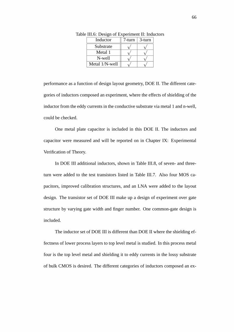
III.5 Device Design of Experiment . . . . . . . . . . . . . . . . . . . . . . . . . . . . . 65
III.6 Summary . . . . . . . . . . . . . . . . . . . . . . . . . . . . . . . . . . . . . . . . . . . . . . 69
IV Linearity Analysis of MOSFET’s . . . . . . . . . . . . . . . . . . . . . . . . . . . . . . . . 70
IV.1 Introduction . . . . . . . . . . . . . . . . . . . . . . . . . . . . . . . . . . . . . . . . . . . 70
IV.2 Grounded-Source Nonlinear Transfer Function of Output Circuit 74
IV.2.1 Grounded-Source Nonlinear Transfer Function of Input Cir-
cuit . . . . . . . . . . . . . . . . . . . . . . . . . . . . . . . . . . . . . . . . . . . . . . . . 77
IV.2.2 Total Nonlinear Transfer Function . . . . . . . . . . . . . . . . . . . . . . 81
IV.2.3 Third-Order Intermodulation Distortion in Volterra Trans-
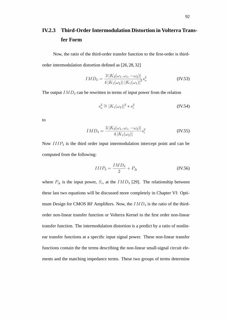
fer Form. . . . . . . . . . . . . . . . . . . . . . . . . . . . . . . . . . . . . . . . . . . . 92
IV.3 The Effect of Shunt Feedback on Linearity . . . . . . . . . . . . . . . . . . 93
IV.4 Predictions of Linearity . . . . . . . . . . . . . . . . . . . . . . . . . . . . . . . . . . 99
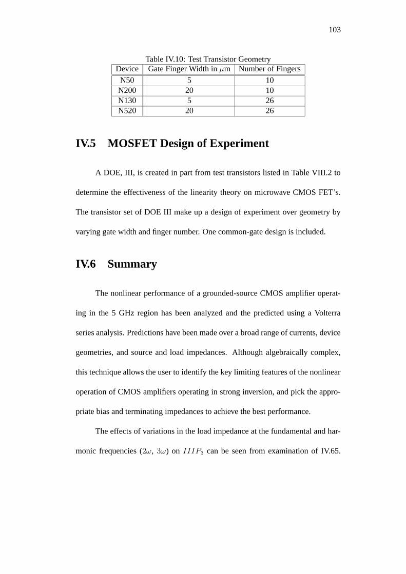
IV.5 MOSFET Design of Experiment . . . . . . . . . . . . . . . . . . . . . . . . . . 103
IV.6 Summary . . . . . . . . . . . . . . . . . . . . . . . . . . . . . . . . . . . . . . . . . . . . . . 103
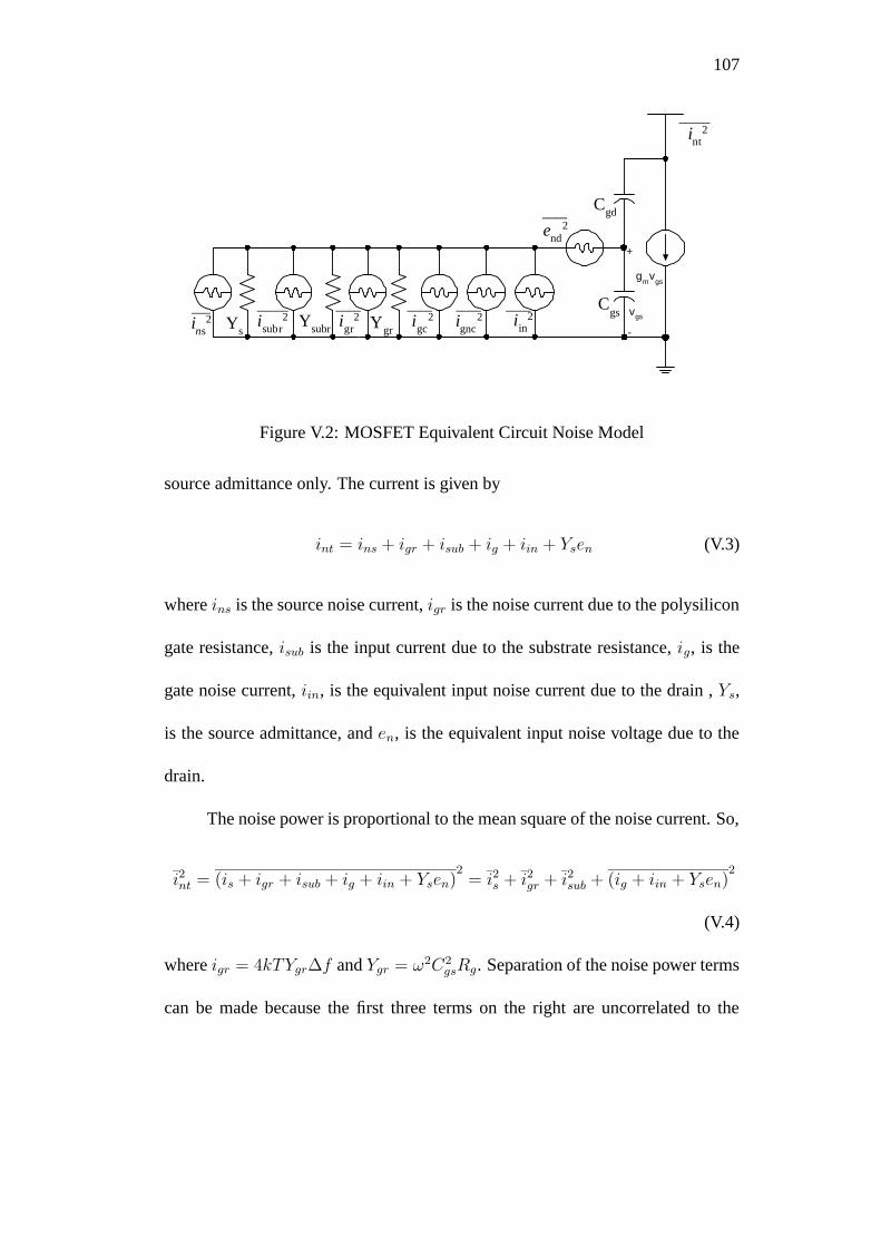
V Noise Analysis of CMOS FET’s . . . . . . . . . . . . . . . . . . . . . . . . . . . . . . . . . 105
V.1 Introduction . . . . . . . . . . . . . . . . . . . . . . . . . . . . . . . . . . . . . . . . . . . 105
V.2 Noise Figure Analysis . . . . . . . . . . . . . . . . . . . . . . . . . . . . . . . . . . . 106
V.3 Minimum Noise Figure with Feedback . . . . . . . . . . . . . . . . . . . . . 111
V.4 Minimum Noise Figure Predictions without and with Feedback 114
V.4.1 Noise Theory Predictions without feedback . . . . . . . . . . . . . . 114
V.4.2 Noise Theory Predictions with feedback . . . . . . . . . . . . . . . . . 114
V.5 Summary . . . . . . . . . . . . . . . . . . . . . . . . . . . . . . . . . . . . . . . . . . . . . . 116
vi
Page 7
VI Optimum Design for CMOS RF Amplifiers . . . . . . . . . . . . . . . . . . . . . . . 118
VI.1 Introduction to Optimum RF Design Techniques . . . . . . . . . . . . . 118
VI.2 Optimizing CMOS Amplifier Stability . . . . . . . . . . . . . . . . . . . . . 119
VI.3 Optimization of Impedance Termination Matching for CMOS
Amplifiers . . . . . . . . . . . . . . . . . . . . . . . . . . . . . . . . . . . . . . . . . . . . . 121
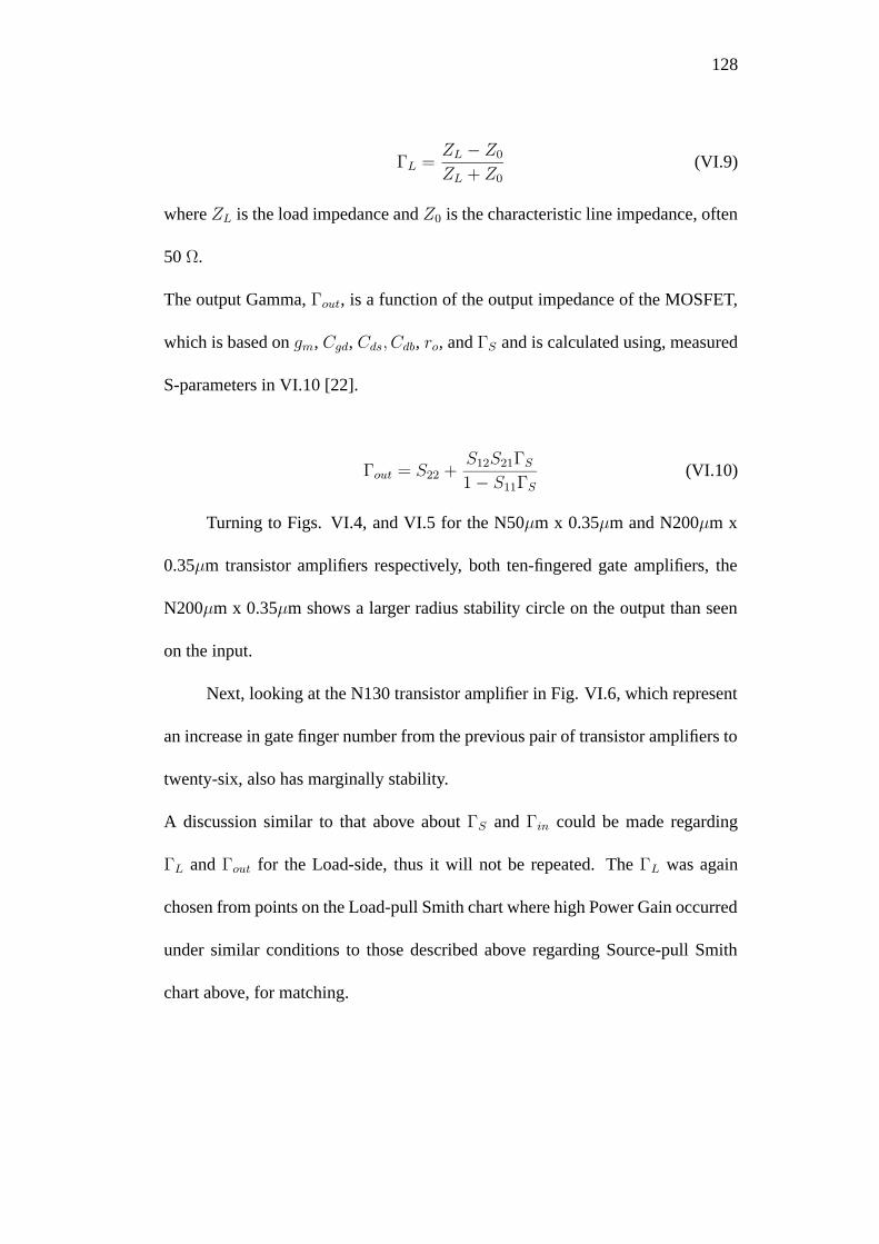
VI.3.1 Optimum Source Matching of CMOS Amplifiers . . . . . . . . . 121
VI.3.2 Load Side Matching . . . . . . . . . . . . . . . . . . . . . . . . . . . . . . . . . . 126
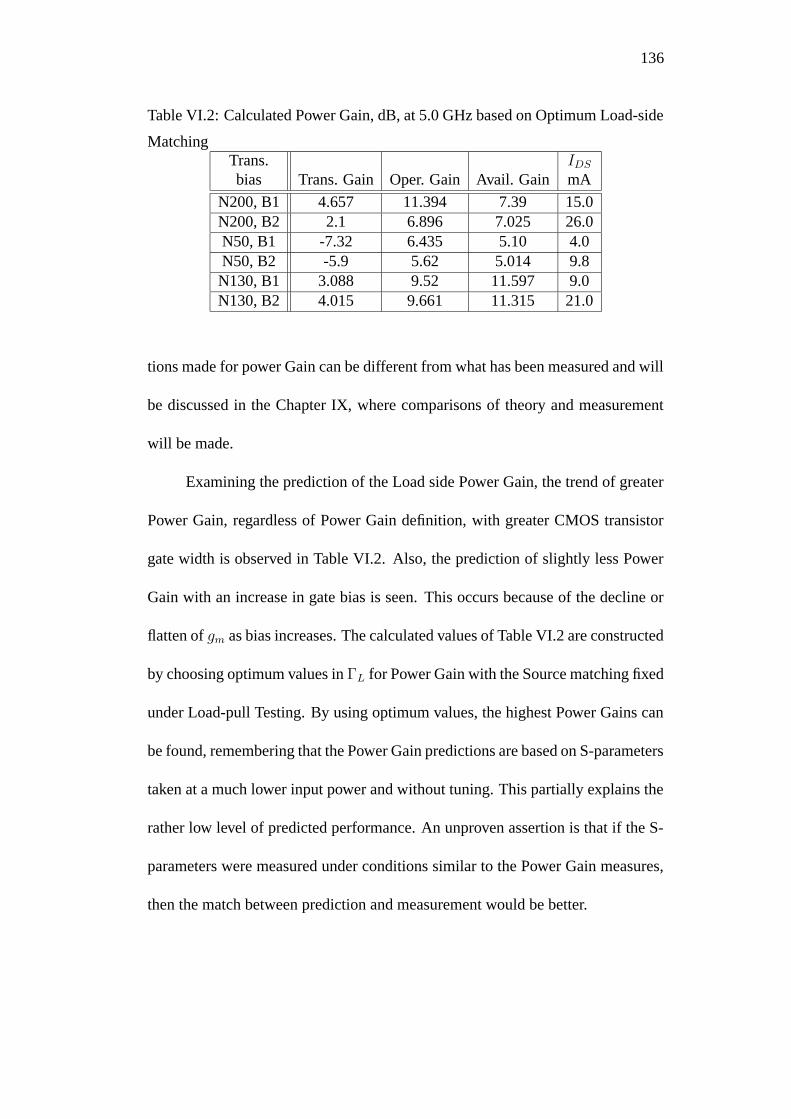
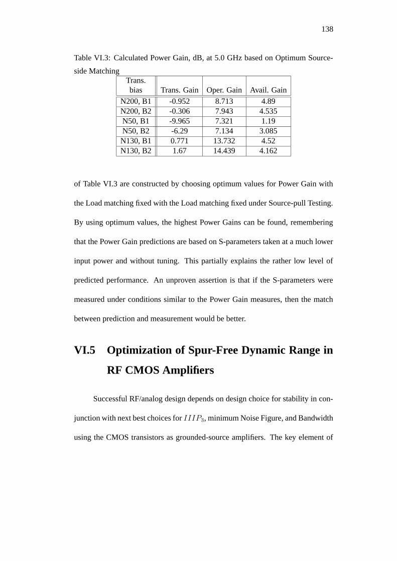
VI.4 Power Gain Theory of CMOS Amplifiers . . . . . . . . . . . . . . . . . . . 132
VI.4.1 Transducer Gain . . . . . . . . . . . . . . . . . . . . . . . . . . . . . . . . . . . . . 133
VI.4.2 Operating Power Gain . . . . . . . . . . . . . . . . . . . . . . . . . . . . . . . . 133
VI.4.3 Available Power Gain . . . . . . . . . . . . . . . . . . . . . . . . . . . . . . . . 134
VI.4.4 RF Power Gain Predictions . . . . . . . . . . . . . . . . . . . . . . . . . . . . 135
VI.5 Optimization of Spur-Free Dynamic Range in RF CMOS Am-
plifiers . . . . . . . . . . . . . . . . . . . . . . . . . . . . . . . . . . . . . . . . . . . . . . . . 138
VI.5.1 Optimum Dynamic Range Scaling . . . . . . . . . . . . . . . . . . . . . . 140
VI.5.2 Optimum Dynamic Range Scaling Predictions . . . . . . . . . . . . 142
VI.5.3 SFDR RF CMOS Amplifier Design Optimization Predictions145
VI.5.4 Summary of Optimum Dynamic Range Scaling . . . . . . . . . . . 145
VI.6 Summary . . . . . . . . . . . . . . . . . . . . . . . . . . . . . . . . . . . . . . . . . . . . . . 147
VII LNA Design . . . . . . . . . . . . . . . . . . . . . . . . . . . . . . . . . . . . . . . . . . . . . . . . . 148
VII.1 Introduction to LNA Design . . . . . . . . . . . . . . . . . . . . . . . . . . . . . . 148
VII.2 LNA for 5.0 GHz IMS Application . . . . . . . . . . . . . . . . . . . . . . . . 148
VII.2.1 5.0 GHz LNA Design Goals . . . . . . . . . . . . . . . . . . . . . . . . . . . 149
VII.2.2 Design, Simulation, and Layout of 5.0 GHz LNA . . . . . . . . . 150
VII.3 Millimeter wave 26.0 GHz LNA . . . . . . . . . . . . . . . . . . . . . . . . . . 155
VII.3.1 Design Goals for 26.0 GHz LNA . . . . . . . . . . . . . . . . . . . . . . . 155
VII.3.2 Design, Simulation, and Layout of 26.0 GHz LNA . . . . . . . . 156
VII.4 LNA Summary . . . . . . . . . . . . . . . . . . . . . . . . . . . . . . . . . . . . . . . . . 160
VIII Laboratory Experiment and Test Engineering . . . . . . . . . . . . . . . . . . . . . . 161
VIII.1 Introduction . . . . . . . . . . . . . . . . . . . . . . . . . . . . . . . . . . . . . . . . . . . 161
VIII.2 Design of Experiment . . . . . . . . . . . . . . . . . . . . . . . . . . . . . . . . . . . 162
VIII.2.1 Layouts Submitted for Experimental Verification . . . . . . . . . . 162
VIII.2.2 Design of Experiment . . . . . . . . . . . . . . . . . . . . . . . . . . . . . . . . 163
VIII.3 DC Measurement . . . . . . . . . . . . . . . . . . . . . . . . . . . . . . . . . . . . . . . 166
vii
Page 8
VIII.4 Small-Signal Measurement . . . . . . . . . . . . . . . . . . . . . . . . . . . . . . . 167
VIII.4.1 S-Parameter Measurement . . . . . . . . . . . . . . . . . . . . . . . . . . . . 168
VIII.4.2 Load-Pull Measurement System . . . . . . . . . . . . . . . . . . . . . . . . 172
VIII.4.3 Noise Measurement . . . . . . . . . . . . . . . . . . . . . . . . . . . . . . . . . . 175
VIII.5 Summary . . . . . . . . . . . . . . . . . . . . . . . . . . . . . . . . . . . . . . . . . . . . . . 180
IX Experimental Verification of Theory . . . . . . . . . . . . . . . . . . . . . . . . . . . . . . 181
IX.1 Introduction to Experimental Verification . . . . . . . . . . . . . . . . . . . 181
IX.2 Device Modelling Results . . . . . . . . . . . . . . . . . . . . . . . . . . . . . . . . 181
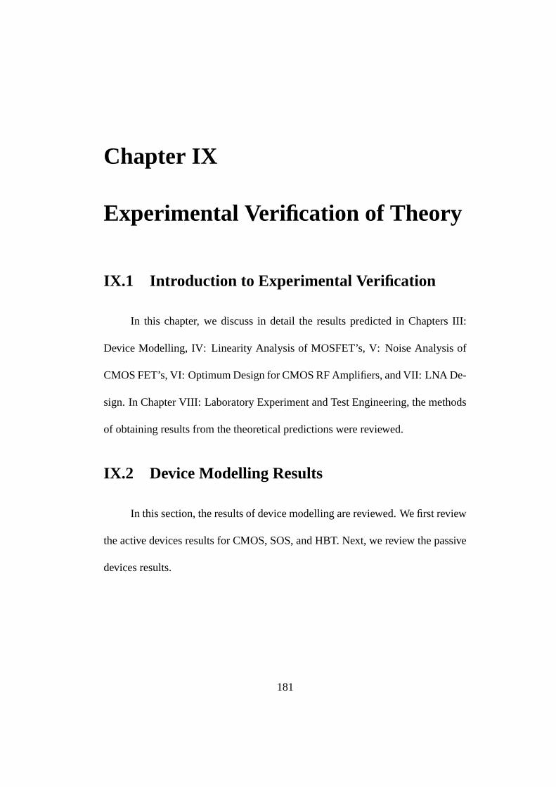
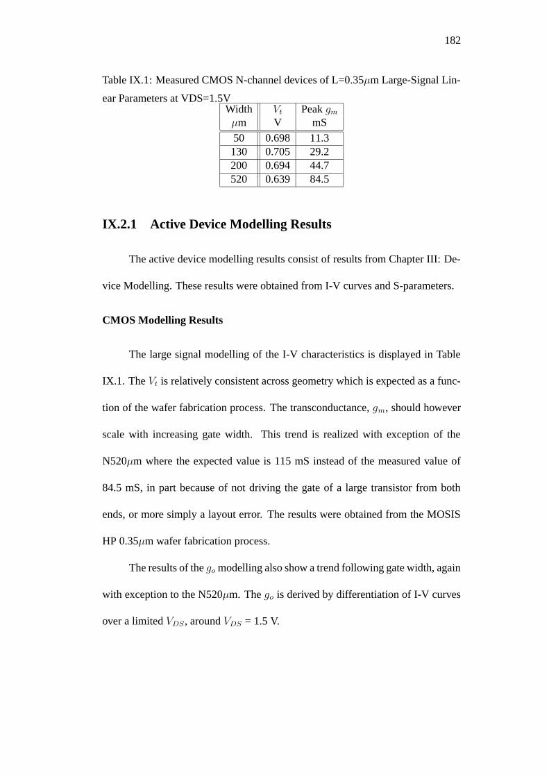
IX.2.1 Active Device Modelling Results . . . . . . . . . . . . . . . . . . . . . . . 182
IX.2.2 Passive Device Modelling Results . . . . . . . . . . . . . . . . . . . . . . 202
IX.3 Test Results for Linearity Analysis of MOSFET’s–Comparison
of Theory and Results . . . . . . . . . . . . . . . . . . . . . . . . . . . . . . . . . . . 203
IX.4 Test Results for Noise Analysis of CMOS FET’s . . . . . . . . . . . . . 205
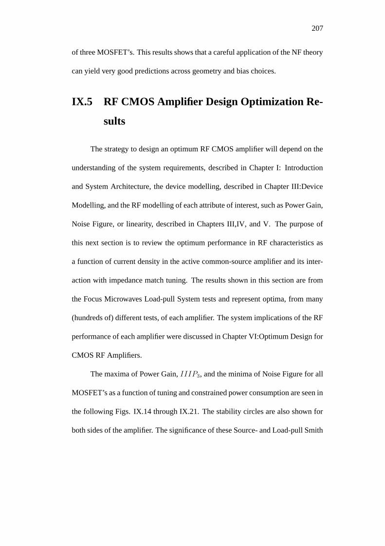
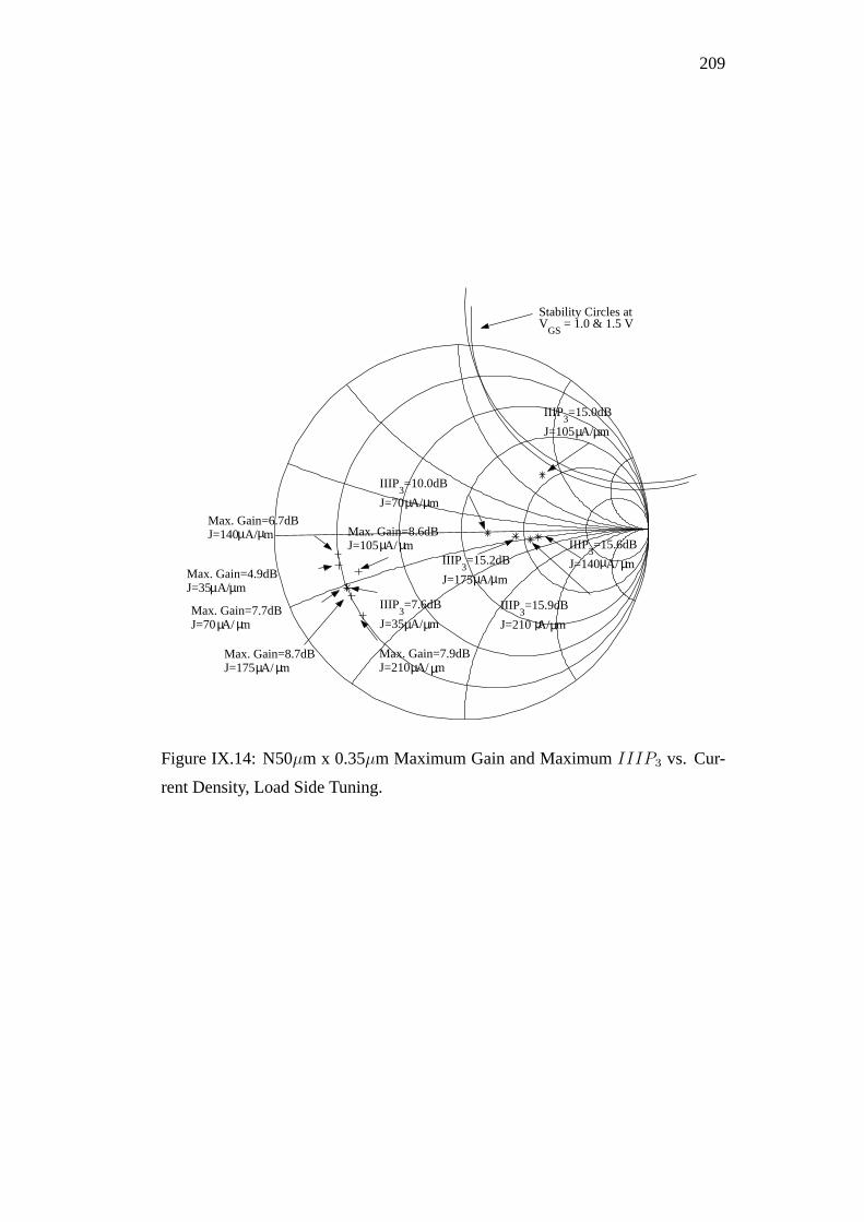
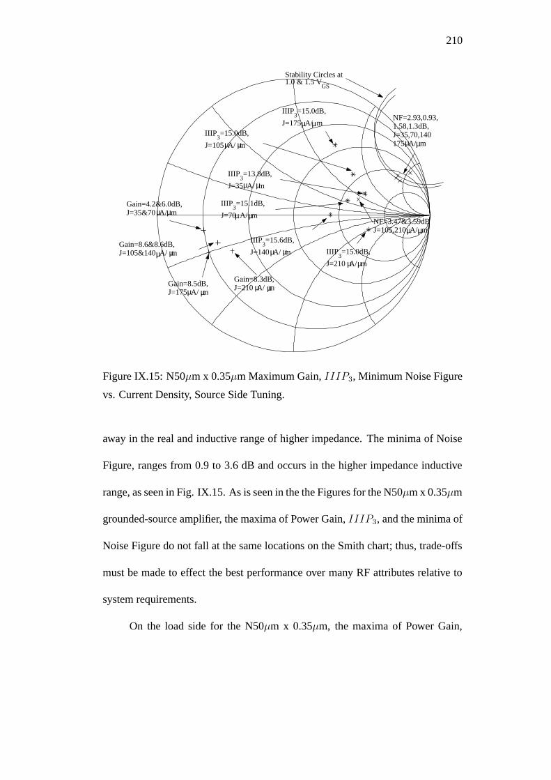
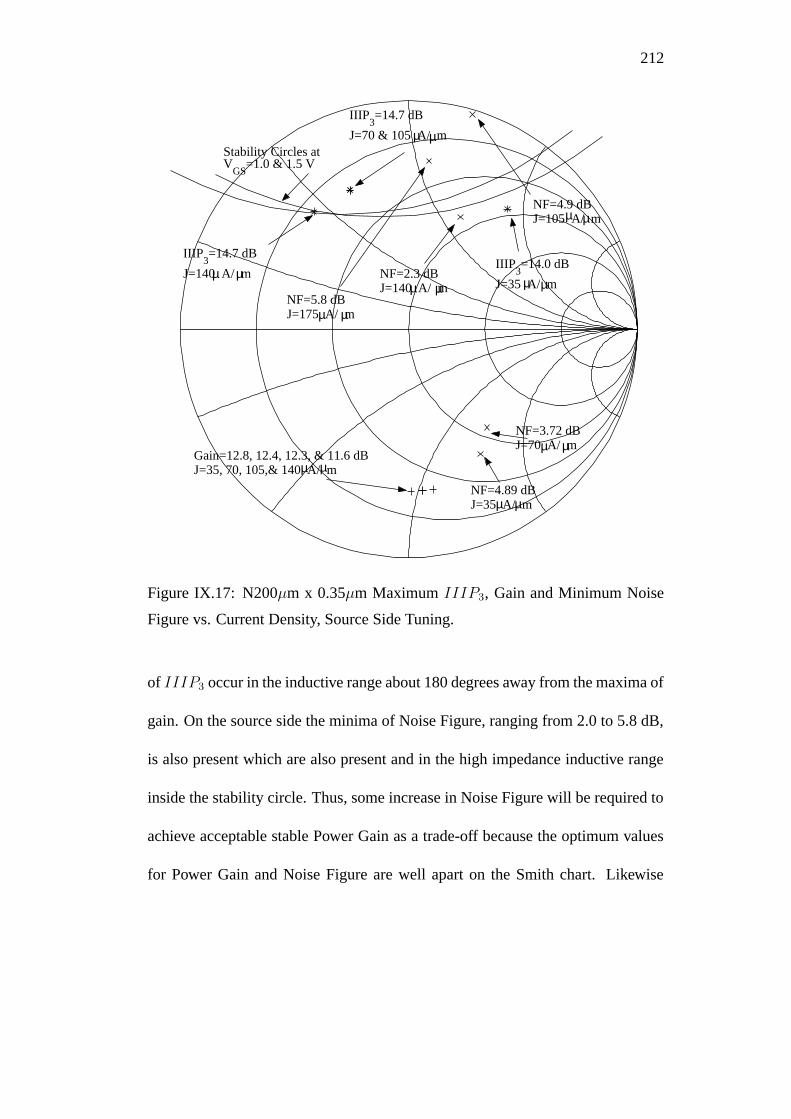
IX.5 RF CMOS Amplifier Design Optimization Results . . . . . . . . . . . 207
IX.6 LNA Design Results . . . . . . . . . . . . . . . . . . . . . . . . . . . . . . . . . . . . 218
IX.7 Summary . . . . . . . . . . . . . . . . . . . . . . . . . . . . . . . . . . . . . . . . . . . . . . 221
X Conclusion . . . . . . . . . . . . . . . . . . . . . . . . . . . . . . . . . . . . . . . . . . . . . . . . . . . 223
X.1 Research Summary . . . . . . . . . . . . . . . . . . . . . . . . . . . . . . . . . . . . . 223
X.2 Future Research Outlook . . . . . . . . . . . . . . . . . . . . . . . . . . . . . . . . . 227
Bibliography . . . . . . . . . . . . . . . . . . . . . . . . . . . . . . . . . . . . . . . . . . . . . . . . . 229
viii
Page 9
LIST OF FIGURES
I.1 RF System Block Diagram . . . . . . . . . . . . . . . . . . . . . . . . . . . . . . . 2
I.2 Bit Error Probability vs. Eb/No . . . . . . . . . . . . . . . . . . . . . . . . . . . . 6
I.3 16 QAM Constellation . . . . . . . . . . . . . . . . . . . . . . . . . . . . . . . . . . . 8
II.1 ISM Receiver . . . . . . . . . . . . . . . . . . . . . . . . . . . . . . . . . . . . . . . . . . . 17
II.2 Microwave Common Source Amplifier . . . . . . . . . . . . . . . . . . . . . 19
II.3 RF Radio System . . . . . . . . . . . . . . . . . . . . . . . . . . . . . . . . . . . . . . . 20
III.1 Bulk NMOS Transistor Physical Diagram [1] . . . . . . . . . . . . . . . . 24
III.2 SOI NMOS Transistor Physical Diagram [2] . . . . . . . . . . . . . . . . . 27
III.3 Heterojunction Bipolar Transistor Physical Diagram [3] . . . . . . . 28
III.4 N50µm x 0.35µm Large-Signal Current vs. Voltage, VDS = 1.5V . 29
III.5 N130µm x 0.35µm Large-Signal Current vs. Voltage, Linear
Region, VDS = 1.5V . . . . . . . . . . . . . . . . . . . . . . . . . . . . . . . . . . . . . 30
III.6 N200µm x 0.35µm Large-Signal Current vs. Voltage, VDS =
1.5V . . . . . . . . . . . . . . . . . . . . . . . . . . . . . . . . . . . . . . . . . . . . . . . . . . 31
III.7 N520µm x 0.35µm Large-Signal Current vs. Voltage, VDS =
1.5V . . . . . . . . . . . . . . . . . . . . . . . . . . . . . . . . . . . . . . . . . . . . . . . . . . 31
III.8 N50µm x 0.35µm Large-Signal Current vs. Voltage, 1.0V ≤VGS ≤ 3.0V . . . . . . . . . . . . . . . . . . . . . . . . . . . . . . . . . . . . . . . . . . . . 32
III.9 N130µm x 0.35µm Large-Signal Current vs. Voltage, 1.0V ≤VGS ≤ 3.0V . . . . . . . . . . . . . . . . . . . . . . . . . . . . . . . . . . . . . . . . . . . . 33
III.10 N200µm x 0.35µm Large-Signal Current vs. Voltage, 0.0V ≤VGS ≤ 3.0V . . . . . . . . . . . . . . . . . . . . . . . . . . . . . . . . . . . . . . . . . . . . 33
III.11 N520µm x 0.35µm Large-Signal Current vs. Voltage, 0.3V ≤VGS ≤ 1.5V . . . . . . . . . . . . . . . . . . . . . . . . . . . . . . . . . . . . . . . . . . . . 34
III.12 Simplified small-signal MOSFET model equivalent circuit show-
ing sources of nonlinear distortion. . . . . . . . . . . . . . . . . . . . . . . . . . 35
III.13 Two Port S-Parameter Measurement Model . . . . . . . . . . . . . . . . . . 36
III.14 N50µm x 0.35µm Measured and Modelled gm vs. VGS . . . . . . . . 40
III.15 N130µm x 0.35µm Measured and Modelled gm vs. VGS . . . . . . . 41
III.16 N200µm x 0.35µm Measured and Modelled gm vs. VGS . . . . . . . 42
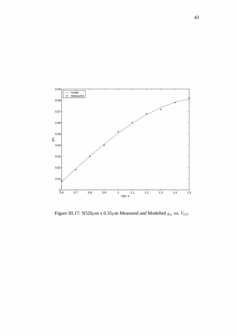
III.17 N520µm x 0.35µm Measured and Modelled gm vs. VGS . . . . . . . 43
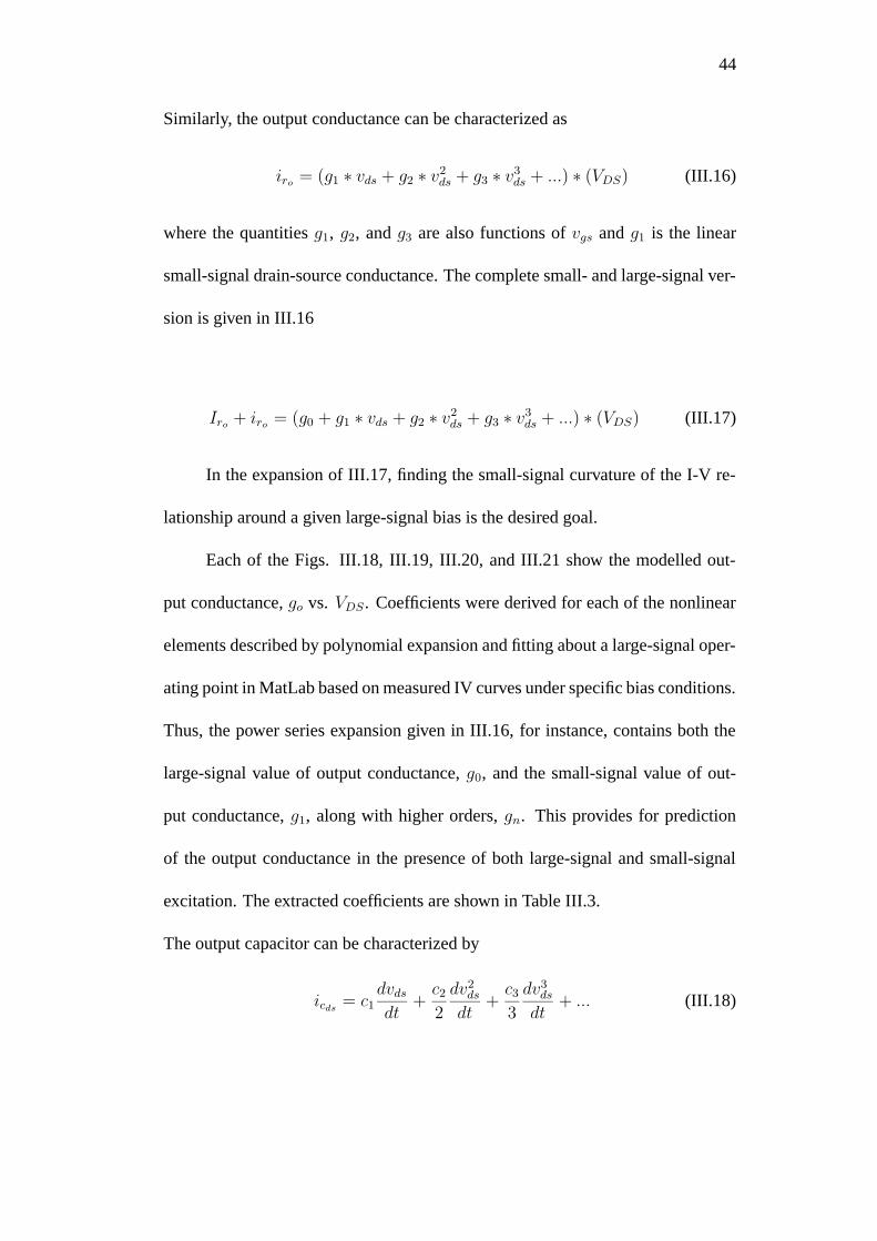
III.18 N50µm x 0.35µm Measured and Modelled go vs. VDS . . . . . . . . 45
ix
Page 10
III.19 N130µm x 0.35µm Measured and Modelled go vs. VDS . . . . . . . 46
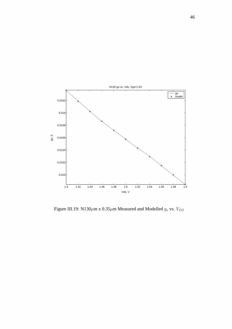
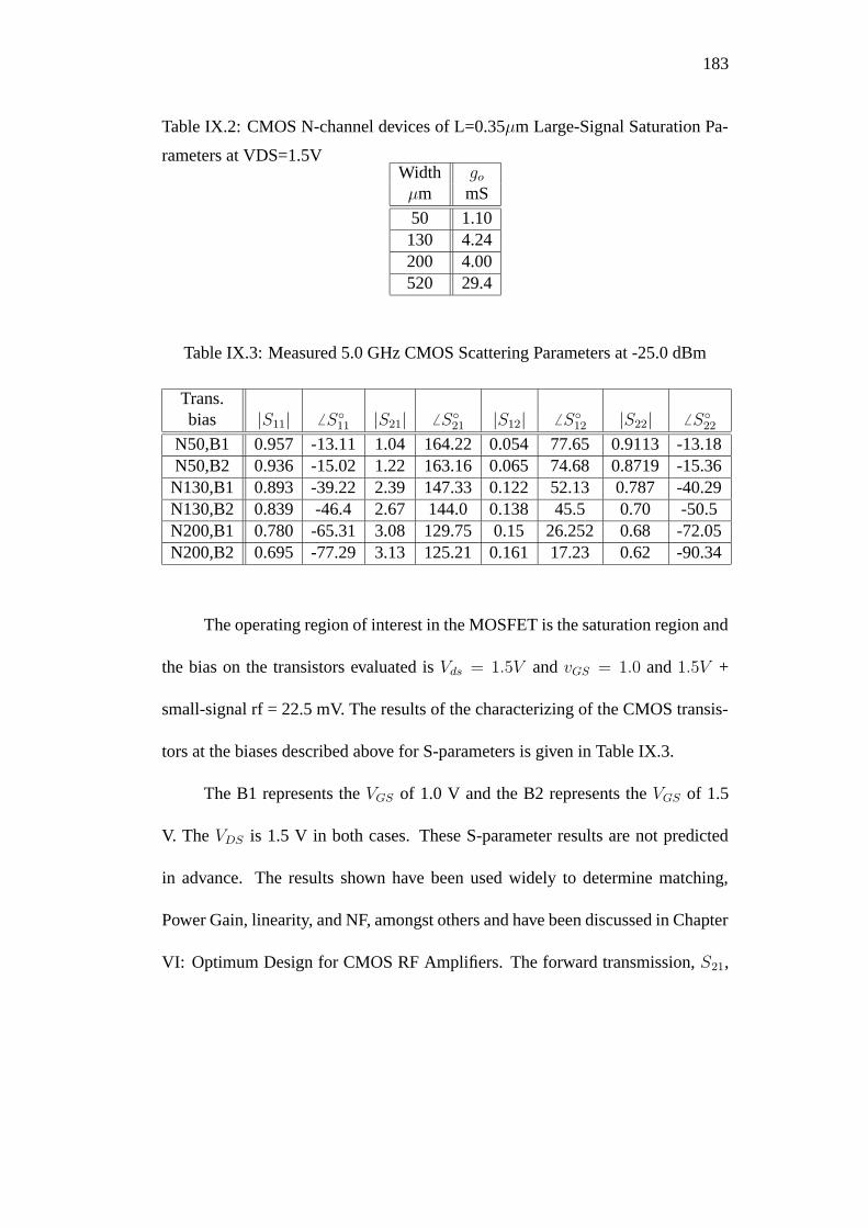
III.20 N200µm x 0.35µm Measured and Modelled go vs. VDS . . . . . . . 47
III.21 N520µm x 0.35µm Measured and Modelled go vs. VDS . . . . . . . 48
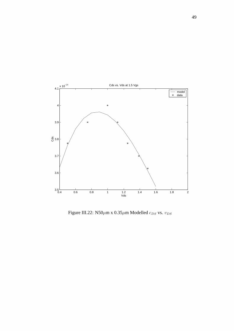
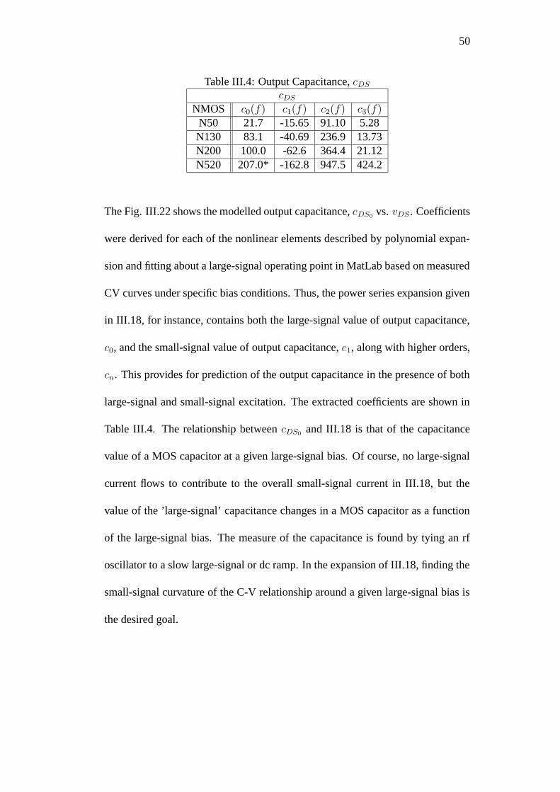
III.22 N50µm x 0.35µm Modelled cDS vs. vDS . . . . . . . . . . . . . . . . . . . . 49
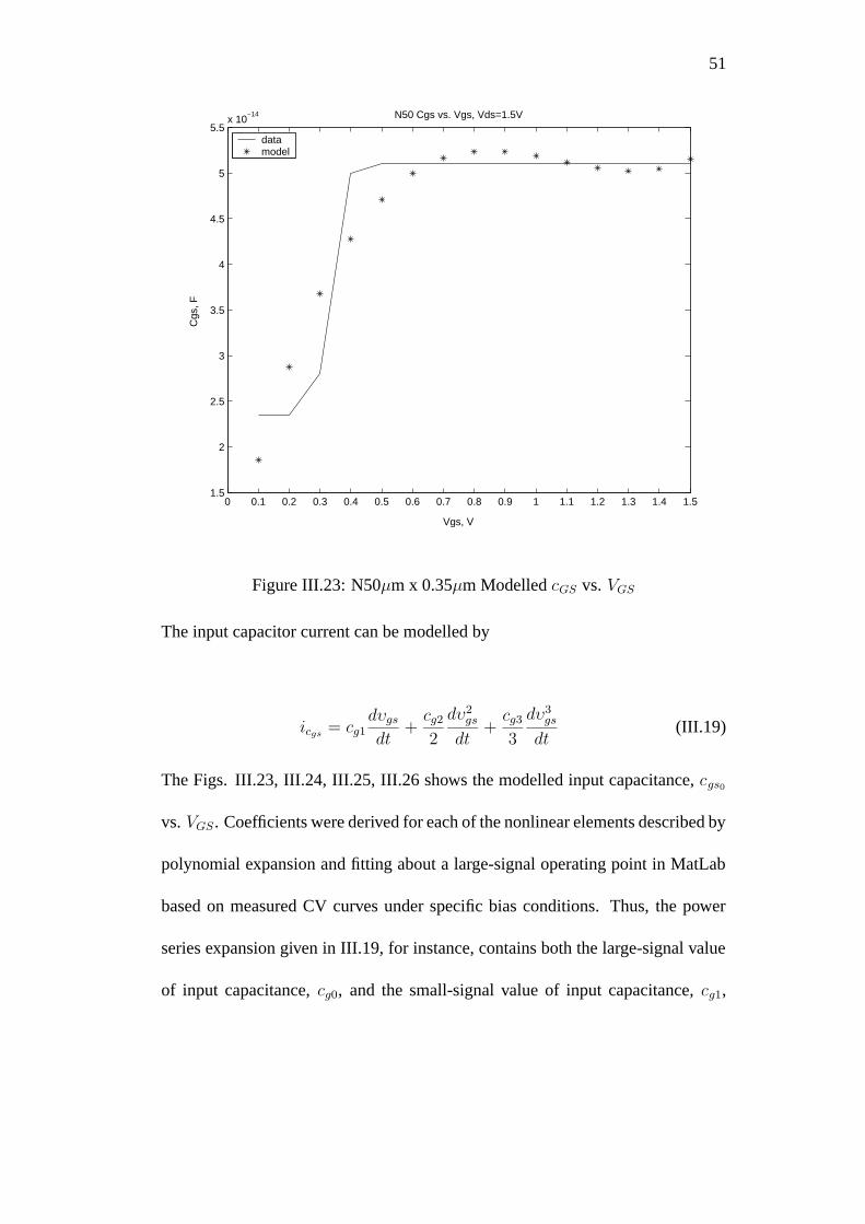
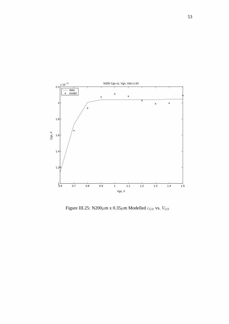
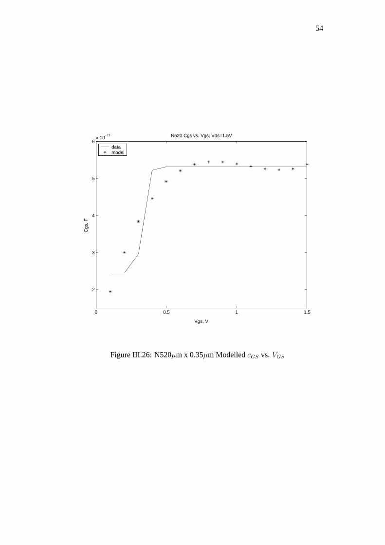
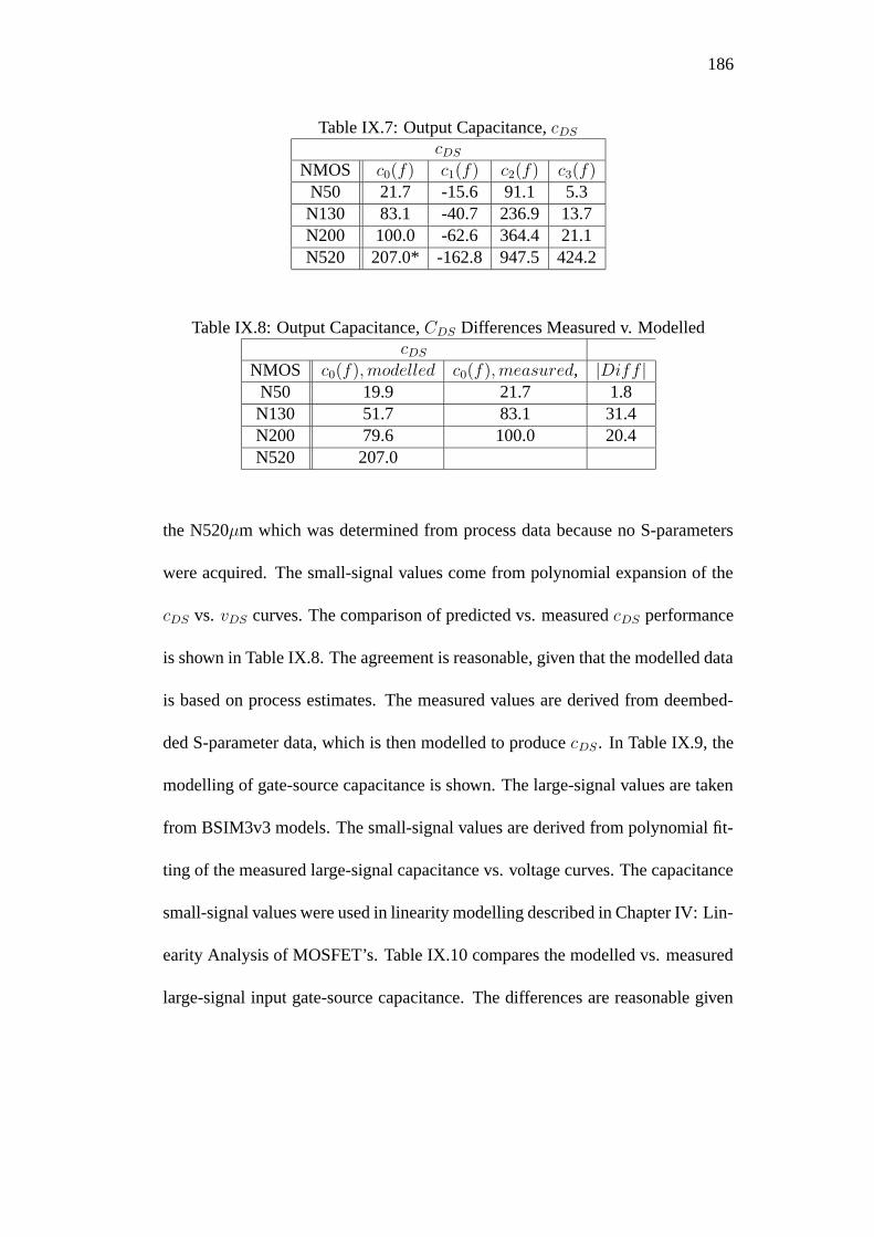
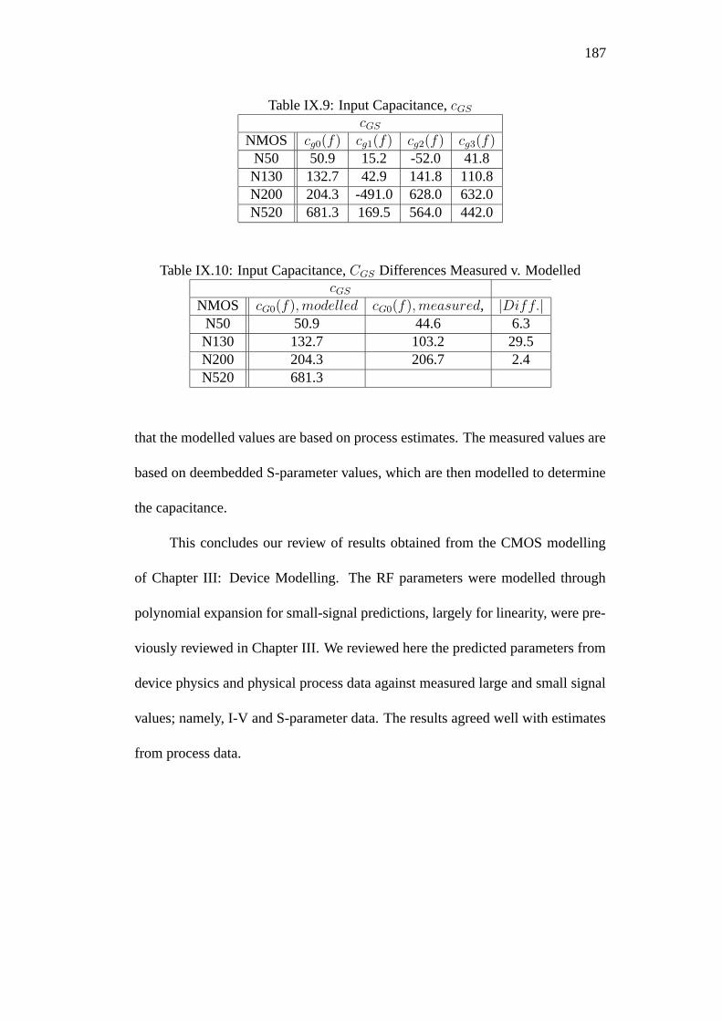
III.23 N50µm x 0.35µm Modelled cGS vs. VGS . . . . . . . . . . . . . . . . . . . . 51
III.24 N130µm x 0.35µm Modelled cGS vs. VGS . . . . . . . . . . . . . . . . . . . 52
III.25 N200µm x 0.35µm Modelled cGS vs. VGS . . . . . . . . . . . . . . . . . . . 53
III.26 N520µm x 0.35µm Modelled cGS vs. VGS . . . . . . . . . . . . . . . . . . . 54
III.27 The Converted Cadence Spectre Transistor Model of AT’s HSPICE
BSIM3v3 . . . . . . . . . . . . . . . . . . . . . . . . . . . . . . . . . . . . . . . . . . . . . 57
III.28 2nd Part of The Converted Cadence Spectre Transistor Model
of AT’s HSPICE BSIM3v3 . . . . . . . . . . . . . . . . . . . . . . . . . . . . . . 58
III.29 IBM SOS Transistor Simulation Model . . . . . . . . . . . . . . . . . . . . . 58
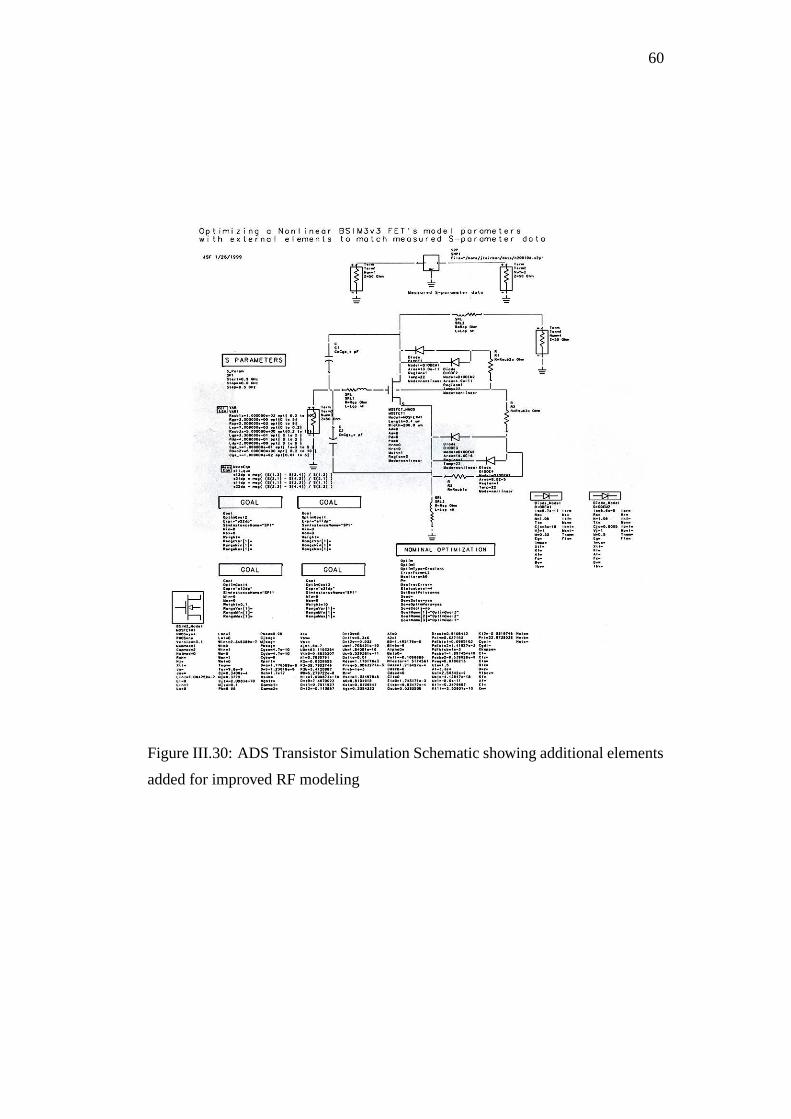
III.30 ADS Transistor Simulation Schematic showing additional ele-
ments added for improved RF modeling . . . . . . . . . . . . . . . . . . . . 60
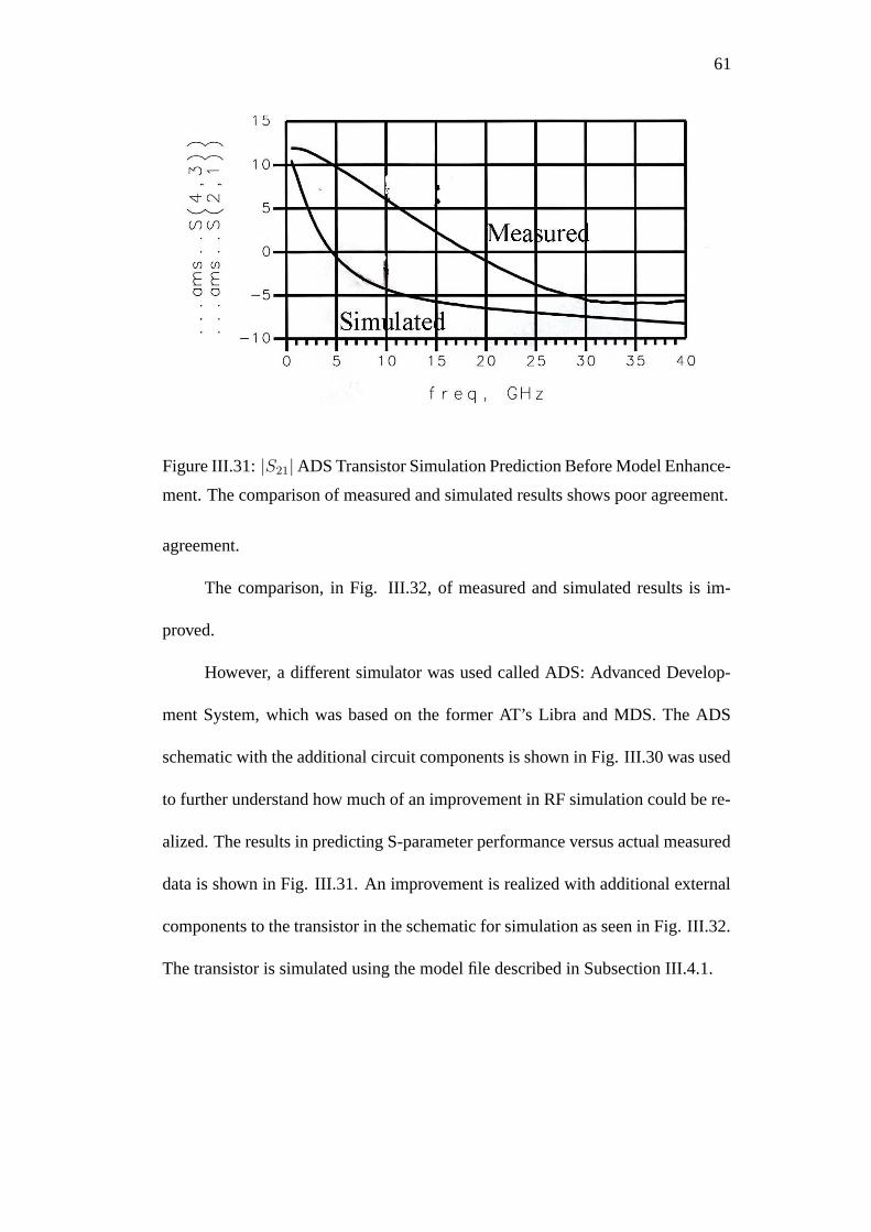
III.31 |S21| ADS Transistor Simulation Prediction Before Model En-
hancement. The comparison of measured and simulated results
shows poor agreement. . . . . . . . . . . . . . . . . . . . . . . . . . . . . . . . . . . . 61
III.32 Polar plot of |S21| ADS Transistor Simulation Prediction after
Model Enhancement. . . . . . . . . . . . . . . . . . . . . . . . . . . . . . . . . . . . . 62
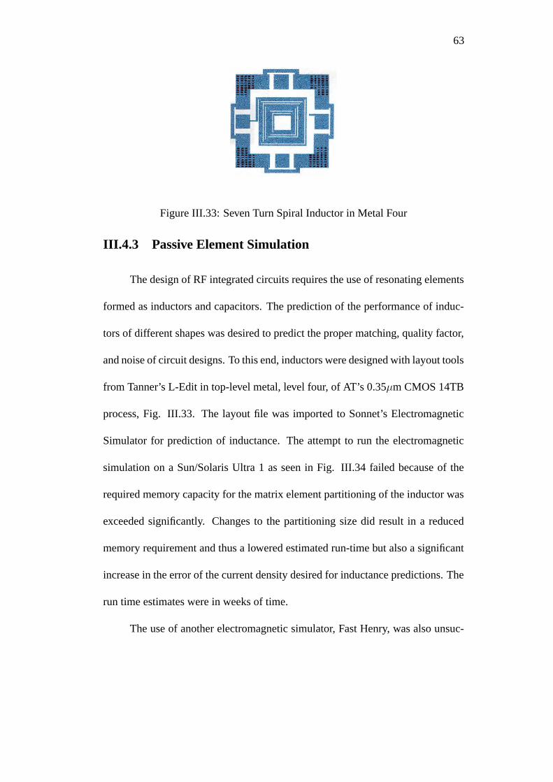
III.33 Seven Turn Spiral Inductor in Metal Four . . . . . . . . . . . . . . . . . . . 63
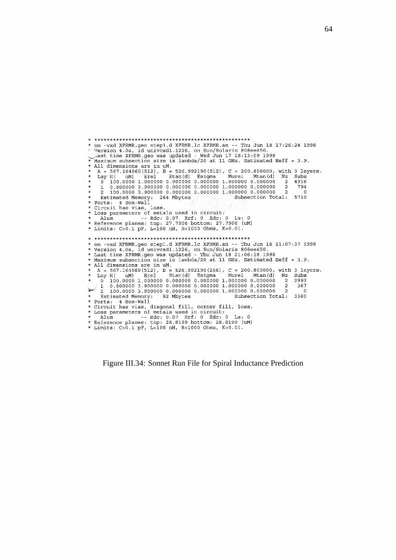
III.34 Sonnet Run File for Spiral Inductance Prediction . . . . . . . . . . . . . 64
IV.1 Weakly Nonlinear Block Diagram. . . . . . . . . . . . . . . . . . . . . . . . . . 72
IV.2 Simplified small-signal MOSFET model equivalent circuit show-
ing sources of nonlinear distortion. . . . . . . . . . . . . . . . . . . . . . . . . . 74
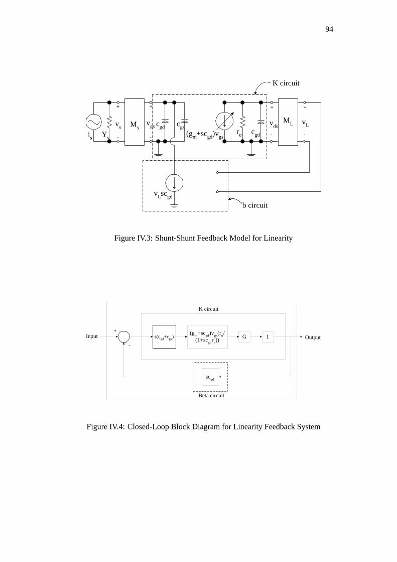
IV.3 Shunt-Shunt Feedback Model for Linearity . . . . . . . . . . . . . . . . . . 94
IV.4 Closed-Loop Block Diagram for Linearity Feedback System . . . 94
V.1 Two-Port Noise Model . . . . . . . . . . . . . . . . . . . . . . . . . . . . . . . . . . . 106
V.2 MOSFET Equivalent Circuit Noise Model . . . . . . . . . . . . . . . . . . 107
V.3 Smith Chart Showing Noise and Available Gain Circles . . . . . . . 117
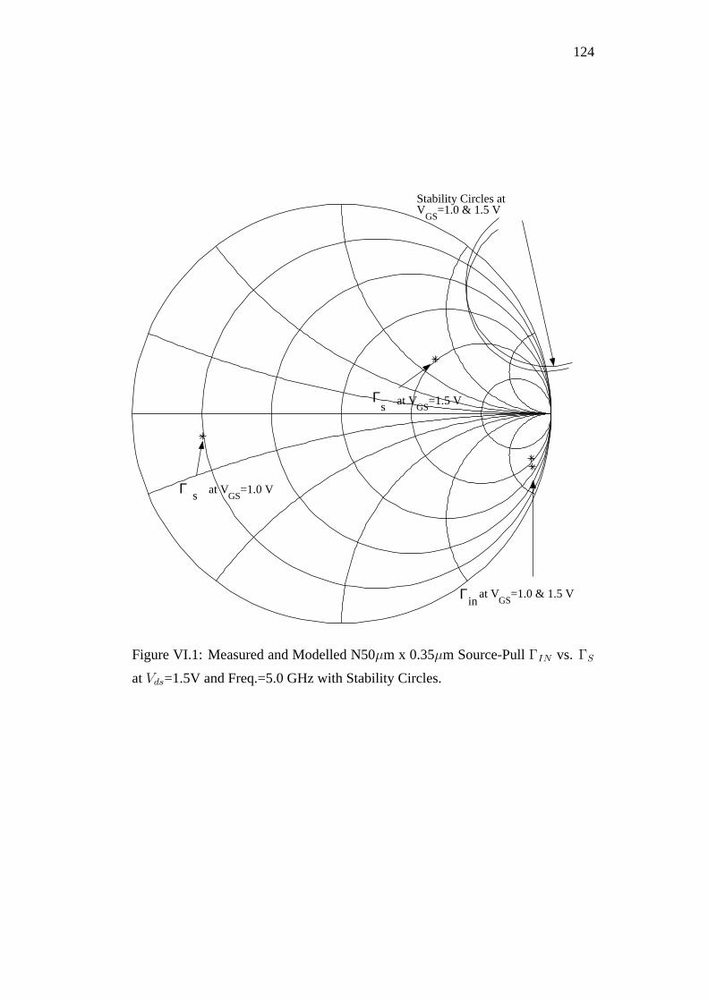
VI.1 Measured and Modelled N50µm x 0.35µm Source-Pull ΓIN vs.
ΓS at Vds=1.5V and Freq.=5.0 GHz with Stability Circles. . . . . . 124
x
Page 11
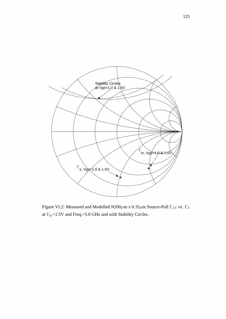
VI.2 Measured and Modelled N200µm x 0.35µm Source-Pull ΓIN
vs. ΓS at Vds=1.5V and Freq.=5.0 GHz and with Stability Circles.125
VI.3 Measured and Modelled N130 Source-Pull ΓIN vs. ΓS at Vds=1.5V
and Freq.=5.0 GHz with Stability Circles. . . . . . . . . . . . . . . . . . . . 127
VI.4 Measured and Modelled N50µm x 0.35µm Load-Pull ΓOUT vs.
ΓL at Vds=1.5V and Freq.=5.0 GHz with Stability Circles. . . . . . 129
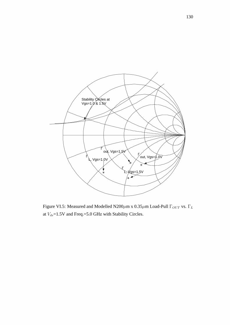
VI.5 Measured and Modelled N200µm x 0.35µm Load-Pull ΓOUT
vs. ΓL at Vds=1.5V and Freq.=5.0 GHz with Stability Circles. . . 130
VI.6 Measured and Modelled N130 Load-Pull ΓOUT vs. ΓL at Vds=1.5V
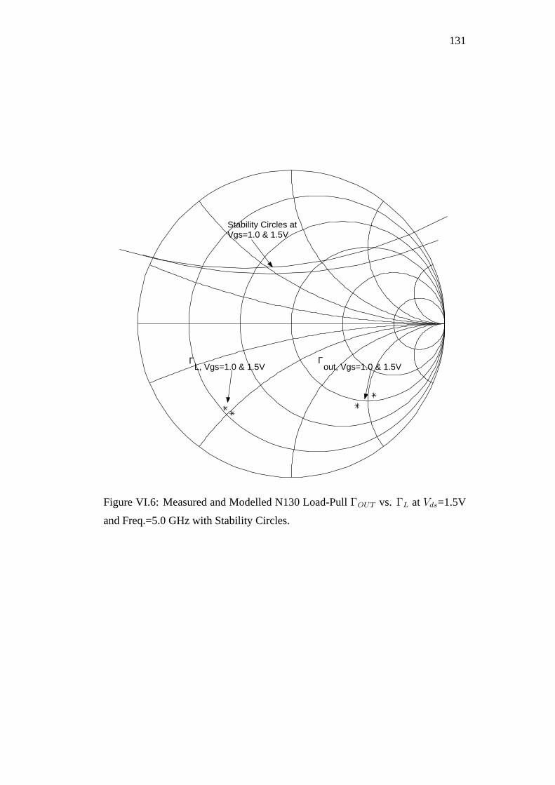
and Freq.=5.0 GHz with Stability Circles. . . . . . . . . . . . . . . . . . . . 131
VI.7 SFDR vs. Linearity. . . . . . . . . . . . . . . . . . . . . . . . . . . . . . . . . . . . . . 141
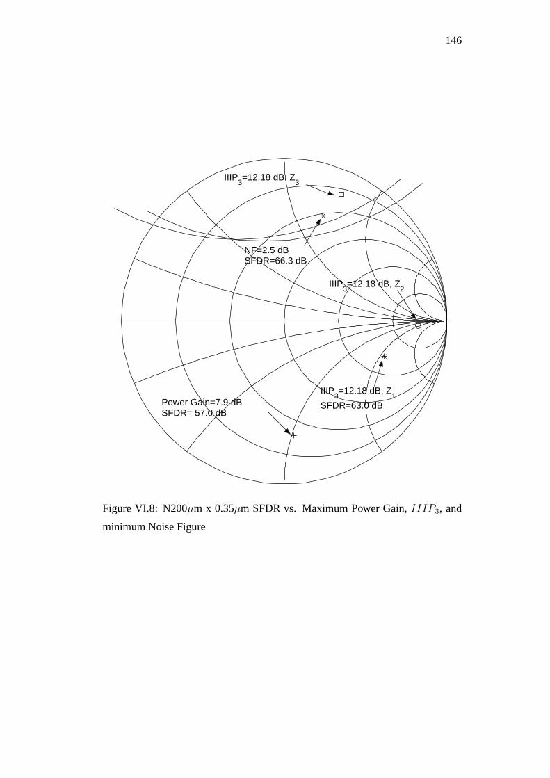
VI.8 N200µm x 0.35µm SFDR vs. Maximum Power Gain, IIIP3,
and minimum Noise Figure . . . . . . . . . . . . . . . . . . . . . . . . . . . . . . . 146
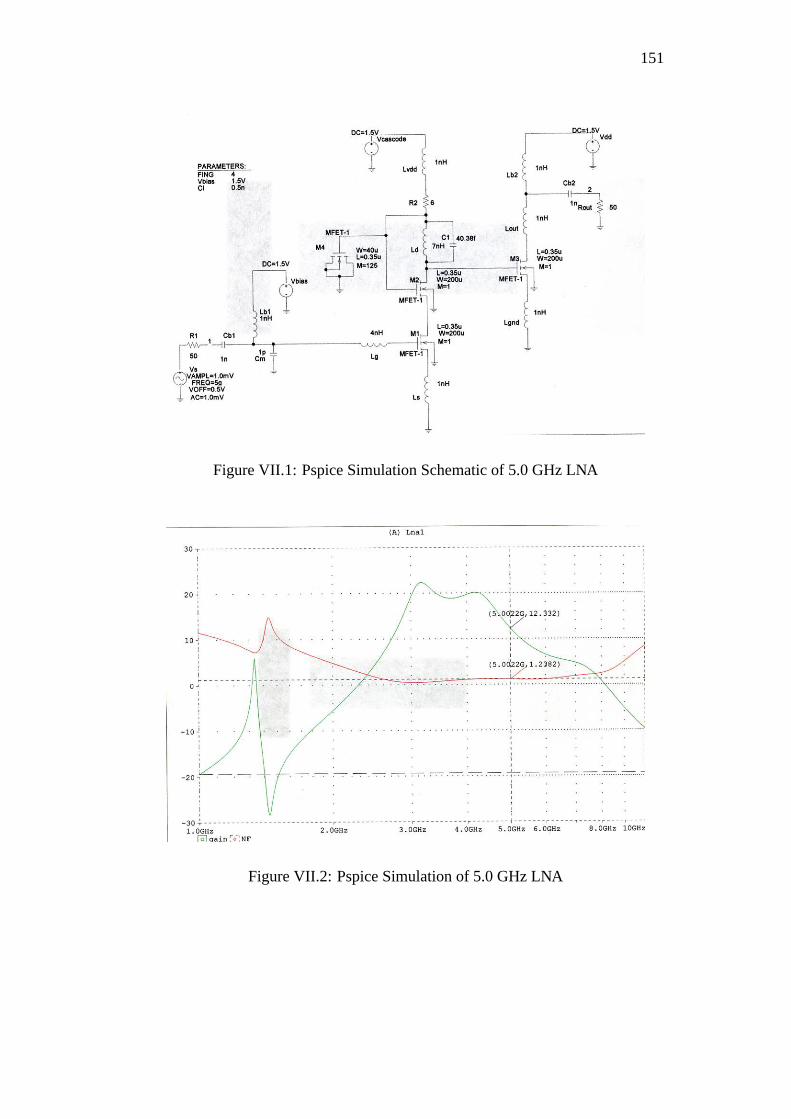
VII.1 Pspice Simulation Schematic of 5.0 GHz LNA . . . . . . . . . . . . . . . 151
VII.2 Pspice Simulation of 5.0 GHz LNA . . . . . . . . . . . . . . . . . . . . . . . . 151
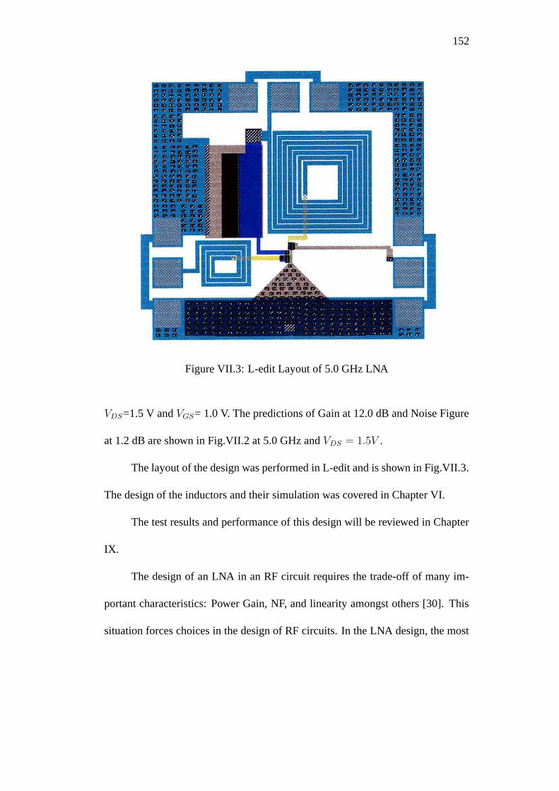
VII.3 L-edit Layout of 5.0 GHz LNA . . . . . . . . . . . . . . . . . . . . . . . . . . . . 152
VII.4 LNA Cascode MOSFET Circuit Model Including Impedance
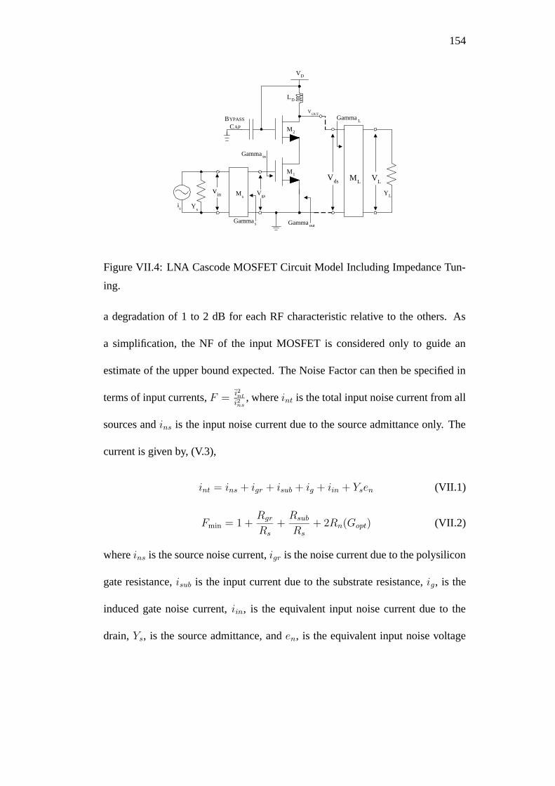
Tuning. . . . . . . . . . . . . . . . . . . . . . . . . . . . . . . . . . . . . . . . . . . . . . . . . 154
VII.5 Cadence Simulation Schematic of 26 GHz LNA showing gain
curve sweeps. . . . . . . . . . . . . . . . . . . . . . . . . . . . . . . . . . . . . . . . . . . 157
VII.6 Cadence Simulation of 26 GHz LNA . . . . . . . . . . . . . . . . . . . . . . . 157
VII.7 L-Edit Layout of 26 GHz LNA . . . . . . . . . . . . . . . . . . . . . . . . . . . . 158
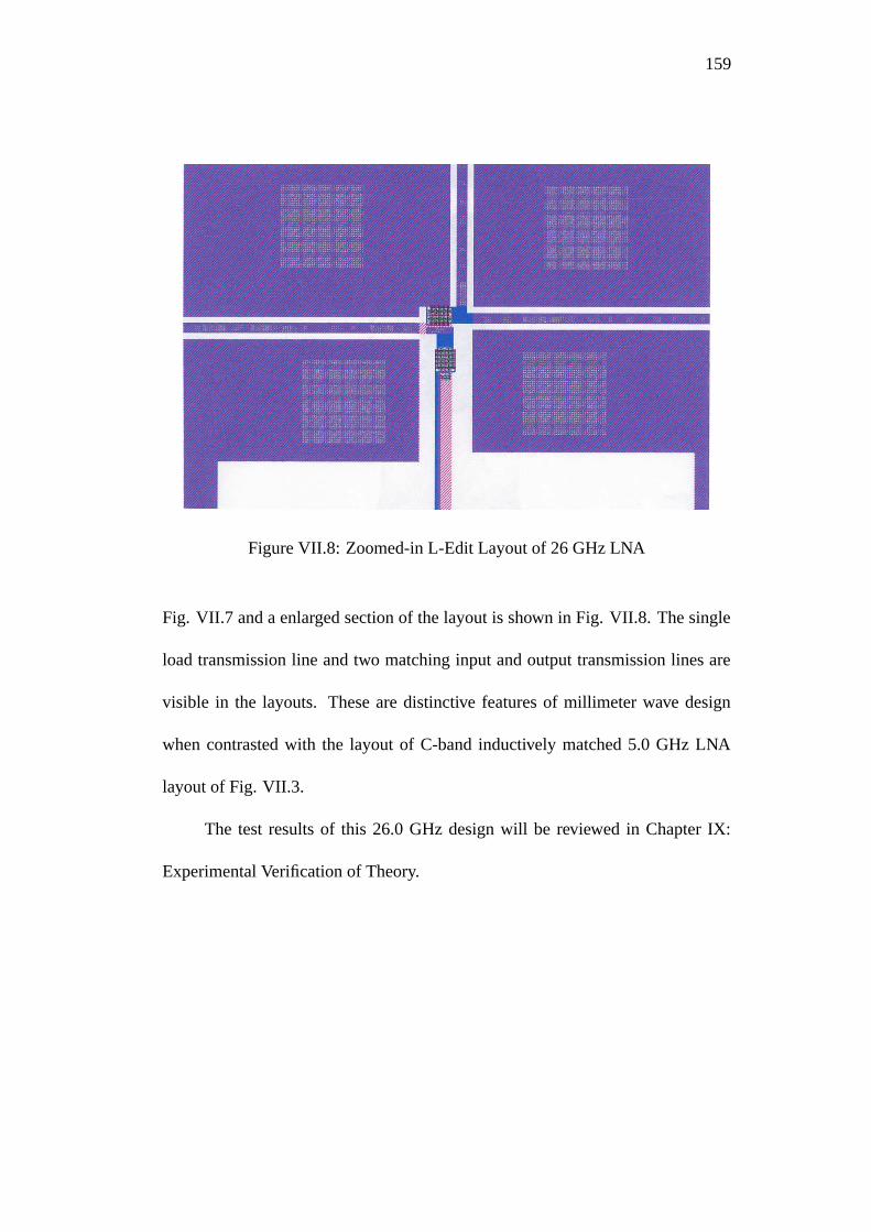
VII.8 Zoomed-in L-Edit Layout of 26 GHz LNA . . . . . . . . . . . . . . . . . . 159
VIII.1 Cascade Wafer Prober. . . . . . . . . . . . . . . . . . . . . . . . . . . . . . . . . . . . 167
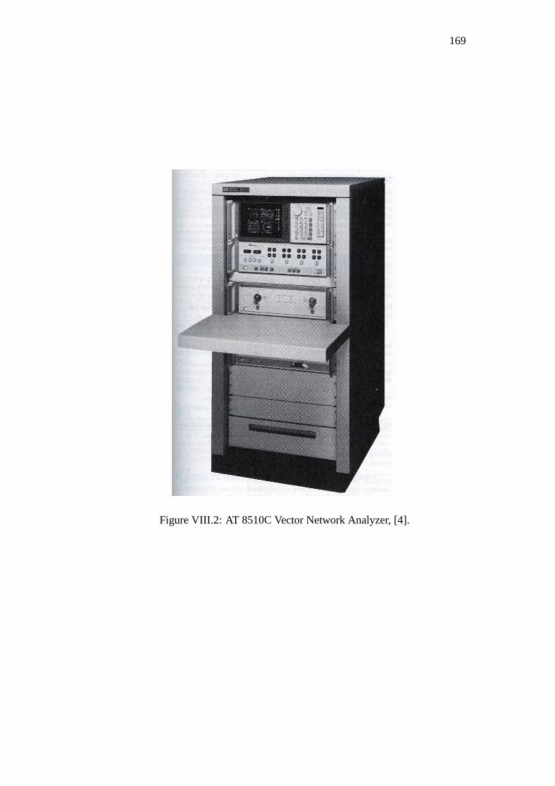
VIII.2 AT 8510C Vector Network Analyzer, [4]. . . . . . . . . . . . . . . . . . . . 169
VIII.3 Block Diagram of S-Parameter Measurement, [4]. . . . . . . . . . . . . 170
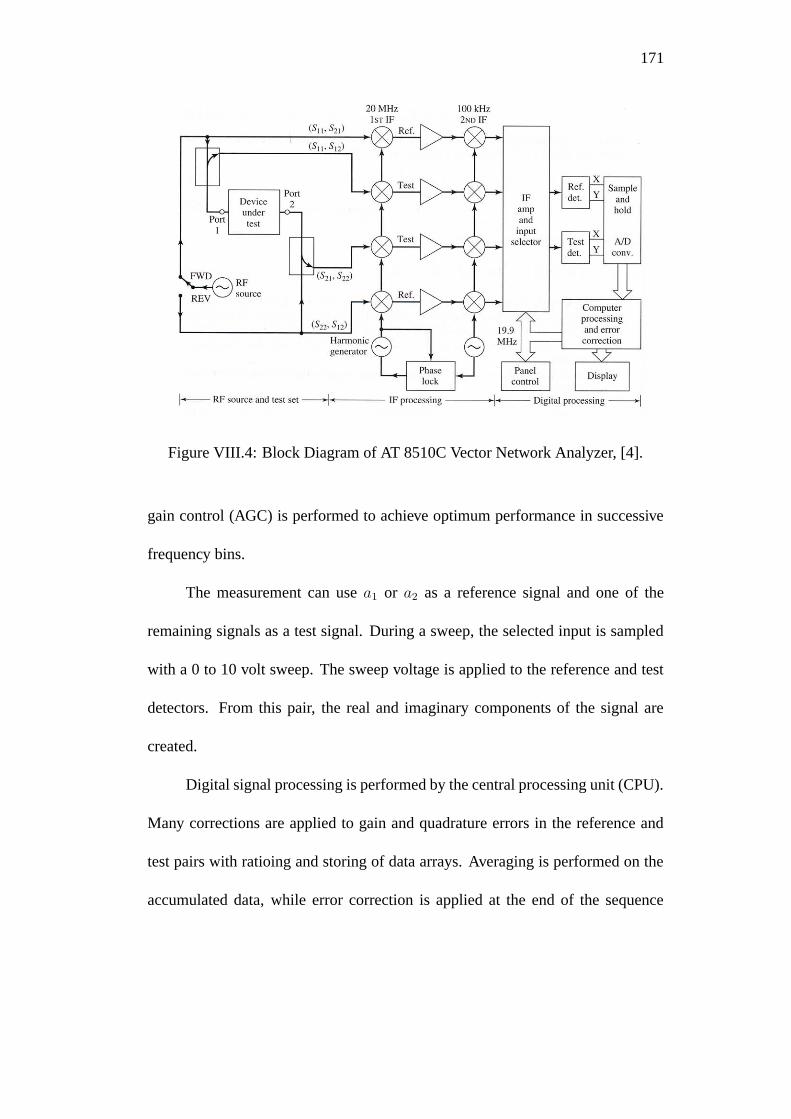
VIII.4 Block Diagram of AT 8510C Vector Network Analyzer, [4]. . . . . 171
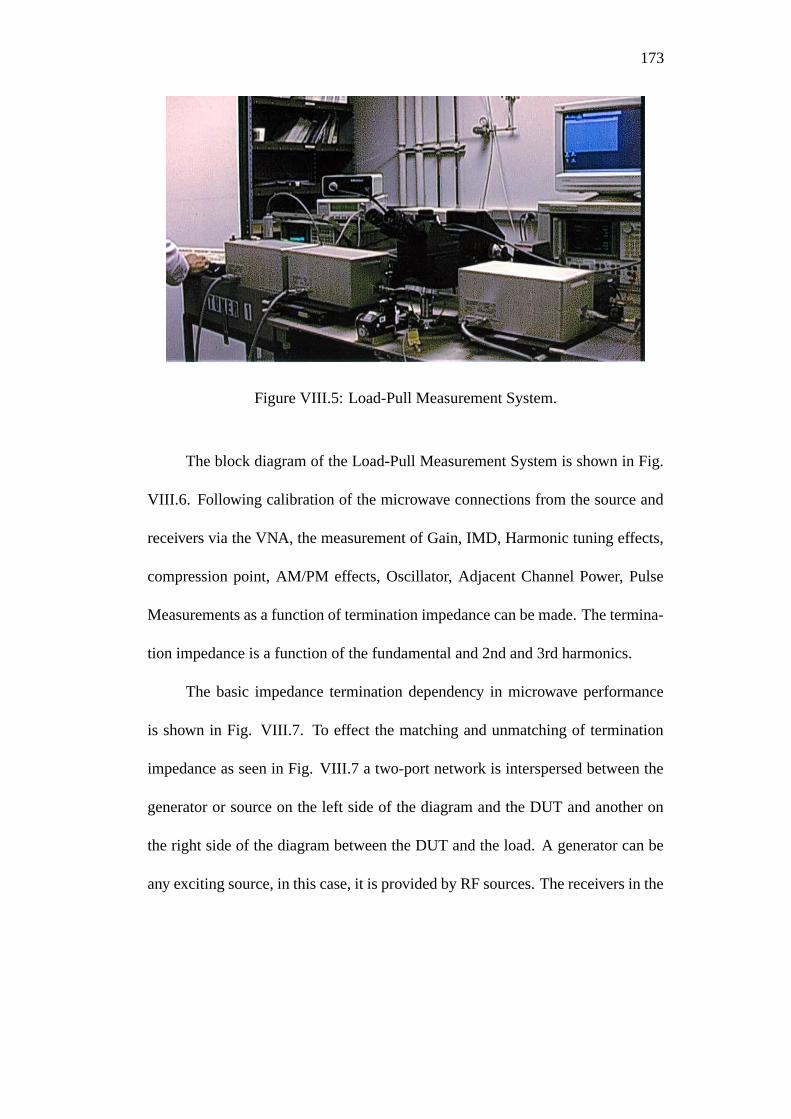
VIII.5 Load-Pull Measurement System. . . . . . . . . . . . . . . . . . . . . . . . . . . . 173
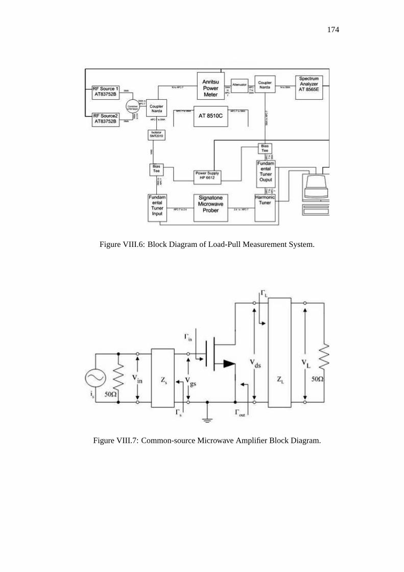
VIII.6 Block Diagram of Load-Pull Measurement System. . . . . . . . . . . . 174
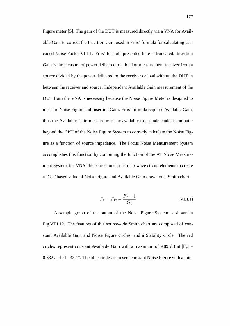
VIII.7 Common-source Microwave Amplifier Block Diagram. . . . . . . . 174
VIII.8 Block Diagram of Noise Measurement System. . . . . . . . . . . . . . . 176
VIII.9 Simplified Noise Measurement Schematic, [5]. . . . . . . . . . . . . . . . 176
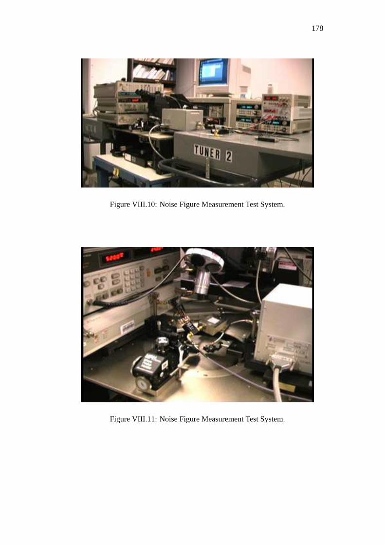
VIII.10 Noise Figure Measurement Test System. . . . . . . . . . . . . . . . . . . . . 178
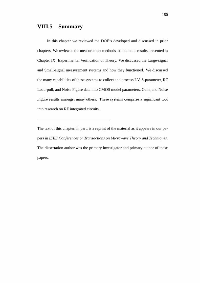
VIII.11 Noise Figure Measurement Test System. . . . . . . . . . . . . . . . . . . . . 178
xi
Page 12
VIII.12 Noise Figure Measurement showing Noise and Available Gain
Circles. . . . . . . . . . . . . . . . . . . . . . . . . . . . . . . . . . . . . . . . . . . . . . . . . 179
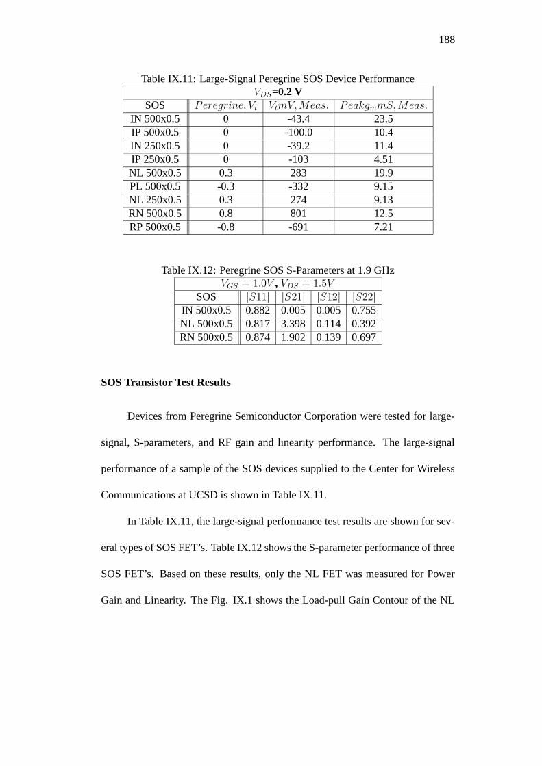
IX.1 SOS Gain Load-pull Contour. . . . . . . . . . . . . . . . . . . . . . . . . . . . . . 189
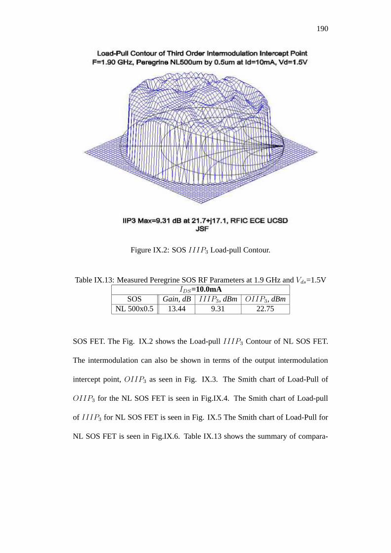
IX.2 SOS IIIP3 Load-pull Contour. . . . . . . . . . . . . . . . . . . . . . . . . . . . . 190
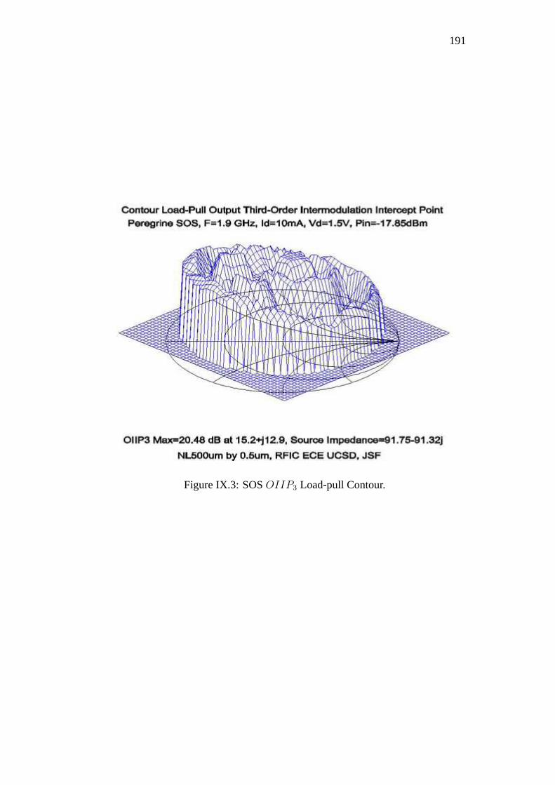
IX.3 SOS OIIP3 Load-pull Contour. . . . . . . . . . . . . . . . . . . . . . . . . . . . 191
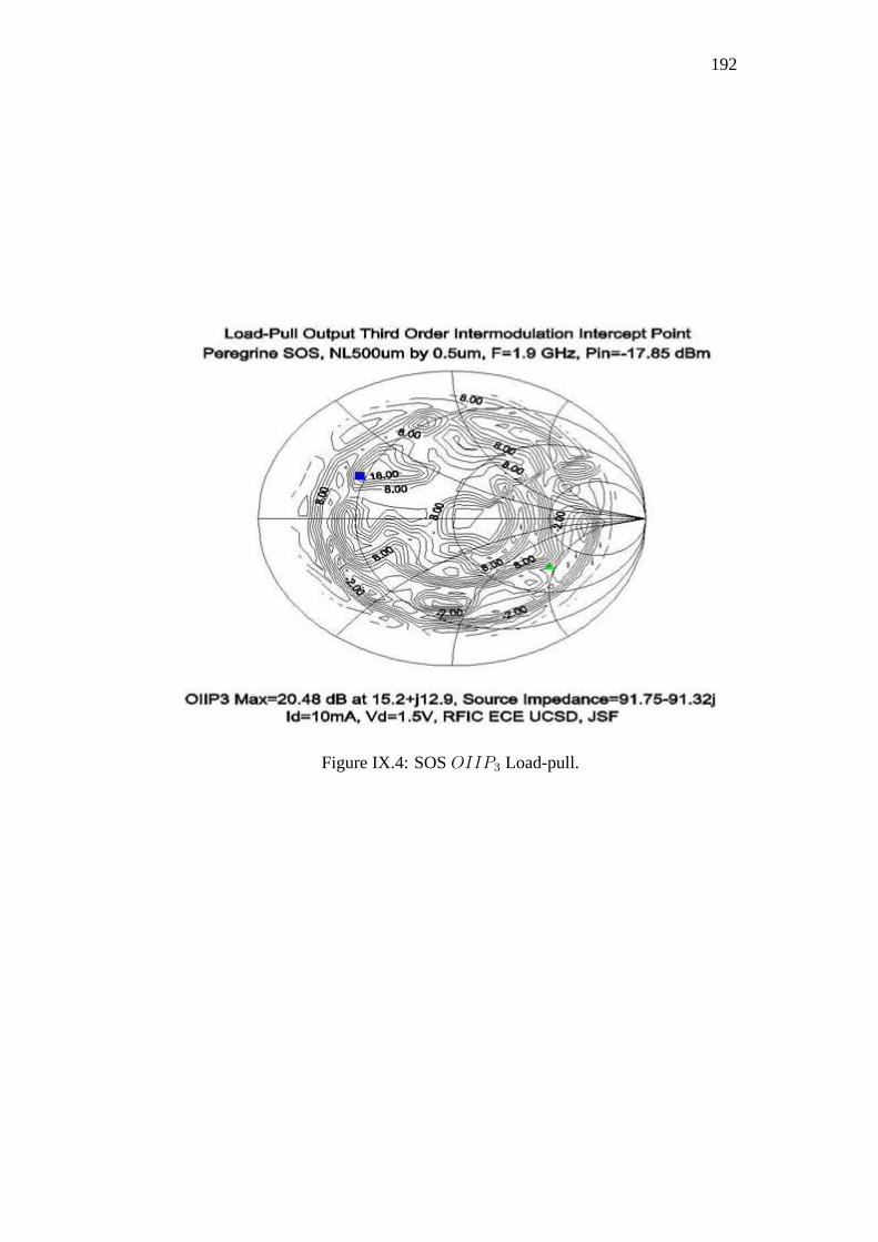
IX.4 SOS OIIP3 Load-pull. . . . . . . . . . . . . . . . . . . . . . . . . . . . . . . . . . . . 192
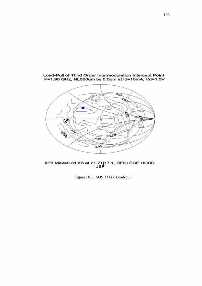
IX.5 SOS IIIP3 Load-pull. . . . . . . . . . . . . . . . . . . . . . . . . . . . . . . . . . . . 193
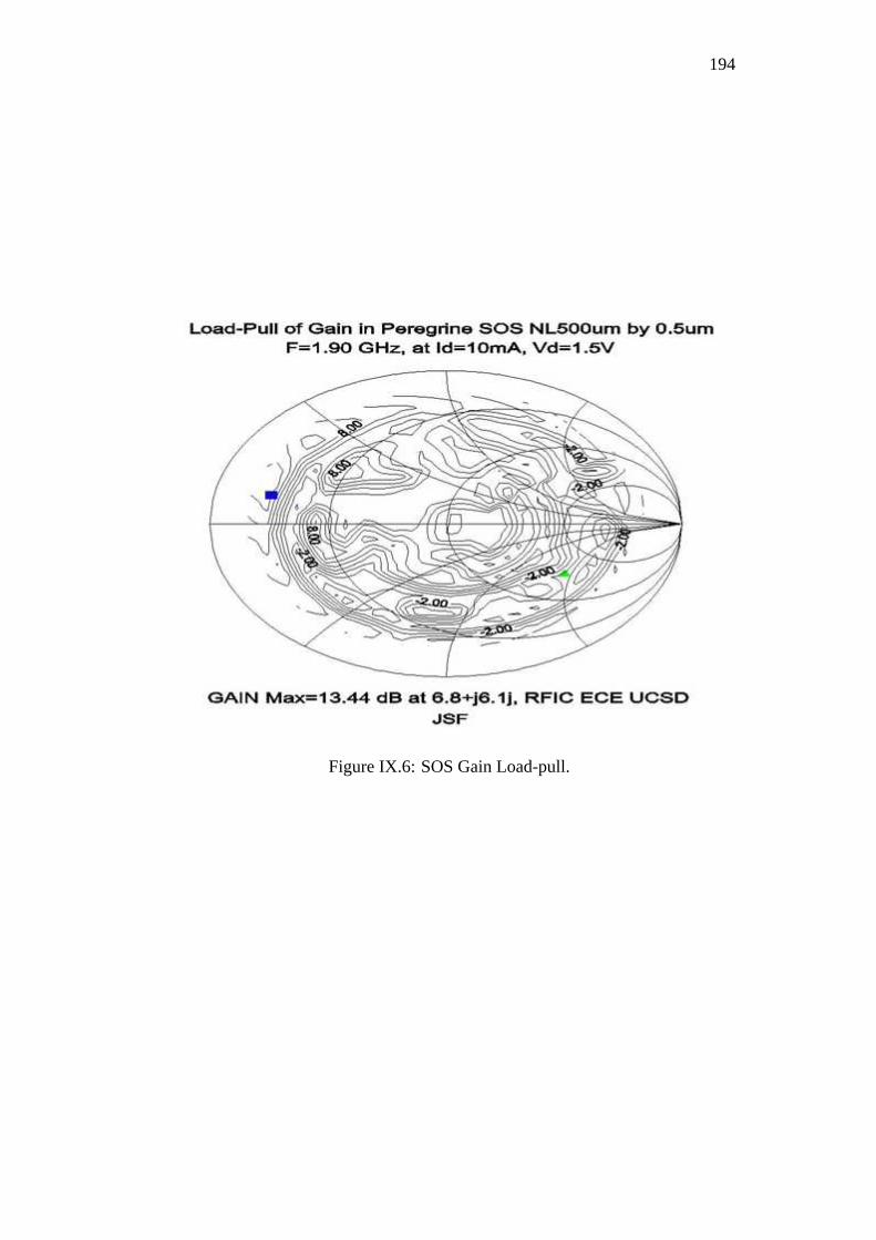
IX.6 SOS Gain Load-pull. . . . . . . . . . . . . . . . . . . . . . . . . . . . . . . . . . . . . 194
IX.7 HBT IIIP3 Load-pull. . . . . . . . . . . . . . . . . . . . . . . . . . . . . . . . . . . . 195
IX.8 HBT Gain Load-pull. . . . . . . . . . . . . . . . . . . . . . . . . . . . . . . . . . . . . 196
IX.9 HBT Gain Load-pull. . . . . . . . . . . . . . . . . . . . . . . . . . . . . . . . . . . . . 197
IX.10 HBT IIIP3 Load-pull Contour. . . . . . . . . . . . . . . . . . . . . . . . . . . . 198
IX.11 HBT IIIP3 Load-pull Contour. . . . . . . . . . . . . . . . . . . . . . . . . . . . 199
IX.12 HBT Gain Load-pull Contour. . . . . . . . . . . . . . . . . . . . . . . . . . . . . . 200
IX.13 HBT Gain Load-pull Contour. . . . . . . . . . . . . . . . . . . . . . . . . . . . . . 201
IX.14 N50µm x 0.35µm Maximum Gain and Maximum IIIP3 vs.
Current Density, Load Side Tuning. . . . . . . . . . . . . . . . . . . . . . . . . 209
IX.15 N50µm x 0.35µm Maximum Gain, IIIP3, Minimum Noise
Figure vs. Current Density, Source Side Tuning. . . . . . . . . . . . . . 210
IX.16 N200µm x 0.35µm Maximum Gain and IIIP3 vs. Current
Density, Load Side . . . . . . . . . . . . . . . . . . . . . . . . . . . . . . . . . . . . . . 211
IX.17 N200µm x 0.35µm Maximum IIIP3, Gain and Minimum Noise
Figure vs. Current Density, Source Side Tuning. . . . . . . . . . . . . . 212
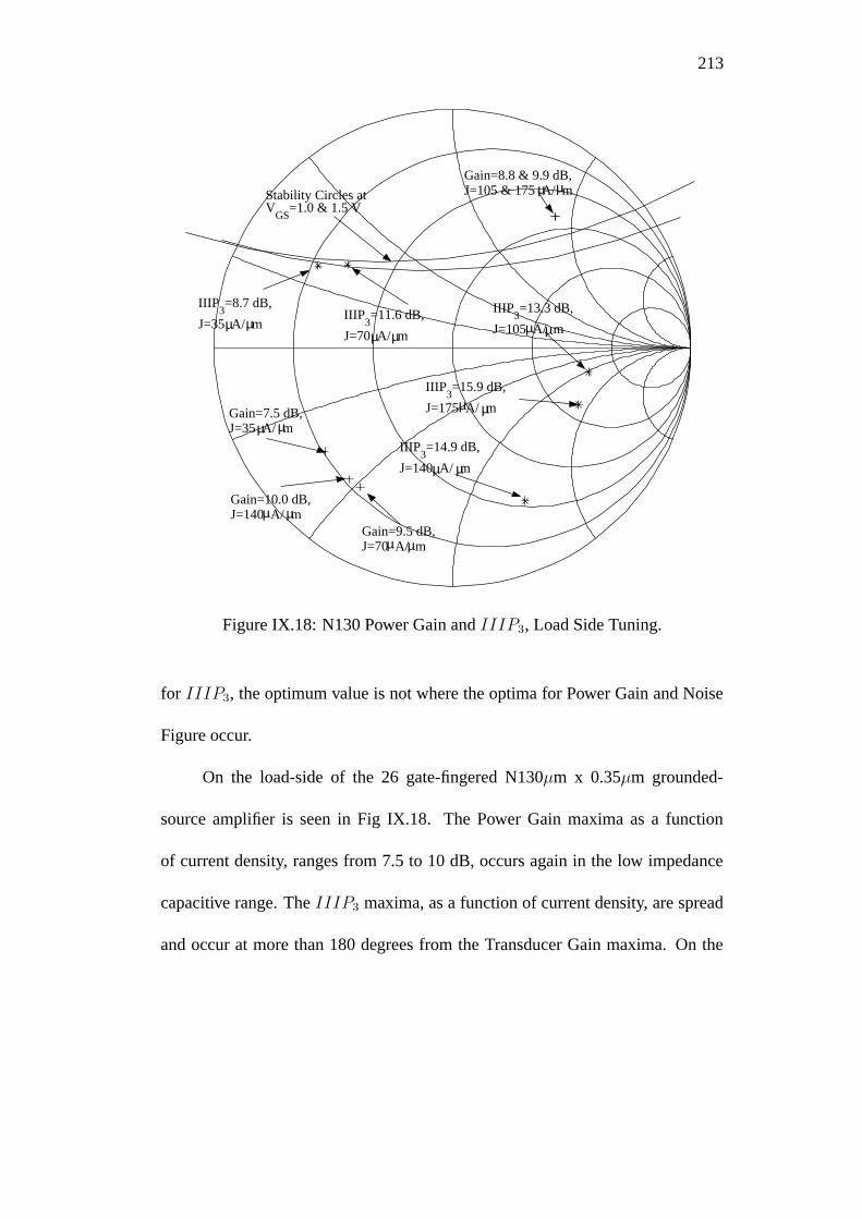
IX.18 N130 Power Gain and IIIP3, Load Side Tuning. . . . . . . . . . . . . . 213
IX.19 N130 Maximum Gain, IIIP3, and Minimum Noise Figure vs.
Current Density, Source Side Tuning. . . . . . . . . . . . . . . . . . . . . . . . 215
IX.20 N520 Maximum Gain and IIIP3 vs. Current Density, Load
Side Tuning. . . . . . . . . . . . . . . . . . . . . . . . . . . . . . . . . . . . . . . . . . . . 216
IX.21 N520 Maximum Gain, IIIP3, and Minimum NF vs. Current
Density, Source Side Tuning. . . . . . . . . . . . . . . . . . . . . . . . . . . . . . . 217
IX.22 5.0 GHz CMOS LNA Test Results . . . . . . . . . . . . . . . . . . . . . . . . . 219
xii
Page 13
LIST OF TABLES
II.1 ISM Radio Receiver Requirements . . . . . . . . . . . . . . . . . . . . . . . . . 19
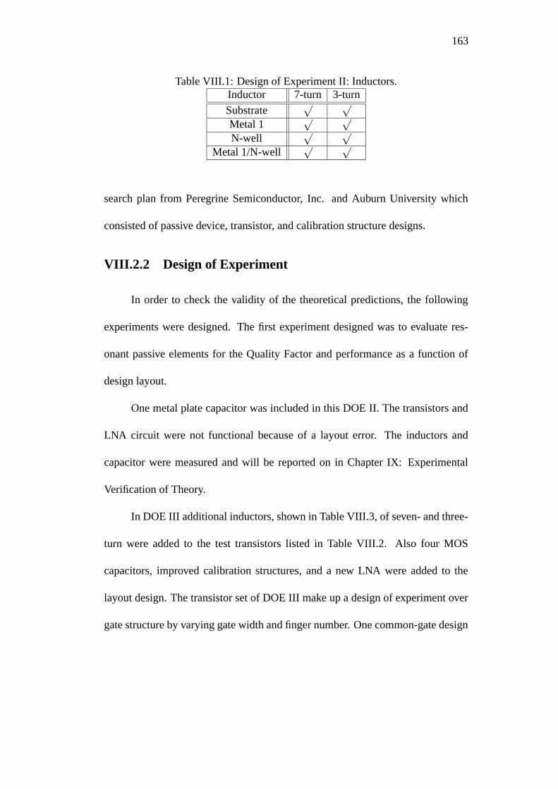
III.1 Large-Signal CMOS Parameters for L=0.35µm at VDS = 1.5V . 30III.2 Transconductance Coefficients for Nonlinear Analysis, gm . . . . . 40III.3 Output Conductance, go . . . . . . . . . . . . . . . . . . . . . . . . . . . . . . . . . . 45III.4 Output Capacitance, cDS . . . . . . . . . . . . . . . . . . . . . . . . . . . . . . . . . 50III.5 Input Capacitance, cGS . . . . . . . . . . . . . . . . . . . . . . . . . . . . . . . . . . . 55III.6 Design of Experiment II: Inductors . . . . . . . . . . . . . . . . . . . . . . . . . 66III.7 Test Transistor Geometry . . . . . . . . . . . . . . . . . . . . . . . . . . . . . . . . . 67III.8 Design of Experiment III: Inductors . . . . . . . . . . . . . . . . . . . . . . . . 67III.9 Test Capacitor Geometry . . . . . . . . . . . . . . . . . . . . . . . . . . . . . . . . . 68III.10 Design of Experiment V: Inductors . . . . . . . . . . . . . . . . . . . . . . . . . 68III.11 Design of Experiment V: Transformers . . . . . . . . . . . . . . . . . . . . . 68
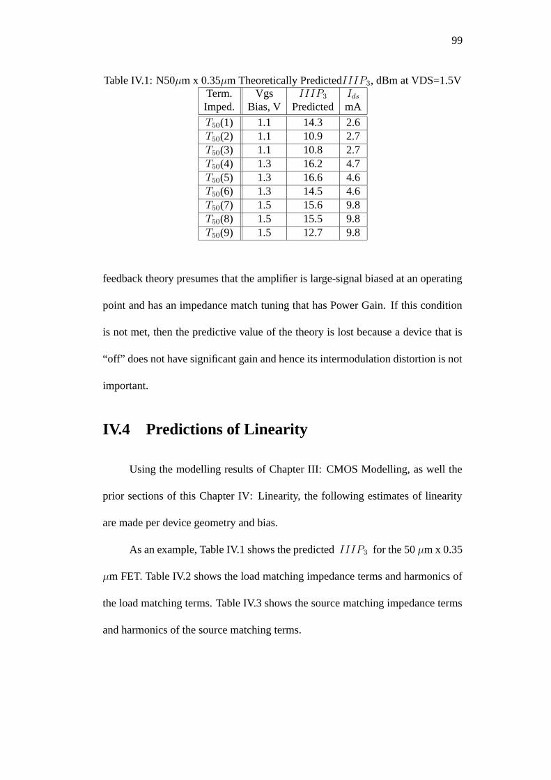
IV.1 N50µm x 0.35µm Theoretically PredictedIIIP3, dBm at VDS=1.5V . . . . . . . . . . . . . . . . . . . . . . . . . . . . . . . . 99
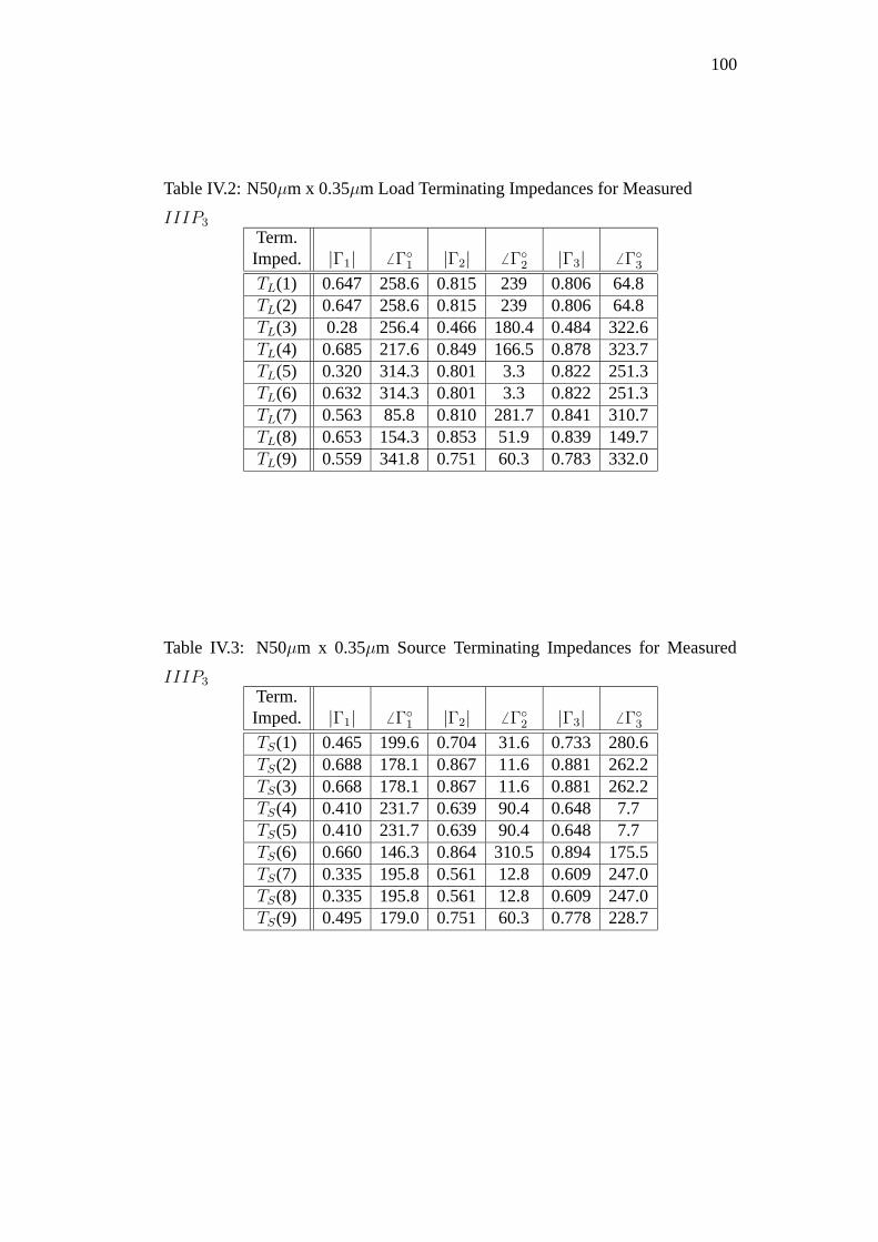
IV.2 N50µm x 0.35µm Load Terminating Impedances for MeasuredIIIP3 . . . . . . . . . . . . . . . . . . . . . . . . . . . . . . . . . . . . . . . . . . . . . . . . 100
IV.3 N50µm x 0.35µm Source Terminating Impedances for Mea-sured IIIP3 . . . . . . . . . . . . . . . . . . . . . . . . . . . . . . . . . . . . . . . . . . . 100
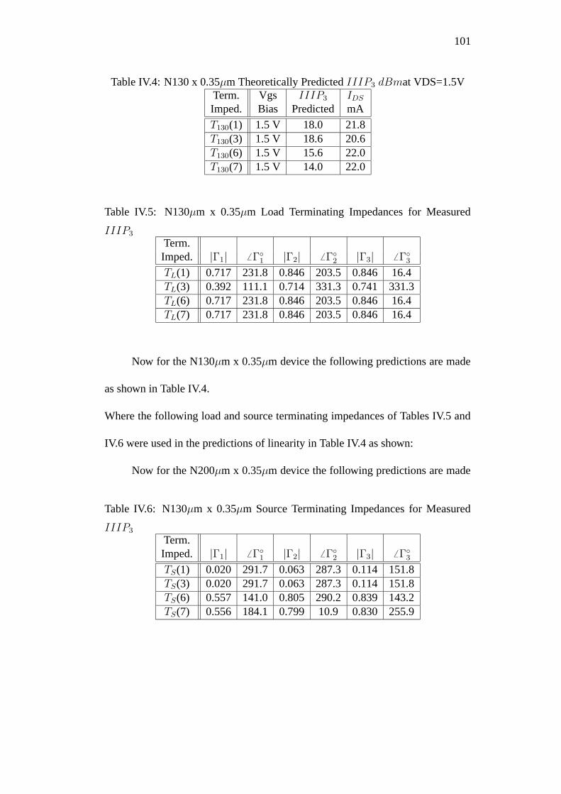
IV.4 N130 x 0.35µm Theoretically Predicted IIIP3 dBmat VDS=1.5V . . . . . . . . . . . . . . . . . . . . . . . . . . . . . . . . . . . . . . . . . . . 101
IV.5 N130µm x 0.35µm Load Terminating Impedances for Mea-sured IIIP3 . . . . . . . . . . . . . . . . . . . . . . . . . . . . . . . . . . . . . . . . . . . 101
IV.6 N130µm x 0.35µm Source Terminating Impedances for Mea-sured IIIP3 . . . . . . . . . . . . . . . . . . . . . . . . . . . . . . . . . . . . . . . . . . . 101
IV.7 N200 x 0.35µm Theoretically Predicted IIIP3 dBmat VDS=1.5V . . . . . . . . . . . . . . . . . . . . . . . . . . . . . . . . . . . . . . . . . . . 102
IV.8 N200µm x 0.35µm Load Terminating Impedances for Mea-sured IIIP3 . . . . . . . . . . . . . . . . . . . . . . . . . . . . . . . . . . . . . . . . . . . 102
IV.9 N200µm x 0.35µm Source Terminating Impedances for Mea-sured IIIP3 . . . . . . . . . . . . . . . . . . . . . . . . . . . . . . . . . . . . . . . . . . . 102
IV.10 Test Transistor Geometry . . . . . . . . . . . . . . . . . . . . . . . . . . . . . . . . . 103
V.1 Noise Theory Predictions at 5 GHz with Γopt and without Feed-back . . . . . . . . . . . . . . . . . . . . . . . . . . . . . . . . . . . . . . . . . . . . . . . . . . 115
V.2 Two-Port Noise Figure Predictions at 5.0 GHz with Γopt andFeedback. . . . . . . . . . . . . . . . . . . . . . . . . . . . . . . . . . . . . . . . . . . . . . . 115
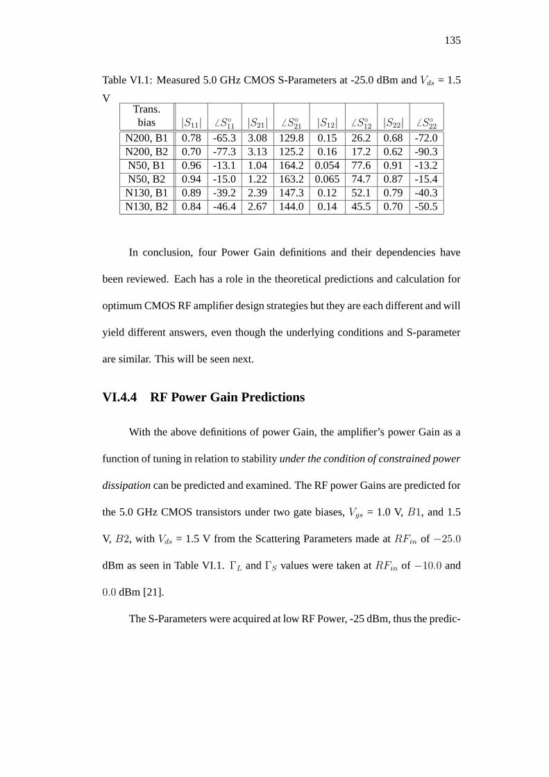
VI.1 Measured 5.0 GHz CMOS S-Parameters at -25.0 dBm and Vds
= 1.5 V . . . . . . . . . . . . . . . . . . . . . . . . . . . . . . . . . . . . . . . . . . . . . . . . 135
xiii
Page 14
VI.2 Calculated Power Gain, dB, at 5.0 GHz based on OptimumLoad-side Matching . . . . . . . . . . . . . . . . . . . . . . . . . . . . . . . . . . . . . 136
VI.3 Calculated Power Gain, dB, at 5.0 GHz based on OptimumSource-side Matching . . . . . . . . . . . . . . . . . . . . . . . . . . . . . . . . . . . . 138
VI.4 SFDR of Si CMOS Grounded-Source Amplifiers, Source Side,VDS=VGS=1.5V . . . . . . . . . . . . . . . . . . . . . . . . . . . . . . . . . . . . . . . . . 143
VII.1 IMS LNA 5.0 GHz Design Goals . . . . . . . . . . . . . . . . . . . . . . . . . . 150VII.2 Design Specifications of 26.0 GHz CMOS LNA . . . . . . . . . . . . . . 156
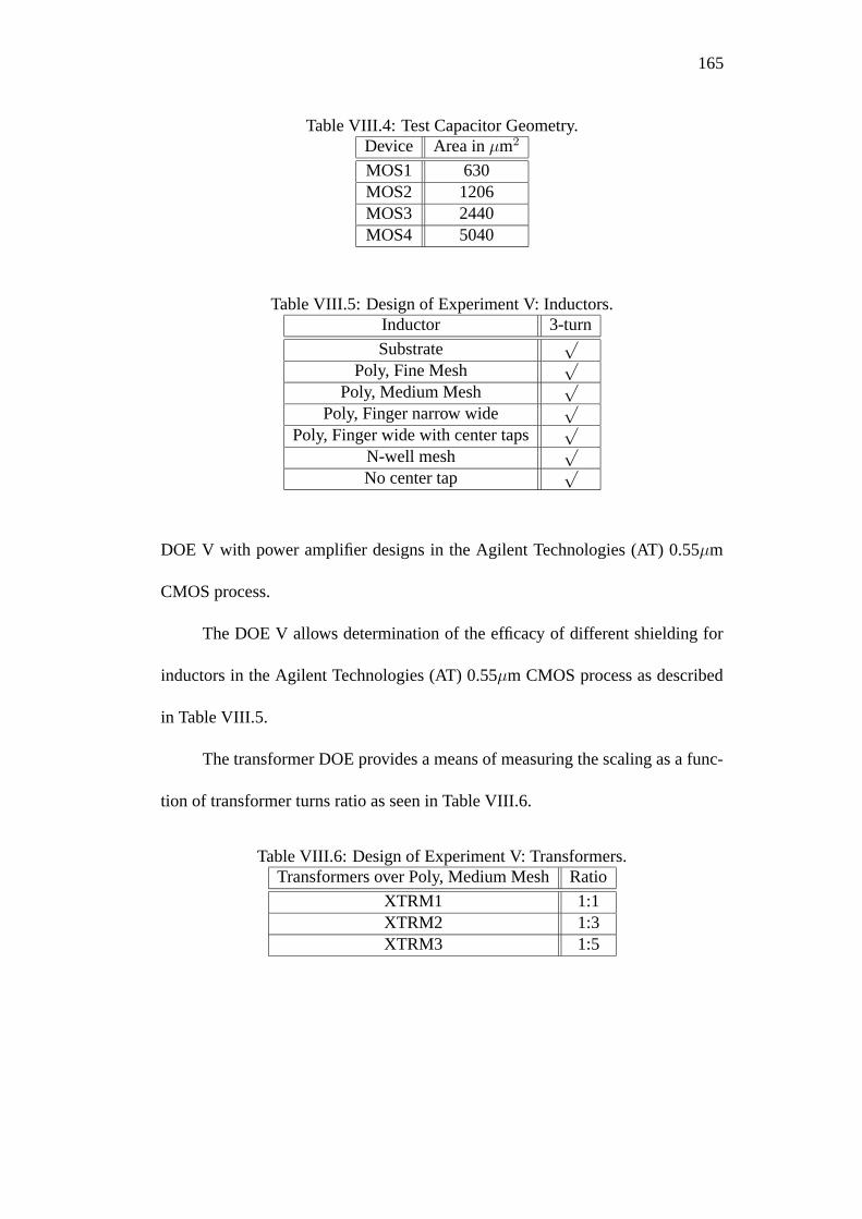
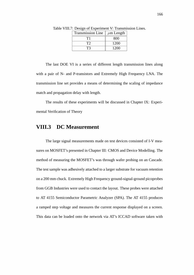
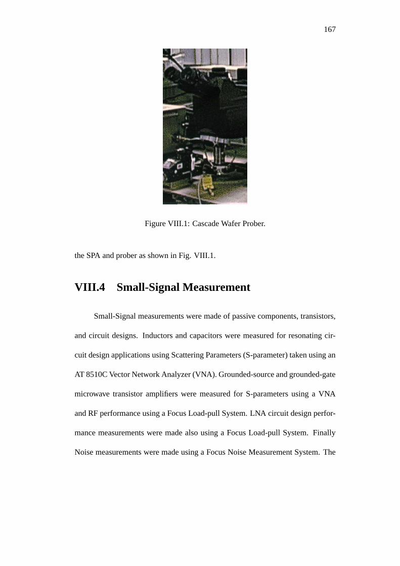
VIII.1 Design of Experiment II: Inductors. . . . . . . . . . . . . . . . . . . . . . . . . 163VIII.2 Test Transistor Geometry. . . . . . . . . . . . . . . . . . . . . . . . . . . . . . . . . 164VIII.3 Design of Experiment III: Inductors. . . . . . . . . . . . . . . . . . . . . . . . 164VIII.4 Test Capacitor Geometry. . . . . . . . . . . . . . . . . . . . . . . . . . . . . . . . . . 165VIII.5 Design of Experiment V: Inductors. . . . . . . . . . . . . . . . . . . . . . . . . 165VIII.6 Design of Experiment V: Transformers. . . . . . . . . . . . . . . . . . . . . . 165VIII.7 Design of Experiment V: Transmission Lines. . . . . . . . . . . . . . . . . 166
IX.1 Measured CMOS N-channel devices of L=0.35µm Large-SignalLinear Parameters at VDS=1.5V . . . . . . . . . . . . . . . . . . . . . . . . . . . 182
IX.2 CMOS N-channel devices of L=0.35µm Large-Signal Satura-tion Parameters at VDS=1.5V . . . . . . . . . . . . . . . . . . . . . . . . . . . . . 183
IX.3 Measured 5.0 GHz CMOS Scattering Parameters at -25.0 dBm . 183IX.4 Extracted gm polynomial coefficients fit to measured data at
VDS and VGS=1.5V . . . . . . . . . . . . . . . . . . . . . . . . . . . . . . . . . . . . . . 184IX.5 Transconductance, gm Differences Measured v. Modelled . . . . . . 185IX.6 Extracted Polynomial Output Conductance, go, Fit to Measured
Data at VDS=1.5V, VGS=1.0V . . . . . . . . . . . . . . . . . . . . . . . . . . . . . 185IX.7 Output Capacitance, cDS . . . . . . . . . . . . . . . . . . . . . . . . . . . . . . . . . 186IX.8 Output Capacitance, CDS Differences Measured v. Modelled . . . 186IX.9 Input Capacitance, cGS . . . . . . . . . . . . . . . . . . . . . . . . . . . . . . . . . . . 187IX.10 Input Capacitance, CGS Differences Measured v. Modelled . . . . 187IX.11 Large-Signal Peregrine SOS Device Performance . . . . . . . . . . . . 188IX.12 Peregrine SOS S-Parameters at 1.9 GHz . . . . . . . . . . . . . . . . . . . . 188IX.13 Measured Peregrine SOS RF Parameters at 1.9 GHz and Vds=1.5V190IX.14 RF Parameters of IBM HBT’s at 1.9 GHz. . . . . . . . . . . . . . . . . . . . 196IX.15 Design of Experiment II Results: Inductor Performance . . . . . . . 202IX.16 Design of Experiment III Results: Inductor Performance . . . . . . 202IX.17 N50µmx0.35µm Predicted vs. Measured IIIP3, dBm
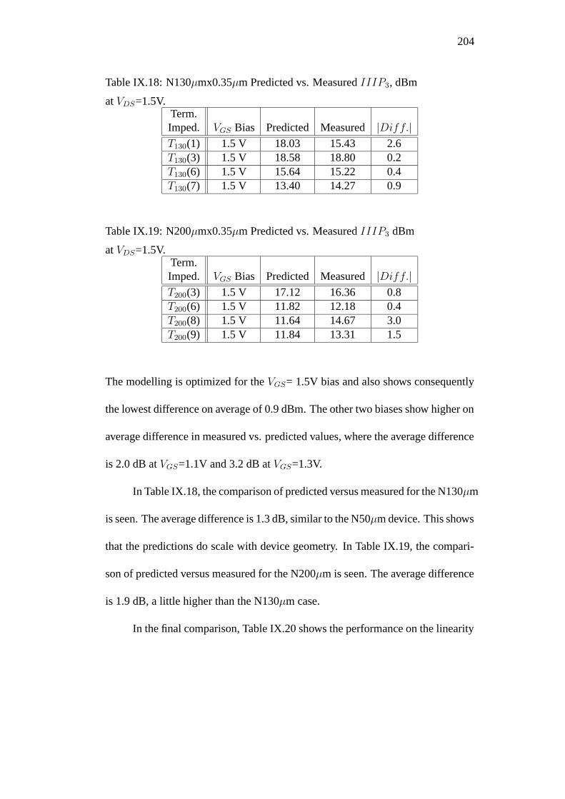
at VDS=1.5V . . . . . . . . . . . . . . . . . . . . . . . . . . . . . . . . . . . . . . . . . . . 203IX.18 N130µmx0.35µm Predicted vs. Measured IIIP3, dBm
at VDS=1.5V. . . . . . . . . . . . . . . . . . . . . . . . . . . . . . . . . . . . . . . . . . . . 204
xiv
Page 15
IX.19 N200µmx0.35µm Predicted vs. Measured IIIP3 dBmat VDS=1.5V. . . . . . . . . . . . . . . . . . . . . . . . . . . . . . . . . . . . . . . . . . . . 204
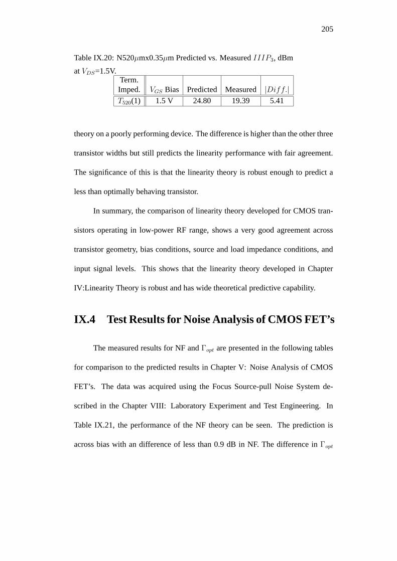
IX.20 N520µmx0.35µm Predicted vs. Measured IIIP3, dBmat VDS=1.5V. . . . . . . . . . . . . . . . . . . . . . . . . . . . . . . . . . . . . . . . . . . . 205
IX.21 N50µm Two-Port NF Prediction vs. Measured at VDS=1.5 V . . . 206IX.22 N130µm Two-Port NF Prediction vs. Measured at VDS=1.5 V . . 206IX.23 N200µm Two-Port NF Prediction vs. Measured at VDS=1.5V . . 206IX.24 ISM LNA 5.0 GHz Design . . . . . . . . . . . . . . . . . . . . . . . . . . . . . . . . 220IX.25 5.0 GHz CMOS LNA Performance Comparison . . . . . . . . . . . . . . 221
xv
Page 16
ACKNOWLEDGEMENTS
It is my great pleasure to take this opportunity to thank everyone who made
this dissertation possible.
First and foremost, I would like to express my sincere gratitude and appreci-
ation to my advisor Professor Lawrence E. Larson and Professor Peter M. Asbeck
for their unfailing and invaluable guidance and support. I have especially ben-
efited from their constructive comments and invaluable suggestions throughout
this project. I would like to thank also the members of my committee, Professor
Paul K. Yu , Professor Robert Bitmead and Professor Michael J. Sailor, for their
suggestions and recommendations.
Special thanks to my brilliant colleagues for their enthusiastic help and en-
couragement. I would like to acknowledge some amongst many who contributed:
Ed Chen, Jonathan Jensen, Liwei Sheng, Chengzhou Wang, and Matt Wetzel.
This research was supported by the US Army Research Office Muri-University
Research Initiative Program Digital Communication Devices Based on Nonlinear
Dynamics and Chaos, and the UCSD Center for Wireless Communications and its
member companies. The California State Micro Program. Their support is greatly
appreciated.
The text of Chapters III, IV, V, VI, VII, VIII, and IX in this dissertation, in
part or in full, is a reprint of the material as it appears in our published papers or
as it has been submitted for publication in IEEE Journal of Solid State Circuits,
xvi
Page 17
IEEE Transactions on Microwave Theory and Techniques, and IEEE Transactions
on Electron Devices. The dissertation author was the primary author listed in these
publications directed and supervised the research which forms the basis for these
chapters.
xvii
Page 18
VITA
1982 B.A., Physics and Mathematics (Applied), Univer-sity of California, San Diego
1982-1984 Product Engineer, Burroughs Corporation, San Diego,California
1984-1985 Design Engineer, TRW LSI Products Division, LaJolla, California
1986-1991 Staff Engineer, Hughes Aircraft Corporation, Carls-bad, California
1990 M.S., Physics, San Diego State University, San Diego,California
1991-1992 Principal Engineer, Silicon Systems, Incorporated,Tustin, California
1992-present President, Fairbanks Laboratories, San Diego, Cal-ifornia
1992-1993 Adjunct Faculty, Southwestern and Palomar Col-leges, San Diego County, California
1993-1996 Product/Design Engineer, Pacific CommunicationSciences, Incorporated, San Diego, California
2001 P.E., Electrical Engineering, E 16362, CaliforniaState Board
1997-2003 Research Assistant, University of California, SanDiego
2002 C.Phil., Electrical and Computer Engineering, Uni-versity of California, San Diego
2003 Ph.D., Electrical and Computer Engineering (Elec-tronic Circuits & Systems), University of Califor-nia, San Diego
xviii
Page 19
PUBLICATIONS
John S. Fairbanks, Larry E. Larson, “A 5 GHz Low-Power, High-Linearity Low-Noise Amplifier in a Digital 0.35µm CMOS Process”, IEEE MTTS Radio andWireless Conference, 2003
John S. Fairbanks, Larry E. Larson, “Analysis of Optimized Input and OutputHarmonic Termination on the Linearity of 5 GHz CMOS Radio Frequency Am-plifiers”, IEEE MTTS Radio and Wireless Conference, 2003
John S. Fairbanks, Larry E. Larson, “Analysis of Termination Impedance Effectson the Linearity of 5 GHz Radio Frequency Amplifiers”, Si RF Workshop, IEEEMicrowave Theory and Techniques, Germany, April 2003
Guofu Niu, Shiming Zhang, John D. Cressler, Alvin J. Joseph, John S. Fairbanks,Larry E. Larson, Charles E. Webster, William E. Ansley, and David L. Harame,“Noise Modeling and SiGe Profile Design Tradeoffs for RF Applications”, IEEETransactions on Electron Devices, vol. 47, p.2037, November 2000
Guofu Niu, Shiming Zhang, John D. Cressler, Alvin J. Joseph, John S. Fairbanks,Larry E. Larson, Charles E. Webster, William E. Ansley, and David L. Harame,“Noise Parameter Modeling and SiGe Profile Design Tradeoffs for RF Circuit Ap-plications”, Si RF Workshop, IEEE Microwave Theory and Techniques, Germany,April 2000 [Invited Paper]
Guofu Niu, Shiming Zhang, John D. Cressler, Alvin J. Joseph, John S. Fairbanks,Larry E. Larson, Charles E. Webster, William E. Ansley, and David L. Harame,“SiGe Profile Design Tradeoffs for RF Circuit Applications”, Solid-State Devices,IEEE International Electron Devices Meeting, December 1999
John S. Fairbanks, “A Comparison Between Deterministic and Pseudo-RandomTests”, Test Technology Newsletter, IEEE Computer Society, October 1984.
FIELDS OF STUDY
Major Field: Electrical and Computer Engineering (Electronic Circuits and Systems)
Studies in Radio Frequency Integrated Circuit Design.Professor Lawrence E. Larson
xix
Page 20
ABSTRACT OF THE DISSERTATION
5 GHz CMOS LNA/Receiver Design for Wireless Local Area Networks
by
John S. Fairbanks
Doctor of Philosophy in Electrical and Computer Engineering
(Electronic Circuits & Systems)
University of California, San Diego, 2003
Professor Lawrence E. Larson, Chair
Portable, wireless, personal-communication devices continue to gain in pop-
ularity, and CMOS technology is becoming increasingly popular for the realiza-
tion of key radio frequency components [6–8]. Although the intrinsic speed of
scaled MOS devices is impressive, the use of CMOS devices for high-frequency
applications has been limited by the “digital” orientation of the design and mod-
elling environment. In particular, the optimum scaling, biasing, and tuning of the
devices for the realization of the best high-frequency performance in a wireless
environmental remains a challenge [9].
The purpose of this work is to develop some straightforward guidelines for
simultaneously optimizing the linearity, noise, and dynamic range of the mono-
lithic common-source MOS amplifier in an RF LNA, variable gain amplifier (VGA),
xx
Page 21
and mixer applications in a wireless transceiver, under the constraint of minimiz-
ing dc power dissipation. In a sense, this extends the earlier work of Schaefer
and Lee [6] on power-constrained MOS LNA design to include linearity consid-
erations. The experimental results presented verify the utility of this technique,
and point the way towards fully monolithic CMOS transceivers with improved
power/noise/linearity tradeoffs.
Following a brief introduction to RF systems and radio architecture, a de-
tailed analysis of the device modelling, both active and passive, followed by pre-
diction in performance from theory is made. Next, the theory of high-frequency
linearity is developed to include nonlinear device behavior, impedance termina-
tion matching at the fundamental, second, and third harmonic, and feedback, fol-
lowed by predictions. Next, noise modelling of MOS devices with feedback is
developed and then the noise performance of the common-source amplifier is pre-
dicted. Next, an analysis of power-constrained dynamic range limitations on the
MOS common-source amplifier and its implications on system performance re-
quirements is discussed, concluding with predictions on tradeoffs.
Next, the theoretical techniques developed above are applied to the design of
a 5 GHz low-power, high-linearity low-noise amplifier in a digital 0.35µm CMOS
process. The circuit is simulated, fabricated, and tested.
A discussion detailing the test engineering necessary to verify all of the
above results is provided. After which results from each area, device modelling,
xxi
Page 22
linearity, noise theory, RF optimization techniques, and circuit design are re-
viewed and compared to theoretical predictions.
xxii
Page 23
Chapter I
Introduction and System
Architecture
I.1 Introduction to System Architecture
The purpose of this chapter is to discuss the system level requirements for
establishing goals in circuit design and device performance. Without review-
ing and assessing these requirements, the context for the lower level achieve-
ments becomes less relevant. So, the background of system analysis relevant to
high frequency circuit design and device performance is reviewed using Orthog-
onal Frequency Division Multiplexing (OFDM) as an example system architec-
ture. OFDM is a system architecture applicable to Wireless Local Area Networks
(WLAN) [10].
1
Page 24
2
Format Modulate
Format Demodulate
X M T
R C V
Information Source
Information Sink
Channel
Figure I.1: RF System Block Diagram
I.2 System Architecture Overview
System architecture is the means by which the information, such as a per-
son talking, is conveyed some distance through a medium and reconstructed for
a signal receiver, such as a person listening. A Radio provides a means for this
communication through the atmosphere and space. Fig. I.1 shows a simple com-
munication system as a guide for further discussion [11].
I.3 Information Modulation in an RF System
Source formatting is the process by which an analog signal is converted to
a discrete signal for digital communication systems. This process is in part done
through an Analog-to-Digital converter (ADC). The reverse is achieved through a
digital-to-analog converter (DAC) when processing a signal through a receiver.
Modulation is a process by which information signals impressed on a car-
Page 25
3
rier, which can be transmitted across a medium; that is, where A(t) and Θ(t)
contain the information.
S(t) = A(t) cos(ωct+ θ(t)) (I.1)
Demodulation that uses the phase of the carrier is called coherent detection,
and demodulation which does not use knowledge about the phase of the carrier is
non-coherent detection [10].
Three common methods exist for using a fixed communication channel:
Frequency Division Multiple Access (FDMA), Time Division Multiple Access
(TDMA), and Code Division Multiple Access (CDMA). Briefly, the FDMA mod-
ulation scheme uses non-overlapping frequency bands. TDMA uses non-overlapping
time slots. CDMA uses orthogonal coding to gain use of the entire time-frequency
space. There are distinct advantages and disadvantages to each method, which will
not be reviewed here but some references in the bibliography at the end of this dis-
sertation can provide more background information. A consequence however of
the choice of a scheme for using a fixed communication channel is that different
methods will have different outcomes regarding a receiver’s ability to detect cor-
rectly an information signal with a certain quality level. This fact has a bearing on
the system, circuit, and device performance requirements.
Page 26
4
I.4 RF Channel Impairments
The channel referred to in Fig. I.1 is a medium through which the formatted
and modulated signal propagates. The channel is subject to certain losses: Point-
ing loss, antennae are not aligned; Polarization loss from the EM field misalign-
ment of the antennae; Atmospheric loss from water vapor and oxygen absorption
as well as noise sources; Space loss from distance between antennae. These losses
affect the overall communication system performance and affect the requirements
on the circuit and device performance.
Finally a channel can have multi-path fading from the interaction of EM
waves with objects in the path. Multi-path fading is important because it causes
the channel to have time-varying propagation delays, attenuation factors, and
Doppler shifts. Depending on instantaneous details about the channel it can ap-
pear to have flat, Rayleigh, or Rician fading [12].
I.5 RF Receiver
OFDM is a communication scheme designed to counter multi-path fading
with wireless digital communication. It is a hybrid of multiple carriers, instead of
one described in Section I.3 where each carrier can be amplitude and phase modu-
lated, and Frequency Shift Keying (FSK). FSK is a signalling scheme, which can
be detected either coherently or non-coherently, [11], and is described analytically
by
Page 27
5
Si(t) =
√
2E
Tcos(ωit+ φ) (I.2)
and i = 1, 2, 3, ...,M and 0 ≤ t ≤ T .
FSK allows a data set to be orthogonally transmitted per symbol. Combin-
ing OFDM with FSK allows an additional orthogonality for the information which
helps reduce the inter-symbol interference (ISI) caused by multi-path, modelled
by Rayleigh fading. Rayleigh fading is defined by
p(z1|s2) =
z1
σ20
exp(− z21
2σ20
)
(I.3)
when z1 ≥ 0 and 0 otherwise. σ0 represents the noise at the output of the
detection, where z1 is the output of the envelope detector in a non coherent FSK
receiver.
Since the success in receiving a signal is probabilistic in nature, a probability
density function describes the performance. For non-coherent FSK, the definition
of the probability of a bit error is given by
PB = 0.5 exp(−1
2
Eb
No
) (I.4)
where Eb is the energy per bit andNo is the single-side receiver noise power
spectral density ≈ 10−11 W/Hz relative to a 1 Ω load, [11].
Since the successful reception of information is probabilistic, a curve exists
showing the relationship between the Eb/No and the bit error probability, Fig.I.2.
Page 28
6
P e
E b /N o
Figure I.2: Bit Error Probability vs. Eb/No
A relationship exists between the signal to noise ratio, modulation effi-
ciency, and energy/bit, noise power spectral, and the probability of bit error which
can be expressed as
Eb
No
=ST
No
=S
RNo
=SW
RNoW=S
N
(W
R
)
(I.5)
where S is the received power, T is the bit duration time, R = 1/T , N = NoW ,
and W is the bandwidth. What this implies is that the quality factor of the digital
communication figure of merit is proportional to the signal to noise ratio.
I.6 System to Receiver Circuit Design Requirements
The probability of bit error can be determined from the Eb/No because of
the relationship seen in Fig. I.2. With the Eb/No set, which is about 15 dB for
Page 29
7
non-coherent FSK detection, [11], performance requirements can be inferred to
set gain, noise figure, linearity in a radio circuit design. Linearity determines
strongly how much in-band distortion from intermodulation distortion and cross-
modulation distortion will contribute to the error in detection. A more complicated
demodulation receiver could use coherent detection on BPSK, QPSK, or QAM
signals, however increased complexity is required and usually more current will
be consumed. The benefit is that the receiver can usually perform better with a
lower signal-to-noise ratio.
Next, a brief description of QAM and MPSK signalling will be discussed
because, these digital modulation methods often appear in 802.11 receivers which
are employed in WLAN.
Quadrature Amplitude Modulation (QAM) is a modulation scheme which
changes the amplitude and phase of a carrier. Frequency modulation of a carrier is
not allowed in OFDM because it would destroy the orthogonality of the subcarri-
ers which offer the improvements in dealing with channel fading, amongst others.
QAM has a signal constellation which is not restricted to a circle. (A signalling
constellation is an N-dimensional plot of the possible vectors corresponding to the
possible digital signals, [13].)
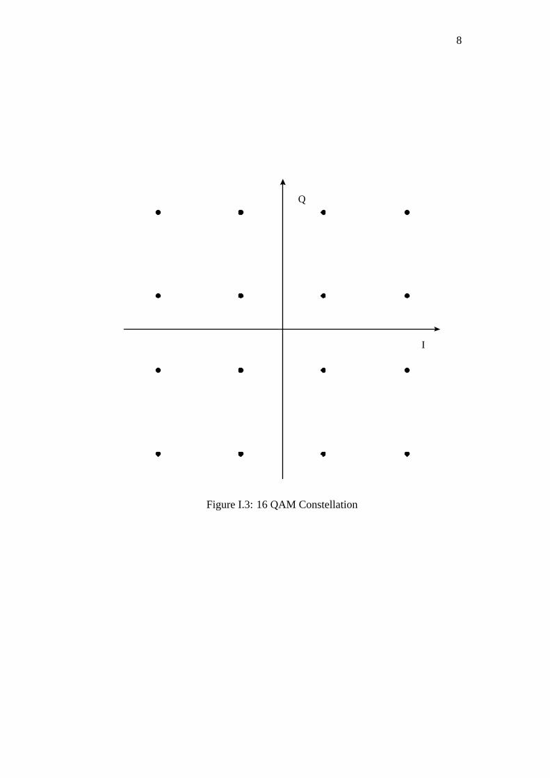
In Fig. I.3 is shown the constellation for sixteen symbol QAM. This sig-
nalling can be generated with two 2-bit DAC’s and has four levels per dimension.
The symbol error rate for QAM can be approximated as shown in (I.6).
Page 30
8
I
Q
Figure I.3: 16 QAM Constellation
Page 31
9
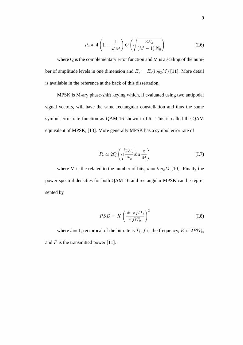
Pe ≈ 4
(
1 − 1√M
)
Q
(√
3Es
(M − 1)N0
)
(I.6)
where Q is the complementary error function and M is a scaling of the num-
ber of amplitude levels in one dimension and Es = Eb(log2M) [11]. More detail
is available in the reference at the back of this dissertation.
MPSK is M-ary phase-shift keying which, if evaluated using two antipodal
signal vectors, will have the same rectangular constellation and thus the same
symbol error rate function as QAM-16 shown in I.6. This is called the QAM
equivalent of MPSK, [13]. More generally MPSK has a symbol error rate of
Pe ' 2Q
(√
2Es
No
sinπ
M
)
(I.7)
where M is the related to the number of bits, k = log2M [10]. Finally the
power spectral densities for both QAM-16 and rectangular MPSK can be repre-
sented by
PSD = K
(
sinπflTb
πflTb
)2
(I.8)
where l = 1, reciprocal of the bit rate is Tb, f is the frequency, K is 2PlTb,
and P is the transmitted power [11].
Page 32
10
I.7 System Architecture Summary
The RF system architecture has been reviewed regarding formatting and
modulation and the effects of channel losses. The use of OFDM to compensate
for multipath losses was introduced. The probability of bit error as a figure of
merit for receiver design was developed in connection with signal-to-noise ratio.
From this signal-to-noise ratio, a radio design requirement may be set. The design
requirements for an ISM radio will be discussed in the next chapter.
I.8 Dissertation Focus
This dissertation will focus on a series of theoretical and experimental areas
that are necessary to predict several relevant device and circuit performances in
Power Gain, linearity, Noise Figure (NF) for 5 GHz amplifier applications. These
areas will lead to higher level suggestions on optimizing circuit performance with
respect to system goals and device capabilities. Thus, after a start with the initial
background in radio architecture and systems, device modelling of CMOS tran-
sistors from a standard digital process is reviewed. From the device modelling,
some characteristics are developed for nonlinear analysis and noise modelling.
Following this theoretical development is a higher level discussion of a figure-
of-merit (FOM), known as Spur-Free Dynamic Range (SFDR) and its relation to
system performance and impedance matching effects on Power Gain, Linearity,
and Noise. Following the recommendations developed from the SFDR discus-
Page 33
11
sions, the theory is applied to LNA circuit design. All of the results from each
of these developments are reviewed in comparison to theoretically predicted val-
ues. Also some time is spent on the test engineering developed to measure each
of these different types of results. The results of a few other technologies are also
reviewed.
In summary, the dissertation shows Volterra analysis linearity prediction
with four small-signal non-linearities in CMOS FET’s based on careful device
modelling and including feedback. Also, a thorough development and predic-
tion of NF for high-frequency device and circuit applications predicting NF as a
function of geometry and bias as well as Γopt, including feedback is presented.
The effect of impedance matching on the above, plus the use of SFDR in circuit
optimization, is shown, followed by an application of the above techniques to
Low-Noise Amplifier (LNA) circuit design.
I.9 Dissertation Organization
The dissertation consists of Ten chapters:
Chapter I:Introduction and System Architecture discusses the background
of system architecture and the design goals that are derived from radio design,
and concludes with this summary of the organization of this dissertation.
Chapter II: Radio Architecture deals with an ISM receiver design to ex-
amine the required performance of Power Gain, Noise Figure, and linearity. The
Page 34
12
estimates of the Power Gain will be made with simple design models and reported
results. Based upon these estimates, an ISM receiver design using a digital CMOS
process will be introduced and studied.
Chapter III:Device Modelling deals with the complex mathematical and
computer modelling of both devices and transistors in preparation for theoretical
RF predictions and design work presented in later chapters. The use of large-
signal data for deriving basic CMOS transistor modelling will be made. The
use of small-signal data from S-parameters will be defined for later predictions
of RF CMOS transistor performance. The use of small-signal data for deriving
nonlinear polynomial expansions will be shown and will be employed to predict
linearity in Chapter IV:Linearity Analysis of MOSFET’s and noise in Chapter V:
Noise Analysis of CMOS FET’s. The construction of transistor models for com-
puter simulation based on physical processes will be described and reviewed. The
use of Finite Element Matrix methods to predict inductance will be reviewed, in
addition to geometrical process based methods.
Chapter IV IV: Linearity Analysis of MOSFET’s deals with the nonlinear
performance of a grounded-source CMOS amplifier operating in the 5 GHz re-
gion, and will be analyzed and predicted using a Volterra series. Predictions will
be made over a broad range of currents, device geometries, and source and load
impedances. Although algebraically complex, this technique will allow the re-
searcher to identify the key limiting features of the nonlinear operation of CMOS
Page 35
13
amplifiers operating in strong inversion, and pick the appropriate bias and ter-
minating impedances to achieve the best performance. The match between pre-
diction and measurement will be found to be good in Chapter IX: Experimental
Verification of Theory.
Chapter V: Noise Analysis of CMOS FET’s covers a small-signal noise
model which will be developed for 5 GHz CMOS grounded-source amplifier in-
cluding feedback and will be used to predict the minimum Noise Figure and Γopt
along with other noise model parameters. The minimum Noise Figure is predicted
to be 1 to 2 dB at 5.0 GHz across device geometry and bias.
Chapter VI: Optimum Design for CMOS RF Amplifiers covers the CMOS
transistors, with impedance matching on both the input and output side, forming
a grounded-source amplifier at 5.0 GHz. The performance will be predicted as a
function of marginal stability under the condition of minimized power consump-
tion constraint for maximum power Gain. Tuning of either the input or the output
of the grounded-source amplifier will be done in consideration of maintaining
amplifier stability over bias and temperature. Having accessed the region where
stable matching can occur, the transistor amplifier’s performance in power Gain,
IIIP3, or Noise Figure, amongst other RF characteristics as a function of source
and load tuning at 5.0 GHz, will be chosen for optimal design implementation of
the CMOS transistors.
Chapter VII: LNA Design covers two designs for LNA application, which
Page 36
14
will be presented which using two different CMOS processes. Both designs will
produce acceptable simulations from two different simulators regarding their de-
sign goals. These simulation predictions further will support the expanded use
of CMOS in RF applications in the ISM and millimeter wave bands. Acceptable
trade-offs will be made with very good performance High Frequencies in Gain,
Noise Figure, and IIIP3.
Chapter VIII: Laboratory Experiment and Test Engineering covers the DOE’s
developed and discussed in prior chapters. The measurement methods to obtain
the results will be presented in Chapter IX: Experimental Verification of Theory.
The large-signal and small-signal measurement systems, and how they functioned,
will be discussed. The many capabilities of these systems to collect and process
I-V, S-parameter, RF Load-pull, and Noise Figure data into CMOS model parame-
ters, Gain, and Noise Figure results amongst many others will be discussed. These
systems comprise a significant tool into research on RF integrated circuits.
Chapter IX: Experimental Verification of Theory deals with the device mod-
elling results for large-signal, S-parameter, and small-signal testing. The results
will be shown to be consistent with physical process data. Three active transistor
types: bluk, SOS, and HBT will be reviewed for performance in large-signal, S-
parameter, and small-signal measurements. The predictions for passive element
performance will be reviewed and good agreement will be found. The linearity of
MOSFET’s will be tested against predictions and good agreement will be found.
Page 37
15
The predictions of noise theory will be tested also against measurement and good
agreement will be found. Next, the optimization of RF CMOS amplifiers will be
examined in light of the trade-offs required to implement a good system receiver
architecture. Lastly, the performance of an LNA will be checked against goals and
simulation results and found to perform well. The overall assessment that will be
drawn is that properly developed theory in conjunction simulation and analysis,
and expert measurement can be highly successful in achieving system and design
goals programmatically with fewer iterations and guesswork.
Chapter X: Conclusion finishes this dissertation.
Page 38
Chapter II
Radio Architecture
II.1 Introduction
Portable, wireless, personal-communication devices continue to gain in pop-
ularity, and CMOS technology is becoming increasingly popular for the realiza-
tion of key radio frequency components [6–8]. Although the intrinsic speed of
scaled MOS devices is impressive, the use of CMOS devices for high-frequency
applications has been limited by the “digital” orientation of the design and mod-
elling environment. In particular, the optimum scaling, biasing, and tuning of the
devices for the realization of the best high-frequency performance in a wireless
environmental remains a challenge [9].
As an example, a typical ISM low-noise receiver shown in Fig. II.1 requires
a receiver with a Noise Figure (NF) in the 5.0 GHz band of 6.0 dB, and a third-
order input intercept point (IIIP3) of 9 dBm [14, 15]. This typically translates to
low-noise amplifier (LNA) performance requirements of NF of less than 2.5 dB,
16
Page 39
17
LO
IF Filter
Mixer
Mixer
90 Phase- Shift
IF Filter
5.8 GHz Receiver
PA LNA Band Pass Filter
IF Filter
IF Filter
5.8 GHz Transmitter
LO
Mixer
Mixer
90 Phase- Shift
Q
I
Digital BaseBand
ADC
I
ADC
Q
DAC
DAC
Baseband Processor
DAC ADC
Figure II.1: ISM Receiver
and an input intercept point of greater than 0.0 dBm [16]. At the same time, the
mixer is required to have a NF of 10 dB and an input intercept point of greater
than 8.0 dBm. Typical published power dissipations for these circuits are in the
30 mW to 45 mW range [17]; they often require more dc power than the entire
remaining RF and mixed-signal blocks. Clearly, a technique for optimizing the
dynamic range of these elements under the constraint of the lowest possible dc
power is desirable.
Page 40
18
II.2 Circuit Design Optimization
The purpose of this work is to develop some straightforward guidelines for
simultaneously optimizing the NF, IIIP3, and Spur-Free Dynamic Range (SFDR)
of the monolithic common-source MOS amplifier in Fig. II.2 for RF LNA, vari-
able gain amplifier (VGA), and mixer applications in a wireless transceiver, un-
der the constraint of minimizing dc power dissipation. In a sense, this extends
the earlier work of Schaefer and Lee [6] on power-constrained MOS LNA de-
sign to include linearity considerations. The experimental results presented verify
the utility of this technique, and point the way towards fully monolithic CMOS
transceivers with improved power/noise/linearity tradeoffs. We begin with a re-
view of the theory of high-frequency linearity and noise modelling of MOS de-
vices, and then conclude with an analysis of power-constrained dynamic range
limitations on the MOS common-source amplifier.
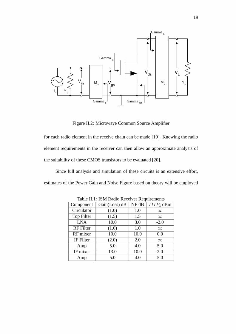
II.3 Application of RF CMOS to ISM Radio
In previous studies, the RF CMOS common source amplifier has been an-
alyzed, modelled, compared to measurement for IIIP3, NF, Power Gain, match-
ing, stability, and SFDR. Now evaluating the applicability of CMOS transistors
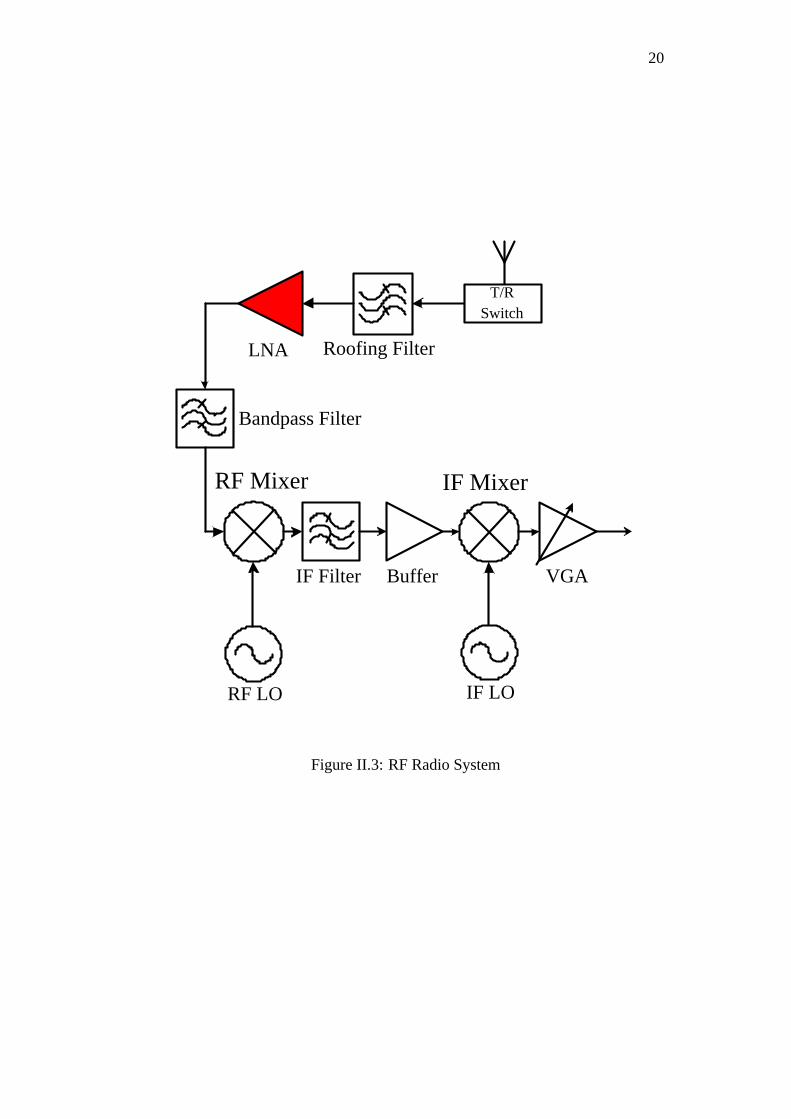
to mobile radio design will complete the study [18]. Referring to Fig. II.3 as an
example of ISM radio architecture, Table II.1 contains a partial list of the ISM ra-
dio receiver requirements, upon which assessing the design requirements needed
Page 41
19
v gs
v ds
M s v in M
L
v L
Y L
Y s
Gamma s
Gamma in
Gamma out
Gamma L
i s
Figure II.2: Microwave Common Source Amplifier
for each radio element in the receive chain can be made [19]. Knowing the radio
element requirements in the receiver can then allow an approximate analysis of
the suitability of these CMOS transistors to be evaluated [20].
Since full analysis and simulation of these circuits is an extensive effort,
estimates of the Power Gain and Noise Figure based on theory will be employed
Table II.1: ISM Radio Receiver RequirementsComponent Gain(Loss) dB NF dB IIIP3 dBmCirculator (1.0) 1.0 ∞Top Filter (1.5) 1.5 ∞
LNA 10.0 3.0 -2.0RF Filter (1.0) 1.0 ∞RF mixer 10.0 10.0 0.0IF Filter (2.0) 2.0 ∞
Amp 5.0 4.0 5.0IF mixer 13.0 10.0 2.0
Amp 5.0 4.0 5.0
Page 42
20
RF LO
IF Filter
RF Mixer
Roofing Filter
Buffer VGA
IF Mixer
LNA
Bandpass Filter
IF LO
T/R Switch
Figure II.3: RF Radio System
Page 43
21
to check the applicability of these CMOS transistors to a ISM Receiver.
From the standpoint of practical design with a 0.35µm gate length common
source amplifier, realizing the highest power Gain, minimum Noise Figure, and
acceptable IIIP3 simultaneously in a circuit design, such as a LNA, is not going
to occur without some trade offs. Most notably, some of the gain will be traded-
off to improve the minimum Noise Figure of the circuit. VSWR and IIIP3 may
also require some loss of gain to meet the LNA objectives for ISM.
The amplifiers in the ISM receiver chain must have at least enough power
Gain to boost the signal attenuation through the filters. Based on what has been
discussed for estimates so far, these CMOS transistors could be used in an ampli-
fier in an ISM transceiver design successfully.
II.4 Summary
In summary, an ISM receiver design has been examined for required per-
formance of power Gain, Noise Figure, and linearity. The estimates of the power
Gain have been made upon simple design models and reported results. Based upon
the above estimates, a ISM receiver design using the CMOS transistors introduced
and studied here is practical, this however does not estimate the considerable ef-
fort necessary to achieve a working example.
Page 44
Chapter III
Device Modelling
III.1 Introduction
The specific performance of an analog circuit is best analyzed for RF circuit
performance such as gain, linearity, power, matching, VSWR, amongst others by
working with the small-signal model of the active or passive, device or devices
in the circuit. For model elements, their dimensions should be small compared
to the wavelength of the operating frequency. If the wavelength is comparable to
the element size, a distributed model must be used [21]. Here, the most important
element of an analog circuit, the amplifier, is analyzed for the large-signal, S-
parameter, and small-signal model parameters. Model performance derived from
these parameters are used in turn to predict the above-mentioned circuit and later
system performance characteristics in Chapters IV:Linearity, V:Noise, VI: Opti-
mum Design for CMOS RF Amplifiers, and VII: LNA Design. Following this
discussion of the amplifier, a discussion of the passive element modelling will oc-
22
Page 45
23
cur. Finally, in Chapter IX: Experimental Verification of Theory, the test results
will be compared to the theory developed in this Chapter III.
III.1.1 Device Theory–A Brief Background
The purpose of this section is to provide a brief background of device physics
theory for the active devices. The two areas of active devices are MOSFET’s and
Heterojunction Bipolar Transistors (HBT’s) and will be reviewed in brief.
Metal Oxide Semiconductor Field Effect Transistors (MOSFET’s)
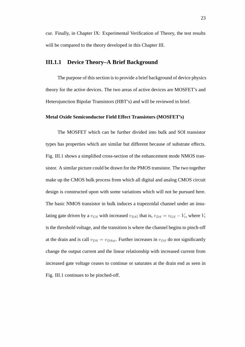
The MOSFET which can be further divided into bulk and SOI transistor
types has properties which are similar but different because of substrate effects.
Fig. III.1 shows a simplified cross-section of the enhancement mode NMOS tran-
sistor. A similar picture could be drawn for the PMOS transistor. The two together
make up the CMOS bulk process from which all digital and analog CMOS circuit
design is constructed upon with some variations which will not be pursued here.
The basic NMOS transistor in bulk induces a trapezoidal channel under an insu-
lating gate driven by a vGS with increased vDS; that is, vDS = vGS − Vt, where Vt
is the threshold voltage, and the transition is where the channel begins to pinch-off
at the drain and is call vDS = vDSat. Further increases in vDS do not significantly
change the output current and the linear relationship with increased current from
increased gate voltage ceases to continue or saturates at the drain end as seen in
Fig. III.1 continues to be pinched-off.
Page 46
24
Figure III.1: Bulk NMOS Transistor Physical Diagram [1]
Next, some of the current-voltage equations describing the NMOS behavior
will be reviewed. In current-voltage relationship seen in III.1, the linear or triode
region behavior is shown, which occurs when vGS ≥ Vt, vDS ≤ vGS − Vt
iD = k′n
(W
L
) [
(vGS − Vt) vDS − 1
2v2
DS
]
(III.1)
The saturated current-voltage equations shown in III.2 describe the NMOS
behavior in saturation where vGS ≥ Vt, vDS ≥ vGS − Vt [1].
iD =1
2k′n
(W
L
)
(vGS − Vt)2 (1 + λvDS) (III.2)
The square law name regarding CMOS I-V can be seen in the current-
voltage relationship where i ∝ v2. The channel length modulation term is λ and
is equal to 1/VA. These equations are only valid in the long-channel operating re-
gion, where Lg >0.5 µm. At shorter gate lengths, the equations are considerably
Page 47
25
more complicated and the reader is referred to [2] for a fuller treatment.
The NMOS small-signal behavior is described by several parameters of
which a few are mentioned here. The transconductance is defined by III.3.
gm =∂iDS
∂vGS
∣∣∣∣∣vGS=VGS
(III.3)
The transconductance shows the small signal slope from gate voltage to
drain current and composes a simple gain equation in the case of a common-
source amplifier, where the gain =−gmro and ro is the small-signal resistance at
the drain.
The output conductance shows the small signal slope form drain to source
and its reciprocal factors into the load total for determining gain and impedance
matching on other RF parameters.
go =∂iDS
∂vDS
∣∣∣∣∣VGS ,VBS
(III.4)
The next small-signal definition amongst others available is the fT , the fre-
quency of unity current gain, as seen in III.5
fT ≈ gm
2π (cgs + cgd + cgb)(III.5)
where cgs is the gate-source capacitance, cgd is the gate-drain capacitance,
and cgb is the gate-bulk capacitance.
The fT defines the frequency where Ai goes to one (Ai = iO/iI). fT is
Page 48
26
a measure of the current gain of a device. This formula should include extrinsic
circuit elements such as Rg but does not, since they often have a small effect.
fmax is a measure of the frequency where the power gain of a amplifying
device is unity:
fmax ≈ fT√
4Rg (gsd + ωT cgd)(III.6)
where Rg is the distributed gate resistance, gsd is the source-drain conduc-
tance, ωT is the frequency of oscillation in radians per second at the fT transistion,
cgd is the gate-drain capacitance [2].
The difference between fT and fmax can be considerable. Several factors,
depending on the values of Rg, gsd, and cgd. Of the two figures of merit, fmax is
the better estimator of the two for RF performance. Proper modelling is critical
for an accurate estimate of fmax [2].
Silicon on Insulator Field Effect Transistors (SOI FET’s)
The Silicon-on-Insulator (SOI) FET for which an example is shown in Fig.
III.2 shows the general cross-section of a MOSFET on an insulator which could
be formed of oxide or sapphire or other insulating material.
One of the key differences from bulk MOSFET’s and the associated equa-
tions describing I-V behavior is that the SOI transistor is completely separate from
near neighbors due to the insulation from the oxide. Another feature is that the
body contact of the MOSFET in SOI is floating. Thus because of charge isola-
Page 49
27
Figure III.2: SOI NMOS Transistor Physical Diagram [2]
tion, kinks may develop in the I-V plots unlike the smooth transitions seen in bulk
CMOS FET’s. The advantages of the SOI FET are the lower parasitic capaci-
tance [3]. As was seen in III.5, the reduction in capacitance increases the fT .
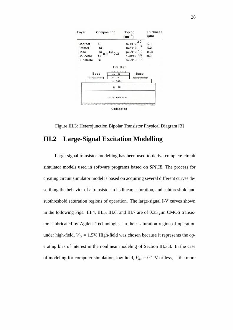
Heterojunction Bipolar Transistors (HBT’s)
The cross-section for the HBT is shown in Fig. III.3. The presence of
Germanium in the base gives the silicon HBT its unique characteristics.
In a Heterojunction device, Germanium added to the base decreases the
bandgap at the emitter-base junction and creates a built-in electric field with the
base [23]. This situation results in improved transport properties through the base
and higher fT and fmax.
This concludes the brief review of device physics of MOSFET’s in bulk
and on-insulator and HBT’s. Much more is available in the literature listed in the
bibliography at the end of the dissertation.
Page 50
28
Figure III.3: Heterojunction Bipolar Transistor Physical Diagram [3]
III.2 Large-Signal Excitation Modelling
Large-signal transistor modelling has been used to derive complete circuit
simulator models used in software programs based on SPICE. The process for
creating circuit simulator model is based on acquiring several different curves de-
scribing the behavior of a transistor in its linear, saturation, and subthreshold and
subthreshold saturation regions of operation. The large-signal I-V curves shown
in the following Figs. III.4, III.5, III.6, and III.7 are of 0.35 µm CMOS transis-
tors, fabricated by Agilent Technologies, in their saturation region of operation
under high-field, Vds = 1.5V. High-field was chosen because it represents the op-
erating bias of interest in the nonlinear modeling of Section III.3.3. In the case
of modeling for computer simulation, low-field, Vds = 0.1 V or less, is the more
Page 51
29
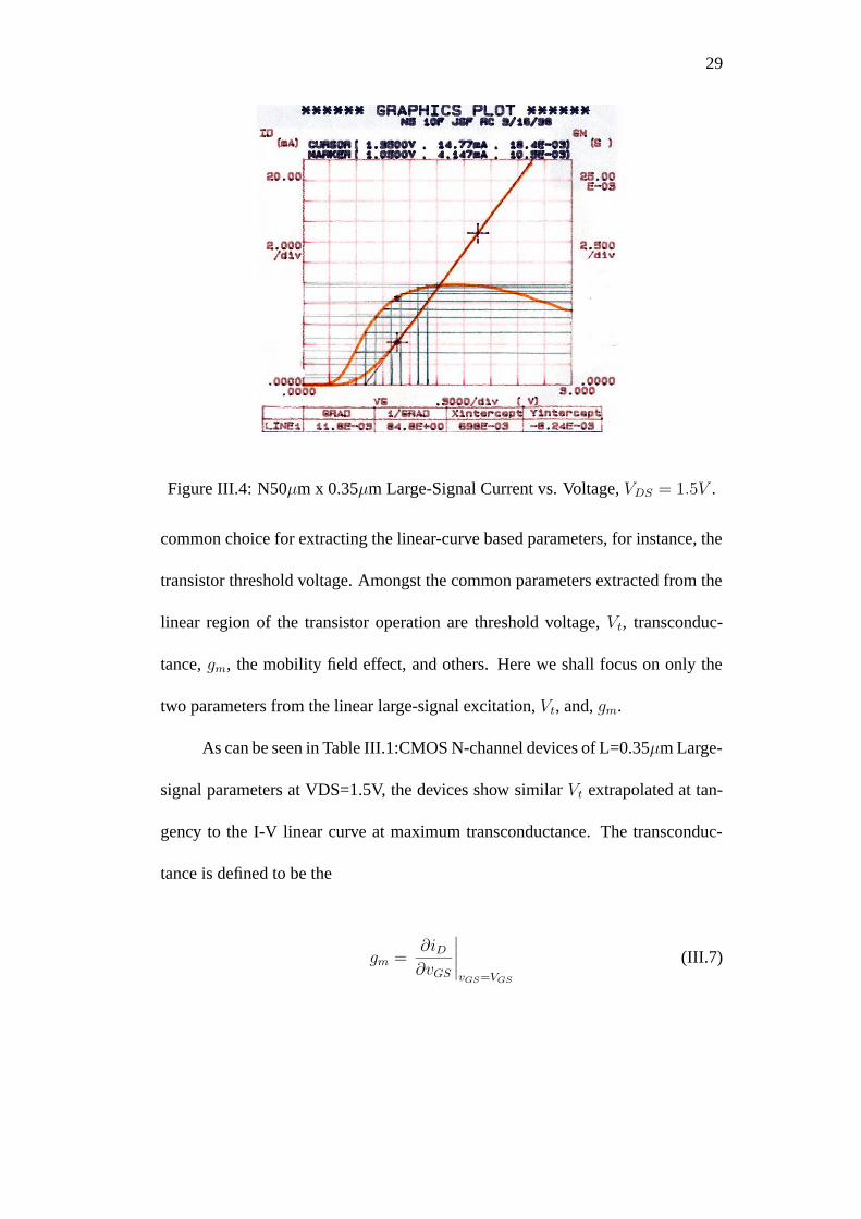
Figure III.4: N50µm x 0.35µm Large-Signal Current vs. Voltage, VDS = 1.5V .
common choice for extracting the linear-curve based parameters, for instance, the
transistor threshold voltage. Amongst the common parameters extracted from the
linear region of the transistor operation are threshold voltage, Vt, transconduc-
tance, gm, the mobility field effect, and others. Here we shall focus on only the
two parameters from the linear large-signal excitation, Vt, and, gm.
As can be seen in Table III.1:CMOS N-channel devices of L=0.35µm Large-
signal parameters at VDS=1.5V, the devices show similar Vt extrapolated at tan-
gency to the I-V linear curve at maximum transconductance. The transconduc-
tance is defined to be the
gm =∂iD∂vGS
∣∣∣∣∣vGS=VGS
(III.7)
Page 52
30
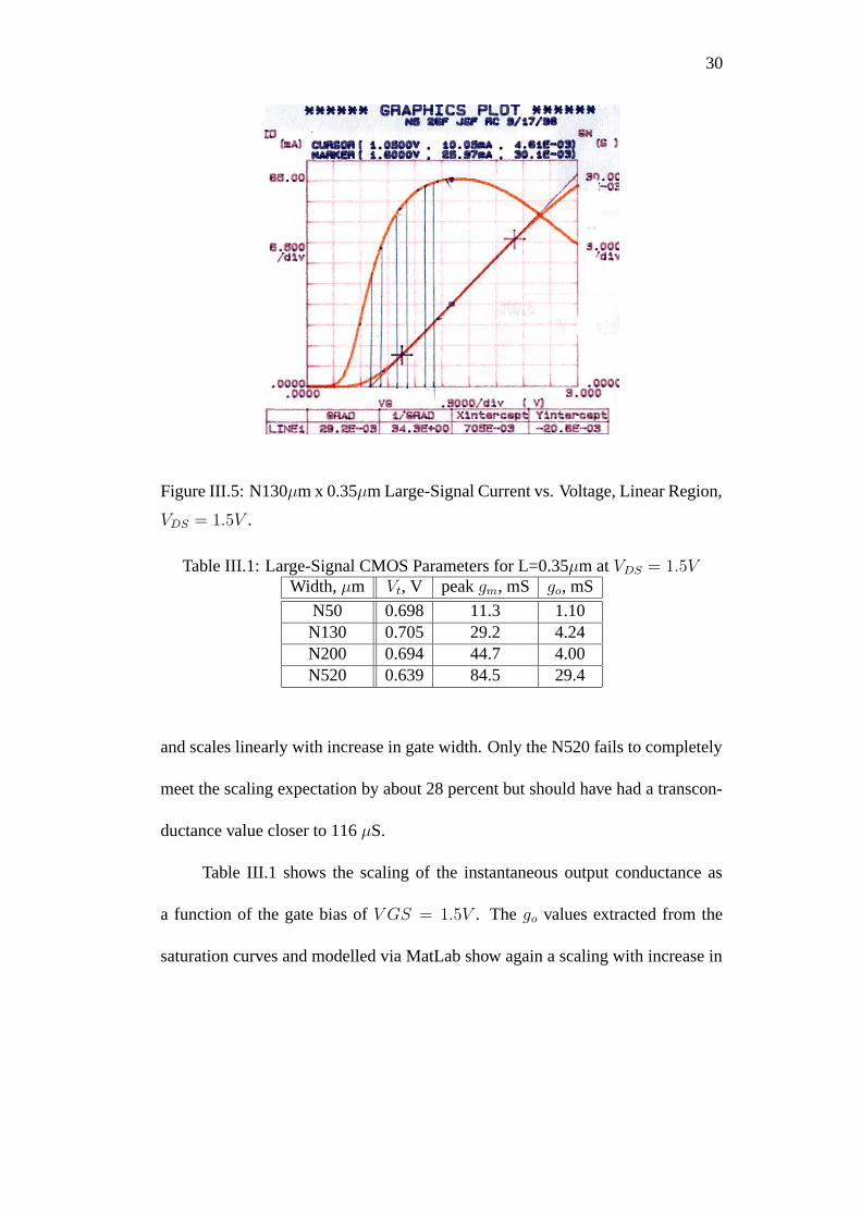
Figure III.5: N130µm x 0.35µm Large-Signal Current vs. Voltage, Linear Region,
VDS = 1.5V .
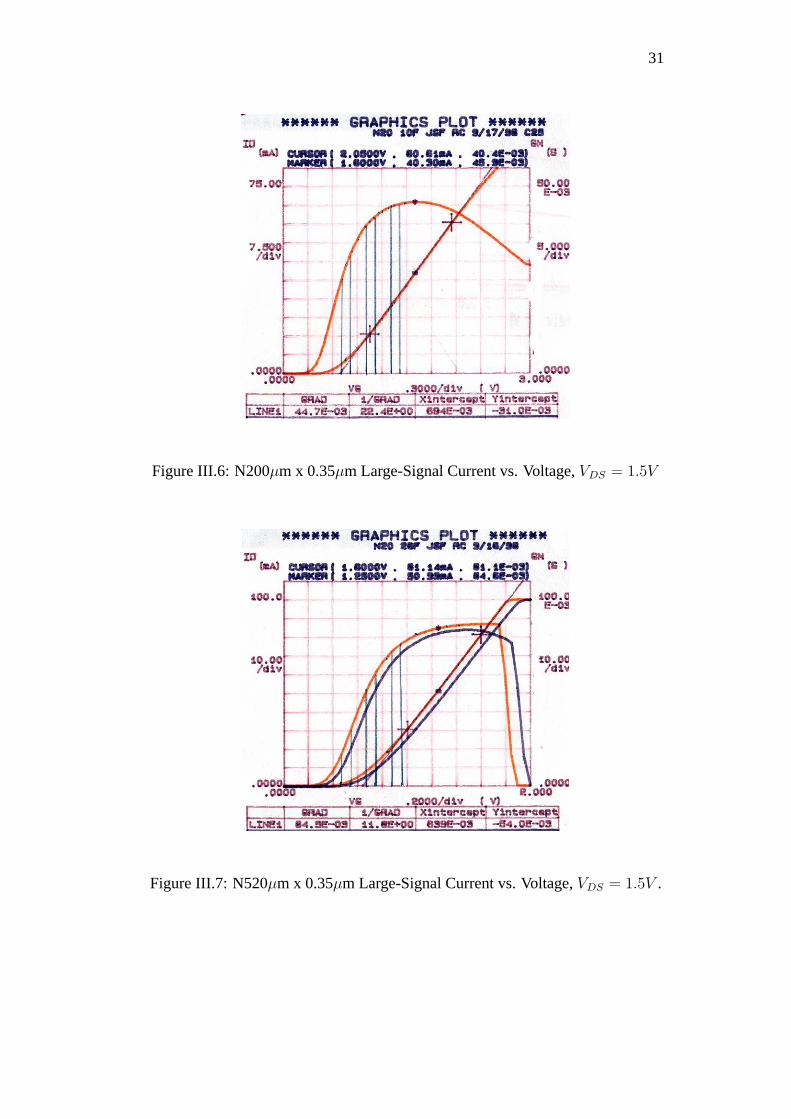
Table III.1: Large-Signal CMOS Parameters for L=0.35µm at VDS = 1.5VWidth, µm Vt, V peak gm, mS go, mS
N50 0.698 11.3 1.10N130 0.705 29.2 4.24N200 0.694 44.7 4.00N520 0.639 84.5 29.4
and scales linearly with increase in gate width. Only the N520 fails to completely
meet the scaling expectation by about 28 percent but should have had a transcon-
ductance value closer to 116 µS.
Table III.1 shows the scaling of the instantaneous output conductance as
a function of the gate bias of V GS = 1.5V . The go values extracted from the
saturation curves and modelled via MatLab show again a scaling with increase in
Page 53
31
Figure III.6: N200µm x 0.35µm Large-Signal Current vs. Voltage, VDS = 1.5V
Figure III.7: N520µm x 0.35µm Large-Signal Current vs. Voltage, VDS = 1.5V .
Page 54
32
Figure III.8: N50µm x 0.35µm Large-Signal Current vs. Voltage, 1.0V ≤ VGS ≤3.0V .
gate width, excepting a fall-off in the larger N520µm transistor.
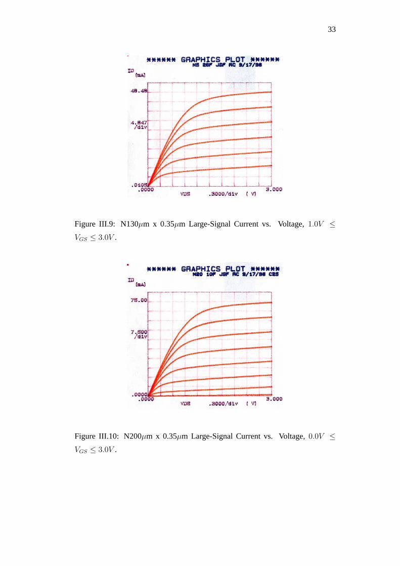
Figs. III.8, III.9, III.10, and III.11 show the N50µm x 0.35µm, N130µm x
0.35µm, N200µm x 0.35µm, and N520µm x 0.35µm transistors saturation perfor-
mance under high-field, Vds = 1.5V . The ro , as defined in III.4, under these con-
ditions is extracted for use in predicting the small-signal performance of intermod-
ulation distortion and other RF characteristics. The values for go as shown in Ta-
ble III.1, are extracted from I-V measurement by taking the derivative of the curve
describing the I-V measurement at a specified VGS over a 1.4V ≤ VDS ≤ 1.6V .
With several points so derived and extracted a function of go vs. VDS can be
plotted. Once plotted, a polynomial function of go can be fitted to the curve vs.
VDS , and coefficients derived for linearity calculations in Chapter IV: Linearity
Page 55
33
Figure III.9: N130µm x 0.35µm Large-Signal Current vs. Voltage, 1.0V ≤VGS ≤ 3.0V .
Figure III.10: N200µm x 0.35µm Large-Signal Current vs. Voltage, 0.0V ≤VGS ≤ 3.0V .
Page 56
34
Figure III.11: N520µm x 0.35µm Large-Signal Current vs. Voltage, 0.3V ≤VGS ≤ 1.5V .
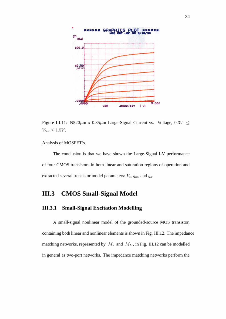
Analysis of MOSFET’s.
The conclusion is that we have shown the Large-Signal I-V performance
of four CMOS transistors in both linear and saturation regions of operation and
extracted several transistor model parameters: Vt, gm, and go.
III.3 CMOS Small-Signal Model
III.3.1 Small-Signal Excitation Modelling
A small-signal nonlinear model of the grounded-source MOS transistor,
containing both linear and nonlinear elements is shown in Fig. III.12. The impedance
matching networks, represented by Ms and ML , in Fig. III.12 can be modelled
in general as two-port networks. The impedance matching networks perform the
Page 57
35
c gd
g m v gs
c gs
1/g m r o c ds
v gs
v ds
M s v s
M L
v L R LOAD
R Source i in
+
-
+
-
+ +
- -
MOSFET
y s
y L
i s
Figure III.12: Simplified small-signal MOSFET model equivalent circuit showing
sources of nonlinear distortion.
function of matching the input or output circuit impedance to the driving or load
impedance by effecting a lossless transformation between the two. That is, the in-
put circuit impedance is matched to the source impedance by the input matching
network and likewise for the output. Of course, the input matching network may
also perform the function of mismatching the input impedance of the circuit to
the source impedance. Similarly, the output matching network can mismatch the
output circuit impedance to the output load. The purposeful mismatching of the
input or output of a circuit will be more fully developed in Chapter VI: Optimum
Design for CMOS RF Amplifiers [22]. The reason for mismatching at source or
load of a two-port amplifier is that the optimum performance of one RF parameter
is often not at the same location on the Smith chart as the others. Thus, a tradeoff
must be to favor one parameter, such as Power Gain, over others, such as NF.
Page 58
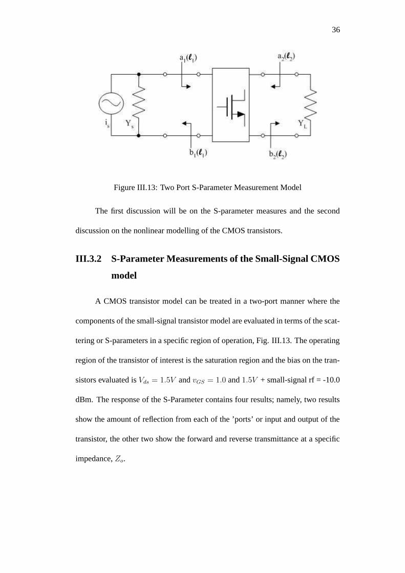
36
Figure III.13: Two Port S-Parameter Measurement Model
The first discussion will be on the S-parameter measures and the second
discussion on the nonlinear modelling of the CMOS transistors.
III.3.2 S-Parameter Measurements of the Small-Signal CMOS
model
A CMOS transistor model can be treated in a two-port manner where the
components of the small-signal transistor model are evaluated in terms of the scat-
tering or S-parameters in a specific region of operation, Fig. III.13. The operating
region of the transistor of interest is the saturation region and the bias on the tran-
sistors evaluated is Vds = 1.5V and vGS = 1.0 and 1.5V + small-signal rf = -10.0
dBm. The response of the S-Parameter contains four results; namely, two results
show the amount of reflection from each of the ’ports’ or input and output of the
transistor, the other two show the forward and reverse transmittance at a specific
impedance, Zo.
Page 59
37
The S-parameters are defined as follows at a specific length from the source
or generator and the load as follows:
S11 =b1a1
∣∣∣∣∣a2=0
(III.8)
S22 =b2a2
∣∣∣∣∣a1=0
(III.9)
The reflection characteristics of the two-port are given in III.8 and III.9 [22].
S21 =b2a1
∣∣∣∣∣a2=0
(III.10)
S12 =b1a2
∣∣∣∣∣a2=0
(III.11)
where the ai and bi are defined as follows and i = 1, 2
ai =V +
i√Zoi
=√
ZoiI+i (III.12)
and
bi =V −
i√Zoi
=√
ZoiI−i (III.13)
The two preceding equations are also functions of position along the waveguide
but this has been suppressed for clarity, [22]. The transmission characteristics of
the two-port are given in III.10 and III.11.
Page 60
38
The results of characterizing CMOS transistors for S-parameters at the bi-
ases described above is given in Chapter IX. S-parameters are widely used to de-
termine matching, gain, linearity, and noise RF parameters and will be discussed
in greater detail in Chapter VI: Optimum Design for CMOS RF Amplifiers.
III.3.3 Modeling of the Nonlinear Elements in the Small-Signal
Model
The nonlinear lumped elements of the small-signal model for the CMOS
transistor can be modelled by terms which describe the performance of each el-
ement from large-signal under different biases. Also, estimates can be made of
the terms describing the lumped element values by calculations based on physical
process data [2, 24].
Under normal operation in the saturation region, the major sources of non-
linearity are the transconductance (gm) , the gate-source capacitance (Cgs) , the
channel conductance (go) and drain-substrate capacitance (Cds) [2]. The gate-
drain capacitance (Cgd) can be considered to be a linear element [2].
We begin with an analysis of the output circuit. The transistor transconduc-
tance can be characterized by a nonlinearity of the following general form [2]
igm = (a1 ∗ vgs + a2 ∗ v2gs + a3 ∗ v3
gs + ...) ∗ (VGS − Vt) (III.14)
where igm is the small-signal output current and vgs is the small-signal input volt-
age. Remembering the definitions for the gate voltage, vGS = VGS + vgs, for the
Page 61
39
total large and small signal, likewise for iGm = IGm + igm. Then the complete
current relationship can be stated as follows
iGm = (a0 + a1 ∗ vgs+ a2 ∗ vgs2 + a3 ∗ vgs3 + ...) ∗ (VGS − Vt) (III.15)
From III.15, the relationship between large and small signal parameters used in
modelling can be clearly seen. The first term in III.15 is the large-signal gm and
the rest are the small-signal terms from a polynomial expansion around a partic-
ular operation point. The drain-source current from this equation is composed
of two sources one representing the small-signal contribution about a large-signal
operating point. If the small-signal were turn-off, then the drain-source current
would be a function of the large-signal gm in product with Veff , where Veff is
equal to VGS − Vt. In the expansion of III.15, finding the small-signal curvature
of the I-V relationship around a given large-signal bias is the desired goal.
Each of the Figs. III.14, III.15, III.16, and III.17 show the modelled transcon-
ductance, gm vs. VGS . Coefficients were derived for each of the nonlinear ele-
ments described by polynomial expansion and fitting about a large-signal operat-
ing point in MatLab based on measured IV curves under specific bias conditions.
Thus, the power series expansion given in III.14, for instance, contains both the
large-signal value of transconductance, a0, and the small-signal value of transcon-
ductance, a1, along with higher orders, an. This provides for prediction of the
transconductance in the presence of both large-signal and small-signal excitation.
The extracted coefficients are shown in Table III.2.
Page 62
40
0.6 0.7 0.8 0.9 1 1.1 1.2 1.3 1.4 1.54
5
6
7
8
9
10
11
12
13x 10
−3
Vgs, V
gm
N50 gm model vs. measured, Vds=1.5V
modelmeasured
Figure III.14: N50µm x 0.35µm Measured and Modelled gm vs. VGS
Table III.2: Transconductance Coefficients for Nonlinear Analysis, gm
gm
NMOS a0(m) a1(m) a2(m) a3(m)N50 9.2 12.4 -5.4 -14.2N130 24.9 19.4 -29.2 18.9N200 38.5 30.3 4.7 27.8N520 102.5 71.0 25.3 -18.5
Page 63
41
0.6 0.7 0.8 0.9 1 1.1 1.2 1.3 1.4 1.50.005
0.01
0.015
0.02
0.025
0.03
0.035
Vgs,V
gm,S
N130 gm Model vs. Measured, Vds = 1.5V
datamodel
Figure III.15: N130µm x 0.35µm Measured and Modelled gm vs. VGS
Page 64
42
0.6 0.7 0.8 0.9 1 1.1 1.2 1.3 1.4 1.50.015
0.02
0.025
0.03
0.035
0.04
0.045
0.05
Vgs,V
gm
N200 gm model vs. measured, Vds=1.5V
modelmeasured
Figure III.16: N200µm x 0.35µm Measured and Modelled gm vs. VGS
Page 65
43
0.6 0.7 0.8 0.9 1 1.1 1.2 1.3 1.4 1.50
0.01
0.02
0.03
0.04
0.05
0.06
0.07
0.08
0.09
Vgs, V
gm
modelmeasured
Figure III.17: N520µm x 0.35µm Measured and Modelled gm vs. VGS
Page 66
44
Similarly, the output conductance can be characterized as
iro= (g1 ∗ vds + g2 ∗ v2
ds + g3 ∗ v3ds + ...) ∗ (VDS) (III.16)
where the quantities g1, g2, and g3 are also functions of vgs and g1 is the linear
small-signal drain-source conductance. The complete small- and large-signal ver-
sion is given in III.16
Iro+ iro
= (g0 + g1 ∗ vds + g2 ∗ v2ds + g3 ∗ v3
ds + ...) ∗ (VDS) (III.17)
In the expansion of III.17, finding the small-signal curvature of the I-V re-
lationship around a given large-signal bias is the desired goal.
Each of the Figs. III.18, III.19, III.20, and III.21 show the modelled out-
put conductance, go vs. VDS . Coefficients were derived for each of the nonlinear
elements described by polynomial expansion and fitting about a large-signal oper-
ating point in MatLab based on measured IV curves under specific bias conditions.
Thus, the power series expansion given in III.16, for instance, contains both the
large-signal value of output conductance, g0, and the small-signal value of out-
put conductance, g1, along with higher orders, gn. This provides for prediction
of the output conductance in the presence of both large-signal and small-signal
excitation. The extracted coefficients are shown in Table III.3.
The output capacitor can be characterized by
icds= c1
dvds
dt+c22
dv2ds
dt+c33
dv3ds
dt+ ... (III.18)
Page 67
45
1.4 1.42 1.44 1.46 1.48 1.5 1.52 1.54 1.56 1.58 1.66.4
6.5
6.6
6.7
6.8
6.9
7
7.1
x 10−3
Vds, V
go, S
N50 go vs. Vds, Vgs=1.5V
datamodel
Figure III.18: N50µm x 0.35µm Measured and Modelled go vs. VDS
Table III.3: Output Conductance, go
go
NMOS g0(m) g1(m) g2(m) g3(m)N50 1.1 -3.52 2.25 -0.7N130 4.2 -6.98 3.25 -50.5N200 4.0 -4.82 7.25 270.9N520 29.4 -16.45 52.4 424.2
Page 68
46
1.4 1.42 1.44 1.46 1.48 1.5 1.52 1.54 1.56 1.58 1.6
0.015
0.0152
0.0154
0.0156
0.0158
0.016
0.0162
N130 go vs. Vds, Vgs=1.5V
Vds, V
go, S
gomodel
Figure III.19: N130µm x 0.35µm Measured and Modelled go vs. VDS
Page 69
47
1.4 1.42 1.44 1.46 1.48 1.5 1.52 1.54 1.56 1.583.7
3.8
3.9
4
4.1
4.2
4.3
4.4x 10
−3 N200 go vs. Vds, Vgs=1.5V
Vds, V
go, S
go
Figure III.20: N200µm x 0.35µm Measured and Modelled go vs. VDS
Page 70
48
1.4 1.42 1.44 1.46 1.48 1.5 1.52 1.54 1.56 1.58 1.6
0.0465
0.047
0.0475
0.048
0.0485
N520 go vs Vds, Vgs=1.5V
Vds, V
go, S
gomodel
Figure III.21: N520µm x 0.35µm Measured and Modelled go vs. VDS
Page 71
49
0.4 0.6 0.8 1 1.2 1.4 1.6 1.8 23.5
3.6
3.7
3.8
3.9
4
4.1x 10
−14
Vds
Cds
Cds vs. Vds at 1.5 Vgs
modeldata
Figure III.22: N50µm x 0.35µm Modelled cDS vs. vDS
Page 72
50
Table III.4: Output Capacitance, cDS
cDS
NMOS c0(f) c1(f) c2(f) c3(f)N50 21.7 -15.65 91.10 5.28N130 83.1 -40.69 236.9 13.73N200 100.0 -62.6 364.4 21.12N520 207.0* -162.8 947.5 424.2
The Fig. III.22 shows the modelled output capacitance, cDS0 vs. vDS . Coefficients
were derived for each of the nonlinear elements described by polynomial expan-
sion and fitting about a large-signal operating point in MatLab based on measured
CV curves under specific bias conditions. Thus, the power series expansion given
in III.18, for instance, contains both the large-signal value of output capacitance,
c0, and the small-signal value of output capacitance, c1, along with higher orders,
cn. This provides for prediction of the output capacitance in the presence of both
large-signal and small-signal excitation. The extracted coefficients are shown in
Table III.4. The relationship between cDS0 and III.18 is that of the capacitance
value of a MOS capacitor at a given large-signal bias. Of course, no large-signal
current flows to contribute to the overall small-signal current in III.18, but the
value of the ’large-signal’ capacitance changes in a MOS capacitor as a function
of the large-signal bias. The measure of the capacitance is found by tying an rf
oscillator to a slow large-signal or dc ramp. In the expansion of III.18, finding the
small-signal curvature of the C-V relationship around a given large-signal bias is
the desired goal.
Page 73
51
0 0.1 0.2 0.3 0.4 0.5 0.6 0.7 0.8 0.9 1 1.1 1.2 1.3 1.4 1.51.5
2
2.5
3
3.5
4
4.5
5
5.5x 10
−14
Vgs, V
Cgs
, F
N50 Cgs vs. Vgs, Vds=1.5V
datamodel
Figure III.23: N50µm x 0.35µm Modelled cGS vs. VGS
The input capacitor current can be modelled by
icgs= cg1
dυgs
dt+cg2
2
dυ2gs
dt+cg3
3
dυ3gs
dt(III.19)
The Figs. III.23, III.24, III.25, III.26 shows the modelled input capacitance, cgs0
vs. VGS . Coefficients were derived for each of the nonlinear elements described by
polynomial expansion and fitting about a large-signal operating point in MatLab
based on measured CV curves under specific bias conditions. Thus, the power
series expansion given in III.19, for instance, contains both the large-signal value
of input capacitance, cg0, and the small-signal value of input capacitance, cg1,
Page 74
52
0 0.5 1 1.54
5
6
7
8
9
10
11
12
13
14x 10
−14
Vgs, V
Cgs
, F
N130 Cgs vs. Vgs, Vds=1.5V
modeldata
Figure III.24: N130µm x 0.35µm Modelled cGS vs. VGS
Page 75
53
0.6 0.7 0.8 0.9 1 1.1 1.2 1.3 1.4 1.51
1.2
1.4
1.6
1.8
2
2.2x 10
−13
Vgs, V
Cgs
, F
N200 Cgs vs. Vgs, Vds=1.5V
datamodel
Figure III.25: N200µm x 0.35µm Modelled cGS vs. VGS
Page 76
54
0 0.5 1 1.5
2
3
4
5
6x 10
−13
Vgs, V
Cgs
, F
N520 Cgs vs. Vgs, Vds=1.5V
datamodel
Figure III.26: N520µm x 0.35µm Modelled cGS vs. VGS
Page 77
55
Table III.5: Input Capacitance, cGS
cGS
NMOS cg0(f) cg1(f) cg2(f) cg3(f)N50 50.9 15.15 -52.0 41.8N130 132.7 42.9 141.8 110.8N200 204.3 -491 628 632N520 681.3 169.5 564.0 442
along with higher orders, cgn. This provides for prediction of the input capacitance
in the presence of both large-signal and small-signal excitation. The extracted
coefficients are shown in Table III.5. The relationship between cGS0 and III.19
is that of the capacitance value of a MOS capacitor at a given large-signal bias.
Of course, no large-signal current flows to contribute to the overall small-signal
current in III.19, but the value of the ’large-signal’ capacitance changes in a MOS
capacitor as a function of the large-signal bias. The measure of the capacitance
is found by tying an rf oscillator to a slow large-signal or dc ramp for large area
capacitors. For small capacitance found in the gates of MOSFET’s, Y-parameters
derived from measured S-parameters of the MOSFET’s were used following a
deembedding process for pad effects. The properly scaled values of capacitance as
a function of area were compared between the measured MOSFET’s and physical
process data, using a CV meter. The body and source of the MOSFET’s is strongly
connected through substrate contacts, thus the two are combined in this study. In
the expansion of III.19, finding the small-signal curvature of the C-V relationship
around a given large-signal bias is the desired goal.
Page 78
56
This concludes the development of the nonlinear description of the CMOS
small-signal model. The coefficient of the polynomial expansions describing the
nonlinear performance of the CMOS small-signal model have derived using Mat-
Lab from measured large-signal IV or CV data and physical process data. These
predicted and derived descriptions for the nonlinear behavior of the CMOS small-
signal model will be used to predict RF characteristics including linearity and
noise whose detailed theoretical development is shown in Chapters IV and V.
III.4 Computer Simulation of Small-Signal Model
The designs for this research program were completed in the Hewlett-Packard’s,
now Agilent Technologies’ (AT), 0.35µm CMOS 14TB process administered through
MOSIS at the University of Southern California, and fabricated at AT’s wafer
foundry in California, USA, with one exception. The AT supplied an HSPICE
BSIM3v1 model based on University of California, Berkeley geometrically en-
hanced SPICE or BSIM model. The CAD software package used in the design
and simulation of the devices and circuits of this research program reported in this
dissertation was Cadence Spectre, excepting one application in Pspice.
III.4.1 CMOS Transistor Simulation Model
In the beginning of the research program, it was desired to use Cadence’s
Spectre RF software design tools based on BSIM3v3 to exploit the nonlinear
Page 79
57
Figure III.27: The Converted Cadence Spectre Transistor Model of AT’s HSPICE
BSIM3v3
Page 80
58
Figure III.28: 2nd Part of The Converted Cadence Spectre Transistor Model of
AT’s HSPICE BSIM3v3
Figure III.29: IBM SOS Transistor Simulation Model
estimation software. Thus a transistor model based upon the physical wafer pro-
cess, in which the design would be carried out, was required. Equivalent mod-
els were created to provide for this need as seen in Figs. III.27 and III.28 from
Hspice BSIM3v1. The main difference between the HSPICE version and the
Cadence Spectre versions are that Cadence model in general does not support di-
mensionally segregated model files. Certain other coefficients in Cadence version
of BSIM3v3 lack temperature dependence as well. The result makes HSPICE a
more device specific transistor model than what Cadence provides.
Pspice was used to simulate a millimeter wave CMOS LNA at 26 to 28 GHz
with models provided by IBM’s 0.15µm wafer foundry in Burlington, Vermont. A
Page 81
59
copy of the models is shown in Fig. III.29. The complete discussion of the design
based on these transistor simulation models is found in Chapter VII: LNA Design
and the performance results are found in Chapter IX: Experimental Verification
of Theory.
III.4.2 RF CMOS Simulation Techniques
While the I-V large-signal simulation of the transistor was successful in Ca-
dence, the RF or small-signal simulation performance at 5.0 GHz was not. That is,
the simulator was able to provide correct I-V curves for the circuits and approx-
imately correct values for Power Gain but could not give reasonable values for
NF and intermodulation distortion. Thus simulation experiments were conducted
to try to improve the transistor simulation by adding additional components to
bring the simulation predictions in line with measured results. This attempt did
not prove successful because of a lack of control offered by Cadence software
over the model and nonlinear calculations. Because the RF simulation linearity
predictions were significantly different than the calculated and measured values
continued work in attempting to improve the performance of Cadence for 5.0 GHz
RF CMOS simulation was stopped in favor of direct theoretical calculation and
measurement. The conclusion was that, without direct control of the modelling
of nonlinear elements in the simulation schematic, little improvement could be
realized further using Cadence RF Spectre tools in this application.
The comparison of measured and simulated results for |S21| shows poor
Page 82
60
Figure III.30: ADS Transistor Simulation Schematic showing additional elements
added for improved RF modeling
Page 83
61
Figure III.31: |S21| ADS Transistor Simulation Prediction Before Model Enhance-
ment. The comparison of measured and simulated results shows poor agreement.
agreement.
The comparison, in Fig. III.32, of measured and simulated results is im-
proved.
However, a different simulator was used called ADS: Advanced Develop-
ment System, which was based on the former AT’s Libra and MDS. The ADS
schematic with the additional circuit components is shown in Fig. III.30 was used
to further understand how much of an improvement in RF simulation could be re-
alized. The results in predicting S-parameter performance versus actual measured
data is shown in Fig. III.31. An improvement is realized with additional external
components to the transistor in the schematic for simulation as seen in Fig. III.32.
The transistor is simulated using the model file described in Subsection III.4.1.
Page 84
62
Figure III.32: Polar plot of |S21| ADS Transistor Simulation Prediction after
Model Enhancement.
Page 85
63
Figure III.33: Seven Turn Spiral Inductor in Metal Four
III.4.3 Passive Element Simulation
The design of RF integrated circuits requires the use of resonating elements
formed as inductors and capacitors. The prediction of the performance of induc-
tors of different shapes was desired to predict the proper matching, quality factor,
and noise of circuit designs. To this end, inductors were designed with layout tools
from Tanner’s L-Edit in top-level metal, level four, of AT’s 0.35µm CMOS 14TB
process, Fig. III.33. The layout file was imported to Sonnet’s Electromagnetic
Simulator for prediction of inductance. The attempt to run the electromagnetic
simulation on a Sun/Solaris Ultra 1 as seen in Fig. III.34 failed because of the
required memory capacity for the matrix element partitioning of the inductor was
exceeded significantly. Changes to the partitioning size did result in a reduced
memory requirement and thus a lowered estimated run-time but also a significant
increase in the error of the current density desired for inductance predictions. The
run time estimates were in weeks of time.
The use of another electromagnetic simulator, Fast Henry, was also unsuc-
Page 86
64
Figure III.34: Sonnet Run File for Spiral Inductance Prediction
Page 87
65
cessful. The problem of Finite Element Method (FEM) in predicting small in-
ductances from large integrated circuit metal area creates for both programs very
large matrix sets, which require large computer resource to store and calculate.
The software programs, Sonnet and Fast Henry, were created for macro-level and
board-level simulations of inductance amongst other physical parameters. How-
ever, the problem of adapting the algorithms in these two programs to integrated
circuit level simulations on desk-top computers is more demanding.
Thus the inductance of spiral metal layouts is predicted from geometrical
formula in III.20. The results of the inductor and capacitor designs is compared
to the predictions of III.20 in Chapter IX: Experimental Verification of Theory.
L ≈ 45µ0n2a2
22r − 14a(III.20)
The r is the outer radius of the spiral, a is the mean radius of the spiral, µ0 is
the permeability of free space, n is the number of turns. This formula produces an
estimate of 5 nH for the seven-turn inductor and 2 nH for the three-turn inductor
[25].
III.5 Device Design of Experiment
In order to check the validity of the theoretical predictions made in this
chapter, passive and active circuit elements are designed. The first experiment
designed was to evaluate resonant passive elements for the Quality Factor and
Page 88
66
Table III.6: Design of Experiment II: InductorsInductor 7-turn 3-turn
Substrate√ √
Metal 1√ √
N-well√ √
Metal 1/N-well√ √
performance as a function of design layout geometry, DOE II. The different cate-
gories of inductors composed an experiment, where the effects of shielding of the
inductor from the eddy currents in the conductive substrate via metal 1 and n-well,
could be checked.
One metal plate capacitor is included in this DOE II. The inductors and
capacitor were measured and will be reported on in Chapter IX: Experimental
Verification of Theory.
In DOE III additional inductors, shown in Table III.8, of seven- and three-
turn were added to the test transistors listed in Table III.7. Also four MOS ca-
pacitors, improved calibration structures, and an LNA were added to the layout
design. The transistor set of DOE III make up a design of experiment over gate
structure by varying gate width and finger number. One common-gate design is
included.
The inductor set of DOE III is different than DOE II where the shielding ef-
fectness of lower process layers to top level metal is studied. In this process metal
four is the top level metal and shielding it to eddy currents in the lossy substrate
of bulk CMOS is desired. The different categories of inductors composed an ex-
Page 89
67
Table III.7: Test Transistor GeometryDevice Gate Finger Width in µm Number of Fingers
N50 5 10N200 20 10N130 5 26N520 20 26
Table III.8: Design of Experiment III: InductorsInductor 7-turn 3-turn
Substrate√ √
N-well√ √
Fractured N-well√ √
Fractured Poly/N-well√ √
Fractured Metal 1/N-well√ √
Fractured Poly√ √
Fractured Metal 1√ √
periment, where the effects of shielding of the inductor from the eddy currents
in the conductive substrate via polysilicon and n-well, could be checked. What
is unknown and difficult to predict is the benefit of shielding the top-level metal
from the lossy substrate to improve the Q of the inductors designed in this process.
This is shown in Table III.8.
The capacitor set of DOE III is designed four MOS capacitors of increasing
area to determine the scaling of capacitance as a function of junction area.
Transformers, inductors, and calibration structures are designed in DOE V
with power amplifier designs in the Agilent Technologies (AT) 0.55µm CMOS
process. The purpose of including transformers in DOE V was to determine there
performance for use in a mixer design.
Page 90
68
Table III.9: Test Capacitor GeometryDevice Area in µm2
MOS1 630MOS2 1206MOS3 2440MOS4 5040
Table III.10: Design of Experiment V: InductorsInductor 3-turn
Substrate√
Poly, Fine Mesh√
Poly, Medium Mesh√
Poly, Finger narrow wide√
Poly, Finger wide with center taps√
N-well mesh√
No center tap√
The DOE V allows determination of the efficacy of different shielding for
inductors in the Agilent Technologies (AT) 0.55µm CMOS process as described
in Table VIII.5.
The transformer DOE provides a means of measuring the scaling as a func-
tion of transformer turns ratio as seen in Table VIII.6.
Table III.11: Design of Experiment V: TransformersTransformers over Poly, Medium Mesh Ratio
XTRM1 1:1XTRM2 1:3XTRM3 1:5
Page 91
69
III.6 Summary
The mathematical and computer modelling of both devices and transis-
tors has been reviewed in preparation for theoretical RF predictions and design
work presented in later chapters. The use of large-signal data for deriving ba-
sic CMOS transistor modelling has been made. The use of small-signal data from
S-parameters has been defined for later predictions of RF CMOS transistor perfor-
mance. The use of small-signal data for deriving nonlinear polynomial expansions
has been shown and will be employed to predict linearity in Chapter IV: Linearity
and noise in Chapter V: Noise. The construction of transistor models for com-
puter simulation based on physical processes has been described and reviewed.
The attempt to use Finite Element Matrix methods to predict inductance has been
reviewed, followed by geometrical prediction of spiral inductors.
The text of this chapter, in part, is a reprint of the material as it appears in our
published papers in IEEE Conferences [SiRF03, Germany; IEDM99, USA] and
in preparation for Conferences and Transactions on Microwave Theory and Tech-
niques. The dissertation author was the primary investigator and primary and
secondary author of these papers.
Page 92
Chapter IV
Linearity Analysis of MOSFET’s
IV.1 Introduction
Intermodulation distortion is the key limitation on the dynamic range per-
formance of a small-signal amplifier under large-signal conditions. Our goal here
is to predict the nonlinear behavior, particularly third-order intermodulation dis-
tortion, as a function of device design, biasing, and impedance termination. The
results can then be used in conjunction with the noise model of the device to opti-
mize the dynamic range of an RF receiver [26, 27].
The intermodulation distortion is the result of a weakly nonlinear small-
signal problem, in which the situation of multiple small-signal excitations is stud-
ied. The excitations are in-band and therefore nonfilterable. Understanding how
to predict the presence of the nonlinearity improves the overall design objec-
tives of making better radio receivers by increasing the Spur-Free Dynamic Range
(SFDR). In-band unwanted distortion arises from many sources which can gener-
70
Page 93
71
ally be referred to as spurious. The effect of the presence of spurious responses is
to desensitize the receiver to a desired signal [28].
The many ways in which spurious responses are accounted for through coin-
cidence and congruence of intermodulation frequencies is an extensive calculation
which will not be shown here. Coincidence occurs when undesired intermodula-
tion coincides with an IF output. Congruence occurs when undesired intermodu-
lation occurs at the same value of an IF. These two mechanisms yield a reduction
in IF selectivity and RF sensitivity for which an accounting method can generate
a trouble list of interference modes [29].
A way of reducing the likelihood of such problems is to understand linear-
ity as a figure of merit (FOM) based on the two-toned test. This test measures
the response of an amplifier at its output to two slightly separated tones of equal
magnitude at its input. The two tones at the input will re-appear at the output with
harmonics of the two tones based on weakly nonlinear behavior of the amplifier.
The separation of the fundamental tones from the odd harmonics at the output is
the measure of the linearity of an amplifier. An amplifier is the basic circuit ele-
ment of the all analog/RF design, it arises in LNA’s, VGA’s, Mixer’s, and buffers,
amongst other examples.
If the combination of closely separated frequencies is examined, odd mul-
tiples will appear close to the fundamental, such as f1 and f2, whose odd-order
intermodulation products (IMP), are 2f2−f1 and 2f1−f2. Even-order IMP are far
Page 94
72
Weakly Nonlinear Circuit S i S o
Figure IV.1: Weakly Nonlinear Block Diagram.
removed from the original two frequencies applied at the input and are therefore
filterable [29].
A powerful technique for analyzing the weakly nonlinear small-signal prob-
lem is a Volterra Analysis [26]. Volterra analysis does not make requirements on
the circuit model to have separable memoryless nonlinear elements and frequency-
sensitive linear components, as in power series analysis. The Volterra analy-
sis could be compared to a transfer function where the phase and amplitude are
changed as a result of the application of the function. Or, nonlinear circuit anal-
ysis could be used where the circuit components have nonlinear expressions for
which the coefficients of the polynomial expansion of the nonlinearity can be de-
termined. This analysis is used in the following sections of this chapter and could
be applied a KCL or a KVL analyses of a circuit [26, 28]. The nonlinear circuit
components can be resistive, reactive, or a combination. The basic model is shown
in Fig. IV.1.
Volterra Analysis has in recent years been applied at 5 GHz to Si BJT’s
Page 95
73
in [27] using a gm nonlinearity, and in Si CMOS [30, 31] by using four nonlin-
ear small-signal model components. Additional analyses, using Volterra anal-
ysis and multiple non-linear small-signal model components, based on SiGe or
GaAS FET’s are yet to be performed and reported. Intermodulation Distortion has
largely been reported in other circuit constructions in the literature by measure-
ment and without prior analysis and simulation. This work in part is the next step
in expanding markedly the robust application of theoretical constructs in Volterra
Analysis to ISM-band RF circuits operating under the constraint of minimized
power dissipation.
Finally, while the general solution for a two-port network in this situation is
very complex, a careful application of Volterra Series Analysis under narrowband
conditions with attention to the harmonics of the impedance values will yield ac-
curate results. We shall first examine the case where the effect of shunt feedback
is missing, Cgd = 0 , in Section IV.2, and then examine the more general case of
including shunt feedback, Cgd, on linearity in Section IV.3, and finally we shall
compare the theoretical predictions to measurement in Chapter IX: Experimental
Verification of Theory.
Page 96
74
c gd
g m v gs
c gs
1/g m r o c ds
v gs
v ds
M s v s
M L
v L R LOAD
R Source i in
+
-
+
-
+ +
- -
MOSFET
y s
y L
i s
Figure IV.2: Simplified small-signal MOSFET model equivalent circuit showing
sources of nonlinear distortion.
IV.2 Grounded-Source Nonlinear Transfer Function
of Output Circuit
Using the nonlinear element description of Chapter III in Sec. III.3.3, and
the Volterra formalism [26] for the output voltage in terms of the input voltage at
the gate yields
vds = H1 vgs +H2 v2gs +H3 v3
gs + ... (IV.1)
and solving for the first order nonlinear transfer function yields
H1(ωa) =−a1
g1 + yL(ωa) + jωac1(IV.2)
where yL is the load impedance in Fig. IV.2. The load impedance is determined
by the matching network, ML, and RLOAD.
The second order transfer function is
Page 97
75
H2(ωa, ωb)
=−(
a2 + g2 ∗ H1(ωa)H1(ωb) + c22j(ωa + ωb) H1(ωa)H1(ωb)
)
g1 + c1j(ωa + ωb) + yL(ωa + ωb)
=−(
a2 +
g2 + c22j(ωa + ωb)
∗ H1(ωa)H1(ωb))
g1 + c1j(ωa + ωb) + yL(ωa + ωb)
=
−
a2 +
g2 + c22j(ωa + ωb)
∗
a21
g1+yL(ωa)+c1jωag1+yL(ωb)+c1jωb
g1 + c1j(ωa + ωb) + yL(ωa + ωb)
(IV.3)
The third-order nonlinear transfer function is more involved. Solving for KCL in
the small-signal model Fig. IV.2 yields:
a3 ∗ υ3gs +
g1 ∗
H3 υ3gs
+
g2 ∗
H1 υgs +H2 υ2gs
2+
g3 ∗ H1 υgs3 +
c1d
dt
H3 υ3gs
+
c22
d
dt
H1 υgs +H2 υ2gs
2+
c33
d
dtH1 υgs3 +
yL
H3 υ3gs
= 0 (IV.4)
Page 98
76
which can be expanded to be
a3 ∗ υ3gs +
g1 ∗
H3(ωa, ωb, ωc) υ3gs
+
2g2 ∗
H1(ωa)H2(ωb, ωc) υ3gs
+
g3 ∗
H1(ωa)H1(ωb)H1(ωc) υ3gs
+
c1j (ωa + ωb + ωc)
H3(ωa, ωb, ωc) υ3gs
+
c2j (ωa + ωb + ωc)
H1(ωa)H2(ωb, ωc) υ3gs
+
c33j (ωa + ωb + ωc)
H1(ωa)H1(ωb)H1(ωc) υ3gs
+
yL (ωa + ωb + ωc)
H3(ωa, ωb, ωc) υ3gs
= 0 (IV.5)
where [26]
H1(ωa)H2(ωb, ωc) =
1
3[H1(ωa)H2(ωb, ωc) +H1(ωb)H2(ωa, ωc) +H1(ωc)H2(ωa, ωb)] (IV.6)
which can be further simplified to be
g1 + c1j (ωa + ωb + ωc) + yL (ωa + ωb + ωc) H3(ωa, ωb, ωc) =
−
a3 + 2g2 ∗
H1(ωa)H2(ωb, ωc)
+ g3 ∗ H1(ωa)H1(ωb)H1(ωc)
+c2j (ωa + ωb + ωc)
H1(ωa)H2(ωb, ωc)
+ c33j (ωa + ωb + ωc) H1(ωa)H1(ωb)H1(ωc)
(IV.7)
and finally
H3(ωa, ωb, ωc) =
Page 99
77
−
a3 + 2g2 ∗
H1(ωa)H2(ωb, ωc)
+ g3 ∗ H1(ωa)H1(ωb)H1(ωc)
+c2j (ωa + ωb + ωc)
H1(ωa)H2(ωb, ωc)
+ c33j (ωa + ωb + ωc) H1(ωa)H1(ωb)H1(ωc)
g1 + c1j (ωa + ωb + ωc) + yL (ωa + ωb + ωc)
(IV.8)
which can be simplified to be
H3(ωa, ωb, ωc) =
−
a3 + (2g2 + c2j (ωa + ωb + ωc)) ∗
H1(ωa)H2(ωb, ωc)
+(
g3 + c33j (ωa + ωb + ωc)
)
∗ H1(ωa)H1(ωb)H1(ωc)
g1 + c1j (ωa + ωb + ωc) + yL (ωa + ωb + ωc)(IV.9)
where the permutation of H1(ωa) and H2(ωb, ωc) was defined in IV.6 [26].
IV.2.1 Grounded-Source Nonlinear Transfer Function of In-
put Circuit
Next, we analyze the input circuit which consists of the linear input source
ys , and the nonlinear capacitance Cgs , as shown in Fig. IV.2. The current through
the input capacitor can be expressed by
icgs= cg1
dυgs
dt+cg2
2
dυ2gs
dt+cg3
3
dυ3gs
dt(IV.10)
Now, using the Volterra formalism for the gate voltage in terms of the source
current yields
vgs = G1 is +G2 i2s +G3 i3s (IV.11)
Page 100
78
and solving at the input node yields
−is + cg1dυgs
dt+cg2
2
dυ2gs
dt+cg3
3
dυ3gs
dt+ ysυgs = 0 (IV.12)
Now, expanding [IV.12]
−is +
cg1d
dt
G1 is +G2 i2s +G3 i3s
+
cg2
2
d
dt
G1 is +G2 i2s +G3 i3s2
+
cg3
3
d
dt
G1 is +G2 i2s +G3 i3s3
+
ys
G1 is +G2 i2s +G3 i3s
= 0 (IV.13)
Now, we can equate terms to find the Volterra G coefficients. Equating first-order
terms, we obtain
−is + cg1d
dtG1 is + ys G1 is = 0 (IV.14)
which implies that
−1 + cg1jωa G1 + ys G1 = 0 (IV.15)
or
G1(ωa) =1
ys(ωa) + cg1jωa
(IV.16)
Equating second-order terms, we get
cg1d
dt
G2 i2s
+cg2
2
d
dtG1 is2 + ys
G2 i2s
= 0 (IV.17)
Page 101
79
and
cg1d
dt
G2(ωa, ωb) i2s
+cg2
2
d
dt
G1(ωa)G1(ωb) i2s
+
ys
G2(ωa, ωb) i2s
= 0 (IV.18)
which further implies that
cg1j(ωa + ωb)
G2(ωa, ωb) i2s
+
cg2
2j(ωa + ωb)
G1(ωa)G1(ωb) i2s
+
ys(ωa + ωb)
G2(ωa, ωb) i2s
= 0 (IV.19)
which implies that
cg1j(ωa + ωb) + ys(ωa + ωb) G2(ωa, ωb) =
−cg2
2j(ωa + ωb) G1(ωa)G1(ωb) (IV.20)
which finally implies that
G2(ωa, ωb) =− cg2
2j(ωa + ωb)G1(ωa)G1(ωb)
cg1j(ωa + ωb) + ys(ωa + ωb)(IV.21)
This can be further reduced to
G2(ωa, ωb) =
− cg2
2j(ωa + ωb)
cg1j(ωa + ωb) + ys(ωa + ωb)ys(ωa) + cg1jωays(ωb) + cg1jωb(IV.22)
Equating third-order terms yields:
cg1d
dt
G3 i3s
+
Page 102
80
cg2
2
d
dt
G1 is +G2 i2s2
+
cg3
3
d
dtG1 is3 +
ys
G3 i3s
= 0 (IV.23)
which can be expanded to be
cg1j (ωa + ωb + ωc)
G3(ωa, ωb, ωc) i3s
+
cg2j(ωa + ωb + ωc)
G1(ωa)G2(ωb, ωc) i3s
+
cg3
3j (ωa + ωb + ωc)
G1(ωa)G1(ωb)G1(ωc) i3s
+
ys (ωa + ωb + ωc)
G3(ωa, ωb, ωc) i3s
= 0 (IV.24)
which can be further simplified to be
G3(ωa, ωb, ωc) =
−
cg2j(ωa + ωb + ωc)
G1(ωa)G2(ωb, ωc)
+
cg3
3j (ωa + ωb + ωc) G1(ωa)G1(ωb)G1(ωc)
cg1j (ωa + ωb + ωc) + ys (ωa + ωb + ωc)
(IV.25)
which, when expanded yields
G3(ωa, ωb, ωc) =
Page 103
81
−
cg2j(ωa + ωb + ωc)
G1(ωa)G2(ωb, ωc)
+
cg3
3j (ωa + ωb + ωc)
G1(ωa)G1(ωb)G1(ωc)
cg1j (ωa + ωb + ωc) + Ys (ωa + ωb + ωc)
(IV.26)
IV.2.2 Total Nonlinear Transfer Function
Next, we calculate the complete transfer function without Cgd feedback.
Now, the total transfer function K is the product of the two transfer functions H
and G. So,
vds = H1 G1 is +G2 i2s +G3 i3s +
H2 G1 is +G2 i2s +G3 i3s2 +
H3 G1 is +G2 i2s +G3 i3s3 (IV.27)
or
vds = K1 is +K2 i2s +K3 i3s + · · · (IV.28)
Equating first order terms we get
vds = H1 G1 is (IV.29)
Page 104
82
K1(ωa) =−a1
g1 + yL(ωa) + c1jωays(ωa) + cg1jωa(IV.30)
This is the first-order transfer function.
Now equating the second-order terms we get
vds = H1 G2 i2s + H2 G1 is2 (IV.31)
which leads to
K2(ωa, ωb) i2s = H1(ωa + ωb) G2(ωa, ωb) i2s +
H2(ωa, ωb) G1(ωa)G1 (ωb) i2s (IV.32)
and finally
K2(ωa, ωb) = H1(ωa + ωb)G2(ωa, ωb) +
H2(ωa, ωb)G1(ωa)G1(ωb) (IV.33)
which, yields
K2(ωa, ωb) =
a1 cg2
2j(ωa + ωb)
g1 + yL(ωa + ωb) + c1j(ωa + ωb)
cg1j(ωa + ωb) + ys(ωa + ωb)
ys(ωa) + cg1jωa ys(ωb) + cg1jωb
−
Page 105
83
a2 +
g2+c22
j(ωa+ωb)a21
g1 + yL(ωa) + c1jωa
g1 + yL(ωb) + c1jωb
g1 + c1j(ωa + ωb) + yL(ωa + ωb)
ys(ωa) + cg1jωa ys(ωb) + cg1jωb(IV.34)
which can be somewhat simplified to be
K2(ωa, ωb) =
[
a1 cg2
2j(ωa + ωb)
]
−
a2 +
g2+c22
j(ωa+ωb)a21
g1 + yL(ωa) + c1jωa
g1 + yL(ωb) + c1jωb
∗
cg1j(ωa + ωb) + ys(ωa + ωb)
g1 + yL(ωa + ωb) + c1j(ωa + ωb) ∗
cg1j(ωa + ωb) + ys(ωa + ωb) ∗
ys(ωa) + cg1jωa ys(ωb) + cg1jωb
Page 106
84
(IV.35)
Now equating third-order terms,
vds = H1
G3 i3s
+H2
G1 is +G2 i2s2
+H3 G1 is3 (IV.36)
This then becomes
vds = H1(ωa + ωb + ωc)
G3(ωa, ωb, ωc) i3s
+
H2(ωa, ωb + ωc) 2
G1(ωa)G2(ωb, ωc) i3s
+
H3(ωa, ωb, ωc)
G1(ωa)G1(ωb)G1(ωc) i3s
(IV.37)
K3(ωa, ωb, ωc) = H1(ωa + ωb + ωc) G3(ωa, ωb, ωc) +
H2(ωa, ωb + ωc) 2
G1(ωa)G2(ωb, ωc)
+
H3(ωa, ωb, ωc) G1(ωa)G1(ωb)G1(ωc) (IV.38)
Next,
K3(ωa, ωb, ωc) = H1(ωa + ωb + ωc) G3(ωa, ωb, ωc) +
2/3H2(ωa, ωb + ωc) G1(ωa)G2(ωb, ωc) +
2/3H2(ωb, ωa + ωc) G1(ωb)G2(ωa, ωc) +
2/3H2(ωc, ωa + ωb) G1(ωc)G2(ωa, ωb) +
H3(ωa, ωb, ωc) G1(ωa)G1(ωb)G1(ωc) (IV.39)
At this point, the algebra is extremely complex. To simplify the analysis,
we assume that we are doing a two-tone intermodulation distortion test; so that,
ωa = ω1, ωb = ω1, and ωc = −ω2 and |ω1| ≈ |ω2|.
Page 107
85
Since the sum of frequency in first two H2 terms of IV.39 produce zero for the
second term of H2, and thus the transfer functions become independent of fre-
quency or dc or large-signal values, not in the frequency band of prediction, the
G2 terms go to zero. Then, with two of the three H2 terms in IV.39 collapsing
with the above substitutions, we get,
K3(ω1, ω1,−ω2) = H1(ω1) G3(ω1, ω1,−ω2) +
2/3H2(−ω2, 2ω1) G1(−ω2)G2(ω1, ω1) +
H3(ω1, ω1,−ω2)
G1(ω1)2G1(−ω2)
(IV.40)
where from IV.9 and substituting in the above,
H3(ω1, ω1,−ω2)
=
−
a3 + (2g2 + c2j (ω1)) ∗
H1(ω1)H2(ω1,−ω2)
+(
g3 + c33j (ω1)
)
∗ H1(ω1)H1(ω1)H1(−ω2)
g1 + c1j (ω1) + yL (ω1)(IV.41)
and
H2(ω1, ω1) =
[
a2 (g1 + yL(ω1) + c1jω1)2]
+ a21
[
g2 + c22j(2ω1)
]
[g1 + c1j(2ω1) + yL(2ω1)] (g1 + c1j(ω1) + yL(ω1))2 (IV.42)
and
H2(ω1,−ω2)
=− [a2 (g1 + yL(ω1) + c1jω1 g1 + yL(−ω2) − c1jω2)] + a2
1 [g2]
[g1] (g1 + yL(ω1) + c1jω1 g1 + yL(−ω2) − c1jω2)
(IV.43)
Page 108
86
and
H2(−ω2, 2ω1) =
a2 (g1 + yL(−ω2) − c1jω1)
(g1 + yL(2ω1) + c1j2ω1)
+ a21
[
g2 + c22jω1
]
[g1 + c1j(2ω1) + yL(2ω1)] ∗
(g1 + c1j(ω1) + yL(ω1)) (g1 − c1j(ω2) + yL(−ω2))
(IV.44)
and with
H1 (ω1)H2 (ω1,−ω2) =
1
3[2H1 (ω1)H2 (ω1,−ω2) +H1 (−ω2)H2 (ω1, ω1)]
(IV.45)
A fairly complete derivation of Hi where i = 1, 2, 3 Volterra transfer functions for
the output have been derived. Now, we need to calculate G2 and G3 with ω1 and
ω2 substituted in. The Gi, where i = 1, 2, 3 Volterra Transfer functions represent
the input nonlinearities, as follows:
G2(ω1, ω1) =−cg2j(ω1)
cg1j(2ω1) + ys(2ω1) (ys(ω1) + cg1jω1)2 (IV.46)
G3(ω1, ω1,−ω2) =
Page 109
87
−
−2/3
cg2j(ω1)2 +
cg3
3j (ω1)
cg1j(2ω1) + ys(2ω1)
ys(−ω2) − cg1jω2 cg1j(2ω1) + ys(2ω1)
ys(ω1) + cg1jω13
(IV.47)
which can be further simplified to
G3(ω1, ω1,−ω2) =
−
−2/3
cg2j(ω1)2 +
cg3
3j (ω1)
cg1j(2ω1) + ys(2ω1)
ys(−ω2) − cg1jω2 cg1j(2ω1) + ys(2ω1) ∗
ys(ω1) + cg1jω13
(IV.48)
and so the final transfer function, with many of the above derived equations, sub-
stituted into IV.40 is
K3(ω1, ω1,−ω2) =
−a1
g1 + yL(ω1) + c1jω1
−
−1/3
cg2j(ω1)2 +
cg3
3j (ω1)
∗
cg1j(2ω1) + ys(2ω1)
ys(−ω1) − cg1jω1 cg1j(2ω1) + ys(2ω1) ∗
ys(ω1) + cg1jω13
+
Page 110
88
2/3
[a2 (g1 + yL(−ω2) − c1jω1) (g1 + yL(2ω1) + c1j2ω1)] +
a21
[
g2 + c22jω1
]
[g1 + c1j(2ω1) + yL(2ω1)] (g1 + c1j(ω1) + yL(ω1)) ∗
(g1 − c1j(ω2) + yL(−ω2))
∗
1
ys(−ω2) − cg1jω2
− cg2
2j(2ω1)
cg1j(2ω1) + ys(2ω1) ys(ω1) + cg1jω12
+
−
a3 + (2g2 + c2j (ω1)) ∗
H1(ω1)H2(ω1,−ω2)
+(
g3 + c33j (ω1)
)
∗ H1(ω1)H1(ω1)H1(−ω2)
g1 + c1j (ω1) + yL (ω1)
∗
(
1
ys(ω1) + cg1jω1
)2 (1
ys(−ω2) − cg1jω2
)
(IV.49)
which can be further expanded to
K3(ω1, ω1,−ω2) =
−a1
g1 + yL(ω1) + c1jω1
∗
−
[−1/3
cg2j(ω1)2 +
cg3
3j (ω1)
cg1j(2ω1) + ys(2ω1)]
ys(−ω1) − cg1jω1 cg1j(2ω1) + ys(2ω1) ys(ω1) + cg1jω13
+
2/3
[a2 (g1 + yL(−ω2) − c1jω1) (g1 + yL(2ω1) + c1j2ω1)] +
a21
[
g2 + c22jω1
]
[g1 + c1j(2ω1) + yL(2ω1)] (g1 + c1j(ω1) + yL(ω1)) ∗
(g1 − c1j(ω2) + yL(−ω2))
∗
Page 111
89
1
ys(−ω2) − cg1jω2
− cg2
2j(2ω1)
cg1j(2ω1) + ys(2ω1) ys(ω1) + cg1jω12
+
−
a3 + (2g2 + c2j (ω1)) ∗
13[2H1 (ω1)H2 (ω1,−ω2) +H1 (−ω2)H2 (ω1, ω1)]
+(
g3 + c33j (ω1)
)
∗(
−a1
g1+yL(ω1)+c1jω1
)2 ∗
−a1
g1+yL(−ω2)−c1jω2
g1 + c1j (ω1) + yL (ω1)
∗
(
1
ys(ω1) + cg1jω1
)2 (1
ys(−ω2) − cg1jω2
)
(IV.50)
which is expanded finally to
K3(ω1, ω1,−ω2) =
(IV.51)
−a1
g1 + yL(ω1) + c1jω1
∗
Page 112
90
−
−1/3
cg2j(ω1)2 +
cg3
3j (ω1)
∗
cg1j(2ω1) + ys(2ω1)
ys(−ω1) − cg1jω1 cg1j(2ω1) + ys(2ω1) ∗
ys(ω1) + cg1jω13
+
2/3
[a2 (g1 + yL(−ω2) − c1jω1) (g1 + yL(2ω1) + c1j2ω1)] +
a21
[
g2 + c22jω1
]
[g1 + c1j(2ω1) + yL(2ω1)] (g1 + c1j(ω1) + yL(ω1))
(g1 − c1j(ω2) + yL(−ω2))
∗
1
ys(−ω2) − cg1jω2
− cg2
2j(2ω1)
cg1j(2ω1) + ys(2ω1) ∗
ys(ω1) + cg1jω12
+
Page 113
91
−
a3 + (2g2 + c2j (ω1)) ∗
13
2
−a1
g1+yL(ω1)+c1jω1
∗
−
a2
g1 + yL(ω1) + c1jω1 ∗
g1 + yL(−ω2) − c1jω2
+
a21 [g2]
[g1]
g1 + c1jω1 + yL(ω1) ∗
g1 + c1j(ω1) + yL(ω1)
+
−a1
g1+yL(−ω2)−c1jω2
∗
[a2(g1+yL(ω1)+c1jω1)2]+a21[g2+
c22
j(2ω1)][g1+c1j(2ω1)+yL(2ω1)](g1+c1j(ω1)+yL(ω1))2
+(
g3 + c33j (ω1)
)
∗(
−a1
g1+yL(ω1)+c1jω1
)2 ∗
−a1
g1+yL(−ω2)−c1jω2
g1 + c1j (ω1) + yL (ω1)∗
(
1
ys(ω1) + cg1jω1
)2 (1
ys(−ω2) − cg1jω2
)
(IV.52)
This is the complete third-order transfer function with all terms present.
The transfer function is dependent on all nonlinear modelling terms derived in
Chapter III. Also, the transfer function depends on the matching and harmonics
of matching termination impedances. These facts about the third-order transfer
function have implications which will be discussed in Section IV.4.
Page 114
92
IV.2.3 Third-Order Intermodulation Distortion in Volterra Trans-
fer Form
Now, the ratio of the third-order transfer function to the first-order is third-
order intermodulation distortion defined as [26, 28, 32]
IMD3 =3 |K3(ω1, ω1,−ω2)|4 |K1(ω2)| |K1(ω1)|2
s2o (IV.53)
The output IMD3 can be rewritten in terms of input power from the relation
s2o∼= |K1(ω2)|2 ∗ s2
i (IV.54)
to
IMD3 =3 |K3(ω1, ω1,−ω2)|
4 |K1(ω2)|s2
i (IV.55)
Now IIIP3 is the third order input intermodulation intercept point and can be
computed from the following:
IIIP3 =IMD3
2+ P∆ (IV.56)
where P∆ is the input power, Si, at the IMD3 [29]. The relationship between
these last two equations will be discussed more completely in Chapter VI: Opti-
mum Design for CMOS RF Amplifiers. Now, the IMD3 is the ratio of the third-
order non-linear transfer function or Volterra Kernel to the first order non-linear
transfer function. The intermodulation distortion is a predict by a ratio of nonlin-
ear transfer functions at a specific input signal power. These non-linear transfer
functions contain the the terms describing the non-linear small-signal circuit ele-
ments and the matching impedance terms. These two groups of terms determine
Page 115
93
completely the prediction of IIIP3 for a MOSFET. An assertion yet to be proven
is that the theory and technique is sufficiently general to be applied to any ampli-
fier or circuit containing non-linear elements and predict the IIIP3 performance.
However, in this research only CMOS has been used to verify the predictive power
of the non-linear transfer function analysis of Volterra Series.
IV.3 The Effect of Shunt Feedback on Linearity
Next the effect of Cgd on the linearity will be developed via a modified
small-signal model taking into account the changes caused by linear feedback. We
begin by examining Fig. IV.3 where the small-signal model has been restructured
into a shunt-shunt feedback model. The linear feedback comes from Cgd and its
contribution to the current in the input and output loop circuits has been distributed
from the structure of Fig.III.12 [32]. The next step is to associate the feedback
model of Fig. IV.3 with a closed-loop block diagram system where components
can be grouped and divided into linear and nonlinear contribution to the amplifier
output. Once the association is made then the nonlinear analysis of Sec. IV.2
can be modified to include the effect of linear feedback on the form of the final
transfer functions. The last step before defining the modification of the equations
for inclusion of feedback is to transform the circuit of Fig. IV.3 into the closed
loop block diagram of Fig. IV.4. From the construction of Fig. IV.4, the circuit
components responsible for the different contributions to the output can be seen
Page 116
94
c gd (g m +sc gd ) v gs
c gs r o c gd
v gs M s v s
M L v L
Y s i s
+
-
+
-
+ +
- -
v L sc gd
v ds
K circuit
b circuit
Figure IV.3: Shunt-Shunt Feedback Model for Linearity
s(c gd +c gs ) ( g m + sc gd ) v gs ( r o /
( 1+ sc gd r o )) G 1
sc gd
+
-
Input Output
K circuit
Beta circuit
Figure IV.4: Closed-Loop Block Diagram for Linearity Feedback System
Page 117
95
clearly.
The feedback terms of the circuit, β, can be identified from Fig. IV.4,
β1(ω1) = β1 = −jω1cgd (IV.57)
where
β2(ω1, ω1) = 0 (IV.58)
and where
β3(ω1, ω1,−ω2) = 0 (IV.59)
Next the gain reduction factor is found
R(ω1) =1
1 +K1(ω1)β1(ω1)(IV.60)
With these definitions, the overall Volterra Kernels can be expressed with
linear feedback. Starting with first order, expressions for the modified Volterra
Kernels can be stated [32], where the overall transfer function is of this form:
vds = Q1 (ωa) is +Q2 (ωa, ωb) i2s +Q3 (ωa, ωb, ωc) i3s + · · · (IV.61)
Thus for the two-toned case,
Q1(ω1) =K1(ω1)
[1 + K1(ω1)β(ω1)](IV.62)
and
Q2(ω1, ω1) = (R(ω1))2R(2ω1)K2(ω1, ω1) (IV.63)
Page 118
96
and
Q3(ω1, ω1,−ω2) = (R(ω1))3 [K3(ω1, ω1,−ω2)
−2K2(ω1, ω1)K2(ω1, 2ω1)
K1(2ω1)
]
R(3ω1)
(IV.64)
Some expansion and substitution of terms will be required to create the final form
of the Volterra Kernels with linear feedback. The following derivation relies on
the results of Sec. IV.2.
Q3(ω1, ω1,−ω1) =[
1+−a1
g1+yL(ω1) + jω1c1 ys(−ω2) − jω1cg1(−jω1cgd)
]−3
Page 119
97
−a1
g1+yL(ω1)+c1jω1
−
[−1/3
cg2j(ω1)2+ cg3
3j(ω1)cg1j(2ω1)+ys(2ω1)
]
ys(−ω1)−cg1jω1cg1j(2ω1)+ys(2ω1)ys(ω1)+cg1jω13
+
2/3
[a2(g1+yL(−ω2)−c1jω1)(g1+yL(2ω1)+c1j2ω1)]+a2
1[g2+c22
jω1][g1+c1j(2ω1)+yL(2ω1)](g1+c1j(ω1)+yL(ω1))(g1−c1j(ω2)+yL(−ω2))
∗
1ys(−ω2)−cg1jω2
−
cg22
j(2ω1)
cg1j(2ω1)+ys(2ω1)ys(ω1)+cg1jω12
+
−
a3 + (2g2 + c2j (ω1)) ∗
13
2
−a1
g1+yL(ω1)+c1jω1
∗−[a2(g1+yL(ω1)+c1jω1g1+yL(−ω2)−c1jω2)]+a2
1[g2]
[g1](g1+c1jω1+yL(ω1)g1+c1j(ω1)+yL(ω1))
+
−a1
g1+yL(−ω2)−c1jω2
∗
[a2(g1+yL(ω1)+c1jω1)2]+a21[g2+
c22
j(2ω1)][g1+c1j(2ω1)+yL(2ω1)](g1+c1j(ω1)+yL(ω1))2
+(
g3 + c33j (ω1)
)
∗(
−a1
g1+yL(ω1)+c1jω1
)2 ∗ −a1
g1+yL(−ω2)−c1jω2
g1+c1j(ω1)+yL(ω1)
∗
(1
ys(ω1)+cg1jω1
)2 (1
ys(−ω2)−cg1jω2
)
Page 120
98
−2
a1jω1cg2−
(
a2+
(a21g2+jω1c2
g1+yL(ω1)+jω1c12
))
∗2jω1cg1+ys(2ω1)
g1+yL(2ω1)+2jω1c12jω1cg1+ys(2ω1)ys(ω1)+jω1cg12
∗
a132jω1cg2−
(
a2+
(
a21(g2+32
jω1c2)
g1+yL(ω1)+jω1c1∗H
))
∗ys(3ω1)+3jω1cg1
g1+yL(3ω1)+3jω1c1∗ys(3ω1)+3jω1cg1∗ysω1+jω1cg1∗2jω1cg1+ys(2ω1)
−a1
g1+yL(2ω1)+2jω1c1∗2jω1cg1+ys(2ω1)
[
1 +
−a1
g1+yL(3ω1) + 3jω1c1 ∗ ys(3ω1) + 3jω1cg1
(−3jω1cgd)
]−1
(IV.65)
Updating the prior reference to IMD3 with the feedback Volterra Kernels to
IMD3 =3|Q3(jω1, jω1,−jω2)|
4|Q1(jω1)|s2
i (IV.66)
From IV.66 linearity performance can now be predicted from all four sources of
nonlinearity in the small-signal model shown in Fig. III.12 with known values for
the terminating impedances at jω1 , 2jω1 , and 3jω1 . The feedback form of
nonlinear transfer function of Volterra Series includes terms from the formulation
of the feedback analysis which reduce the prediction of IMD3. The second term
in IV.65, estimates the effect of second-order interacting with the first order to pro-
duce an additional third-order intermodulation component. In this particular form
of the Q3, a hazard exists that the theory may over predict the first-second order
interaction and swamp the third-first order ratio for a predictions of IMD3. The
Page 121
99
Table IV.1: N50µm x 0.35µm Theoretically PredictedIIIP3, dBm at VDS=1.5VTerm. Vgs IIIP3 Ids
Imped. Bias, V Predicted mA
T50(1) 1.1 14.3 2.6T50(2) 1.1 10.9 2.7T50(3) 1.1 10.8 2.7T50(4) 1.3 16.2 4.7T50(5) 1.3 16.6 4.6T50(6) 1.3 14.5 4.6T50(7) 1.5 15.6 9.8T50(8) 1.5 15.5 9.8T50(9) 1.5 12.7 9.8
feedback theory presumes that the amplifier is large-signal biased at an operating
point and has an impedance match tuning that has Power Gain. If this condition
is not met, then the predictive value of the theory is lost because a device that is
“off” does not have significant gain and hence its intermodulation distortion is not
important.
IV.4 Predictions of Linearity
Using the modelling results of Chapter III: CMOS Modelling, as well the
prior sections of this Chapter IV: Linearity, the following estimates of linearity
are made per device geometry and bias.
As an example, Table IV.1 shows the predicted IIIP3 for the 50 µm x 0.35
µm FET. Table IV.2 shows the load matching impedance terms and harmonics of
the load matching terms. Table IV.3 shows the source matching impedance terms
and harmonics of the source matching terms.
Page 122
100
Table IV.2: N50µm x 0.35µm Load Terminating Impedances for Measured
IIIP3
Term.Imped. |Γ1| 6 Γ
1 |Γ2| 6 Γ2 |Γ3| 6 Γ
3
TL(1) 0.647 258.6 0.815 239 0.806 64.8TL(2) 0.647 258.6 0.815 239 0.806 64.8TL(3) 0.28 256.4 0.466 180.4 0.484 322.6TL(4) 0.685 217.6 0.849 166.5 0.878 323.7TL(5) 0.320 314.3 0.801 3.3 0.822 251.3TL(6) 0.632 314.3 0.801 3.3 0.822 251.3TL(7) 0.563 85.8 0.810 281.7 0.841 310.7TL(8) 0.653 154.3 0.853 51.9 0.839 149.7TL(9) 0.559 341.8 0.751 60.3 0.783 332.0
Table IV.3: N50µm x 0.35µm Source Terminating Impedances for Measured
IIIP3
Term.Imped. |Γ1| 6 Γ
1 |Γ2| 6 Γ2 |Γ3| 6 Γ
3
TS(1) 0.465 199.6 0.704 31.6 0.733 280.6TS(2) 0.688 178.1 0.867 11.6 0.881 262.2TS(3) 0.668 178.1 0.867 11.6 0.881 262.2TS(4) 0.410 231.7 0.639 90.4 0.648 7.7TS(5) 0.410 231.7 0.639 90.4 0.648 7.7TS(6) 0.660 146.3 0.864 310.5 0.894 175.5TS(7) 0.335 195.8 0.561 12.8 0.609 247.0TS(8) 0.335 195.8 0.561 12.8 0.609 247.0TS(9) 0.495 179.0 0.751 60.3 0.778 228.7
Page 123
101
Table IV.4: N130 x 0.35µm Theoretically Predicted IIIP3 dBmat VDS=1.5VTerm. Vgs IIIP3 IDS
Imped. Bias Predicted mA
T130(1) 1.5 V 18.0 21.8T130(3) 1.5 V 18.6 20.6T130(6) 1.5 V 15.6 22.0T130(7) 1.5 V 14.0 22.0
Table IV.5: N130µm x 0.35µm Load Terminating Impedances for Measured
IIIP3
Term.Imped. |Γ1| 6 Γ
1 |Γ2| 6 Γ2 |Γ3| 6 Γ
3
TL(1) 0.717 231.8 0.846 203.5 0.846 16.4TL(3) 0.392 111.1 0.714 331.3 0.741 331.3TL(6) 0.717 231.8 0.846 203.5 0.846 16.4TL(7) 0.717 231.8 0.846 203.5 0.846 16.4
Now for the N130µm x 0.35µm device the following predictions are made
as shown in Table IV.4.
Where the following load and source terminating impedances of Tables IV.5 and
IV.6 were used in the predictions of linearity in Table IV.4 as shown:
Now for the N200µm x 0.35µm device the following predictions are made
Table IV.6: N130µm x 0.35µm Source Terminating Impedances for Measured
IIIP3
Term.Imped. |Γ1| 6 Γ
1 |Γ2| 6 Γ2 |Γ3| 6 Γ
3
TS(1) 0.020 291.7 0.063 287.3 0.114 151.8TS(3) 0.020 291.7 0.063 287.3 0.114 151.8TS(6) 0.557 141.0 0.805 290.2 0.839 143.2TS(7) 0.556 184.1 0.799 10.9 0.830 255.9
Page 124
102
Table IV.7: N200 x 0.35µm Theoretically Predicted IIIP3 dBmat VDS=1.5VTerm. Vgs IIIP3 IDS
Imped. Bias Predicted mA
T200(2) 1.5 V 17.1 25.0T200(4) 1.5 V 11.8 28.2T200(6) 1.5 V 11.8 28.9
Table IV.8: N200µm x 0.35µm Load Terminating Impedances for Measured
IIIP3
Term.Imped. |Γ1| 6 Γ
1 |Γ2| 6 Γ2 |Γ3| 6 Γ
3
TL(2) 0.458 50.1 0.758 206.4 0.758 193.2TL(4) 0.719 274.3 0.851 305.0 0.860 168.8TL(6) 0.719 274.3 0.851 305.0 0.860 168.8
as shown in Table IV.7.
Where the following load and source terminating impedances of Tables IV.8 and
IV.9 were used in the predictions of linearity in Table IV.7 as shown:
Table IV.9: N200µm x 0.35µm Source Terminating Impedances for Measured
IIIP3
Term.Imped. |Γ1| 6 Γ
1 |Γ2| 6 Γ2 |Γ3| 6 Γ
3
TS(2) 0.020 291.7 0.063 287.3 0.114 151.8TS(4) 0.020 291.7 0.063 287.3 0.114 151.8TS(6) 0.601 230.8 0.822 108.2 0.834 44.4
Page 125
103
Table IV.10: Test Transistor GeometryDevice Gate Finger Width in µm Number of Fingers
N50 5 10N200 20 10N130 5 26N520 20 26
IV.5 MOSFET Design of Experiment
A DOE, III, is created in part from test transistors listed in Table VIII.2 to
determine the effectiveness of the linearity theory on microwave CMOS FET’s.
The transistor set of DOE III make up a design of experiment over geometry by
varying gate width and finger number. One common-gate design is included.
IV.6 Summary
The nonlinear performance of a grounded-source CMOS amplifier operat-
ing in the 5 GHz region has been analyzed and the predicted using a Volterra
series analysis. Predictions have been made over a broad range of currents, device
geometries, and source and load impedances. Although algebraically complex,
this technique allows the user to identify the key limiting features of the nonlinear
operation of CMOS amplifiers operating in strong inversion, and pick the appro-
priate bias and terminating impedances to achieve the best performance.
The effects of variations in the load impedance at the fundamental and har-
monic frequencies (2ω, 3ω) on IIIP3 can be seen from examination of IV.65.
Page 126
104
The numerator contains a sum of the third-order transconductance term (a3), the
third-order output impedance terms (g3, c3), amongst others, and the permutation
of the second-order and first-order responses (H1 andH2). The sum of these terms
are altered by the magnitude and phase of the termination impedance at the out-
put and its second-harmonic frequency termination. Variations in phase at that
frequency and its harmonic can affect the IIIP3. Similarly, the magnitude and
phase of the output terminating impedance at 3ω can affect the IIIP3. Through
the Cgd feedback and interaction with the second- or third-order nonlinearity at
the input the IIIP3 can also vary. The result is that the IIIP3 is a complex func-
tion of the output and input terminating impedances at fundamental and harmonic
frequencies of 2ω and 3ω [33]. This interaction between output and input nonlin-
earity is qualitatively different from the bipolar transistor case, where the output
impedance network is highly linear, and the Cbc is smaller.
Experimental results described in Chapter IX will verify the utility of the
theoretical predictions contain in this chapter.
The text of this chapter, in part, is a reprint of the material as it appears in our
published papers in IEEE Conferences [SiRF03, Germany; IEDM99, USA] and
in preparation for Conferences and Transactions on Microwave Theory and Tech-
niques. The dissertation author was the primary investigator and primary and
secondary author of these papers.
Page 127
Chapter V
Noise Analysis of CMOS FET’s
V.1 Introduction
In this Section, an improved expression for the minimum Noise Figure and
Γopt are derived for the MOSFET, and compared to experimental results. In the
previous work, Noise Figure predictions have been obtained for the MOSFET in-
cluding the circuit contributions, induced gate noise, correlated and uncorrelated,
and the drain current but excluding the gate resistance and feedback [34–36].
Later work has included the gate and substrate resistances [37] but still lacks the
Noise Figure predictions including feedback based on Cgd [6, 25, 38, 39]. Addi-
tional work has suggested that shot noise through thin oxide could also contribute
to the Noise Figure [39]. For these devices, the gate oxide is sufficiently thick, 7
nm, to significantly reduce a Fowler-Nordheim Tunneling contribution under the
power-constrained biases. The new expression for the minimum Noise Figure and
Γopt will include both gate and substrate resistances and Cgd feedback. The Noise
105
Page 128
106
Noiseless Two-Port Network
e n 2
___
i d 2
___
Y s i s Y L
Figure V.1: Two-Port Noise Model
Figure and Γopt predictions are then compared to measured devices.
V.2 Noise Figure Analysis
The small-signal equivalent noise sources in the MOSFET, can be placed at
the input of the MOSFET with a noiseless amplifier and load following, as seen in
Fig. V.1 [22]. A more detailed noise model is considered in Fig. V.2. Along with
the drain noise current, two gate noise currents are also induced, one correlated
with the drain, the other uncorrelated. Finally the polysilcion gate and substrate
resistances appear separately. The Noise Factor for an amplifier is defined as
F ≡ Total InputNoise
Total InputNoise due to the Source(V.1)
The Noise Factor can then be specified in terms of currents where int is the total
input noise current from all sources and ins is the input noise current due to the
F =i2nt
i2ns
(V.2)
Page 129
107
C gd
C gs
Y gr i n s 2 Y s
e nd 2
i gc 2 i gnc
2 ___
i g r 2
____ ____ ____
____
g m
v gs
v gs
+
-
i n t 2
_____
i in 2
____
Y subr i sub r 2
_____
Figure V.2: MOSFET Equivalent Circuit Noise Model
source admittance only. The current is given by
int = ins + igr + isub + ig + iin + Ysen (V.3)
where ins is the source noise current, igr is the noise current due to the polysilicon
gate resistance, isub is the input current due to the substrate resistance, ig, is the
gate noise current, iin, is the equivalent input noise current due to the drain , Ys,
is the source admittance, and en, is the equivalent input noise voltage due to the
drain.
The noise power is proportional to the mean square of the noise current. So,
i2nt = (is + igr + isub + ig + iin + Ysen)2
= i2s + i2gr + i2sub + (ig + iin + Ysen)2
(V.4)
where igr = 4kTYgr∆f and Ygr = ω2C2gsRg. Separation of the noise power terms
can be made because the first three terms on the right are uncorrelated to the
Page 130
108
others. Now, the gate noise current, ig, is composed of two terms, both induced
by the drain current; one is correlated with the drain current, and the other is not
correlated.
ig = ignc + igc (V.5)
The correlated gate current can be expressed in terms of the correlation
admittance, Yc as follows:
ic = Ycen (V.6)
where Yc is defined as
Yc ≡ Gc + jBc =icen
= − icgm
ind
(V.7)
where ic = iin + igc and gm is the gate transconductance. The drain current noise
is defined as [10]
i2nd = 4kTgdoγ∆f (V.8)
where k is the Boltzmann constant which equals 1.38 ∗ 10−23 J/ oK, T is the
absolute temperature in degrees Kelvin, ∆f is the noise bandwidth usually taken
at 1 Hz, and gdo is the drain conductance defined as
gdo =∂Id∂Vds
∣∣∣∣∣Vds=0
(V.9)
From the drain current noise, the equivalent gate noise, en, can be defined
as
e2n =4kTgdoγ∆f
g2m
=i2nd
g2m
(V.10)
Page 131
109
which represents the reflected drain current in the gate. The quantity γ,
represents the increased thermal noise over long-channel devices from the hot-
electron effect, which arises from the short-channel geometry under high field
[34]. The value of γ is discussed in more detail in Section V.4.1.
The amount of correlation between the induced gate noise arising from the
drain noise is described by the quantity, c [34].
c =ingi∗nd
(ingi∗ng · indi∗nd)1/.2
(V.11)
The three quantities that define c are the cross-correlation gate induced drain-
driven current integral, and the normalized drain and gate integrals. The correla-
tion |c| is taken at 0.395 [34].
The gate noise can be defined in terms of c as
i2g4kTδ∆f
= gg(1 − |c|2)︸ ︷︷ ︸
not correlated
+ gg|c|2︸ ︷︷ ︸
correlated
(V.12)
where gg is the gate conductance defined as [34]
gg =ω2C2
gs
5gdo
(V.13)
The quantity, δ, represents the increase in gate induced noise capacitively cou-
pled from the channel under a rapidly varying potential [25]. The value of γ is
discussed in more detail in Section V.4.1.
Returning to the correlation admittance, based on the above definitions, it
has been shown [25] that
Yc =iin + igc
en
= jωCgs +igc
en
= jωCgs + gmigc
ind
(V.14)
Page 132
110
where iin is the equivalent input noise current and igc is induced correlated gate
noise current. The last term above can be multiplied by drain and gate noise
currents to produce c, the correlation coefficient previously defined.
gmigc
ind
= gmigc · i∗nd
ind · i∗nd
= gmigci∗nd
i2nd
= gmigi∗nd
i2nd
= gmigi∗nd
√
i2nd
√
i2nd
√√√√i2ng
i2ng
(V.15)
which can be reduced to
gmigc
ind
= gmigi∗nd
√
i2nd
√
i2ng
√√√√i2ng
i2nd
= gmc
√√√√i2ng
i2nd
(V.16)
Upon, substituting in V.8 and V.10, and reducing, the correlation admittance is
given finally by
Yc = jωCgs + jωCgsgm
gdo
|c|√
δ
5γ(V.17)
where, α, defines the ratio of gate transconductance to drain conductance,gmv.gdo,
and equals approximately 0.85. The uncorrelated conductance is shown as
Gu ≡ i2u4kT∆f
=δω2C2
gs(1 − |c|2)5gd0
(V.18)
The correlated susceptance is identified based on the above
Bc ≡ ωCgs(1 + α|c|√
δ
5γ) (V.19)
Collecting appropriate terms allows the Noise Factor to be completely ex-
pressed as follows
F = 1 +Rgr
Rs
+Gu
Gs
+Rn
Gs
[(Gs +Gc)2 + (Bs +Bc)
2] (V.20)
Page 133
111
where Rn is defined as
Rn =e2n
4kT∆f=gdoγ
g2m
(V.21)
To minimize the Noise Factor expression,Bs is set to −Bc. The expression is then
differentiated with respect to Gs and set to zero [14]. The result is that Gs and Bs
are as follows
Gopt = Gs =
√
G2c +
Gu
Rn
(V.22)
and
Bopt = Bs = −Bc (V.23)
yopt is defined as follows where Yo is 20mS:
yopt ≡Gopt + jBopt
Yo
(V.24)
where yopt is the normalized admittance. Γopt is calculated as shown in [22].
Γopt =1 − yopt
1 + yopt
(V.25)
The minimum Noise Factor can then be expressed as
Fmin = 1 +Rgr
Rs
+Rsub
Rs
+ 2Rn(Gopt) (V.26)
Since no thermal component is taken in Gopt, Gc is zero.
V.3 Minimum Noise Figure with Feedback
In developing the modification to the above results for a two-port network
including lossless feedback, two observations are important. First, the feedback is
Page 134
112
entirely reactive and thus adds no noise to the minimum Noise Figure. Second, the
feedback is a single element, which means the modification to include feedback,
can be made more simply than the general feedback case [40]. In modifying the
two-port case of Fig. V.1 to include feedback, the single element shunt model is
chosen because it completes the modelling of the grounded-source amplifier. The
generalized shunt feedback Noise Figure for a two-port is as follows [40]:
F ′SH = Fmin +
Rn
Gs
|Ys − Yopt|2 − 1 +Rn
Gs
×
|ψ1|2 + 2Re[(Fmin − 1
2Rn
− Y ∗opt
)
× (ψ1 − Ys)]
− |Ys|2
+
Fmin +Rn
Gs
∣∣∣Ys − Yopt
∣∣∣
2+Rn
Gs
×
|ψ2|2 + 2Re
[(
Fmin − 1
2Rn
− Y ∗opt
)
× (ψ2 − Ys)
]
− |Ys|2
(V.27)
Fortunately, a great simplification can be made for a single element shunt feedback
as shown:
F ′SH = Fmin +
Rn
Gs
|Ys − Yopt|2 +Rn
Gs
×
|ψ1|2 + 2Re[(Fmin − 1
2Rn
− Y ∗opt
)
× (ψ1 − Ys)]
− |Ys|2
(V.28)
ψ1 is defined as follows:
ψ1 = E1 + YsD1 (V.29)
Page 135
113
where E1 and D1 are defined as
E1 = Yfy21 + y11
y21 + Yf
(V.30)
D1 =y21
y21 − Yf
(V.31)
The Yf term is the admittance of Cgd and equals jwCgd, the feedback term. The
next step on the way to a solution is the differentiation of V.28 with respect to Gs
and the setting of its derivative to zero to find the minimum.
∂F ‘SHUNT
∂Gs
=−Rn
G2s
(Gs −Gopt)2 + (Bs −Bopt)
2 + |ψ1|2
+2
(Fmin−1
2Rn−Gopt
)
Re (ψ1 − Ys)
−BoptIm (ψ1 − Ys)
− (G2s +B2
s )
+2Rn
Gs
(Gs −Gopt) +D1 +(Fmin − 1
2Rn
−Gopt
)
Re(D1) −Gs
= 0
(V.32)
Since the solution results in a dual quadratic inGopt andBopt, only relative scaling
can be determined while maintaining algebraic equality in V.33.
G2opt − 2 (Gs + Re (ψ1 − Y))Gopt − 3G2
s +Fmin − 1
2Rn
Gs +B2opt
−2 (Bs − Im (ψ1 − Ys))Bopt + |ψ1|2 +Fmin − 1
Rn
Re (ψ1 − Ys) = 0
(V.33)
With V.33, it is possible to scale the no-feedback theoretical predictions for Gopt
and Bopt so that the effects of feedback can be observed on Γopt.
Page 136
114
V.4 Minimum Noise Figure Predictions without and
with Feedback
V.4.1 Noise Theory Predictions without feedback
Table V.1 shows the results calculated from the above Noise Figure theory
by size and bias without feedback via Cgd. Upon substituting the parameters from
above, the theoretical predictions are be found, listed in Table V.1. At high field
γ is taken at 2.0 in saturation and 1.5 near triode [25]. At high field, δ is taken
at 4.0 in saturation and 3.0 near triode [25]. These quantities are higher than
derived in the long channel case to accommodate short channel behavior including
impact ionization and hot carrier effects. The substrate resistance is taken from S-
parameters and earlier work [41]. The gate resistance is based on physical process
data and earlier work [37].
V.4.2 Noise Theory Predictions with feedback
The change in Γopt is shown below in Table V.2.
Upon inspection of Table V.2, Γopt is seen to shorten in radius slightly and
double in angle approximately with feedback when compared to theoretical pre-
dictions based on no feedback.
Page 137
115
Table V.1: Noise Theory Predictions at 5 GHz with Γopt and without FeedbackParameter N200 N200 N50 N50 N130 N130
Vds(V ) 1.5 1.5 1.5 1.5 1.5 1.5Vgs(V ) 1.5 1.0 1.5 1.0 1.5 1.0Ids(mA) 28.0 17.0 9.8 6.0 28.0 10.0Rg(Ω) 5.7 5.7 1.4 1.4 0.6 0.6Rsub(Ω) 14.0 14.0 9.0 9.0 3.0 3.0Cgs (fF) 206.7 194.0 44.6 51.0 103.0 104.0gm (mS) 63.0 51.0 14.0 11.0 36.0 30.0
F 1.68 1.64 1.48 1.51 1.32 1.29NF (dB) 2.25 2.15 1.71 1.78 1.19 1.12Gopt (mS) 10.0 6.0 2.0 2.0 5.0 3.0Bopt (mS) -8.0 -7.0 -2.0 -2.0 -4.0 -4.0r(Γopt) 0.4 0.6 0.8 0.8 0.6 0.7θ(Γopt) 52.1 43.7 9.8 11.2 23.5 23.0
Table V.2: Two-Port Noise Figure Predictions at 5.0 GHz with Γopt and Feedback.Parameter N200 N200 N50 N50 N130 N130
Vds(V ) 1.5 1.5 1.5 1.5 1.5 1.5Vgs(V ) 1.5 1.0 1.5 1.0 1.5 1.0Ids(mA) 28.0 17.0 9.8 6.0 28.0 10.0Rg(Ω) 5.7 5.7 1.43 1.43 0.6 0.6Rsub(Ω) 14.0 14.0 9.0 9.0 3.0 3.0Cgs (fF) 206.7 194.0 44.6 51.0 103.0 104.0gm (mS) 63.0 51.0 14.0 11.0 36.0 30.0
F 1.68 1.64 1.48 1.51 1.32 1.29NF (dB) 2.25 2.15 1.71 1.78 1.19 1.12Gopt (mS) 3.2 3.0 0.69 0.79 1.6 1.62Bopt (mS) -7.9 -7.4 -1.7 -1.9 -3.9 -4.0r(Γopt) 0.76 0.77 0.93 0.93 0.86 0.86θ(Γopt) 43.9 41.3 9.7 11.1 22.4 22.6Cgd(fF ) 95.0 78.4 23.0 18.6 64.0 48.0r(Γopt)(fb) 0.69 0.72 0.88 0.83 0.79 0.77θ(Γopt)(fb) 69.7 56.4 18.4 27.8 35.4 40.0
Page 138
116
V.5 Summary
A small-signal noise model has been developed for 5 GHz CMOS grounded-
source amplifier and used to predict the minimum Noise Figure and Γopt along
with other noise model parameters. The minimum Noise Figure is predicted to be
1 to 2 dB at 5.0 GHz across device geometry.
The trends in minimum Noise Figure are followed by gate design; that is,
gate width design correlates to Noise Figure. So, in comparing the N50 with
N130 transistor, the N130 transistor has lower Noise Figure in part because it
has a greater number of the same parallel gate widths than the N50 transistor of
the same design. In comparing the N200 transistor with the N50 transistor, the
minimum Noise Figure is lower on the N50 than on the N200 because the N50
has a narrower gate width than the N200, even though both have the same number
of gate width branches.
It is seen that an increase in capacitance in the device model at the input to
the amplifier from the feedback will require an increase in inductance to reactively
match the same condition for minimum Noise Figure. In other words, a further
upwards rotation of the matching phasor in Γopt is expected from a non-feedback
minimum Noise Figure prediction. This expected trend in Γopt was observed in
the predictions as the capacitance increased at the gate by device geometry from
N50 to N130.
These predictions will be compared and verified via measurements dis-
Page 139
117
Figure V.3: Smith Chart Showing Noise and Available Gain Circles
cussed in Chapter IX: Experimental Verification of Theory. An example Smith
chart with NF and Available Power Gain circles in shown in Fig.V.3. The blue
circles are NF and the red are Gain. The green circle is stability.
The text of this chapter, in part, is a reprint of the material as it will appears in our
papers in IEEE Transactions on Microwave Theory and Techniques, Solid-State
Circuits, or Electron Devices. The dissertation author was the primary investigator
and primary author of this paper.
Page 140
Chapter VI
Optimum Design for CMOS RF
Amplifiers
VI.1 Introduction to Optimum RF Design Techniques
RF/analog design is based on linear amplifiers, for which grounded-source
amplifiers are widely used. Thus, determining methods of predicting the opti-
mum design for RF/analog amplifiers, under the constraint of minimum power
dissipation, is a very utilitarian goal. To this purpose so far, the third-order in-
put intermodulation intercept point IIIP3 in Chapter IV and Noise Figure in
Chapter V of the grounded-source amplifier have been analyzed and predicted,
demonstrating the applicability of CMOS for super high frequency (5.0 GHz) RF
applications. An implicit design condition for RF circuits in the above analyses is
the impedance match [42]. An impedance match has been included as an element
in the prior theory of linearity, Chapter IV, and minimum Noise Figure, Chapter
V, for the CMOS grounded-source amplifier.
118
Page 141
119
In consideration of other RF design attributes; namely, power Gain, VSWR,
stability, impedance matching or tuning also plays a very large role. Of these RF
design attributes, stability and power consumption also set a boundary on the type
of matching available to achieve optima in the other RF amplifier design attributes.
We next predict the stability and power Gain, Minimum Detectable Signal,
MDS, and Spur-Free Dynamic Range, SFDR, as a function Linearity, Noise Fig-
ure, Bandwidth, and power consumption are developed and predicted in obtaining
optimum CMOS RF amplifier design. With the above definitions of optimum am-
plifier design developed, the relationship with termination matching impedances
to key system parameter requirements, such as signal-to-noise, S/N, developed in
Chapter I: Introduction and System Architecture, and SFDR, can be understood
in terms of RF/analog circuit design requirements.
VI.2 Optimizing CMOS Amplifier Stability
Stability of an amplifier design can be determined by calculating the K and
∆ factors in VI.1 and VI.2 based on scattering parameters, S-parameters [22].
K =1 − |S11|2 − |S22|2 + |∆|2
2|S12S21|(VI.1)
∆ = S11S22 − S12S21 (VI.2)
For the conditions whereK > 1 and ∆ < 1, the amplifier is unconditionally
stable and the stability circles will not cross the Smith chart boundary. For MOS-
Page 142
120
FET’s unconditional stability is rare; thus, matching for MOSFET’s frequently
involves marginally stability, where K < 1 or ∆ > 1, [22].
To begin the matching process, the radius and center of the stability circle
for the amplifier input or output relative to the Smith chart must be calculated, for
the load side this is defined in VI.3 and VI.4 [22].
rL = | S12S21
|S22|2 − |∆|2 | (VI.3)
CL =(S22 − ∆S∗
11)∗
|S22|2 − |∆|2 (VI.4)
where rL is the radius and CL is the center load-side stability circle.
For the source side the above definitions change to what is shown in VI.5 and
VI.6 [22].
rS = | S12S21
|S11|2 − |∆|2 | (VI.5)
Cs =(S11 − ∆S∗
22)∗
|S11|2 − |∆|2 (VI.6)
where rS is the radius and CS is the center source-side stability circle.
For a marginally stable input or output, matching for any other RF attribute must
be chosen so as not to produce instability in the amplifier, which would then lead
to oscillation.
Page 143
121
VI.3 Optimization of Impedance Termination Match-
ing for CMOS Amplifiers
Having predicted and examined the stability of the RF CMOS grounded-
source amplifier, the reflection coefficients at the input and output reference planes
are developed for further use in optimizing and predicting RF CMOS design.
VI.3.1 Optimum Source Matching of CMOS Amplifiers
Beginning with the input side of the amplifier chain, source reflection co-
efficent, ΓS , is a function of the input tuner position and in general is a complex
solution to a quasi-TEM resonant cavity. For any given position of the input tuner
the equivalent R+jX value is known, thus source impedance can be found from
the definition in VI.7, [21, 22, 43].
Γs =Zs − Z0
Zs + Z0
(VI.7)
where Zs is the source impedance and Z0 is the characteristic line impedance,
often 50 Ω.
The Input Gamma, ΓIN , is a function of the input impedance of the MOS-
FET, which is based on Cgd, Cgs, Rg, and gm and is calculated using, measured
S-parameters from Table VI.1 as seen in VI.8 [22, 43].
Γin = S11 +S12S21ΓL
1 − S22ΓL
(VI.8)
Page 144
122
Examining the Source-Pull Figs. VI.1, and VI.2 stability circles at two bi-
ases are present, VGS = 1.0V and VGS = 1.5V , as well as Γs and Γin, at two
biases. Now, both the stability circles and the Γ’s are calculated based on the
equations given VI.8, VI.7, VI.5, and VI.6. The equations in turn are based on
S-parameters displayed in VI.1 and acquired with a Vector Network Analyzer
(VNA), described in Sections III.3.2 and VIII.4.1. S-parameters of a device or
circuit under test vary with the operating bias applied, the RF power applied, and
the tuning used. The results shown in Figs. VI.2 and VI.1 have been constructed
in the manner described. When source and load are matched several condition
are obtained: Maximum power is delivered with power loss minimized, Signal-
to-noise is improved, Amplitude and phase errors are reduced. Optimizing all
of these goals simultaneously is not necessary in every design situation or even
obtainable but they should be kept in consideration.
For a source and load to be matched, the reactive parts of the complex
impedance should be of opposite sign. Now, this is a challenge at high frequency
because source and load impedances are both complex; that is, they have a real
and imaginary components which are difficult to precisely control and vary with
bias, frequency, power level, as well as the match. In the current situation of Figs.
VI.1, and VI.2 Γs is not conjugately matched with the Γin. The power level of the
high-frequency S-parameter measurement is quite low, about Prfin= −25dBm,
and with no reflection control or tuning. S-parameters are a function of RF power
Page 145
123
level, device bias, frequency, and tuning. In the current case, only frequency and
device dc bias are controlled. It should be the case that the Γs is from a measure-
ment that is under similar conditions as those used to determine Γin. However at
the time of these measurements for Γin, the S-parameters available could not be
obtained under conditions similar to the conditions Γs was obtained. The condi-
tions for Γs are those of controlled tuning and RF power levels of -10 dBm to 0
dBm, and the conditions for Γin were RF power levels of -25 dBm and below with
no tuning. Therefore, it is reasonable that the conjugate match line up of Γin is
not as close to Γs as would be desired because of a measurement limitation in the
case of Γin.
The Γs is based on a location where the Power Gain is high and at different
RF power and tuning conditions from those under which the S-parameters were
measured for Γin. At the time of the S-parameter measure no higher RF power
measurement was possible to match the conditions of the other RF measurements,
such as Power Gain. Should these last two issues, power level and reflection
control, be corrected, the Γs and Γin might be better positioned on the Source-pull
Smith chart. But given the deficiencies of the measurement, it is hard to drawn
much more from it other than as an example of the calculation of Γs and Γin
for the different MOSFET’s under the different measurement conditions available
[21, 25].
Because these are marginally stable amplifiers, choices for tuning must be
Page 146
124
Γ s at VGS
=1.0 V
Γs at V
GS=1.5 V
Stability Circles atV
GS=1.0 & 1.5 V
Γinat V
GS=1.0 & 1.5 V
Figure VI.1: Measured and Modelled N50µm x 0.35µm Source-Pull ΓIN vs. ΓS
at Vds=1.5V and Freq.=5.0 GHz with Stability Circles.
Page 147
125
Stability Circlesat Vgs=1.0 & 1.5V
Γ s, Vgs=1.0 & 1.5V
Γ in, Vgs=1.0 & 1.5V
Figure VI.2: Measured and Modelled N200µm x 0.35µm Source-Pull ΓIN vs. ΓS
at Vds=1.5V and Freq.=5.0 GHz and with Stability Circles.
Page 148
126
restricted to achieve stability and maximum power Gain simultaneously but the
choices may not be conjugate matches for maximum power Gain as defined in
Section VI.4.
Next, the stability of the twenty-six fingered N130µm x 0.35µm, as a func-
tion of current density, can be seen in Fig. VI.3, where the N130µm x 0.35µm is
seen to be also a marginally stable amplifier.
In summary, the source side matching, for the CMOS transistors described
above, shows that achieving maximum power Gain using a conjugate match might
make the amplifier unstable. Also, the Γ’s from above are based on low RF power
S-parameters. Γ’s at higher RF power levels may well be different than those
shown in Figs. VI.2, VI.3, and VI.1. Thus, while these examples are not the most
desirable, the conclusion is still that matching must be made to ensure stability
before other RF design attributes are optimized.
VI.3.2 Load Side Matching
Next looking at the output side of the amplifier chain, the Load Gamma,
ΓL, is a function of the output tuner position and in general is also a complex
solution to a quasi-TEM resonant cavity. For any given position of the output
tuner, the equivalent R+jX value is known, thus load impedance can be found
from the definition in VI.9 [22].
Page 149
127
Γ Γ s at Vgs= 1.0 & 1.5V in at Vgs=1.0 & 1.5V
Stablility Circles at Vgs=1.0 & 1.5V
Figure VI.3: Measured and Modelled N130 Source-Pull ΓIN vs. ΓS at Vds=1.5V
and Freq.=5.0 GHz with Stability Circles.
Page 150
128
ΓL =ZL − Z0
ZL + Z0
(VI.9)
where ZL is the load impedance and Z0 is the characteristic line impedance, often
50 Ω.
The output Gamma, Γout, is a function of the output impedance of the MOSFET,
which is based on gm, Cgd, Cds, Cdb, ro, and ΓS and is calculated using, measured
S-parameters in VI.10 [22].
Γout = S22 +S12S21ΓS
1 − S11ΓS
(VI.10)
Turning to Figs. VI.4, and VI.5 for the N50µm x 0.35µm and N200µm x
0.35µm transistor amplifiers respectively, both ten-fingered gate amplifiers, the
N200µm x 0.35µm shows a larger radius stability circle on the output than seen
on the input.
Next, looking at the N130 transistor amplifier in Fig. VI.6, which represent
an increase in gate finger number from the previous pair of transistor amplifiers to
twenty-six, also has marginally stability.
A discussion similar to that above about ΓS and Γin could be made regarding
ΓL and Γout for the Load-side, thus it will not be repeated. The ΓL was again
chosen from points on the Load-pull Smith chart where high Power Gain occurred
under similar conditions to those described above regarding Source-pull Smith
chart above, for matching.
Page 151
129
Γ
Γ
Γ
L, Vgs=1.0V
L, Vgs=1.5V
out, Vgs=1.0 & 1.5V
Stability Circlesat Vgs=1.0 & 1.5V
Figure VI.4: Measured and Modelled N50µm x 0.35µm Load-Pull ΓOUT vs. ΓL
at Vds=1.5V and Freq.=5.0 GHz with Stability Circles.
Page 152
130
Γ
Γ
Γ
Γ
L, Vgs=1.0V
out, Vgs=1.5V
out, Vgs=1.0V
L, Vgs=1.5V
Stability Circles atVgs=1.0 & 1.5V
Figure VI.5: Measured and Modelled N200µm x 0.35µm Load-Pull ΓOUT vs. ΓL
at Vds=1.5V and Freq.=5.0 GHz with Stability Circles.
Page 153
131
Stability Circles atVgs=1.0 & 1.5V
Γ Γ L, Vgs=1.0 & 1.5V out, Vgs=1.0 & 1.5V
Figure VI.6: Measured and Modelled N130 Load-Pull ΓOUT vs. ΓL at Vds=1.5V
and Freq.=5.0 GHz with Stability Circles.
Page 154
132
In summary for the load side matching, for all transistors, marginally stabil-
ity means choosing tuning or matching of the input and output for the best power
Gain as described in Section VI.4 under the constraint of stability.
VI.4 Power Gain Theory of CMOS Amplifiers
Next, we predict the Power Gain as a function of the Γin, Γout, ΓSource, and
ΓLoad, developed in Section VI.3, and then reviewed together with the predictions
of the stability developed in Section VI.2.
Prediction of impedance matching for power Gain begins with examining
Fig. II.2. The circuit of Fig. II.2 consists of an input matching block with
impedance ZS , a transistor amplifier with an input impedance, Zin, and an output
impedance, Zout, and an output matching block with impedance ZL in addition to
a source and a load.
For power Gain, just as for other RF design attributes, tuning or matching
of an amplifier is a function of frequency; thus, ZS(ω, 2ω, 3ω) and ZL(ω, 2ω, 3ω),
tune the input and output to the fundamental frequency and the second and third
harmonics of the fundamental frequency for which the fundamental power Gain,
P0, and the first and second harmonics of power Gain, P1, and P2 can be defined.
We shall deal only with the fundamental power Gain in three common forms in
this discussion.
Page 155
133
VI.4.1 Transducer Gain
The transducer power Gain of an amplifier is based on S-parameters and
input and output tuning or impedance matching. The transducer power Gain is
defined in VI.11 [21, 22]
GT =1 − |ΓS|2
|1 − ΓINΓs|2|S21|2
1 − |ΓL|2|1 − S22ΓL|2
(VI.11)
where Γin is defined in VI.8. Transducer power Gain is a measure of the ratio of
power delivered to the load from the two-port network over the power available
from the source of the two-port network. This definition of Transducer Power
Gain depends on both ΓS and ΓL. The Transducer Power Gain definition is com-
monly used for Power Gain.
VI.4.2 Operating Power Gain
The Operating Gain is defined in VI.12 [22]
Gop =1
1 − |Γin|2|S21|2
1 − |ΓL|2|1 − S22ΓL|
(VI.12)
The Operating Power Gain is a measure of the ratio of the power delivered to
the load, from over the two-port network, over the power input to the two-port
network. Now this Operating Power Gain definition is independent of ΓS and
some active circuits very much depend on source tuning. Also, this definition
does predict what the Power Gain is with a specific input power when it reaches
Page 156
134
the load. This definition of Power Gain is useful to researchers and engineers
working in power amplifier (PA) design.
VI.4.3 Available Power Gain
The Available Power Gain is defined in VI.13 [22].
GA =1 − |ΓS|2
|1 − S11Γs|2|S21|2
1
1 − |ΓOUT |2(VI.13)
The Available Power Gain is the ratio of Power available from the two-port net-
work over the Power available from the source of the two-port network. This
definition of Power Gain is dependent on ΓS but many amplifiers are dependent
on load tuning as well. This definition of Power Gain is used in Noise Figure
calculations and other cascaded calculations and should not be confused with In-
sertion Power Gain. Insertion Power Gain is frequently what is measured on the
laboratory bench, where less concern is shown over what the matching conditions
might be under which the Power Gain measurement is being made. Thus Inser-
tion Gain (Loss) is defined as the gain realized across a boundary in a transmission
path from the insertion of a device, active or passive:
GT = 10 log(Pf
Pi
)
(VI.14)
where Pf is the Gain in the network immediately after insertion of the device
and Pi is the network immediately before insertion of the device.
Page 157
135
Table VI.1: Measured 5.0 GHz CMOS S-Parameters at -25.0 dBm and Vds = 1.5
VTrans.bias |S11| 6 S
11 |S21| 6 S21 |S12| 6 S
12 |S22| 6 S22
N200, B1 0.78 -65.3 3.08 129.8 0.15 26.2 0.68 -72.0N200, B2 0.70 -77.3 3.13 125.2 0.16 17.2 0.62 -90.3N50, B1 0.96 -13.1 1.04 164.2 0.054 77.6 0.91 -13.2N50, B2 0.94 -15.0 1.22 163.2 0.065 74.7 0.87 -15.4N130, B1 0.89 -39.2 2.39 147.3 0.12 52.1 0.79 -40.3N130, B2 0.84 -46.4 2.67 144.0 0.14 45.5 0.70 -50.5
In conclusion, four Power Gain definitions and their dependencies have
been reviewed. Each has a role in the theoretical predictions and calculation for
optimum CMOS RF amplifier design strategies but they are each different and will
yield different answers, even though the underlying conditions and S-parameter
are similar. This will be seen next.
VI.4.4 RF Power Gain Predictions
With the above definitions of power Gain, the amplifier’s power Gain as a
function of tuning in relation to stability under the condition of constrained power
dissipation can be predicted and examined. The RF power Gains are predicted for
the 5.0 GHz CMOS transistors under two gate biases, Vgs = 1.0 V, B1, and 1.5
V, B2, with Vds = 1.5 V from the Scattering Parameters made at RFin of −25.0
dBm as seen in Table VI.1. ΓL and ΓS values were taken at RFin of −10.0 and
0.0 dBm [21].
The S-Parameters were acquired at low RF Power, -25 dBm, thus the predic-
Page 158
136
Table VI.2: Calculated Power Gain, dB, at 5.0 GHz based on Optimum Load-side
MatchingTrans. IDS
bias Trans. Gain Oper. Gain Avail. Gain mA
N200, B1 4.657 11.394 7.39 15.0N200, B2 2.1 6.896 7.025 26.0N50, B1 -7.32 6.435 5.10 4.0N50, B2 -5.9 5.62 5.014 9.8N130, B1 3.088 9.52 11.597 9.0N130, B2 4.015 9.661 11.315 21.0
tions made for power Gain can be different from what has been measured and will
be discussed in the Chapter IX, where comparisons of theory and measurement
will be made.
Examining the prediction of the Load side Power Gain, the trend of greater
Power Gain, regardless of Power Gain definition, with greater CMOS transistor
gate width is observed in Table VI.2. Also, the prediction of slightly less Power
Gain with an increase in gate bias is seen. This occurs because of the decline or
flatten of gm as bias increases. The calculated values of Table VI.2 are constructed
by choosing optimum values in ΓL for Power Gain with the Source matching fixed
under Load-pull Testing. By using optimum values, the highest Power Gains can
be found, remembering that the Power Gain predictions are based on S-parameters
taken at a much lower input power and without tuning. This partially explains the
rather low level of predicted performance. An unproven assertion is that if the S-
parameters were measured under conditions similar to the Power Gain measures,
then the match between prediction and measurement would be better.
Page 159
137
The Transducer Power Gain is a measure of the ratio of available power
from the source to delivered power in the load. [22], and is low because of the
S-parameters. The S-parameters were measured at low RF power, unlike the ac-
tual Power Gain measures of the RF CMOS transistors. Transducer Power Gain
depends on both input and output tuning.
The grounded-source CMOS amplifier is better described by the Operating
Power Gain because of the definition more closely matches the condition of a
power delivered to the load over a specific input power. This prediction will be
evaluated in Chapter IX. Operating Power Gain is dependent on the amplifier and
the output tuning.
The Available Power Gain is defined to be the ratio of the power available
from the network over power available from the source. Thus, the definition of
Available Power Gain is consistent with Noise Figure (NF) evaluation where the
evaluation of noise figure is based on the input network and the amplifier perfor-
mance, excluding the load tuning [21]. Also, the noise input power level used in
Noise Figure Theory is very low. This is consistent with predictions of Available
Power Gain based on low RF power Scattering parameters.
In Table VI.3, the Power Gain peeks in the N130µm x 0.35µm transistor
and shrinks slightly with increases in gate bias. The reason for the Power Gain
falling off as the gate bias increases occurs because of the flattening slightly of the
slope of transconductance, gm, with increase gate bias [2]. The calculated values
Page 160
138
Table VI.3: Calculated Power Gain, dB, at 5.0 GHz based on Optimum Source-
side MatchingTrans.bias Trans. Gain Oper. Gain Avail. Gain
N200, B1 -0.952 8.713 4.89N200, B2 -0.306 7.943 4.535N50, B1 -9.965 7.321 1.19N50, B2 -6.29 7.134 3.085N130, B1 0.771 13.732 4.52N130, B2 1.67 14.439 4.162
of Table VI.3 are constructed by choosing optimum values for Power Gain with
the Load matching fixed with the Load matching fixed under Source-pull Testing.
By using optimum values, the highest Power Gains can be found, remembering
that the Power Gain predictions are based on S-parameters taken at a much lower
input power and without tuning. This partially explains the rather low level of
predicted performance. An unproven assertion is that if the S-parameters were
measured under conditions similar to the Power Gain measures, then the match
between prediction and measurement would be better.
VI.5 Optimization of Spur-Free Dynamic Range in
RF CMOS Amplifiers
Successful RF/analog design depends on design choice for stability in con-
junction with next best choices for IIIP3, minimum Noise Figure, and Bandwidth
using the CMOS transistors as grounded-source amplifiers. The key element of
Page 161
139
stability for RF CMOS design has been developed in Section VI.2. So far in ex-
amining the IIIP3, minimum Noise Figure, Power Gain, and Stability of CMOS
transistors as grounded-source amplifiers, the tuning or impedance matching for
the best choice of each of these RF attributes is different. Thus, the optimum ca-
pability for each RF attribute to be realized simultaneously in one application is
not achievable [44,45]. The first example of this difference was shown in Section
VI.4, where the trade-off of stability over tuning for optimum Power Gain was
predicted and examined.
Now, a broader trade-off of combined RF attributes versus constrained power
consumption, will be developed, using a widely known figure-of-merit called the
Spur Free Dynamic Range, SFDR, in the context of four RF trade-offs; namely,
IIIP3, Noise Figure, Bandwidth, and Stability. Remembering that the grounded-
source CMOS transistor is marginally stable, tuning or matching choices to op-
timize other RF design attributes can have the unintended effect of causing the
amplifier to oscillate. Keeping in view that any matching choices for optimizing
other RF design attributes must be chosen to ensure stability first, we next de-
velop the predictions for a combined figure-of-merit (FOM), Spur Free Dynamic
Range, SFDR for the RF CMOS grounded-source amplifier to improve predic-
tions in optimum design practice.
Page 162
140
VI.5.1 Optimum Dynamic Range Scaling
The optimum dynamic range scaling can now be predicted as a function
of current density, transistor size, match, Power Gain, minimum Noise Figure,
maximum IIIP3, and greatest SFDR. The definition of spur free dynamic range,
SFDR, is stated in VI.15 and relates three RF attributes together at once; namely,
IIIP3, Noise Figure, and Bandwidth [29].
SFDR =2
3(IIIP3 −MDS) (VI.15)
SFDR is seen to depend on IIIP3 and MDS. The definition of Minimum
Detectable Signal (MDS) is stated whereB represents bandwidth and is set to 200
MHz [29].
MDS = −174 +NF + 10 ∗ log(B) (VI.16)
MDS depends on Noise Figure and bandwidth; thus, SFDR depends on
IIIP3 and Noise Figure. These two quantities together make SFDR a source-
side matching dependent figure-of-merit in evaluating a system level RF CMOS
microwave amplifier design parameter.
In Fig. VI.7, SFDR is shown to extend from the minimum detectable sig-
nal to the point in input power where the IMD3 begins to rise above the noise
floor. SFDR is an FOM for optimizing an RF design. It is important because it
provides a means by which to understand the consequences of RF design trade-
Page 163
141
P i (dBm)
P o , P
3 (dBm)
P o P 3
Noise Floor: S o =N o
MDS
SFDR
IIIP 3
OIIP 3
Figure VI.7: SFDR vs. Linearity.
offs in terms such as gain, IIIP3, and NF, of a system level performance related
to overall carrier-to-noise (C/N). SFDR then provides a tool for understanding
the optimization choices in RF design practices relative to the overall system re-
quirements. Choices can be made to increase the MDS, which provides greater
sensitivity, but at the expense of linearity. On the other hand, increasing IIIP
can increase the ability of the RF receiver to handle larger signals without in-band
nonfilterable distortion. Several cautions exist with the use of SFDR as a system
level parameter in its current guise. First, while the theory for predicting IIIP3
Page 164
142
in Chapter IV, and minimum Noise Figure in Chapter V, and Power Gain in this
chapter have been developed, with the exception of Noise Figure, the position on
the Smith charts of the maximum IIIP3 or Power Gain is not directly predicted
for the required matching termination, only their magnitudes relative to a given
or chosen Γ or matching termination. Expanding the theory for IIIP3 and Power
Gain to accurately predict magnitude and matching termination position is a basis
for further research. Given the limitations of the above theory, a second caution
is made; namely, that the position of the maximum SFDR is not known relative
to the minimum Noise Figure, maximum IIIP3, or Power Gain. Next, the third
caution about the predictive usefulness of SFDR is made; that is, with the ambi-
guity of relative matching termination or Γ positions on the Smith charts for each
best choice parameter in SFDR, different optimization strategies could be pro-
duced which favor one component against the others of the SFDR formulation.
The fourth and last caution is that a chosen optimizing strategy for SFDR may
place the matching termination on the Smith chart in a location of instability for
the RF CMOS amplifier circuit design.
VI.5.2 Optimum Dynamic Range Scaling Predictions
As an example of the trade-offs in SFDR between maximum IIIP3 and
minimum Noise Figure, the SFDR of four grounded-source amplifiers from the
source or input side prediction are calculated in three different modes, one em-
phasizing the maximum IIIP3 another emphasizing minimum Noise Figure, and
Page 165
143
Table VI.4: SFDR of Si CMOS Grounded-Source Amplifiers, Source Side,
VDS=VGS=1.5VSFDR, dB N50 N130 N200 N520
IIIP3 76.1 79.3 73.0 74.6NF 79.1 78.9 76.3 73.9
Gain 67.3 69.3 67.0 73.0
the last emphasizing maximum Power Gain. Table VI.4 contains tabulated pre-
dictions. A bias of VGS = 1.5V is used for each of the four grounded-source
amplifier SFDR prediction calculations.
The bias conditions used to construct Table VI.4 were VDS and VGS=1.5V
and optimum source-side matching with a fixed load. Then for each cell in Table
VI.4, the optimum gain, NF, or IIIP3 was examined relative to the optima of the
others. The decrease of each in favor of the one emphasized was found and the
SFDR calculation was made. For example, if the minimum NF was found at Γopt
and the optima for Power Gain and IIIP3 were elsewhere, then the loss for each
of the other two parameters relative to the optima of NF was determined. This
allowed the construction of each cell in Table VI.4 and the prediction of SFDR for
at least one bias condition.
Upon examining the predictions, an interesting trend is discernable. The
spread in difference between optimizing for maximum IIIP3 or minimum Noise
Figure is reduced with increasing gate finger number. For example, the N200µm
x 0.35µm and N50µm x 0.35µm grounded-source amplifiers have ten gate-fingers
and a 3.0 dB spread, depending on an emphasis of IIIP3 or Noise Figure. The
Page 166
144
N130µm x 0.35µm and N520µm x 0.35µm grounded-source amplifiers have twenty-
six gate fingers and less than a 1.0 dB spread, depending on an emphasis of IIIP3
or Noise Figure. The reduction in the spread is caused by the reduction in gain
in the N520µm. Had the N520µm had expected gain, then the spread of large to
small would have occurred.
Next, examining SFDR predictions emphasizing maximum Power Gain, a
loss of 7 to 10 dB for the N200µm x 0.35µm amplifier and 9 to 12 dB for the
N50µm x 0.35µm amplifier from either prior emphasis on minimum Noise Fig-
ure or IIIP3 is seen in Table VI.4. For the 26 gate-fingered amplifier, the loss in
SFDR is 10 dB for the N130µm x 0.35µm amplifier and 0 dB for the N520µm
x 0.35µm amplifier. The trend in the case of emphasizing maximum Power Gain
shows a significant penalty in SFDR for ten or twenty-six gate-fingered devices.
Only in the case of a moderate Power Gain grounded-source amplifier, such as the
N520µm x 0.35µm, is the penalty in SFDR almost eliminated. Thus, in the case of
higher Power Gain amplifiers, SFDR is reduced significantly when the choice for
maximum Power Gain and its associated matching termination impedance is em-
phasized over the matching termination impedance choices of maximum IIIP3 or
minimum Noise Figure. This last relationship shows how strikingly the choice in
microwave matching termination impedances or Γ′s effect the cost of optimizing
one RF design attribute against others can be.
Page 167
145
VI.5.3 SFDR RF CMOS Amplifier Design Optimization Pre-
dictions
Lastly, the predicted trade-off of Power Gain, IIIP3, and minimum Noise
Figure is shown in Fig. VI.8. Here the costs in SFDR of different strategies of
optimization can be seen relative to the source matching termination impedances.
The trade-off in each of four RF CMOS ground-source amplifiers with different
geometry are shown in the following four Fig.’s VI.8 at a V GS = 1.5V .
VI.5.4 Summary of Optimum Dynamic Range Scaling
In summary, the maxima of Power Gain and IIIP3, and the minima of
Noise Figure have been predicted and displayed relative to stability. The find-
ing is that of these three RF design attributes, the optima do not occur at coinci-
dental points on the source or load side of the Smith chart for these RF CMOS
grounded-source amplifiers. Thus, trade-offs amongst these RF design attributes
must be made because of lack of coincidence in the optima amongst them. Next,
upon combining these design attributes into SFDR and examining the optimum
values, the cost of the trade-off amongst the RF attributes was quantified for these
RF CMOS grounded-source amplifiers. The trends of SFDR range prediction
showed that a higher gate-fingered device is predicted to minimize the trade-off of
maximum IIIP3 versus minimum Noise Figure and that Power Gain optimization
was at the expense of maximum IIIP3 or minimum Noise Figure.
Page 168
146
IIIP3=12.18 dB, Z
1SFDR=63.0 dB
IIIP3=12.18 dB, Z
2
IIIP3=12.18 dB, Z
3
NF=2.5 dBSFDR=66.3 dB
Power Gain=7.9 dBSFDR= 57.0 dB
Figure VI.8: N200µm x 0.35µm SFDR vs. Maximum Power Gain, IIIP3, and
minimum Noise Figure
Page 169
147
VI.6 Summary
In conclusion, the CMOS transistors, with matching in both the input and
output side, formed a grounded-source amplifiers at 5.0 GHz. The performance
was predicted as a function of marginally stability under the condition of mini-
mized power consumption constraint for maximum Power Gain. Tuning of either
the input or the output of the grounded-source amplifier must be done in con-
sideration of maintaining amplifier stability over bias and temperature. Having
accessed the region where stable matching can occur, the transistor amplifier’s
performance in Power Gain, IIIP3, or Noise Figure, amongst other RF charac-
teristics as a function of source and load tuning at 5.0 GHz, can be better chosen
for optimal design implementation of the CMOS transistors.
The text of this chapter, in part, is a reprint of the material as it appears in our
published papers in IEEE Conferences [SiRF03, Germany; IEDM99, USA] and
in preparation for Conferences and Transactions on Microwave Theory and Tech-
niques. The dissertation author was the primary investigator and primary and
secondary author of these papers.
Page 170
Chapter VII
LNA Design
VII.1 Introduction to LNA Design
Two Low Noise Amplifiers (LNA) for 5.0 GHz and 26.0 GHz applications
were design to implement both the system level design of Chapter I: Introduction
and System Architecture and Chapter II: Radio Architecture and the circuit opti-
mizations techniques developed in Chapter VI: Optimum Design for CMOS RF
Amplifiers in CMOS with two different processes. We begin with a description
of the desired performance objectives, followed by the design method, then the
performance predictions, and layout of the circuits. The results from testing the
built designs are reviewed in Chapter IX: Experimental Verification of Theory.
VII.2 LNA for 5.0 GHz IMS Application
The first LNA design is aimed at IMS band applications which include wire-
less local area network (WLAN) designs. The 5.0 GHz LNA design was fab-
148
Page 171
149
ricated in Agilent Technologies (HP) 0.35µm four-level metal process through
MOSIS. The design procedure will be reviewed next. The AT 0.35µm wafer fab-
rication process is labelled as the CMOS10 Silicon Technology. This process
is a high density digital 0.35µm CMOS process targeted for ASIC designs and
features a 0.35µm minimum gate length device optimized for 3.3 V operations
with high current drive. High density is achieved through use of a tight pitch,
planarized interconnect system that allows four levels of metallized interconnect.
Self-aligned silicidation of the polysilicon and diffusion regions provide low gate
contact and diffusion resistances [46].
VII.2.1 5.0 GHz LNA Design Goals
The design of an LNA is complicated by the simultaneous requirements of
a RF front-end amplifier. First, the LNA must achieve low noise in its design
while having adequate Gain, and acceptable power consumption. Second, the
LNA must have reasonable intermodulation performance. Of lesser concern but
still important are the operating bandwidth and amount of die area consumed to
accomplish the design. Many other RF parameters exist which can also be of
concern but will not be specifically addressed here. The Table VII.1 shows the
design goals for a 5.0 GHz LNA from Table II.1 of Chapter I: Introduction and
System Architecture.
Page 172
150
Table VII.1: IMS LNA 5.0 GHz Design GoalsDesign Goal 5.0 GHz LNA
Gain, dB 10.0NF dB 5.0
IIIP3, dBm 10.0Die Area mm2 500.0
Power Cons. mW 20.0
VII.2.2 Design, Simulation, and Layout of 5.0 GHz LNA
The design topology used in this design is a single-ended cascode structure
with inductive matching for improved Noise Figure. Interdigitation of the gate
reduces Noise Figure without an increase in power consumption. The resistance
of the gate is reduced because of the breaking down of the gate into smaller pieces
that are made in parallel. This reduces phase errors as well as gate resistance. The
cascode structure provides higher output impedance while reducing the Miller
effect. An output grounded-source buffer drives the load. The design is seen
in Fig.VII.1. The best matching to achieve Operating Gain, Noise Figure, and
IIIP3 do not occur simultaneously as has been discussed in Chapter VI: Optimum
Design for CMOS RF Amplifiers. As a result of the conclusions of Chapter VI, a
choice for matching is made to optimize the Operating Gain over IIIP3. Also of
importance is the design of the MOSFET’s to minimize noise sources in order to
reduce the Noise Figure of the LNA.
Simulations were then performed to find the best Gain as a function of
device gate width under the constraint of minimum power dissipation; that is ,
Page 173
151
Figure VII.1: Pspice Simulation Schematic of 5.0 GHz LNA
Figure VII.2: Pspice Simulation of 5.0 GHz LNA
Page 174
152
Figure VII.3: L-edit Layout of 5.0 GHz LNA
VDS=1.5 V and VGS= 1.0 V. The predictions of Gain at 12.0 dB and Noise Figure
at 1.2 dB are shown in Fig.VII.2 at 5.0 GHz and VDS = 1.5V .
The layout of the design was performed in L-edit and is shown in Fig.VII.3.
The design of the inductors and their simulation was covered in Chapter VI.
The test results and performance of this design will be reviewed in Chapter
IX.
The design of an LNA in an RF circuit requires the trade-off of many im-
portant characteristics: Power Gain, NF, and linearity amongst others [30]. This
situation forces choices in the design of RF circuits. In the LNA design, the most
Page 175
153
important RF characteristics are low-noise, moderate gain, high linearity, and sta-
bility. Of secondary importance is power consumption and layout design size.
LNA topologies occur in many forms with common-gate and common-
source designs dominating [6, 47]. The common-gate configuration has a NF
minimum of approximately 3.0 dB as a disadvantage, but does not suffer from
the Miller effect. The common-source with inductive degeneration has an advan-
tage of input termination matching with no added resistive noise. However the
disadvantage is larger design area for inductors and the poor inductor and capac-
itor quality factor. Fig. VII.4 shows the MOS cascode (common-source/gate)
circuit. This provides significant gain with high input impedance and low volt-
age across M1 [48]. The bypass capacitor attached to M2 provides small-signal
ground, while the inductor on the drain of M2 provides large-signal bias and res-
onates with the capacitance ofM2 at the fo of 5 GHz. The cascode MOSFET,M2,
reduces the Miller effect of a MOSFET common-source amplifier by isolating the
output capacitance from the input. By reducing the apparent input capacitance,
the performance of the CMOS amplifier at high frequency is maintained. The
cost with this arrangement is a small increase in noise and layout area from an
additional MOSFET [25].
The Power Gain is a function of the S-Parameters of the amplifier and its
impedance match tuning [49]. An optimum tuning for each RF parameter was
used near Zs of 50 Ω for Power Gain, NF, and IIIP3. The trade-off represents
Page 176
154
V gs
V ds
M s
v in
M L V L
Y L
Y s
Gamma s
Gamma in
Gamma out
Gamma L
i s
V OUT
V D
M 1
M 2
L D
B YPASS
C AP
Figure VII.4: LNA Cascode MOSFET Circuit Model Including Impedance Tun-
ing.
a degradation of 1 to 2 dB for each RF characteristic relative to the others. As
a simplification, the NF of the input MOSFET is considered only to guide an
estimate of the upper bound expected. The Noise Factor can then be specified in
terms of input currents, F =i2nt
i2ns, where int is the total input noise current from all
sources and ins is the input noise current due to the source admittance only. The
current is given by, (V.3),
int = ins + igr + isub + ig + iin + Ysen (VII.1)
Fmin = 1 +Rgr
Rs
+Rsub
Rs
+ 2Rn(Gopt) (VII.2)
where ins is the source noise current, igr is the noise current due to the polysilicon
gate resistance, isub is the input current due to the substrate resistance, ig, is the
induced gate noise current, iin, is the equivalent input noise current due to the
drain, Ys, is the source admittance, and en, is the equivalent input noise voltage
Page 177
155
due to the drain.
The final form of the minimum NF is seen in (V.26) where Rn is the Equiv-
alent Noise Resistance and Gopt represents the optimum source conductance for
the minimum NF [30]. The prediction is 2.1 dB of NF for a single interdigitated-
gate transistor of 200 x 0.35µm. In the trade-off of Linearity vs. Noise Figure,
two concerns are primary. If a design results in poorer IIIP3 in favor of Noise
Figure or Gain, in-band distortion will occur at the front-end of the RF receiver
chain. If the Noise Figure minimum is too high in favor of linearity or gain, the
receiver sensitivity may be compromised. In this design, a tradeoff between gain,
IIIP3, and NF was made by examining the regions of the Smith chart where the
optimum performances occurred.
VII.3 Millimeter wave 26.0 GHz LNA
We now describe the design of a millimeter wave LNA using the least com-
plicated method of realize the goal in a 0.15µm CMOS process.
VII.3.1 Design Goals for 26.0 GHz LNA
The goal of the 26.0 GHz LNA design was to provide a implementation of
the RF system specification in a circuit realization under the constraint of mini-
mum power dissipation in millimeter wavelength range using a 0.15 µm process
at the Burlington, Vermont wafer fabrication facility of IBM. The design goals
Page 178
156
Table VII.2: Design Specifications of 26.0 GHz CMOS LNAParameter Bulk
IIIP3, dB 10.0NF, dB 6.0
Gain, dB 3.0|S11| > 0.6|S21| > 3.0|S22| > 0.6|S12| < 0.05
for the LNA are listed in Table VII.2 as follows: a functioning 26.0 GHZ LNA at
1.5V with the listed performance specifications.
VII.3.2 Design, Simulation, and Layout of 26.0 GHz LNA
A passive transmission line load, grounded-gate design was chosen to im-
plement the LNA with a constant current source to meet the Gain requirement by
minimizing the miller effect of the grounded-source design. The ft of this IBM
process is approximately 90 GHz.
The LNA circuit design is shown in Fig.VII.5 for simulation in Cadence.
The split passive load instead of a cascode design was used in the simulations to
achieve the high frequency Gain. The input and output transmission lines were
designed to match 50 Ω at 26.0 GHz.
The results of simulation show Gain of about 5.0 dB at 26.0 GHz using a
1.5 V supply and a 10 mA constant current source.
The passive transmission line LNA design was laid-out in L-edit as shown in
Page 179
157
Figure VII.5: Cadence Simulation Schematic of 26 GHz LNA showing gain curve
sweeps.
Figure VII.6: Cadence Simulation of 26 GHz LNA
Page 180
158
Figure VII.7: L-Edit Layout of 26 GHz LNA
Page 181
159
Figure VII.8: Zoomed-in L-Edit Layout of 26 GHz LNA
Fig. VII.7 and a enlarged section of the layout is shown in Fig. VII.8. The single
load transmission line and two matching input and output transmission lines are
visible in the layouts. These are distinctive features of millimeter wave design
when contrasted with the layout of C-band inductively matched 5.0 GHz LNA
layout of Fig. VII.3.
The test results of this 26.0 GHz design will be reviewed in Chapter IX:
Experimental Verification of Theory.
Page 182
160
VII.4 LNA Summary
Two designs for LNA application have been presented which used two dif-
ferent CMOS processes. Both designs produced acceptable simulations from two
different simulators regarding their design goals and were laidout. These simu-
lation predictions further support the expanded use of CMOS in RF applications
in the ISM and millimeter wave bands. Acceptable trade-offs can be made with
very good performance at Super and Extremely High Frequencies in Gain, Noise
Figure, and IIIP3.
The text of this chapter, in part, is a reprint of the material as it appears in our
published papers in IEEE Conferences [SiRF03, Germany; IEDM99, USA] and
in preparation for Conferences and Transactions on Microwave Theory and Tech-
niques. The dissertation author was the primary investigator and primary and
secondary author of these papers.
Page 183
Chapter VIII
Laboratory Experiment and Test
Engineering
VIII.1 Introduction
To paraphrase two great theoretical scientists, ”All good theory must be ver-
ified with careful empirical experiment,” (Einstein, Feynman). Thus, we review
here how the theory developed and results predicted of prior chapters were mea-
sured. In Chapter IX: Experimental Verification of Theory, we review the success
of the predictions through the measurement methods described in this chapter.
The topics we shall deal with in detail in this chapter are the design of
experiments (DOE), [50] for the verification of theory and predicted results, the
laboratory equipment, and the measurement methods.
161
Page 184
162
VIII.2 Design of Experiment
During the course of this research, several device and circuit layouts were
constructed based on literature review, ingenuity, theoretical predictions, and sim-
ulations in order to a create systematic method to evaluate the efficacy of our ideas
and theoretical predictions. The DOE’s have been previously identified in prior
chapters but we repeat here some of the goals previously described.
VIII.2.1 Layouts Submitted for Experimental Verification
Portions of the following layouts submitted to wafer fabrication facilities
have been shown in prior chapters. In Agilent Technologies (AT) 0.35µm CMOS
process, available through USC’s MOSIS, two layouts were submitted. These
layouts included calibration structure, inductor, transformer, capacitor, transistor
and LNA circuit designs. These have been previously identified as DOE I, II, III,
and IV. Only DOE’s II and III were fabricated in this process.
In AT’s 0.55µm CMOS process, one layout was submitted. This layout
contained calibration structure, inductor and power amplifier circuit designs. This
has been previously identified as DOE V.
In IBM’s 0.15µm CMOS process, one layout was submitted. This layout
contained calibration structure, transmission line, transistor, and Extremely High
Frequency LNA circuit designs. This has been previously identified as DOE VI.
Additionally, layouts were tested at the wafer level not designed in this re-
Page 185
163
Table VIII.1: Design of Experiment II: Inductors.Inductor 7-turn 3-turn
Substrate√ √
Metal 1√ √
N-well√ √
Metal 1/N-well√ √
search plan from Peregrine Semiconductor, Inc. and Auburn University which
consisted of passive device, transistor, and calibration structure designs.
VIII.2.2 Design of Experiment
In order to check the validity of the theoretical predictions, the following
experiments were designed. The first experiment designed was to evaluate res-
onant passive elements for the Quality Factor and performance as a function of
design layout.
One metal plate capacitor was included in this DOE II. The transistors and
LNA circuit were not functional because of a layout error. The inductors and
capacitor were measured and will be reported on in Chapter IX: Experimental
Verification of Theory.
In DOE III additional inductors, shown in Table VIII.3, of seven- and three-
turn were added to the test transistors listed in Table VIII.2. Also four MOS
capacitors, improved calibration structures, and a new LNA were added to the
layout design. The transistor set of DOE III make up a design of experiment over
gate structure by varying gate width and finger number. One common-gate design
Page 186
164
Table VIII.2: Test Transistor Geometry.Device Gate Finger Width in µm Number of Fingers
N50 5 10N200 20 10N130 5 26N520 20 26
Table VIII.3: Design of Experiment III: Inductors.Inductor 7-turn 3-turn
Substrate√ √
N-well√ √
Fractured N-well√ √
Fractured Poly/N-well√ √
Fractured Metal 1/N-well√ √
Fractured Poly√ √
Fractured Metal 1√ √
was included as before in DOE II.
The inductor set of DOE III is different than DOE II where the shielding
effectiveness of lower process layers to top level metal is studied. In this process
metal four is the top level metal and shielding it to eddy currents in the lossy
substrate of bulk CMOS is desired. What is unknown and difficult to predict is
the benefit of shielding the top-level metal from the lossy substrate to improve the
Q of the inductors designed in this process. This is shown in Table VIII.3.
The capacitor set of DOE III was changed from DOE II to include four MOS
capacitors of increasing area to determine the scaling of capacitance as a function
of junction area.
Transformers, inductors, and calibration structures were included in the
Page 187
165
Table VIII.4: Test Capacitor Geometry.Device Area in µm2
MOS1 630MOS2 1206MOS3 2440MOS4 5040
Table VIII.5: Design of Experiment V: Inductors.Inductor 3-turn
Substrate√
Poly, Fine Mesh√
Poly, Medium Mesh√
Poly, Finger narrow wide√
Poly, Finger wide with center taps√
N-well mesh√
No center tap√
DOE V with power amplifier designs in the Agilent Technologies (AT) 0.55µm
CMOS process.
The DOE V allows determination of the efficacy of different shielding for
inductors in the Agilent Technologies (AT) 0.55µm CMOS process as described
in Table VIII.5.
The transformer DOE provides a means of measuring the scaling as a func-
tion of transformer turns ratio as seen in Table VIII.6.
Table VIII.6: Design of Experiment V: Transformers.Transformers over Poly, Medium Mesh Ratio
XTRM1 1:1XTRM2 1:3XTRM3 1:5
Page 188
166
Table VIII.7: Design of Experiment V: Transmission Lines.Transmission Line µm Length
T1 800T2 1200T3 1200
The last DOE VI is a series of different length transmission lines along
with a pair of N- and P-transistors and Extremely High Frequency LNA. The
transmission line set provides a means of determining the scaling of impedance
match and propagation delay with length.
The results of these experiments will be discussed in Chapter IX: Experi-
mental Verification of Theory
VIII.3 DC Measurement
The large signal measurements made on test devices consisted of I-V mea-
sures on MOSFET’s presented in Chapter III: CMOS and Device Modelling. The
method of measuring the MOSFET’s was through wafer probing on an Cascade.
The test sample was adhesively attached to a larger substrate for vacuum retention
on a 200 mm chuck. Extremely High Frequency ground-signal-ground picoprobes
from GGB Industries were used to contact the layout. These probes were attached
to AT 4155 Semiconductor Parametric Analyzer (SPA). The AT 4155 produces
a ramped step voltage and measures the current response displayed on a screen.
This data can be loaded onto the network via AT’s ICCAD software taken with
Page 189
167
Figure VIII.1: Cascade Wafer Prober.
the SPA and prober as shown in Fig. VIII.1.
VIII.4 Small-Signal Measurement
Small-Signal measurements were made of passive components, transistors,
and circuit designs. Inductors and capacitors were measured for resonating cir-
cuit design applications using Scattering Parameters (S-parameter) taken using an
AT 8510C Vector Network Analyzer (VNA). Grounded-source and grounded-gate
microwave transistor amplifiers were measured for S-parameters using a VNA
and RF performance using a Focus Load-pull System. LNA circuit design perfor-
mance measurements were made also using a Focus Load-pull System. Finally
Noise measurements were made using a Focus Noise Measurement System. The
Page 190
168
following discussion will examine the methods of acquiring the measurement data
predicted in earlier chapters and reviewed against predictions in Chapter IX: Ex-
perimental Verification of Theory.
A non-apparent aspect of this part of the research is the significant me-
chanical delicacy of the microwave circuitry supporting the measurements. This
aspect of the Test Engineering is overlooked by people seeing the results and is
frequently misunderstood and greatly underestimated in its difficulty to maintain
in good operating effectiveness.
VIII.4.1 S-Parameter Measurement
The S-parameter taken were measured on the Signatone Prober using the AT
8510C system. The theory of S-parameters was described in Chapter III: CMOS
and Device Modelling. The discussion now will deal with the operation and cal-
ibration methodology of the VNA as shown in Fig. VIII.2. Other significant and
common uses for the VNA are SWR, return loss, group delay, impedance, and
time domain analysis through IFT of the frequency domain data.
The Vector Network analyzer contains several sections to accomplish the
measure and display of S-parameter which are obtained from the basic block dia-
gram in Fig. VIII.3. The device under test (DUT) is stimulated by the RF source
from which are captured the transmitted and reflected waves for the receiver and
used to create and update the display. The main blocks are the Digital proces-
sor/display, Intermediate Frequency (IF) processing, RF Test Set, and RF Oscilla-
Page 191
169
Figure VIII.2: AT 8510C Vector Network Analyzer, [4].
Page 192
170
Figure VIII.3: Block Diagram of S-Parameter Measurement, [4].
tor source as shown in Fig. VIII.4. The VNA is a many component and processing
system, operating from RF to digital modes.
Referring to Fig. VIII.4, the typical measurement involves several steps to
accomplish the display of S-parameter. First the RF source is operated in a swept
style from the lower to higher measurement frequency range. The signal couplers
route the incident signal and the responses from the DUT to accomplish the first
IF conversion. Digital pretuning between 50 MHz and 300 MHz of the voltage-
controlled oscillator (VCO) so that one of the VCO’s harmonics mixes with the
source to produce a first IF close to 20 MHz. Fine tuning is accomplished by
comparison of the IF with the internal crystal frequency and sweeping the VCO
to track the stimulus frquency.
The second IF is about 100 KHz for detection and data processing. To
maintain phase coherence, IF signal paths are carefully matched. Much automatic
Page 193
171
Figure VIII.4: Block Diagram of AT 8510C Vector Network Analyzer, [4].
gain control (AGC) is performed to achieve optimum performance in successive
frequency bins.
The measurement can use a1 or a2 as a reference signal and one of the
remaining signals as a test signal. During a sweep, the selected input is sampled
with a 0 to 10 volt sweep. The sweep voltage is applied to the reference and test
detectors. From this pair, the real and imaginary components of the signal are
created.
Digital signal processing is performed by the central processing unit (CPU).
Many corrections are applied to gain and quadrature errors in the reference and
test pairs with ratioing and storing of data arrays. Averaging is performed on the
accumulated data, while error correction is applied at the end of the sequence
Page 194
172
before display updating.
This is a simplified discussion of the vector network processing which is
somewhat more complicated and sophisticated than outlined here however the
basic elements have all been present. Much more literature and texts exist on the
detailed operation of a VNA and can be independently read [4].
The last significant component of test methodology is the calibration se-
quence or error reduction method. This procedure allows the measuring and stor-
ing of VNA responses of known standards in the memory of the VNA. Two main
methods exist which can be performed either coaxially or on-wafer. Also the type
of standards used fall into two main groups. One is the Thru-Reflect-Line and
the other is Open-Short-Load. Others exist but these two are the very common in
determining the appropriate corrections for the system and the extensions to the
Test Set Reference Plane by S-parameter mathematical matrix operation. Highly
repeatable and accurate S-parameter can be obtained with the use of error correc-
tion procedures. Repeatability can be obtained to better than 0.1 dB at 20 GHz.
VIII.4.2 Load-Pull Measurement System
The RF measurement system consists of many components to obtain matched
and unmatched programmatic termination impedances. The motivation and im-
plications for performing RF measurements in this manner has been discussed
in previous chapters. We describe here how the Load-Pull Measurement System
operates and some of its capabilities, Fig. VIII.5.
Page 195
173
Figure VIII.5: Load-Pull Measurement System.
The block diagram of the Load-Pull Measurement System is shown in Fig.
VIII.6. Following calibration of the microwave connections from the source and
receivers via the VNA, the measurement of Gain, IMD, Harmonic tuning effects,
compression point, AM/PM effects, Oscillator, Adjacent Channel Power, Pulse
Measurements as a function of termination impedance can be made. The termina-
tion impedance is a function of the fundamental and 2nd and 3rd harmonics.
The basic impedance termination dependency in microwave performance
is shown in Fig. VIII.7. To effect the matching and unmatching of termination
impedance as seen in Fig. VIII.7 a two-port network is interspersed between the
generator or source on the left side of the diagram and the DUT and another on
the right side of the diagram between the DUT and the load. A generator can be
any exciting source, in this case, it is provided by RF sources. The receivers in the
Page 196
174
Figure VIII.6: Block Diagram of Load-Pull Measurement System.
Figure VIII.7: Common-source Microwave Amplifier Block Diagram.
Page 197
175
setup are a spectrum analyzer and a power meter.
Since the general solution for a two-port network in this situation is the so-
lution to a quasi-TEM mode resonator, another method can be employed to realize
the impedance value as a function of wave-guide resonator shape or slug position.
In computer-controlled system known specific impedances can be determined by
measurement using a VNA instead of by calculation. These measured termination
impedances can be used to determine the measured RF response as a function of
predetermined impedance.
VIII.4.3 Noise Measurement
The Noise Measurement System consists of a computer-controlled test ap-
paratus employing the AT 8970B Noise Figure System, the Focus source tuner,
the VNA, and a Cascade microwave prober as seen in Fig. VIII.8
The AT 8970B Noise Figure System is describe now because the Source
Tuner, VNA, and Cascade microwave prober have previously been discussed. The
Noise Figure System consists of a Noise Figure meter, a downconverting mixer,
and a RF Source as a LO. The adaptation of Friis’ Formula to the Noise Measure-
ment System is seen in Fig. VIII.9.
The noise source is an avalanche diode which in its off-state is open and
in its on-state is a short circuit noise source. Typically the source is measured
directly at the Noise Figure System to account for the noise of the system and
source. The system consists of the amplifiers, mixers, local oscillator, and Noise
Page 198
176
Figure VIII.8: Block Diagram of Noise Measurement System.
Figure VIII.9: Simplified Noise Measurement Schematic, [5].
Page 199
177
Figure meter [5]. The gain of the DUT is measured directly via a VNA for Avail-
able Gain to correct the Insertion Gain used in Friis’ formula for calculating cas-
caded Noise Factor VIII.1. Friis’ formula presented here is truncated. Insertion
Gain is the measure of power delivered to a load or measurement receiver from a
source divided by the power delivered to the receiver or load without the DUT in
between the receiver and source. Independent Available Gain measurement of the
DUT from the VNA is necessary because the Noise Figure Meter is designed to
measure Noise Figure and Insertion Gain. Friis’ formula requires Available Gain,
thus the Available Gain measure must be available to an independent computer
beyond the CPU of the Noise Figure System to correcly calculate the Noise Fig-
ure as a function of source impedance. The Focus Noise Measurement System
accomplishes this function by combining the function of the AT Noise Measure-
ment System, the VNA, the source tuner, the microwave circuit elements to create
a DUT based value of Noise Figure and Available Gain drawn on a Smith chart.
F1 = F12 −F2 − 1
G1
(VIII.1)
A sample graph of the output of the Noise Figure System is shown in
Fig.VIII.12. The features of this source-side Smith chart are composed of con-
stant Available Gain and Noise Figure circles, and a Stability circle. The red
circles represent constant Available Gain with a maximum of 9.89 dB at |Γs| =
0.632 and 6 Γ=43.1. The blue circles represent constant Noise Figure with a min-
Page 200
178
Figure VIII.10: Noise Figure Measurement Test System.
Figure VIII.11: Noise Figure Measurement Test System.
Page 201
179
Figure VIII.12: Noise Figure Measurement showing Noise and Available Gain
Circles.
imum of 2.41 dB at |Γs| = 0.323 and 6 Γ=37.8. The green circle represents the
Stability circle for this measurement.
This concludes the Noise Figure Measurement System discussion. This sys-
tem is capable of representing the magnitude and position of the Available Gain
and Noise Factor as function of source impedance termination. The accuracy is
better than 0.1 dB in Noise Factor at 5.0 GHz.
Page 202
180
VIII.5 Summary
In this chapter we reviewed the DOE’s developed and discussed in prior
chapters. We reviewed the measurement methods to obtain the results presented in
Chapter IX: Experimental Verification of Theory. We discussed the Large-signal
and Small-signal measurement systems and how they functioned. We discussed
the many capabilities of these systems to collect and process I-V, S-parameter, RF
Load-pull, and Noise Figure data into CMOS model parameters, Gain, and Noise
Figure results amongst many others. These systems comprise a significant tool
into research on RF integrated circuits.
The text of this chapter, in part, is a reprint of the material as it appears in our pa-
pers in IEEE Conferences or Transactions on Microwave Theory and Techniques.
The dissertation author was the primary investigator and primary author of these
papers.
Page 203
Chapter IX
Experimental Verification of Theory
IX.1 Introduction to Experimental Verification
In this chapter, we discuss in detail the results predicted in Chapters III:
Device Modelling, IV: Linearity Analysis of MOSFET’s, V: Noise Analysis of
CMOS FET’s, VI: Optimum Design for CMOS RF Amplifiers, and VII: LNA De-
sign. In Chapter VIII: Laboratory Experiment and Test Engineering, the methods
of obtaining results from the theoretical predictions were reviewed.
IX.2 Device Modelling Results
In this section, the results of device modelling are reviewed. We first review
the active devices results for CMOS, SOS, and HBT. Next, we review the passive
devices results.
181
Page 204
182
Table IX.1: Measured CMOS N-channel devices of L=0.35µm Large-Signal Lin-
ear Parameters at VDS=1.5VWidth Vt Peak gm
µm V mS
50 0.698 11.3130 0.705 29.2200 0.694 44.7520 0.639 84.5
IX.2.1 Active Device Modelling Results
The active device modelling results consist of results from Chapter III: De-
vice Modelling. These results were obtained from I-V curves and S-parameters.
CMOS Modelling Results
The large signal modelling of the I-V characteristics is displayed in Table
IX.1. The Vt is relatively consistent across geometry which is expected as a func-
tion of the wafer fabrication process. The transconductance, gm, should however
scale with increasing gate width. This trend is realized with exception of the
N520µm where the expected value is 115 mS instead of the measured value of
84.5 mS, in part because of not driving the gate of a large transistor from both
ends, or more simply a layout error. The results were obtained from the MOSIS
HP 0.35µm wafer fabrication process.
The results of the go modelling also show a trend following gate width, again
with exception to the N520µm. The go is derived by differentiation of I-V curves
over a limited VDS , around VDS = 1.5 V.
Page 205
183
Table IX.2: CMOS N-channel devices of L=0.35µm Large-Signal Saturation Pa-
rameters at VDS=1.5VWidth go
µm mS
50 1.10130 4.24200 4.00520 29.4
Table IX.3: Measured 5.0 GHz CMOS Scattering Parameters at -25.0 dBm
Trans.bias |S11| 6 S
11 |S21| 6 S21 |S12| 6 S
12 |S22| 6 S22
N50,B1 0.957 -13.11 1.04 164.22 0.054 77.65 0.9113 -13.18N50,B2 0.936 -15.02 1.22 163.16 0.065 74.68 0.8719 -15.36N130,B1 0.893 -39.22 2.39 147.33 0.122 52.13 0.787 -40.29N130,B2 0.839 -46.4 2.67 144.0 0.138 45.5 0.70 -50.5N200,B1 0.780 -65.31 3.08 129.75 0.15 26.252 0.68 -72.05N200,B2 0.695 -77.29 3.13 125.21 0.161 17.23 0.62 -90.34
The operating region of interest in the MOSFET is the saturation region and
the bias on the transistors evaluated is Vds = 1.5V and vGS = 1.0 and 1.5V +
small-signal rf = 22.5 mV. The results of the characterizing of the CMOS transis-
tors at the biases described above for S-parameters is given in Table IX.3.
The B1 represents the VGS of 1.0 V and the B2 represents the VGS of 1.5
V. The VDS is 1.5 V in both cases. These S-parameter results are not predicted
in advance. The results shown have been used widely to determine matching,
Power Gain, linearity, and NF, amongst others and have been discussed in Chapter
VI: Optimum Design for CMOS RF Amplifiers. The forward transmission, S21,
Page 206
184
Table IX.4: Extracted gm polynomial coefficients fit to measured data at VDS and
VGS=1.5Vgm
NMOS a0(m) a1(m) a2(m) a3(m)N50 9.2 12.4 -5.4 -14.2N130 24.9 19.4 -29.2 18.9N200 38.5 30.3 4.7 27.8N520 102.5 71.0 25.3 -18.5
increases with increasing device gate width parallel to the increasing gm seen in
III.2. The reverse transmittance, S12, varies from 0.05 to about 0.16 and gives
rise to the idealization of the CMOS amplifier being taken largely as a unilateral
Power Gain amplifier. The reflection coefficients, S11 and S22, vary from 0.6 to
0.9 indicate that the input and output ports are not perfectly matched to the Zo
value of 50 Ω. The consequence of this fact was examined in Chapter VI.
The modeling of the 3rd-order polynomial expansion of the linear I-V curve
is shown in Table IX.4. The transconductance values for the CMOS FET’s were
extracted from the derivative of linear I-V curves at gm’s maximum value. The
transconductance values for the modelled results were extracted from a 3rd order
polynomial fit. The large-signal value of the fit is the a0 from the modelled I-V
curve of the MOSFET. Table IX.5 shows the following differences in percentage
upon comparison to the measured results. The error from the large-signal model to
measured transconductance results is on average 17.1 percent. Since the a0 term
is not used in modelling the small-signal behavior, its an estimate of the mea-
sured transconductance value from polynomial extraction and serves as a check
Page 207
185
Table IX.5: Transconductance, gm Differences Measured v. Modelledgm
NMOS a0(m),modelled a0(m),measured, PercentDiff.N50 9.2 11.3 18.5N130 24.9 29.2 14.7N200 38.5 44.7 13.9N520 102.5 84.5 21.3
Table IX.6: Extracted Polynomial Output Conductance, go, Fit to Measured Data
at VDS=1.5V, VGS=1.0Vgo
NMOS g0(m) g1(m) g2(m) g3(m)N50 1.1 -3.5 2.2 -0.7N130 4.2 -7.0 3.2 -50.5N200 4.0 -4.8 7.2 270.9N520 29.4 -16.4 52.4 424.2
for consistency in the modelling.
The Table IX.5 shows a difference in the measured and modelled values
of ao because the peak value of gm from measurement occurs at other than the
prediction of the ao value from the model gm whose polynomial extraction is
optimized at VDS=1.5V.
The results in Table IX.6 show the modelling of the output conductance.
The large-signal output conductance was produced by taking the derivative of the
I-V data around VDS=1.5 V. The small-signal values were acquired by modelling
the I-V data with polynomial expansion.
In Table IX.7, the Output Capacitance is modelled. The large-signal values
were acquired by device modelling of the S-parameters, with one exception for
Page 208
186
Table IX.7: Output Capacitance, cDS
cDS
NMOS c0(f) c1(f) c2(f) c3(f)N50 21.7 -15.6 91.1 5.3N130 83.1 -40.7 236.9 13.7N200 100.0 -62.6 364.4 21.1N520 207.0* -162.8 947.5 424.2
Table IX.8: Output Capacitance, CDS Differences Measured v. ModelledcDS
NMOS c0(f),modelled c0(f),measured, |Diff |N50 19.9 21.7 1.8N130 51.7 83.1 31.4N200 79.6 100.0 20.4N520 207.0
the N520µm which was determined from process data because no S-parameters
were acquired. The small-signal values come from polynomial expansion of the
cDS vs. vDS curves. The comparison of predicted vs. measured cDS performance
is shown in Table IX.8. The agreement is reasonable, given that the modelled data
is based on process estimates. The measured values are derived from deembed-
ded S-parameter data, which is then modelled to produce cDS . In Table IX.9, the
modelling of gate-source capacitance is shown. The large-signal values are taken
from BSIM3v3 models. The small-signal values are derived from polynomial fit-
ting of the measured large-signal capacitance vs. voltage curves. The capacitance
small-signal values were used in linearity modelling described in Chapter IV: Lin-
earity Analysis of MOSFET’s. Table IX.10 compares the modelled vs. measured
large-signal input gate-source capacitance. The differences are reasonable given
Page 209
187
Table IX.9: Input Capacitance, cGS
cGS
NMOS cg0(f) cg1(f) cg2(f) cg3(f)N50 50.9 15.2 -52.0 41.8N130 132.7 42.9 141.8 110.8N200 204.3 -491.0 628.0 632.0N520 681.3 169.5 564.0 442.0
Table IX.10: Input Capacitance, CGS Differences Measured v. ModelledcGS
NMOS cG0(f),modelled cG0(f),measured, |Diff.|N50 50.9 44.6 6.3N130 132.7 103.2 29.5N200 204.3 206.7 2.4N520 681.3
that the modelled values are based on process estimates. The measured values are
based on deembedded S-parameter values, which are then modelled to determine
the capacitance.
This concludes our review of results obtained from the CMOS modelling
of Chapter III: Device Modelling. The RF parameters were modelled through
polynomial expansion for small-signal predictions, largely for linearity, were pre-
viously reviewed in Chapter III. We reviewed here the predicted parameters from
device physics and physical process data against measured large and small signal
values; namely, I-V and S-parameter data. The results agreed well with estimates
from process data.
Page 210
188
Table IX.11: Large-Signal Peregrine SOS Device PerformanceVDS=0.2 V
SOS Peregrine, Vt VtmV,Meas. PeakgmmS,Meas.IN 500x0.5 0 -43.4 23.5IP 500x0.5 0 -100.0 10.4IN 250x0.5 0 -39.2 11.4IP 250x0.5 0 -103 4.51NL 500x0.5 0.3 283 19.9PL 500x0.5 -0.3 -332 9.15NL 250x0.5 0.3 274 9.13RN 500x0.5 0.8 801 12.5RP 500x0.5 -0.8 -691 7.21
Table IX.12: Peregrine SOS S-Parameters at 1.9 GHzVGS = 1.0V , VDS = 1.5V
SOS |S11| |S21| |S12| |S22|IN 500x0.5 0.882 0.005 0.005 0.755NL 500x0.5 0.817 3.398 0.114 0.392RN 500x0.5 0.874 1.902 0.139 0.697
SOS Transistor Test Results
Devices from Peregrine Semiconductor Corporation were tested for large-
signal, S-parameters, and RF gain and linearity performance. The large-signal
performance of a sample of the SOS devices supplied to the Center for Wireless
Communications at UCSD is shown in Table IX.11.
In Table IX.11, the large-signal performance test results are shown for sev-
eral types of SOS FET’s. Table IX.12 shows the S-parameter performance of three
SOS FET’s. Based on these results, only the NL FET was measured for Power
Gain and Linearity. The Fig. IX.1 shows the Load-pull Gain Contour of the NL
Page 211
189
Figure IX.1: SOS Gain Load-pull Contour.
Page 212
190
Figure IX.2: SOS IIIP3 Load-pull Contour.
Table IX.13: Measured Peregrine SOS RF Parameters at 1.9 GHz and Vds=1.5VIDS=10.0mA
SOS Gain, dB IIIP3, dBm OIIP3, dBmNL 500x0.5 13.44 9.31 22.75
SOS FET. The Fig. IX.2 shows the Load-pull IIIP3 Contour of NL SOS FET.
The intermodulation can also be shown in terms of the output intermodulation
intercept point, OIIP3 as seen in Fig. IX.3. The Smith chart of Load-Pull of
OIIP3 for the NL SOS FET is seen in Fig.IX.4. The Smith chart of Load-pull
of IIIP3 for NL SOS FET is seen in Fig. IX.5 The Smith chart of Load-Pull for
NL SOS FET is seen in Fig.IX.6. Table IX.13 shows the summary of compara-
Page 213
191
Figure IX.3: SOS OIIP3 Load-pull Contour.
Page 214
192
Figure IX.4: SOS OIIP3 Load-pull.
Page 215
193
Figure IX.5: SOS IIIP3 Load-pull.
Page 216
194
Figure IX.6: SOS Gain Load-pull.
Page 217
195
Figure IX.7: HBT IIIP3 Load-pull.
tive performance of the SOS FET for Power Gain, IIIP3, and OIIP3. The SOS
performance is comparable to bulk in gain and IIIP3.
HBT Measurement Results
SiGe HBT’s acquired from Auburn University were measured for large-
signal, S-parameter, and RF performance. The DOE consisted of 5 process varia-
tions in the HBT. The study was designed to determine the suitability of HBT’s for
RF applications. The results of the RF performance in Power Gain and IIIP3 are
shown in Fig.’s IX.7, IX.8, IX.9, IX.10, IX.11, IX.12, and IX.13. They represent
performance of the Silicon control process (POR) and a 0.14 SiGe base mixture.
Page 218
196
Figure IX.8: HBT Gain Load-pull.
Table IX.14: RF Parameters of IBM HBT’s at 1.9 GHz.ICE=10.0mA, VCE=3.0VHBT Gain, dB IIIP3
SiGe (POR) 0.5x20x2 17.31 2.81SiGe (0.14) 0.5x20x2 19.82 2.89
Page 219
197
Figure IX.9: HBT Gain Load-pull.
Page 220
198
Figure IX.10: HBT IIIP3 Load-pull Contour.
Page 221
199
Figure IX.11: HBT IIIP3 Load-pull Contour.
Page 222
200
Figure IX.12: HBT Gain Load-pull Contour.
Page 223
201
Figure IX.13: HBT Gain Load-pull Contour.
Page 224
202
Table IX.15: Design of Experiment II Results: Inductor Performance7-turn 3-turn
Shielding Inductance, nH Q Inductance, nH Q
Substrate 2 1 1 1Metal 1 3.5 4 1 2.5N-well 2 1 1 1
Metal 1/N-well 3 4 2 7
Table IX.16: Design of Experiment III Results: Inductor Performance7-turn 3-turn
Shielding Inductance, nH Q Inductance, nH Q
Substrate 6.5 1.8 1.9 4.5N-well 1.5 1.25
Fractured N-well 1.5 1.25Fractured Poly/N-well 5.25 2.0
Fractured Metal 1/N-well 1.5 2.5Fractured Poly 1.5 1.25
Fractured Metal 1 9.0 0.1 5 1.0
A summary of the RF performance of the POR and 0.14 SiGe HBT’s is
shown in Table IX.14. The similar sized common-emitter amplifier’s had good
RF gain and acceptable IIIP3 for application to RF circuit design. The results
were published in articles listed at the conclusion of this chapter [51–53].
IX.2.2 Passive Device Modelling Results
Since the 3-turn inductor modelling showed little improvement from the
different shielding strategies, only two of the 7-turn inductors were measured. The
quality factor was uniformly low. The best inductors do not perform well with
a lossy substrate. This limitation has performance implications with RF circuit
Page 225
203
Table IX.17: N50µmx0.35µm Predicted vs. Measured IIIP3, dBmat VDS=1.5VTerm.Imped. VGS Bias Predicted Measured |Diff.|
T(1) 1.1 V 13.95 11.1 2.9T(2) 1.1 V 10.68 8.99 1.7T(3) 1.1 V 10.38 9.04 1.3T(4) 1.3 V 15.86 12.2 3.6T(5) 1.3 V 16.44 12.5 3.9T(6) 1.3 V 14.52 12.6 2.1T(7) 1.5 V 15.45 14.7 0.7T(8) 1.5 V 14.83 14.7 0.1T(9) 1.5 V 12.44 13.4 1.0
design. The two high inductances achieved on the 3-turn shielding experiment
were the result of lower bias voltages applied to the back-gate and nwell. At low
bias voltages an increase in inductance was seen however it vanished at higher
bias voltages.
Additionally capacitors from DOE III and transformers from DOE V were
measured but the modelling of these results showed poor performance from these
passive elements.
IX.3 Test Results for Linearity Analysis of MOSFET’s–
Comparison of Theory and Results
The CMOS MOSFET’s test results of linearity predictions made in Chapter
IV is now reviewed. The results were acquired from Focus Load-pull system
described in Chapter VIII.
In Table IX.17, the predictions of linearity versus bias is seen for the N50µm.
Page 226
204
Table IX.18: N130µmx0.35µm Predicted vs. Measured IIIP3, dBm
at VDS=1.5V.Term.Imped. VGS Bias Predicted Measured |Diff.|T130(1) 1.5 V 18.03 15.43 2.6T130(3) 1.5 V 18.58 18.80 0.2T130(6) 1.5 V 15.64 15.22 0.4T130(7) 1.5 V 13.40 14.27 0.9
Table IX.19: N200µmx0.35µm Predicted vs. Measured IIIP3 dBm
at VDS=1.5V.Term.Imped. VGS Bias Predicted Measured |Diff.|T200(3) 1.5 V 17.12 16.36 0.8T200(6) 1.5 V 11.82 12.18 0.4T200(8) 1.5 V 11.64 14.67 3.0T200(9) 1.5 V 11.84 13.31 1.5
The modelling is optimized for the VGS= 1.5V bias and also shows consequently
the lowest difference on average of 0.9 dBm. The other two biases show higher on
average difference in measured vs. predicted values, where the average difference
is 2.0 dB at VGS=1.1V and 3.2 dB at VGS=1.3V.
In Table IX.18, the comparison of predicted versus measured for the N130µm
is seen. The average difference is 1.3 dB, similar to the N50µm device. This shows
that the predictions do scale with device geometry. In Table IX.19, the compari-
son of predicted versus measured for the N200µm is seen. The average difference
is 1.9 dB, a little higher than the N130µm case.
In the final comparison, Table IX.20 shows the performance on the linearity
Page 227
205
Table IX.20: N520µmx0.35µm Predicted vs. Measured IIIP3, dBm
at VDS=1.5V.Term.Imped. VGS Bias Predicted Measured |Diff.|T520(1) 1.5 V 24.80 19.39 5.41
theory on a poorly performing device. The difference is higher than the other three
transistor widths but still predicts the linearity performance with fair agreement.
The significance of this is that the linearity theory is robust enough to predict a
less than optimally behaving transistor.
In summary, the comparison of linearity theory developed for CMOS tran-
sistors operating in low-power RF range, shows a very good agreement across
transistor geometry, bias conditions, source and load impedance conditions, and
input signal levels. This shows that the linearity theory developed in Chapter
IV:Linearity Theory is robust and has wide theoretical predictive capability.
IX.4 Test Results for Noise Analysis of CMOS FET’s
The measured results for NF and Γopt are presented in the following tables
for comparison to the predicted results in Chapter V: Noise Analysis of CMOS
FET’s. The data was acquired using the Focus Source-pull Noise System de-
scribed in the Chapter VIII: Laboratory Experiment and Test Engineering. In
Table IX.21, the performance of the NF theory can be seen. The prediction is
across bias with an difference of less than 0.9 dB in NF. The difference in Γopt
Page 228
206
Table IX.21: N50µm Two-Port NF Prediction vs. Measured at VDS=1.5 VVgs=1.5 V Vgs=1.0 V
Parameter Predicted Measured Predicted Measured Diff.
NF (dB) 1.71 1.3 1.78 0.93 0.4,0.85r(Γopt)(fb) 0.88 0.8 0.83 0.89 0.0,0.06θ(Γopt)(fb) 18.4 20.0 27.8 20.9 1.6,7.1
Table IX.22: N130µm Two-Port NF Prediction vs. Measured at VDS=1.5 VVgs=1.5 V Vgs=1.0 V
Parameter Predicted Measured Predicted Measured Diff.
NF (dB) 1.19 1.9 1.12 1.62 0.7, 0.5r(Γopt)(fb) 0.79 0.8 0.77 0.8 0.0, 0.0θ(Γopt)(fb) 35.4 43.7 40.0 42.5 8.3, 2.5
predicted vs. measured is small at both biases for the N50µm MOSFET. In Ta-
ble IX.22, the NF theory performance is again viewed for the N130µm MOSFET.
The prediction of the NF theory has a difference of less than 0.75 dB and less
9.0 degrees in Γopt. This result shows that the NF theory predictions scale across
MOSFET geometry as well. In the final table for this section, the NF predictions
of the N200µm MOSFET are seen. The difference is NF is less than 0.45 dB and
magnitude of Γopt is less than 0.15, while the difference in angle of Γopt is less
than 28 degrees. In summary, the NF theory predicted well the NF performance
Table IX.23: N200µm Two-Port NF Prediction vs. Measured at VDS=1.5VVgs=1.5 V Vgs=1.0 V
Parameter Predicted Measured Predicted Measured Diff.
NF (dB) 2.25 2.3 2.15 2.55 0.05,0.4r(Γopt)(fb) 0.69 0.54 0.72 0.65 0.14,0.07θ(Γopt)(fb) 69.7 65.2 56.4 29.3 4.5, 27.1
Page 229
207
of three MOSFET’s. This results shows that a careful application of the NF theory
can yield very good predictions across geometry and bias choices.
IX.5 RF CMOS Amplifier Design Optimization Re-
sults
The strategy to design an optimum RF CMOS amplifier will depend on the
understanding of the system requirements, described in Chapter I: Introduction
and System Architecture, the device modelling, described in Chapter III:Device
Modelling, and the RF modelling of each attribute of interest, such as Power Gain,
Noise Figure, or linearity, described in Chapters III,IV, and V. The purpose of
this next section is to review the optimum performance in RF characteristics as
a function of current density in the active common-source amplifier and its inter-
action with impedance match tuning. The results shown in this section are from
the Focus Microwaves Load-pull System tests and represent optima, from many
(hundreds of) different tests, of each amplifier. The system implications of the RF
performance of each amplifier were discussed in Chapter VI:Optimum Design for
CMOS RF Amplifiers.
The maxima of Power Gain, IIIP3, and the minima of Noise Figure for all
MOSFET’s as a function of tuning and constrained power consumption are seen in
the following Figs. IX.14 through IX.21. The stability circles are also shown for
both sides of the amplifier. The significance of these Source- and Load-pull Smith
Page 230
208
charts is that the optimum choice for each RF parameter is different in many ways.
The impedance match tuning strongly affects the optimum choice for Power Gain,
NF, and IIIP3 but also as the current density changes the device characteristics
such that the optimum impedance match tuning around the Smith chart changes.
Thus, it will become evident that the desire to achieve an optimum performance,
dictated by a system requirement, of an RF CMOS amplifier is a somewhat more
difficult task to achieve, as described in Chapter VI: Optimum Design for CMOS
RF Amplifiers for SFDR.
Starting with the N50µm x 0.35µm grounded-source amplifier, the load side
is shown in Fig. IX.14 and the source side is shown in Fig. IX.15. On the load
side, the maxima of Power Gain, ranging from 4.2 dB to 8.7 dB, as a function of
current density at 5.0 GHz occur in the low impedance capacitive range well away
from instability on the load side. The maxima of IIIP3, ranging from 7.6 to 15.9
dB, occur about 180 degrees away from the maxima of Power Gain as function of
current density and in the inductive area of the Smith chart. However the IIIP3 is
not simply represented by the position of the maximum found in Load-pull from
the fundamental frequency. IIIP3 also depends on the second and third harmonic
impedance match tuning as well, (2ω, 3ω).
On the source side of the N50µm x 0.35µm grounded-source amplifier, the
maxima of Power Gain, ranges from 4.2 to 8.6 dB, and occurs in the very low
impedance capacitive range also. The maxima of IIIP3 occur about 180 degrees
Page 231
209
Stability Circles atV
GS = 1.0 & 1.5 V
Max. Gain=7.9dB J=210 A/ m µµ
Max. Gain=8.7dB J=175 A/ m µµ
Max. Gain=7.7dB J=70 A/ m µµ
Max. Gain=4.9dB J=35 A/ m µ µ
Max. Gain=6.7dB J=140 A/ m µ Max. Gain=8.6dB
J=105 A/ m µ µ
IIIP3=7.6dB
J=35 A/ m µ µ
IIIP3=15.2dB
J=175 A/ m µµ
IIIP3=10.0dB
J=70 A/ m µ µ
IIIP3=15.9dB
J=210 A/ m µ µ
IIIP3=15.6dB
J=140 A/ m
IIIP3=15.0dB
J=105 A/ m
µ µ
µ µ
µ
Figure IX.14: N50µm x 0.35µm Maximum Gain and Maximum IIIP3 vs. Cur-
rent Density, Load Side Tuning.
Page 232
210
Gain=8.5dB, J=175 A/ m µ µ
Gain=8.3dB, J=210 A/ m µ µ
Gain=8.6&8.6dB, J=105&140 A/ m µ µ
Gain=4.2&6.0dB,J=35&70 A/ m µ
µ
µ
IIIP3=15.6dB,
J=140 A/ m µ IIIP3=15.0dB,
J=210 A/ m
IIIP3=15.1dB,
J=70 A/ m
IIIP3=13.8dB,
J=35 A/ m
IIIP3=15.0dB,
J=175 A/ m IIIP
3=15.0dB,
J=105 A/ m
µ µ
µ µ
µ µ
µ µ
µ µ
Stability Circles at1.0 & 1.5 V
GS
µ
NF=2.93,0.93,1.58,1.3dB, J=35,70,140 175 A/ m µ
NF=3.47&3.59dB J=105,210 A/ m µ µ
Figure IX.15: N50µm x 0.35µm Maximum Gain, IIIP3, Minimum Noise Figure
vs. Current Density, Source Side Tuning.
away in the real and inductive range of higher impedance. The minima of Noise
Figure, ranges from 0.9 to 3.6 dB and occurs in the higher impedance inductive
range, as seen in Fig. IX.15. As is seen in the the Figures for the N50µm x 0.35µm
grounded-source amplifier, the maxima of Power Gain, IIIP3, and the minima of
Noise Figure do not fall at the same locations on the Smith chart; thus, trade-offs
must be made to effect the best performance over many RF attributes relative to
system requirements.
On the load side for the N50µm x 0.35µm, the maxima of Power Gain,
Page 233
211
Gain=12.5dBJ=105 A/ m µ µ
Gain=11.5dBJ=70 A/ m µ µ
Gain=11.3dBJ=140 A/ m µ µ
Gain=7.2dBJ=35 A/ m µ µ
IIIP3=15.4dB
J=35 A/ m µ µ
IIIP3=13.2dB
J=70 A/ m µ µ
IIIP3=15.4dB
J=140 A/ m
IIIP3=14.1dB
J=105 A/ m
µ µ
µ µ
Stability Circles atV
GS=1.0 & 1.5 V
Figure IX.16: N200µm x 0.35µm Maximum Gain and IIIP3 vs. Current Density,
Load Side
ranging from 7.2 dB to 12.5 dB, as a function of current density at 5.0 GHz occur
in the low impedance capacitive range, well away from instability on the load
side. The maxima of IIIP3, ranging from 13.2 to 15.4 dB, occur about 180
degrees away from the maxima of Power Gain as function of current density and
in the inductive area of the Smith chart. The source side of N200µm x 0.35µm
grounded-source amplifier in Fig IX.17, the maxima of Power Gain as a function
of current density occur in the low impedance capacitive range again. The maxima
Page 234
212
Gain=12.8, 12.4, 12.3, & 11.6 dBJ=35, 70, 105,& 140 A/ m µ µ
NF=3.72 dB J=70 A/ m µ µ
NF=4.89 dB J=35 A/ m µ µ
NF=2.3 dB J=140 A/ m µ µ
NF=5.8 dB J=175 A/ m µ µ
NF=4.9 dB J=105 A/ m µ µ
Stability Circles atV
GS=1.0 & 1.5 V
IIIP3=14.7 dB
J=140 A/ m µ µ
IIIP3=14.7 dB
J=70 & 105 A/ m µ µ
IIIP3=14.0 dB
J=35 A/ m µ µ
Figure IX.17: N200µm x 0.35µm Maximum IIIP3, Gain and Minimum Noise
Figure vs. Current Density, Source Side Tuning.
of IIIP3 occur in the inductive range about 180 degrees away from the maxima of
gain. On the source side the minima of Noise Figure, ranging from 2.0 to 5.8 dB,
is also present which are also present and in the high impedance inductive range
inside the stability circle. Thus, some increase in Noise Figure will be required to
achieve acceptable stable Power Gain as a trade-off because the optimum values
for Power Gain and Noise Figure are well apart on the Smith chart. Likewise
Page 235
213
Gain=9.5 dB,J=70 A/ m
Gain=10.0 dB,J=140 A/ m
Gain=7.5 dB,J=35 A/ m
Gain=8.8 & 9.9 dB,J=105 & 175 A/ m
IIIP3=8.7 dB,
J=35 A/ m IIIP
3=11.6 dB,
J=70 A/ m
IIIP3=14.9 dB,
J=140 A/ m
IIIP3=15.9 dB,
J=175 A/ m
IIIP3=13.3 dB,
J=105 A/ m µ µ
µ µ
µ µ
µ µ
µ µ
µ µ
µ µ µ µ
µ µStability Circles atV
GS=1.0 & 1.5 V
Figure IX.18: N130 Power Gain and IIIP3, Load Side Tuning.
for IIIP3, the optimum value is not where the optima for Power Gain and Noise
Figure occur.
On the load-side of the 26 gate-fingered N130µm x 0.35µm grounded-
source amplifier is seen in Fig IX.18. The Power Gain maxima as a function
of current density, ranges from 7.5 to 10 dB, occurs again in the low impedance
capacitive range. The IIIP3 maxima, as a function of current density, are spread
and occur at more than 180 degrees from the Transducer Gain maxima. On the
Page 236
214
source side of the N130µm x 0.35µm grounded-source amplifier as seen in Fig
IX.19, the Power Gain maxima, ranging from 7.4 to 9.5 dB, as function of current
density lie in the low impedance capacitive range. The IIIP3 maxima, ranging
from 9.2 to 16.4 dB, lie 180 degree away in the high impedance inductive range.
The Noise Figure minima, ranging from 0.9 to 2.9 dB, lie in the high impedance
inductive range. Again the optima loci for each RF attribute exits at different lo-
cations; thus, trade-offs must be made against each of the other attributes as part
of required design choices. In the final grounded-source amplifier, the N520µm x
0.35µm, is seen in Fig IX.20, the load side has the Power Gain maxima and ranges
from 5.0 to 9.8 dB as a function of current density, lying in the high impedance
capacitive range. The IIIP3 maxima, ranges from 5.0 to 9.8 dB and lies in the
high impedance capacitive range. Neither optima loci occur simultaneously; thus,
in a practical design trade-offs will be required. On the source side of the N520
grounded-source amplifier, is seen in Fig IX.21, the Power Gain maxima, ranges
from 4.9 dB to 7.0 dB as function of current density and lies in the high impedance
capacitive range. The IIIP3 maxima, ranging from 17.8 to 24.8 dB as a function
of current density, lie in the lower impedance inductive range. The Noise Figure
minima, ranging from 7.6 to 11.1 dB as a function of current density, lie in the
high impedance inductive range. All RF optima lie at different loci; so that, trade
offs will also be required to make a practical design. This MOSFET has high
noise relative to the other three. In summary, the four grounded-source amplifiers
Page 237
215
Gain=9.5 dB,J=140 A/ m
Gain=8.7 & 92. dB,J=70 & 175 A/ m
Gain=7.4 dB,J=35 A/ m
Gain=9.5 dB,J=105 A/ m
IIIP3=16.2 dB,
J=140 A/ m
IIIP3=15.5 dB,
J=70 A/ m
IIIP3=13.2 dB,
J=105 A/ m
IIIP3=16.4 dB,
J=175 A/ m IIIP
3=13.7 dB,
J=35 A/ m
NF=2.1,2.4,1.6,1.9,2.5 dB, J=35, 70,105, 140, 175 A/ m
Stability Circles atV
GS = 1.0 & 1.5 V
µ
µ µ
µ µ
µ µ
µ µ µ µ
µ µ
µ µ
µ µ µ µ
µ
Figure IX.19: N130 Maximum Gain, IIIP3, and Minimum Noise Figure vs. Cur-
rent Density, Source Side Tuning.
Page 238
216
Gain=9.8 dB,J=35 A/ m
Gain=6.2 dB,J=140 A/ m
Gain=5.0 dB,J=105 A/ m
Gain=7.9 dB,J=70 A/ m
IIIP3=13.8 dB,
J=35 A/ m
IIIP3=23.8 dB,
J=105 A/ m
IIIP3=23.5 dB,
J=140 A/ m
IIIP3=17.4 dB,
J=70 A/ m µ µ
µ µ
µ µ
µ µ
µ µ µ µ
µ µ
µ µ
Figure IX.20: N520 Maximum Gain and IIIP3 vs. Current Density, Load Side
Tuning.
Page 239
217
Gain=5.9 dB,J=70 A/ m
Gain=7.0 dB,J=35 A/ m
Gain=4.9 dB,J=105 A/ m
Gain=3.9 dB,J=140 A/ m
IIIP3=18.9 dB,
J=105 A/ m
IIIP3=19.3 dB,
J=35 A/ m IIIP
3=17.8 dB,
J=70 A/ m
NF=7.6 dB,J=35 A/ m
IIIP3=24.8 dB,
J=140 A/ m
NF=10.3 dB,J=140 A/ m
NF=9.1 dB,J=70 A/ m
NF=11.1 dB,J=105 A/ m
µ µ µ µ µ µ µ µ
µ µ
µ µ
µ µ
µ µ
µ µ
µ
µ µ
µ µ
µ
Figure IX.21: N520 Maximum Gain, IIIP3, and Minimum NF vs. Current Den-
sity, Source Side Tuning.
Page 240
218
have been shown to have loci for optima in three RF design attributes; namely,
Power Gain, IIIP3, and minimum Noise Figure, which are in different locations
for different current densities. This fact requires the compromising of two other
RF attributes to the benefit of one. These trade-offs are necessary in order to
accomplish a practical optimum RF amplifier design.
IX.6 LNA Design Results
In Chapter VII: LNA Design, the ISM band 5 GHz LNA design was dis-
cussed. Here we review the results of the design. In Fig. IX.22, the results of the
performance of the 5.0 GHz ISM LNA is seen. The 26.0 GHz design is still under
study at the time of writing. The preliminary results show a gain on this LNA of
about 3.0 dB best case. The reduced gain value is partly the result of a layout error,
and will not be further discussed here. The NF shows an approximately classical
behavior with current density change. The IIIP3 raises with current and then
falls at high current, again in a nearly classical behavior for linearity. The rise in
linearity at low bias, is a result of the lessened gain at low current, which does not
amplify the fundamental Power Gain relative to the third-order intermodulation.
This region at low current is not exploitable for the higher linearity because the
gain is low, and therefore not useful. The Power Gain follows a similar trend for
a change in current density.
The comparative performance of the ISM LNA is seen in Table IX.24. The
Page 241
219
0 1 2 3 4 5 6 7 8 9 100
1
2
3
4
5
6
7
8
9
10
Current, mA
dB
Third−Order Input Intermodulation Intercept Point (IIIP
3), dBm
Power Gain
Minimum Noise Figure
Figure IX.22: 5.0 GHz CMOS LNA Test Results
Page 242
220
Table IX.24: ISM LNA 5.0 GHz DesignDesign Parameter 5.0 GHz LNA Goal Result Diff.
Supply V 2.5 2.2 0.3Gain, dB 10.0 9.0 1.0NF dB 5.0 3.0 2.0
IIIP3, dBm 10.0 6.0 4.0Die Area mm2 500.0 500.0 0.0
Power Cons. mW 20.0 11 9.0FOM, dB -10 -7.4 2.6
LNA design goals were exceeded in Supply Voltage, NF, IIIP3, power consump-
tion, and FOM. Only the Power Gain was slightly below desired.
Thus, in summary for the performance achieved, the maximum Power Gain
is 9.0 dB and the minimum NF is 3.0 dB. The maximum IIIP3 is 6.0 dBm. Com-
parative performance is seen in Table IX.25. The linearity figure of merit,(FOM),
[IIIP3(dBm)-Pdc(dBm)-NF(dB)], is one of the best ever reported for a CMOS
LNA in this frequency range. This linearity FOM is about 1 to 3 dB better than
an exact simultaneous values of performance at a given current because the best
values were used independent of current, thus introducing a small absolute error.
Certainly, if the performance behavior for the relevant parameters in the linearity
FOM were known from the other researchers, then an exact computation for each
researcher’s publication could have been made. However, this was not the case,
as can be seen from Table IX.24. Thus, the assumption used, for computation
purposes, was that the performance values reported to make the linearity FOM
calculation, were the best achieved performance parameters independent of cur-
Page 243
221
Table IX.25: 5.0 GHz CMOS LNA Performance ComparisonReference [54] [55] [56] [57] [47] This Work
Frequency, GHz 5.2 5.8 5.25 5.2 5.2 5.0Technology,µm 0.25 0.25 0.25 0.25 0.35 0.35
Supply, V 2.0 2.0 3.0 1.5 3.3 2.2Power, mW 7.2 20 24 9 26.4 11S21, dB 10.0 14.4 17 19.3
Gain, dB 18 9.0NF, dB 4.8 3 2.5 2.1 2.45 3.0
IIIP3, dBm 2 -1.5 -6.1 6.0FOM, dB -14 -17.8 -22.8 -7.4
rent from each researcher. In any event, the absolute values would for each case
worsen, but not as much the relative values.
In summary, an ISM band LNA was design in a digital CMOS process
which exceed all design goals but Power gain. This shows that digital CMOS
processes can yield acceptably performing RF LNA circuit designs at 5 GHz for
use in WLAN’s. This LNA circuit shows high-linearity, moderate power gain, and
reasonable minimum NF for an RF front-end receiver [58].
IX.7 Summary
In conclusion, the device modelling results for large-signal, S-parameter,
and small-signal testing have been shown. The results were consistent with phys-
ical process data. Three active transistor types: bluk, SOS, and HBT were re-
viewed for performance in large-signal, S-parameter, and small-signal measure-
ments. The predictions for passive element performance was reviewed and good
Page 244
222
agreement was found. The linearity of MOSFET’s was tested against predictions
and good agreement was found. The predictions of noise theory were tested also
against measurement and good agreement was found. Next, the optimization of
RF CMOS amplifiers was examined in light of the trade-offs required to imple-
ment a good system receiver architecture. Lastly, the performance of an LNA was
checked against goals and simulation results and found to perform well. The over-
all assessment that could be drawn is that properly developed theory in conjunc-
tion simulation and analysis, and expert measurement can be highly successful
in achieving system and design goals programmatically with fewer iterations and
guesswork.
The text of section two thru six of this chapter, in part, is a reprint of the material
as it appears in our papers in IEEE MTTS Radio and Wireless Conference, IEEE
MTTS Si RF Workshop, and IEEE Transactions on Electron Devices or Microwave
Theory and Techniques. The dissertation author was the primary investigator and
primary author of these papers, excepting the last where he was a contributor.
Page 245
Chapter X
Conclusion
X.1 Research Summary
In summarizing the research presented in this dissertation, the main ques-
tion has been to answer the central problem of how to improve and optimize
CMOS LNA design practices relative to RF system architecture requirements.
This question is important regardless of device technology or system require-
ments. Specifically, extensive theoretical modelling has been developed to predict
linearity, Noise Figure (NF), and Spur-Free Dynamic Range (SFDR), amongst
others. These RF characteristics are almost always important to the successful
and optimal design of RF circuits. Next, the progress achieved in past chapters
will be reviewed followed by a look forward at the future direction this research
will take both short and longer-term.
In Chapter III: Device Modelling, the mathematical and computer mod-
elling of both active and passive devices was reviewed in preparation for theo-
223
Page 246
224
retical RF predictions and design work presented in later chapters. The use of
small-signal data for deriving nonlinear polynomial expansions based on large-
signal I-V’s was shown. The small-signal modelling of transistor nonlinearities is
the basis for linearity predictions. Predictions were review in Chapter IX: Exper-
imental Verification of Theory and found to be well matched.
In Chapter IV: Linearity Analysis of MOSFET’s, the nonlinear performance
of a grounded-source CMOS amplifier operating in the 5 GHz region was ana-
lyzed and predicted using a Volterra series analysis. Predictions were made over
a broad range of currents, device geometries, and source and load impedances.
Although algebraically complex, this technique allowed the researcher to identify
the key limiting features of the nonlinear operation of CMOS amplifiers operating
in strong inversion, and pick the appropriate bias and terminating impedances to
achieve the best performance. The match between prediction and measurement
was found to be good in Chapter IX: Experimental Verification of Theory.
In Chapter V: Noise Analysis of CMOS FET’s, a small-signal noise model
was developed for 5 GHz CMOS grounded-source amplifiers and used to predict
the minimum Noise Figure and Γopt along with other noise model parameters, in-
cluding feedback. The minimum Noise Figure for MOSFET’s was predicted and
measured with the results showing good agreement in Chapter IX: Experimental
Verification of Theory.
In Chapter VI: Optimum Design for CMOS RF Amplifiers, the CMOS
Page 247
225
transistors, with matching in both the input and output side, formed a grounded-
source amplifiers at 5.0 GHz. The SFDR performance was predicted as a function
of marginal stability under the condition of minimized power consumption con-
straint for maximum Power Gain. Tuning of either the input or the output of the
grounded-source amplifier must be done in consideration of maintaining amplifier
stability over bias and temperature. With an alertness to the regions where stable
matching occurs, the RF amplifier’s performance in power Gain, IIIP3, or NF,
amongst other RF characteristics as a function of source and load tuning at 5.0
GHz, was chosen for optimal RF performance. The complete sweep of Power
Gain, IIIP3, and NF, as a function of current density and matching was reviewed
in Chapter IX: Experimental Verification of Theory. These results guide a better
understanding of the figure of merit, FOM, called SFDR and its use in optimal RF
circuit design. Also, some straightforward guidelines for simultaneously optimiz-
ing Noise Figure, linearity, and dynamic range of the monolithic grounded-source
MOSFET amplifier for RF low-noise amplifier (LNA), variable gain amplifier
(VGA), and mixer applications in a wireless transceiver applications, under the
constraint of minimizing dc power dissipation were developed.
In Chapter VII: LNA Design, two designs for LNA application were pre-
sented which used two different CMOS and SOS processes. Both designs pro-
duced acceptable simulations from two different simulators regarding their design
goals, were laidout, fabricated. These simulation predictions further support the
Page 248
226
expanded use of CMOS in RF applications in the ISM and millimeter wave bands.
Acceptable trade-offs can be made with very good performance at extremely High
Frequencies in Gain, Noise Figure, and IIIP3. The prediction were reviewed in
Chapter IX: Experimental Verification of Theory and better than expected perfor-
mance was achieved on the 5 GHz LNA.
In Chapter IX: Experimental Verification of Theory, the device modelling
results for large-signal, S-parameter, and small-signal testing were shown. The
results were consistent with physical process data. Three active transistor types:
bluk, SOS, and HBT were reviewed for performance in large-signal, S-parameter,
and small-signal measurements. The predictions for passive element performance
were reviewed and good agreement was found. The linearity of MOSFET’s was
tested against predictions and good agreement was found. The predictions of noise
theory were tested also against measurement and good agreement was found.
Next, the optimization of RF CMOS amplifiers was examined in light of the trade-
offs required to implement a good system receiver architecture. Lastly, the per-
formance of an LNA was checked against goals and simulation results and found
to perform well for the 5 GHz LNA. The overall assessment that could be drawn
is that properly developed theory in conjunction simulation and analysis, and ex-
pert measurement can be highly successful in achieving system and design goals
programmatically with fewer iterations and guesswork, and thus better RF system
performance.
Page 249
227
In Chapters I and II, RF system requirements and an ISM receiver design
were examined for required performance in Power Gain, NF, and linearity. The
estimates of the Gain were made upon simple design models and reported results.
Based upon the above estimates, a ISM receiver design using the CMOS transis-
tors in a digital process introduced and studied here was shown to be practical by
building and testing a fundamental building block, the grounded-source amplifier.
X.2 Future Research Outlook
The future areas of research not detailed in this dissertation which need to
be pursued involve linearity and power gain. Of importance to RF system perfor-
mance is the reduction of in-band distortion, which can not be filtered out. While
the theory of predictions of non-linear amplifier behavior has been shown to work
well, the examination of harmonic (2ω, 3ω) tuning for additional improvement in
optimization remains to be pursued in RF amplifiers operating under small-signal
constraint. Also the manner in which the analytical tools developed to predict
linearity in RF amplifiers could be used as a base for developing computer-based
prediction tools.
On power gain, the theory that predicts the different types of gain could
be expanded to include effects of bias and amplifier tuning. The current models
has very limited scope in its predictions and accuracy is highly limited. The goal
would be to have a scalable prediction of power gain which is accurate over a
Page 250
228
much wider range of conditions and thus more useful as a predictive tool. Once
the power theory was improved to include scalability, software tools could be
developed that would then improve simulation predictions.
Lastly, a better figure-of-merit could be constructed from FOM’s such as
SFDR and linearity, which has scalability and matching included in its predictions.
This would assist feasibility predictions at the circuit level for system architecture
analyses.
Page 251
Bibliography
[1] A. Sedra and K. Smith, Microelectronic Circuits. Oxford University Press,1998.
[2] Y. Tsividis, Operation and Modeling of the MOS Transistor. McGraw Hill,1999.
[3] S.M. Sze, High Speed Semiconductor Devices. Wiley Interscience, 1990.
[4] Instrument Training. Agilient Technologies, 1996.
[5] Application Note 57-2. Agilient Technologies, 1998.
[6] D. Shaeffer and T. Lee, “A 1.5V, 1.5-GHz CMOS Low Noise Amplifier,”IEEE Journal of Solid-State Circuits, vol. 32, pp. 745–750, May 1997.
[7] L. Larson, “Integrated Circuit Technology Options for RFIC’s–Present Sta-tus and Future Directions,” IEEE Journal of Solid-State Circuits, vol. 33,pp. 387–399, Mar. 1998.
[8] B. Razavi, “CMOS Technology Characterization for Analog and RF De-sign,” IEEE Journal of Solid-State Circuits, vol. 34, pp. 268–276, Mar. 1999.
[9] C.H. Feng et al., “Analysis of Nonlinearities in RF CMOS Amplifiers,” Pro-ceedings of ICECS ’99. 6th IEEE International Conference on Electronics,Circuits and Systems, vol. 1, pp. 137–140, 1999.
[10] J. Heiskala and J. Terry, OFDM Wireless LANs: A Theoretical and PracticalGuide. Sams, 2002.
[11] B. Sklar, Digital Communications. Prentice Hall, 1988.
[12] J.G. Proakis and M. Salehi, Communication Systems Engineering. PrenticeHall, 1994.
[13] L. Couch, Digital and Analog Communication Systems. Macmillian, 1993.
229
Page 252
230
[14] R. Vanoppen et al., “RF Noise Modelling of 0.25mm CMOS and Low PowerLNAs,” International Electron Device Meeting, pp. 317–320, 1997.
[15] Y. Ge and other, “A Comparative Analysis of CMOS Low Noise Ampli-fiers For RF Applications,” IEEE International Circuits and Systems, vol. 4,pp. 349–350, 1998.
[16] T. Manku, “Microwave CMOS-Device Physics and Design,” IEEE Journalof Solid-State Circuits, vol. 34, pp. 277–285, Mar. 1999.
[17] E. Abou-Allam and other, “A Low Voltage Design Technique For Low NoiseRF Integrated Circuits,” IEEE International Circuits and Systems, vol. 4,p. 373, 1998.
[18] A. Rofougaran et al., “A 1 GHz CMOS RF Front-end IC with Wide DynamicRange,” Proceedings of 1995 21st European Solid-State Circuits Confer-ence, pp. 250–253, Sept. 1995.
[19] B. Razavi, “Architectures and Circuits for RF CMOS Receivers,” Proceed-ings of the IEEE 1998 Custom Integrated Circuits Conference, pp. 393–400,May 1998.
[20] S. Tanaka et al., “A Linearization Technique for CMOS RF Power Ampli-fiers,” Proceedings of 1997 IEEE Symposium on VLSI Circuits, pp. 93–94,June 1997.
[21] D. Pozar, Microwave Engineering. Addison-Wesley, 1990.
[22] G. Gonzalez, Microwave Transistor Amplifiers Analysis and Design.Prentice-Hall, 2nd ed., 1997.
[23] P.M. Asbeck, High Speed Semiconductor Devices, Chapter 6. Wiley Inter-science, 1990.
[24] S. Voinigescu et al., “An Assessment of the State-of-the-art 0.5mm blukCMOS Technology for RF Applications,” Technical Digest InternationalElectron Devices Meeting, pp. 721–4, 1995.
[25] T. Lee, The Design of CMOS Radio-Frequency Integrated Circuits. Cam-bridge, 1998.
[26] D. Weiner and J. Spina, Sinusoidal Analysis and Modeling of Weakly Non-linear Circuits. Van Nostrand Reinhold, 1980.
[27] K. Fong and R. Meyer, “High-Frequency Nonlinear Analysis of Common-Emitter and Differential-Pair Transconductance Stages,” IEEE Journal ofSolid-State Circuits, vol. 33, pp. 548–549, Apr. 1998.
Page 253
231
[28] S. Maas, Nonlinear Microwave Circuits. IEEE Press, 1997.
[29] R. Carson, Radio Communications Concepts: Analog. John Wiley and Sons,1990.
[30] J. Fairbanks, 5 GHz CMOS LNA/Receiver Design for Wireless Local AreaNetworks. UCSD Doctoral Dissertation, 2003.
[31] J. Fairbanks and L. Larson, “Analysis of Optimized Input and Output Har-monic Termination on the Linearity of 5 GHz CMOS Radio Frequency Am-plifiers,” Submitted to IEEE MTTS Radio and Wireless Conference, 2003.
[32] P. Wambacq and other, Distortion Analysis of Analog Integrated Circuits.Kluwer Academic, 1998.
[33] J. Fairbanks and L. Larson, “Analysis of Termination Impedance Effects onthe Linearity of 5 GHz Radio Frequency Amplifiers,” Si RF Workshop, IEEEMicrowave Theory and Techniques, Germany, April 2003.
[34] A. van der Ziel, Noise in Solid State Devices and Circuits. John Wiley andSons, 1986.
[35] T. Manku et al., “RF Simulations and Physics of the Channel Noise Parame-ters Within MOS Transistors,” Proceedings of IEEE 1999 Custom IntegratedCircuits Conference, pp. 369–372, 1999.
[36] Y. Cheng et al., “MOSFET Modeling for RF Circuit Design,”Proceedingsof 2000 Third IEEE International Caracas Conference on Devices, Circuitsand Systems, pp. 1–8, Mar. 2000.
[37] S. Jen et al., “Accurate Modeling and Parameter Extraction for MOSTransis-tors Valid up to 10 GHz,” IEEE Transactions on Electron Devices, vol. 46,pp. 2217–2227, Nov. 1999.
[38] Y. Kao et al., “The Effects of Gate Resistance on the Performance of CMOSRF Circuits,” 2000 Asia-Pacific Microwave Conference, pp. 169–172, 2000.
[39] J.S. Goo et al., “Guidelines for the Power Constrained Design of a CMOSTuned LNA,” 2000 International Conference on Simulation SemiconductorProcesses and Devices, pp. 269–272, 2000.
[40] V. Lam et al., “Exact Noise Figure of a Noisy Two-port with Feedback,” IEEPROCEEDINGS-G, vol. 139, no. 4, 1992.
[41] G. Knoblinger et al., “A New Model for Thermal Channel Noise of Deep-Submicron MOSFETS and its Application in RF-CMOS Design,” IEEEJournal of Solid-State Circuits, vol. 36, pp. 831–837, May 2001.
Page 254
232
[42] J.G. Su et al., “New Insights on RF CMOS Stability Related to Bias, Scal-ing, and Temperature,” 2000 IEEE Hong Kong Electron Devices MeetingProceedings, pp. 40–43, 2000.
[43] B. Razavi, RF Microelectronics. Prentice Hall PTR, 1998.
[44] P. Woerlee et al., “RF CMOS Performance Trends,” IEEE Transactions onElectron Devices, vol. 48, pp. 1776–1782, Aug. 2001.
[45] Y. Ding and other, “A +18 dbm IIP3 LNA in 0.35mm CMOS,” 2001 IEEEInternational Solid-State Circuits Conference, pp. 162–163, 2001.
[46] CMOS10 Design Reference Manual. Agilent Technologies, 1996.
[47] C.A. Cha, et al., “A 5.2 LNA in 0.35 µm CMOS Utilizing Inter-Stage SeriesResonance and Optimizing the Substrate Resistance,” IEEE European Solid-State Circuits Conference, pp. 339–342, 2002.
[48] D. Johns and K. Martin, Analog Integrated Circuit Design. John Wiley andSons, 1997.
[49] D. Pozar, Microwave Engineering. John Wiley and Sons, 1998.
[50] G. Taguchi, Robust Engineering. McGraw-Hill, 2000.
[51] G. Niu, et ali., “Noise Parameter Modeling and SiGe Profile Design Trade-offs for RF Circuit Applications,” Si RF Workshop, IEEE Microwave Theoryand Techniques, Germany, April 2000. [Invited Paper]
[52] G. Niu, et ali., “SiGe Profile Design Tradeoffs for RF Circuit Applications,”Solid-State Devices, IEEE International Electron Devices Meeting, Decem-ber 1999.
[53] G. Niu, et al., “Noise Modeling and SiGe Profile Design Tradeoffs for RFApplications,” IEEE Transactions on Electron Devices, vol. 47, p.2037, Nov.2000.
[54] H. Samavati, and others, “A 5 GHz CMOS Wireless LAN Receiver FrontEnd,” IEEE Journal on Solid-State Circuits, vol. 35, no. 5, May 2000.
[55] R.A. Rafla, et al., “2.4-5.8 GHz CMOS LNA’s Using Integrated Inductors,”Proceedings of the 43rd IEEE Midwest Symposium on Circuit and Systems,vol. 1, pp. 302–304, 2000.
[56] E.H. Westerwick, “A 5 GHz Band CMOS Low Noise Amplifier with 2.5 dBNoise Figure,” Proceedings of International Symposium on VLSI Technol-ogy, pp. 224–227, 2001.
Page 255
233
[57] P. Leroux and M. Steyaert”, ”High-Performance 5.2 GHz LNA with on-chipInductor to Provide ESD Protection”, Electronics Letters, vol. 37, no. 7,pp 467–469, Mar. 2001.
[58] J. Fairbanks and L. Larson, “A 5 GHz Low-Power, High-Linearity Low-Noise Amplifier in a Digital 0.35µm CMOS Process,” IEEE Microwave The-ory and Techniques Radio and Wireless Conference, 2003.