UG333: Class 4 Isolated Evaluation Board for the Si34061 The Si34061 isolated Flyback topology based evaluation board is a reference design for a power supply in a Power over Ethernet (PoE) Powered Device (PD) application. This Si34061-ISO-FB EVB maximum output level is Class 4 power (η x 30 W). The Si34061-ISO-FB EVB is shown below. The Si34061 IC integrates an IEEE 802.03at compatible PoE+ interface as well as a current control based dc/dc converter. The Si34061 PD integrates two diode bridges, which can be used up to 200 mA input current, detection circuit, classification circuit, dc/dc switch, hot-swap switch, TVS over- voltage protection, dynamic soft-start circuit, cycle-by-cycle current limit, syncrhonous gate driver, bias winding option, maintain power signature (MPS), thermal shutdown and inrush current protection. Beyond this, to improve thermal and power performance Si34061 integrates a driver for an external hot swap switch, as well as a driver for a primary dc/dc switch. To improve efficiency, the Si34061 can be driven from an auxiliary bias winding. Besides a PoE input, the Si34061 is capable of running from an external wall adapter with a minimum voltage of 12 V. The switching frequency of the converter is tunable by an external resistor. KEY FEATURES • IEEE 802.03at Compatible • High Efficiency • High Integration • Optional MPS Function • External Primary Switch Driver • External HSSW Driver • Auxiliary Bias Winding Support • Wall Adapter Support from 12 V • Synchronous Gate Driver • High Flexibility • Transient Overvoltage Protection • Thermal Shutdown Protection • 5x5 mm 24-pin QFN silabs.com | Building a more connected world. Rev. 0.1
Transcript
UG333: Class 4 Isolated Evaluation Boardfor the Si34061
The Si34061 isolated Flyback topology based evaluation board isa reference design for a power supply in a Power over Ethernet(PoE) Powered Device (PD) application.This Si34061-ISO-FB EVB maximum output level is Class 4 power (η x 30 W).
The Si34061-ISO-FB EVB is shown below. The Si34061 IC integrates an IEEE 802.03atcompatible PoE+ interface as well as a current control based dc/dc converter.
The Si34061 PD integrates two diode bridges, which can be used up to 200 mA inputcurrent, detection circuit, classification circuit, dc/dc switch, hot-swap switch, TVS over-voltage protection, dynamic soft-start circuit, cycle-by-cycle current limit, syncrhonousgate driver, bias winding option, maintain power signature (MPS), thermal shutdown andinrush current protection.
Beyond this, to improve thermal and power performance Si34061 integrates a driver foran external hot swap switch, as well as a driver for a primary dc/dc switch.
To improve efficiency, the Si34061 can be driven from an auxiliary bias winding.
Besides a PoE input, the Si34061 is capable of running from an external wall adapterwith a minimum voltage of 12 V.
The switching frequency of the converter is tunable by an external resistor.
KEY FEATURES
• IEEE 802.03at Compatible• High Efficiency• High Integration• Optional MPS Function• External Primary Switch Driver• External HSSW Driver• Auxiliary Bias Winding Support• Wall Adapter Support from 12 V• Synchronous Gate Driver• High Flexibility• Transient Overvoltage Protection• Thermal Shutdown Protection• 5x5 mm 24-pin QFN
silabs.com | Building a more connected world. Rev. 0.1
1. Kit Description
The Si34061-ISO-FB EVB Flyback topology based evaluation board is a reference design for power supplies in Power over Ethernet(PoE+) Powered Device (PD) applications. The Si34061 device is described more completely in the data sheet and application notes.This document describes the evaluation board.
The Si34061-ISO-FB-C4 EVB board is shown on the cover page. The schematic is shown in Figure 2.3 Si34061-Isolated Flyback EVBSchematic: 5 V, Class 4 PD on page 4, and the layout is in 15. Board Layout. The dc output is at connectors J1(+) and J2(–).
Boards are shipped configured to produce 5 V output voltage but can be configured for different output voltages, such as 3.3 or 12 V,by changing resistor R23 and a few other components. Refer to “AN1130: Using the Si3406/Si34061/Si34062 PoE+ and Si3404 PoEPD Controller in Isolated and Non-Isolated Designs” for more information. The preconfigured Class 4 signature can also be modified,which is described as well in AN1130.
The Si34061 includes integrated diode bridge for both CT and SP connection. The integrated diode bridge can be used up to 200 mAinput current. Above 200 mA input current the external diode bridge is required. This board is set up with external Schottky diodebridges.
The external diode bridge can be of a silicon type as well; in this case, the CT/SP pins should be connected.
To compensate the reverse leakage of the Schottky type diode bridges at high temperature, the recommended detection resistor shouldbe adjusted to the values listed in the following table:
Table 1.1. Recommended Detection Resistor Values
External Diode Bridge RDET
Silicon Type 24.3 kΩ
Schottky Type 24.9 kΩ
UG333: Class 4 Isolated Evaluation Board for the Si34061Kit Description
silabs.com | Building a more connected world. Rev. 0.1 | 2
2. Getting Started: Powering Up the Si34061-ISO-FB EVB
Ethernet data and power are applied to the board through the RJ45 connector (U1). The board itself has no Ethernet data transmissionfunctionality, but, as a convenience, the Ethernet transformer secondary-side data is brought out to test points.
The design can be used in Gigabit (10/100/1000) systems as well by using PoE RJ45 Magjack, such as type L8BE-1G1T-BFH from BelFuse.
Power may be applied in the following ways:• Using an IEEE 802.3-2015-compliant, PoE-capable PSE, such as Trendnet TPE-1020WS• Using a laboratory power supply unit (PSU):
• Connecting a dc source between blue/white-blue and brown/white-brown of the Ethernet cable (either polarity), (End-span) asshown below:
Figure 2.1. Endspan Connection using Laboratory Power Supply
• Connecting a dc source between green/white-green and orange/white-orange of the Ethernet cable (either polarity), (Mid-span)as shown below:
Figure 2.2. Midspan Connection using Laboratory Power Supply
UG333: Class 4 Isolated Evaluation Board for the Si34061Getting Started: Powering Up the Si34061-ISO-FB EVB
silabs.com | Building a more connected world. Rev. 0.1 | 3
UG333: Class 4 Isolated Evaluation Board for the Si34061Getting Started: Powering Up the Si34061-ISO-FB EVB
silabs.com | Building a more connected world. Rev. 0.1 | 4
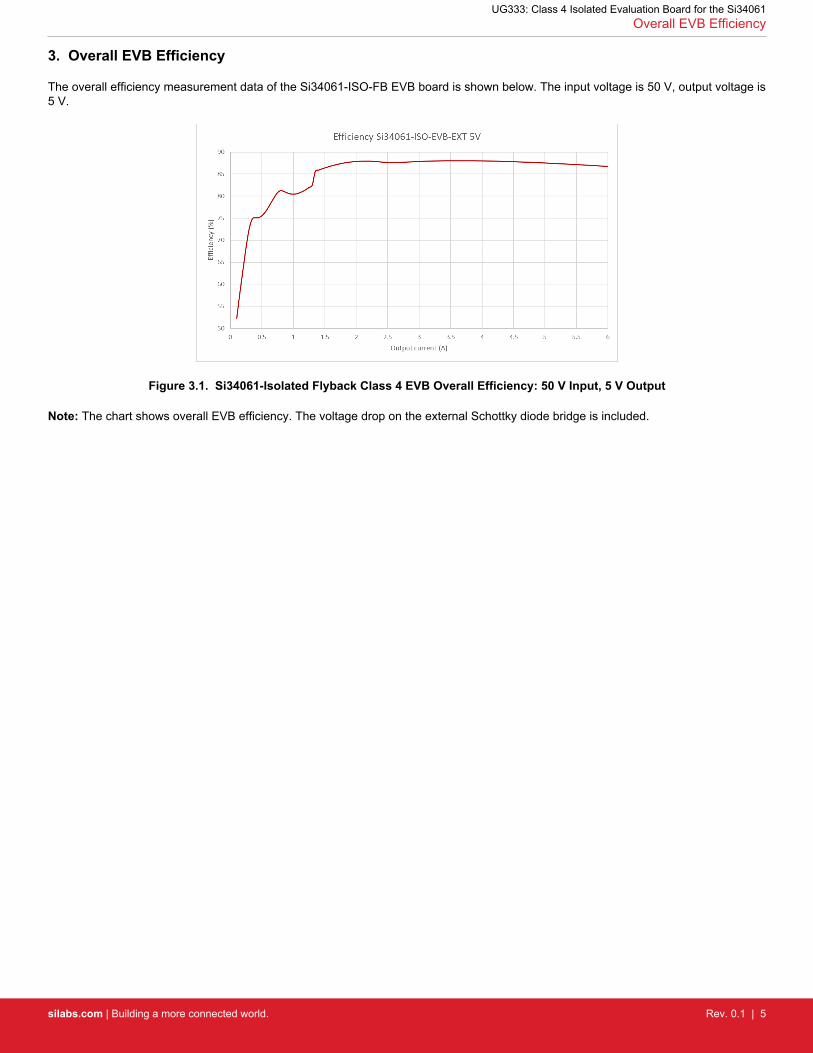
3. Overall EVB Efficiency
The overall efficiency measurement data of the Si34061-ISO-FB EVB board is shown below. The input voltage is 50 V, output voltage is5 V.
Figure 3.1. Si34061-Isolated Flyback Class 4 EVB Overall Efficiency: 50 V Input, 5 V Output
Note: The chart shows overall EVB efficiency. The voltage drop on the external Schottky diode bridge is included.
UG333: Class 4 Isolated Evaluation Board for the Si34061Overall EVB Efficiency
silabs.com | Building a more connected world. Rev. 0.1 | 5
4. SIFOS PoE Compatibility Test Results
The Si34061-ISO-FB EVB board has been successfully tested with PDA-300 Powered Device Analyzer from SIFOS Technologies. ThePDA-300 Powered Device Analyzer is a single-box comprehensive solution for testing IEEE 802.3at PoE Powered Devices (PDs).
UG333: Class 4 Isolated Evaluation Board for the Si34061SIFOS PoE Compatibility Test Results
silabs.com | Building a more connected world. Rev. 0.1 | 6
5. Feedback Loop Phase and Gain Measurement Results (Bode Plots)
The Si34061 device integrates a current mode controlled switching mode power supply controller circuit. Therefore, the application is aclosed-loop system. To guarantee a stable output voltage of a power supply and to reduce the influence of input supply voltage varia-tions and load changes on the output voltage, the feedback loop should be stable.
To verify the stability of the loop, the loop gain and loop phase shift has been measured.
-180
-90
0
90
180
-80
-60
-40
-20
0
20
40
60
80
100 1000 10000 100000
Frequency (Hz)
Loop
Gai
n (d
B)
Loop
Pha
se (°
)
Phase Margin
Gain Margin
Figure 5.1. Si34061-ISO-FB EVB Measured Loop-Gain and Phase Shift
Table 5.1. Measured Loop Gain and Phase Shift
Frequency Gain Phase
Cursor 1 (Phase Margin) 5.4 kHz 0 dB 54°
Cursor 2 (Gain Margin) 23 kHz –14 dB 0 °
UG333: Class 4 Isolated Evaluation Board for the Si34061Feedback Loop Phase and Gain Measurement Results (Bode Plots)
silabs.com | Building a more connected world. Rev. 0.1 | 7
6. Step Load Transient Measurement Results
The Si34061-ISO-FB EVB board's output has been tested with a step load function to verify the converters output dynamic response.
Step Load: From 1 A to 5 A Output Current Step Load: From 5 A to 1 A Output Current
Figure 6.1. Si34061-ISO-FB EVB PD Output Step Load Transient Test
UG333: Class 4 Isolated Evaluation Board for the Si34061Step Load Transient Measurement Results
silabs.com | Building a more connected world. Rev. 0.1 | 8
7. Output Voltage Ripple
The Si34061-ISO-FB C4 output voltage ripple has been measured in both no load and heavy load conditions.
Figure 7.1. Si34061-Isolated Flyback C4 EVB Output Voltage Ripple No Load (Left) and Heavy Load (Right) Conditions
UG333: Class 4 Isolated Evaluation Board for the Si34061Output Voltage Ripple
silabs.com | Building a more connected world. Rev. 0.1 | 9
8. Soft Start Protection
The Si34061 device has an integrated dynamic soft-start protection mechanism to avoid stressing the components by the sudden cur-rent or voltage changes associated with the initial charging of the output capacitors.
No-Load Soft-Start Heavy-Load Soft-Start
Figure 8.1. Si34061 Isolated Flyback C4 EVB Input Current and Output Voltage Soft-Start at Low Load (Left) and Heavy Load(Right) Conditions
UG333: Class 4 Isolated Evaluation Board for the Si34061Soft Start Protection
silabs.com | Building a more connected world. Rev. 0.1 | 10
9. Output Short Protection
The Si34061 device has an integrated output short protection mechanism, which protects the IC itself and the surrounding externalcomponents from overheating in the case of electrical short on the output.
Figure 9.1. Si34061-Isolated Flyback C4 EVB Output Voltage and Input Current when Output is Shorted
UG333: Class 4 Isolated Evaluation Board for the Si34061Output Short Protection
silabs.com | Building a more connected world. Rev. 0.1 | 11
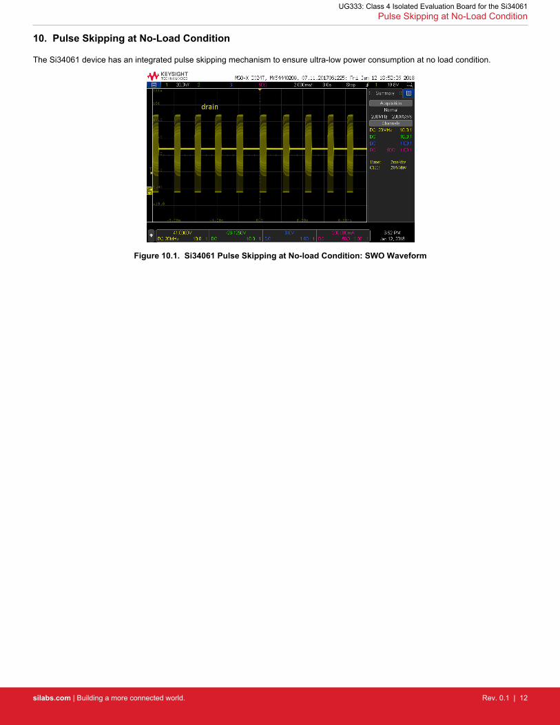
10. Pulse Skipping at No-Load Condition
The Si34061 device has an integrated pulse skipping mechanism to ensure ultra-low power consumption at no load condition.
Figure 10.1. Si34061 Pulse Skipping at No-load Condition: SWO Waveform
UG333: Class 4 Isolated Evaluation Board for the Si34061Pulse Skipping at No-Load Condition
silabs.com | Building a more connected world. Rev. 0.1 | 12
11. Adjustable EVB Current Limit
For additional safety, the Si34061 has an adjustable EVB current limit feature. The EVB current limit through the ISNS pin measuresthe voltage on RSENSE. When VRSENSE = -270 mV (referenced to Vss), the current limit circuit restarts the circuit to protect the applica-tion.
The EVB current limit for this Class 4 application can be calculated with the following formula:RSENSE = 0.3Ω
ILIMIT = 270mV0.3Ω = 900mA
Equation 1. EVB Current Limit
UG333: Class 4 Isolated Evaluation Board for the Si34061Adjustable EVB Current Limit
silabs.com | Building a more connected world. Rev. 0.1 | 13
12. Tunable Switching Frequency
The switching frequency of the oscillator is selected by choosing an external resistor (RFREQ) connected between the RFREQ andVPOS pins. The following figure will aid in choosing the RFREQ value to achieve the desired switching frequency.
Figure 12.1. Switching Frequency vs RFREQ
The selected switching frequency for this application is 220 kHz, which is achieved by setting the RFREQ resistor to 88.7 kΩ.
UG333: Class 4 Isolated Evaluation Board for the Si34061Tunable Switching Frequency
silabs.com | Building a more connected world. Rev. 0.1 | 14
13. Synchronous Rectification
The Si34061 device has synchronous gate driver (SYNCL) to drive the rectifier MOSFET. At low-load the converter works in discontinu-ous current mode (DCM); at heavy load, the converter runs in continuous current mode (CCM). At low-load the SWO voltage waveformhas a ringing waveform, which is typical for a DCM operation.
Figure 13.1. DC-DC Switch Drain and SYNCL Voltage Waveforms at Discontinuous Current Mode (DCM) (Left) and in Continu-ous Current Mode (CCM) (Right)
The device operates in non-synchronous mode at light load (IIN < 25 mA). As the input current increases, Si34061 automaticallychanges its switching operation from "Non-Synchronous" to "Synchronous". The dynamic operation adjustment maximizes overall pow-er efficiency.
UG333: Class 4 Isolated Evaluation Board for the Si34061Synchronous Rectification
silabs.com | Building a more connected world. Rev. 0.1 | 15
14. Maintain Power Signature
The Si34061 device integrates an MPS circuit which ensures connection with the PSE if the PD application current drops below PSEthreshold level.
There are two modes of MPS operation:• Automatic mode MPS (consumption-based)• User mode MPS
Automatic Mode MPS (Consumptions Based):
If nSLEEP is low at startup, MPS generation depends on chip current consumption:• MPS pulses are enabled below a certain level of total PD current consumption to ensure connection with the PSE• MPS pulses are disabled above a certain level of total PD current consumption not to degrade overall board efficiency
nSLEEP = low
IIN
Figure 14.1. Automatic MPS Mode, nSLEEP is Low; MPS is Enabled when PD Consumption is Low; MPS is Disabled when PDConsumption is Higher
User Mode MPS:
If nSLEEP is high at startup, MPS generation depends on nSLEEP.• if nSLEEP is high, MPS disabled (independently of the current consumption)• if nSLEEP is low, MPS enabled (independently of the current consumption)
nSLEEP = high
IIN
nSLEEP = low
At startup, nSLEEP was high
Figure 14.2. With nSLEEP High, MPS is Disabled (Left); with nSLEEP Low, MPS is Enabled (Right); MPSGeneration is Fully Controlled by the User
UG333: Class 4 Isolated Evaluation Board for the Si34061Maintain Power Signature
silabs.com | Building a more connected world. Rev. 0.1 | 16
15. Board Layout
Figure 15.1. Top Silkscreen
Figure 15.2. Top Layer
UG333: Class 4 Isolated Evaluation Board for the Si34061Board Layout
silabs.com | Building a more connected world. Rev. 0.1 | 17
Figure 15.3. Internal 1 (Layer 2)
Figure 15.4. Internal 2 (Layer 3)
Figure 15.5. Bottom Layer
UG333: Class 4 Isolated Evaluation Board for the Si34061Board Layout
silabs.com | Building a more connected world. Rev. 0.1 | 18
16. Bill of Materials
The following table is the BOM listing for the standard 5 V output evaluation board with option PoE Class 4.
1 ES1C D2 1.0 A 150 V Fast DO-214AC ES1C Diodes Inc.
1 1N4148W
D4 2 A 100 V Fast SOD123 1N4148W Diodes Inc
8 PDS5100 D5, D6, D7,D8, D9, D10,
D11, D12
5 A 100 V Schottky POWERDI-5 PDS5100H-13 Diodes Inc.
1 S1B D16 1.0 A 100 V Single DO-214AC S1B Fairchild
1 GREEN D17 30 mA 2.2 V SMT LED-0805-K LTST-C170GKT LITE_ON Inc.
1 PDS1040 D18 10 A 40 V Schottky POWERDI-5 PDS1040-13 Diodes Inc.
1 Header1x3
JP1 Header CONN-1X3 TSW-103-07-G-S Samtec
2 BND_POST
J1, J2 15 A BANA-NA
BANANA-JACK 101 Abbatron HHSmith
1 CONNTRBLK 2
J6 TERMBLK
CON1X2-1725656 1725656 Phoenix Con-tact
1 3.3 µH L2 1.5 A ±20% Unshiel-ded
IND-8400 84332C Murata
UG333: Class 4 Isolated Evaluation Board for the Si34061Bill of Materials
silabs.com | Building a more connected world. Rev. 0.1 | 19
Qty Value Ref Rating Volt-age
Tol Type PCB Footprint MfrPart Number
Mfr
1 0.16 µH L3 16 A ±20% Shiel-ded
IND-XAL5030-161ME
IND-XAL5030-161ME Coilcraft
4 330 Ω L4, L5, L6,L7
1500mA
SMT L0805 BLM21PG331SN1 MuRata
1 Si2328DS
Q1 1.5 A 100 V N-CHNL SOT23-GSD Si2328DS Vishay
3 1 kΩ R1, R2, R33 1/10 W ±1% Thick-Film
R0805 CR0805-10W-1001F Venkel
1 47 kΩ R3 1/10 W ±5% Thick-Film
R0805 CR0805-10W-473J Venkel
3 10 Ω R4, R6, R38 1/10 W ±1% Thick-Film
R0805 CR0805-10W-10R0F Venkel
1 88.7 kΩ R16 1/8 W ±1% Thick-Film
R0805 CRCW080588K7FKEA vishay
1 33.2 Ω R17 1/8 W ±1% Thick-Film
R0805 CRCW080533R2FKEA vishay
1 24.3 kΩ R20 1/8 W ±1% Thick-Film
R0805 CRCW080524K3FKEA vishay
1 3.24 kΩ R21 1/8 W ±1% Thick-Film
R0805 CRCW08053K24FKEA Vishay
1 2.2 kΩ R22 1/10 W ±5% Thick-Film
R0805 CR0805-10W-222J Venkel
1 36.5 kΩ R23 1/10 W ±1% Thick-Film
R0805 CR0805-10W-3652F Venkel
1 12.1 kΩ R24 1/10 W ±1% Thick-Film
R0805 CR0805-10W-1212F Venkel
3 0 Ω R25, R26,R37
2 A Thick-Film
R0805 CR0805-10W-000 Venkel
1 0.3 Ω R27 1/2 W ±1% Thick-Film
R1206 LRC-LR1206LF-01-R300-F
TT Electron-ics
1 0.1 Ω R28 1 W ±1% Thick-Film
R1206 ERJ-8BWFR100V Panasonic
1 200 kΩ R31 1/10 W ±1% Thick-Film
R0805 CR0805-10W-2003F Venkel
1 CX-9642 T1 25 W 37V-57 V
PoE+ CX-9642 Coilcraft
1 TGM-240NSLF
T2 1500 V TGM-240NSLF TGM-240NSLF Halo
1 RJ-45 U1 Recep-tacle
RJ45-SI-52004 SI-52003-F Bel
1 SiR422DP
U2 40 A 40 V N-CHNL POWER56 SiR422DP Vishay
1 Si34061 U3 120 V PD Si34061 SiLabs
1 Si7898DP
U4 4.8 A 150 V N-CHNL POWER56 Si7898DP Vishay
UG333: Class 4 Isolated Evaluation Board for the Si34061Bill of Materials
silabs.com | Building a more connected world. Rev. 0.1 | 20
Qty Value Ref Rating Volt-age
Tol Type PCB Footprint MfrPart Number
Mfr
1 VO618A-3X017T
U5 SO4N10.16P2.54-AKEC
VO618A-3X017T Vishay
1 TLV431 U6 SHUNT TLV431-DBZ TLV431BCDBZR TI
Not Installed Components
1 1 kΩ R13 1/10 W ±1% Thick-Film
R0805 CR0805-10W-1001F Venkel
UG333: Class 4 Isolated Evaluation Board for the Si34061Bill of Materials
silabs.com | Building a more connected world. Rev. 0.1 | 21
17. Appendix—Si34061ISOC4 Design and Layout Checklist
Although the EVB design is pre-configured as a Class 4 PD with 5 V output, the schematics and layouts can easily be adapted to meeta wide variety of common output voltages and power levels.
The complete EVB design databases for the standard 5 V/Class 4 configuration are located at www.silabs.com/PoE link. Silicon Labsstrongly recommends using these EVB schematics and layout files as a starting point to ensure robust performance and avoid commonmistakes in the schematic capture and PCB layout processes.
Below is a recommended design checklist that can assist in trouble-free development of robust PD designs.
Refer also to the Si34061 data sheet and AN1130 when using the following checklist.1. Design Planning checklist:
a. Determine if your design requires an isolated or non-isolated topology. For more information, see AN1130.b. Silicon Labs strongly recommends using the EVB schematics and layout files as a starting point as you begin integrating the
Si34061ISOC4 into your system design process.c. Determine your load’s power requirements (i.e., VOUT and IOUT consumed by the PD, including the typical expected transi-
ent surge conditions). In general, to achieve the highest overall efficiency performance of the Si34061-isolated Flyback,choose the highest output voltage option used in your PD and then post regulate to the lower supply rails, if necessary.
d. Based on your required PD power level, select the appropriate class resistor RCLASS value by referring to AN1130.2. General Design checklist:
a. ESD caps (C24–C31 in Figure 2.3 Si34061-Isolated Flyback EVB Schematic: 5 V, Class 4 PD on page 4) are strongly recom-mended for designs where system-level ESD (IEC6100-4-2) must provide >15 kV tolerance.
b. If your design uses an AUX supply, be sure to include a 3 Ω surge limiting resistor in series with the AUX supply for hot inser-tion. Refer to AN1130 when AUX supply is 48 V.
3. Layout Guidelines:a. Make sure VNEG pin of the Si34061 is connected to the backside of the QFN package with an adequate thermal plane, as
noted in the data sheet and AN1130.b. Keep the trace length from SWO to VSS as short as possible. Make all of the power (high current) traces as short, direct, and
thick as possible. It is a good practice on a standard PCB board to make the traces an absolute minimum of 15 mils (0.381mm) per ampere.
c. Usually, one standard via handles 200 mA of current. If the trace needs to conduct a significant amount of current from oneplane to the other, use multiple vias.
d. Keep the circular area of the loop from the Switcher FET output to the inductor or transformer and returning from the input filtercapacitors (C2–C4) to VSS as small a diameter as possible. Also, minimize the circular area of the loop from the output of theinductor or transformer to the Schottky diode and returning through the first stage output filter capacitor back to the inductor ortransformer as small as possible. If possible, keep the direction of current flow in these two loops the same.
e. Keep the high power traces as short as possible.f. Keep the feedback and loop stability components as far from the transformer/inductor and noisy power traces as possible.
g. If the outputs have a ground plane or positive output plane, do not connect the high current carrying components and the filtercapacitors through the plane. Connect them together, and then connect to the plane at a single point.
To help ensure first-pass success, contact our customer support by submitting a help ticket and uploading your schematics and layoutfiles for review.
UG333: Class 4 Isolated Evaluation Board for the Si34061Appendix—Si34061ISOC4 Design and Layout Checklist
silabs.com | Building a more connected world. Rev. 0.1 | 22
http://www.silabs.com
Silicon Laboratories Inc.400 West Cesar ChavezAustin, TX 78701USA
Smart. Connected. Energy-Friendly.
Productswww.silabs.com/products
Qualitywww.silabs.com/quality
Support and Communitycommunity.silabs.com
DisclaimerSilicon Labs intends to provide customers with the latest, accurate, and in-depth documentation of all peripherals and modules available for system and software implementers using or intending to use the Silicon Labs products. Characterization data, available modules and peripherals, memory sizes and memory addresses refer to each specific device, and "Typical" parameters provided can and do vary in different applications. Application examples described herein are for illustrative purposes only. Silicon Labs reserves the right to make changes without further notice and limitation to product information, specifications, and descriptions herein, and does not give warranties as to the accuracy or completeness of the included information. Silicon Labs shall have no liability for the consequences of use of the information supplied herein. This document does not imply or express copyright licenses granted hereunder to design or fabricate any integrated circuits. The products are not designed or authorized to be used within any Life Support System without the specific written consent of Silicon Labs. A "Life Support System" is any product or system intended to support or sustain life and/or health, which, if it fails, can be reasonably expected to result in significant personal injury or death. Silicon Labs products are not designed or authorized for military applications. Silicon Labs products shall under no circumstances be used in weapons of mass destruction including (but not limited to) nuclear, biological or chemical weapons, or missiles capable of delivering such weapons.
Trademark InformationSilicon Laboratories Inc.® , Silicon Laboratories®, Silicon Labs®, SiLabs® and the Silicon Labs logo®, Bluegiga®, Bluegiga Logo®, Clockbuilder®, CMEMS®, DSPLL®, EFM®, EFM32®, EFR, Ember®, Energy Micro, Energy Micro logo and combinations thereof, "the world’s most energy friendly microcontrollers", Ember®, EZLink®, EZRadio®, EZRadioPRO®, Gecko®, ISOmodem®, Micrium, Precision32®, ProSLIC®, Simplicity Studio®, SiPHY®, Telegesis, the Telegesis Logo®, USBXpress®, Zentri and others are trademarks or registered trademarks of Silicon Labs. ARM, CORTEX, Cortex-M3 and THUMB are trademarks or registered trademarks of ARM Holdings. Keil is a registered trademark of ARM Limited. All other products or brand names mentioned herein are trademarks of their respective holders.