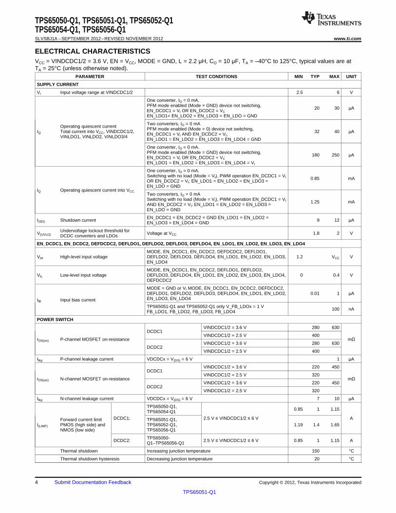
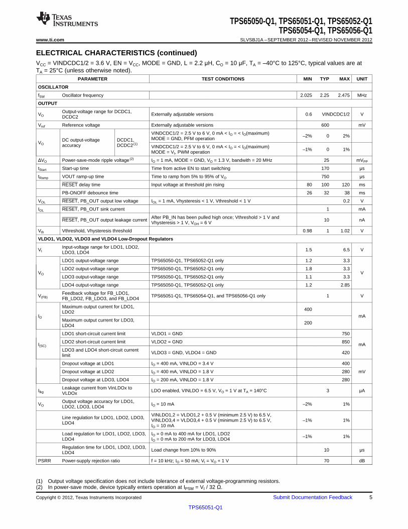
www.ti.com SLVSBJ1A –SEPTEMBER 2012–REVISED NOVEMBER 2012
6-CHANNEL POWER MGMT IC WITH TWO STEP-DOWN CONVERTERSAND 4 LOW-INPUT-VOLTAGE LDOs
, TPS65051-Q1
1FEATURES • Two General-Purpose 200-mA, High-PSRRLDOs
2• Qualified for Automotive Applications• VI Range for LDOs from 1.5 V to 6.5 V• AEC-Q100 Qualified With the Following• Digital Voltage Selection for the LDOsResults:• Available in a 4-mm × 4-mm 32-Pin QFN– Device Temperature Grade 1: –40°C to
• Up To 95% Efficiency DESCRIPTION• Output Current for DC-DC Converters: The TPS6505x-Q1 devices are integrated power-
– TPS65050-Q1: 2 × 0.6 A management ICs for applications powered by one Li-Ion or Li-Polymer cell, which require multiple power– TPS65051-Q1: DCDC1 = 1 A; DCDC2 = 0.6 Arails. The TPS6505x-Q1 provides two efficient, 2.25-– TPS65052-Q1: DCDC1 = 1 A; DCDC2 = 0.6 A MHz step-down converters targeted at providing the
– TPS65054-Q1: 2 × 0.6 A core voltage and I/O voltage in a processor-basedsystem. Both step-down converters enter a low-power– TPS65056-Q1: DCDC1 = 1 A; DCDC2 = 0.6 Amode at light load for maximum efficiency across the• Output Voltages for DC-DC Converters:widest possible range of load currents.
– TPS65050-Q1: Externally AdjustableFor low-noise applications, the user can force the– TPS65051-Q1: Externally Adjustable devices into fixed-frequency PWM mode by pulling
– TPS65052-Q1: DCDC1 = Fixed at 3.3 V; the MODE pin high. Operating in the shutdown modeDCDC2 = 1 V or 1.3 V for Samsung reduces the current consumption to less than 1 μA.
The devices allow the use of small inductors andApplication Processorscapacitors to achieve a small solution size. The– TPS65054-Q1: DCDC1 = ExternallyTPS6505x-Q1 provides an output current of up to 1 AAdjustable; DCDC2 = 1.3 V or 1.05 V foron each dc-dc converter. The TPS6505x-Q1 alsoOMAP™1710 Processor integrates two 400-mA LDO and two 200-mA LDO
– TPS65056-Q1: DCDC1 = Fixed at 3.3 V; voltage regulators, which one can turn on or off usingDCDC2 = 1 V or 1.3 V for Samsung separate enable pins on each LDO. Each LDOApplication Processors operates with an input voltage range between 1.5 V
and 6.5 V, allowing their supply to be from one of the• VI Range for DC-DC Convertersstep-down converters or directly from the mainFrom 2.5 V to 6 Vbattery.
• 2.25-MHz Fixed-Frequency OperationFour digital input pins set the output voltage of the• Power-Save Mode at Light Load CurrentLDOs from a set of 16 different combinations for
• 180° Out-of-Phase Operation LDO1 to LDO4 on TPS65050-Q1 and TPS65052-Q1.In TPS65051-Q1, TPS65054-Q1, and TPS65056-Q1,• Output-Voltage Accuracy in PWM Mode ±1%the LDO voltages are adjustable using external• Low-Ripple PFM Moderesistor dividers.
• Total Typical 32-μA Quiescent Current for BothThe TPS6505x-Q1 devices come in a small 32-pinDC-DC Convertersleadless package (4-mm × 4-mm QFN) with a 0.4-
• 100% Duty Cycle for Lowest Dropout mm pitch.• Two General-Purpose 400-mA, High-PSRR
LDOs1
Please be aware that an important notice concerning availability, standard warranty, and use in critical applications ofTexas Instruments semiconductor products and disclaimers thereto appears at the end of this data sheet.
TPS65050-Q1, TPS65051-Q1, TPS65052-Q1TPS65054-Q1, TPS65056-Q1SLVSBJ1A –SEPTEMBER 2012–REVISED NOVEMBER 2012 www.ti.com
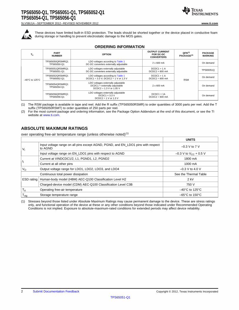
These devices have limited built-in ESD protection. The leads should be shorted together or the device placed in conductive foamduring storage or handling to prevent electrostatic damage to the MOS gates.
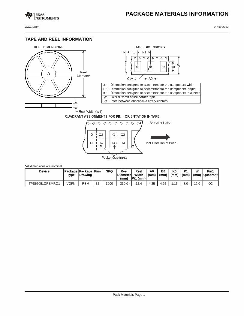
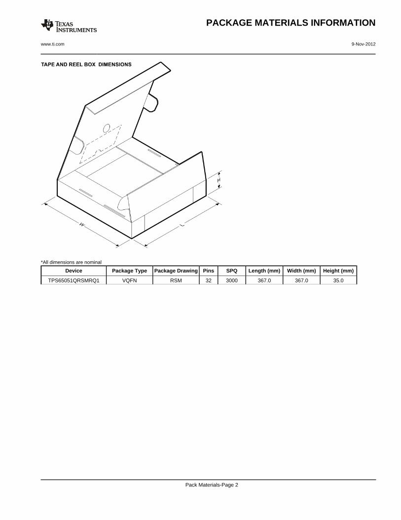
(1) The RSM package is available in tape and reel. Add the R suffix (TPS65050RSMR) to order quantities of 3000 parts per reel. Add the Tsuffix (TPS65050RSMT) to order quantities of 250 parts per reel.
(2) For the most current package and ordering information, see the Package Option Addendum at the end of this document, or see the TIwebsite at www.ti.com.
ABSOLUTE MAXIMUM RATINGSover operating free-air temperature range (unless otherwise noted) (1)
UNITS
Input voltage range on all pins except AGND, PGND, and EN_LDO1 pins with respect –0.3 V to 7 Vto AGNDVI
Input voltage range on EN_LDO1 pins with respect to AGND –0.3 V to VCC + 0.5 V
Current at VINDCDC1/2, L1, PGND1, L2, PGND2 1800 mAII
Current at all other pins 1000 mA
VO Output voltage range for LDO1, LDO2, LDO3, and LDO4 –0.3 V to 4.0 V
Continuous total power dissipation See the Thermal Table
Charged-device model (CDM) AEC-Q100 Classification Level C3B 750 V
TA Operating free-air temperature –40°C to 125°C
Tstg Storage temperature range –65°C to 150°C
(1) Stresses beyond those listed under Absolute Maximum Ratings may cause permanent damage to the device. These are stress ratingsonly, and functional operation of the device at these or any other conditions beyond those indicated under Recommended OperatingConditions is not implied. Exposure to absolute-maximum-rated conditions for extended periods may affect device reliability.
www.ti.com SLVSBJ1A –SEPTEMBER 2012–REVISED NOVEMBER 2012
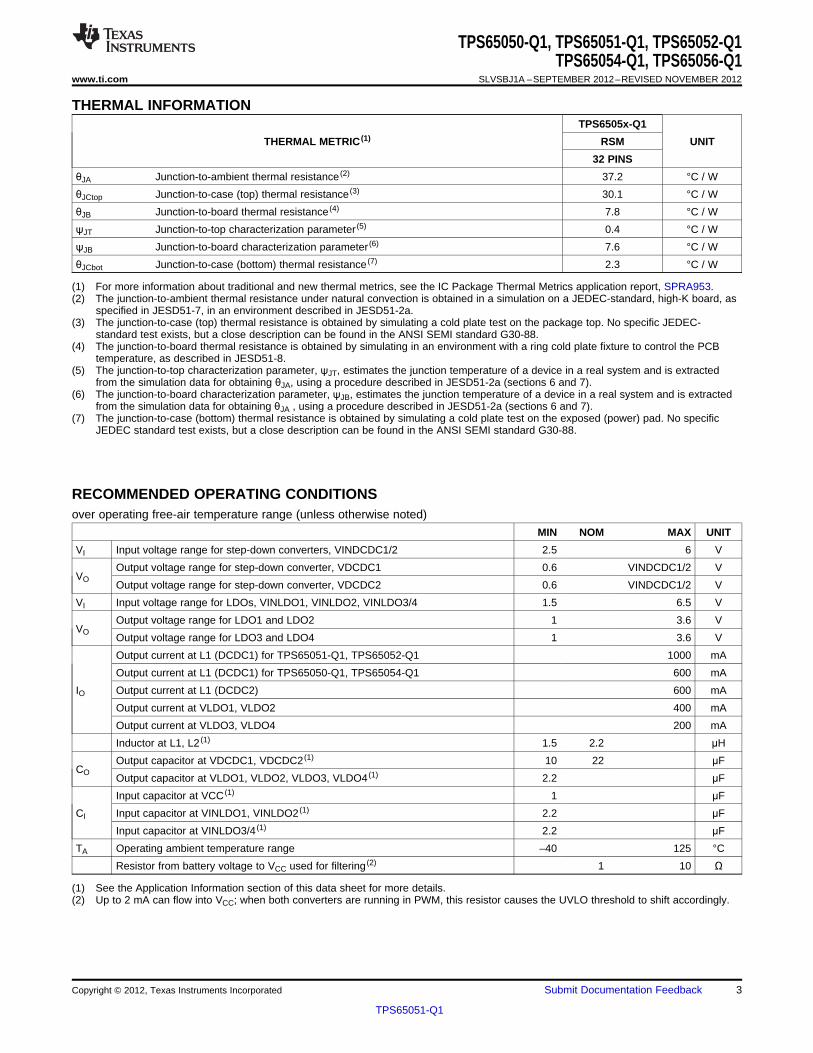
THERMAL INFORMATIONTPS6505x-Q1
THERMAL METRIC (1) RSM UNIT
32 PINS
θJA Junction-to-ambient thermal resistance (2) 37.2 °C / W
θJCtop Junction-to-case (top) thermal resistance (3) 30.1 °C / W
θJB Junction-to-board thermal resistance (4) 7.8 °C / W
ψJT Junction-to-top characterization parameter (5) 0.4 °C / W
ψJB Junction-to-board characterization parameter (6) 7.6 °C / W
θJCbot Junction-to-case (bottom) thermal resistance (7) 2.3 °C / W
(1) For more information about traditional and new thermal metrics, see the IC Package Thermal Metrics application report, SPRA953.(2) The junction-to-ambient thermal resistance under natural convection is obtained in a simulation on a JEDEC-standard, high-K board, as
specified in JESD51-7, in an environment described in JESD51-2a.(3) The junction-to-case (top) thermal resistance is obtained by simulating a cold plate test on the package top. No specific JEDEC-
standard test exists, but a close description can be found in the ANSI SEMI standard G30-88.(4) The junction-to-board thermal resistance is obtained by simulating in an environment with a ring cold plate fixture to control the PCB
temperature, as described in JESD51-8.(5) The junction-to-top characterization parameter, ψJT, estimates the junction temperature of a device in a real system and is extracted
from the simulation data for obtaining θJA, using a procedure described in JESD51-2a (sections 6 and 7).(6) The junction-to-board characterization parameter, ψJB, estimates the junction temperature of a device in a real system and is extracted
from the simulation data for obtaining θJA , using a procedure described in JESD51-2a (sections 6 and 7).(7) The junction-to-case (bottom) thermal resistance is obtained by simulating a cold plate test on the exposed (power) pad. No specific
JEDEC standard test exists, but a close description can be found in the ANSI SEMI standard G30-88.Spacer
spacer
RECOMMENDED OPERATING CONDITIONSover operating free-air temperature range (unless otherwise noted)
MIN NOM MAX UNIT
VI Input voltage range for step-down converters, VINDCDC1/2 2.5 6 V
Output voltage range for step-down converter, VDCDC1 0.6 VINDCDC1/2 VVO
Output voltage range for step-down converter, VDCDC2 0.6 VINDCDC1/2 V
VI Input voltage range for LDOs, VINLDO1, VINLDO2, VINLDO3/4 1.5 6.5 V
Output voltage range for LDO1 and LDO2 1 3.6 VVO
Output voltage range for LDO3 and LDO4 1 3.6 V
Output current at L1 (DCDC1) for TPS65051-Q1, TPS65052-Q1 1000 mA
Output current at L1 (DCDC1) for TPS65050-Q1, TPS65054-Q1 600 mA
IO Output current at L1 (DCDC2) 600 mA
Output current at VLDO1, VLDO2 400 mA
Output current at VLDO3, VLDO4 200 mA
Inductor at L1, L2 (1) 1.5 2.2 μH
Output capacitor at VDCDC1, VDCDC2 (1) 10 22 μFCO
Output capacitor at VLDO1, VLDO2, VLDO3, VLDO4 (1) 2.2 μF
Input capacitor at VCC (1) 1 μF
CI Input capacitor at VINLDO1, VINLDO2 (1) 2.2 μF
Input capacitor at VINLDO3/4 (1) 2.2 μF
TA Operating ambient temperature range –40 125 °C
Resistor from battery voltage to VCC used for filtering (2) 1 10 Ω
(1) See the Application Information section of this data sheet for more details.(2) Up to 2 mA can flow into VCC; when both converters are running in PWM, this resistor causes the UVLO threshold to shift accordingly.
tStart Start-up time Time from active EN to start switching 170 μs
tRamp VOUT ramp-up time Time to ramp from 5% to 95% of VO 750 μs
RESET delay time Input voltage at threshold pin rising 80 100 120 ms
PB-ONOFF debounce time 26 32 38 ms
VOL RESET, PB_OUT output low voltage IOL = 1 mA, Vhysteresis < 1 V, Vthreshold < 1 V 0.2 V
IOL RESET, PB_OUT sink current 1 mA
After PB_IN has been pulled high once; Vthreshold > 1 V andRESET, PB_OUT output leakage current 10 nAVhysteresis > 1 V, VOH = 6 V
Vth Vthreshold, Vhysteresis threshold 0.98 1 1.02 V
VLDO1, VLDO2, VLDO3 and VLDO4 Low-Dropout Regulators
Input-voltage range for LDO1, LDO2,VI 1.5 6.5 VLDO3, LDO4
LDO1 output-voltage range TPS65050-Q1, TPS65052-Q1 only 1.2 3.3
LDO2 output-voltage range TPS65050-Q1, TPS65052-Q1 only 1.8 3.3VO V
LDO3 output-voltage range TPS65050-Q1, TPS65052-Q1 only 1.1 3.3
LDO4 output-voltage range TPS65050-Q1, TPS65052-Q1 only 1.2 2.85
Feedback voltage for FB_LDO1,V(FB) TPS65051-Q1, TPS65054-Q1, and TPS65056-Q1 only 1 VFB_LDO2, FB_LDO3, and FB_LDO4
Maximum output current for LDO1, 400LDO2IO mA
Maximum output current for LDO3, 200LDO4
LDO1 short-circuit current limit VLDO1 = GND 750
LDO2 short-circuit current limit VLDO2 = GND 850I(SC) mALDO3 and LDO4 short-circuit current VLDO3 = GND, VLDO4 = GND 420limit
Dropout voltage at LDO1 IO = 400 mA, VINLDO = 3.4 V 400
Dropout voltage at LDO2 IO = 400 mA, VINLDO = 1.8 V 280 mV
Dropout voltage at LDO3, LDO4 IO = 200 mA, VINLDO = 1.8 V 280
Leakage current from VinLDOx toIlkg LDO enabled, VINLDO = 6.5 V, VO = 1 V at TA = 140°C 3 μAVLDOx
Output voltage accuracy for LDO1,VO IO = 10 mA –2% 1%LDO2, LDO3, LDO4
VINLDO1,2 = VLDO1,2 + 0.5 V (minimum 2.5 V) to 6.5 V,Line regulation for LDO1, LDO2, LDO3, VINLDO3,4 = VLDO3,4 + 0.5 V (minimum 2.5 V) to 6.5 V, –1% 1%LDO4 IO = 10 mA
Load regulation for LDO1, LDO2, LDO3, IO = 0 mA to 400 mA for LDO1, LDO2 –1% 1%LDO4 IO = 0 mA to 200 mA for LDO3, LDO4
Regulation time for LDO1, LDO2, LDO3, Load change from 10% to 90% 10 μsLDO4
PSRR Power-supply rejection ratio f = 10 kHz; IO = 50 mA; VI = VO + 1 V 70 dB
(1) Output voltage specification does not include tolerance of external voltage-programming resistors.(2) In power-save mode, device typically enters operation at IPSM = VI / 32 Ω.
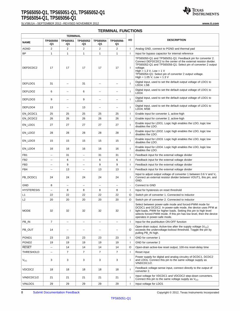
AGND 2 2 2 2 2 I Analog GND, connect to PGND and thermal pad
BP 1 1 1 1 1 I Input for bypass capacitor for internal reference
TPS65050-Q1 and TPS65051-Q1: Feedback pin for converter 2.Connect DEFDCDC2 to the center of the external resistor divider.TPS65052-Q1 and TPS65056-Q1: Select pin of converter 2 output
DEFDCDC2 17 17 17 17 17 I voltage.High = 1.3 V, Low = 1 VTPS65054-Q1: Select pin of converter 2 output voltage.High = 1.05 V, Low = 1.3 V
Digital input, used to set the default output voltage of LDO1 toDEFLDO1 31 -- 31 -- -- I LDO4; LSB
Digital input, used to set the default output voltage of LDO1 toDEFLDO2 6 -- 6 -- -- I LDO4
Digital input, used to set the default output voltage of LDO1 toDEFLDO3 9 -- 9 -- -- I LDO4
Digital input, used to set the default output voltage of LDO1 toDEFLDO4 13 -- 13 -- -- I LDO4; MSB
EN_DCDC1 25 25 25 25 25 I Enable input for converter 1, active-high
EN_DCDC2 26 26 26 26 26 I Enable input for converter 2, active-high
Enable input for LDO1. Logic high enables the LDO, logic lowEN_LDO1 27 27 27 27 27 I disables the LDO.
Enable input for LDO2. Logic high enables the LDO, logic lowEN_LDO2 28 28 28 28 28 I disables the LDO.
Enable input for LDO3. Logic high enables the LDO, logic lowEN_LDO3 15 15 15 15 15 I disables the LDO.
Enable input for LDO4. Logic high enables the LDO, logic lowEN_LDO4 16 16 16 16 16 I disables the LDO.
FB1 -- 31 -- 31 31 I Feedback input for the external voltage divider
FB2 -- 6 -- 6 6 I Feedback input for the external voltage divider
FB3 -- 9 -- 9 9 I Feedback input for the external voltage divider
FB4 -- 13 -- 13 13 I Feedback input for the external voltage divider
Input to adjust output voltage of converter 1 between 0.6 V and VI.FB_DCDC1 24 24 24 24 24 I Connect an external resistor divider between VOUT1, this pin, and
GND.
GND 8 -- -- -- -- - Connect to GND
HYSTERESIS -- 8 8 8 8 I Input for hysteresis on reset threshold
L1 22 22 22 22 22 O Switch pin of converter 1. Connected to inductor
L2 20 20 20 20 20 O Switch pin of converter 2. Connected to inductor
Select between power-safe mode and forced-PWM mode forDCDC1 and DCDC2. In power-safe mode, the device uses PFM at
MODE 32 32 32 32 32 I light loads, PWM for higher loads. Setting this pin to high levelselects forced-PWM mode. If this pin has low level, then the deviceoperates in power-safe mode.
PB_IN 7 -- -- -- -- I Input for the pushbutton ON-OFF function
Open-drain output. Active-low after the supply voltage (VCC)PB_OUT 14 -- -- -- -- O exceeds the undervoltage-lockout threshold. Toggle the pin by
pulling PB_IN high.
PGND1 23 23 23 23 23 I GND for converter 1
PGND2 19 19 19 19 19 I GND for converter 2
RESET -- 14 14 14 14 O Open-drain active-low reset output, 100-ms reset-delay time
THRESHOLD -- 7 7 7 7 I Reset input
Power supply for digital and analog circuitry of DCDC1, DCDC2VCC 3 3 3 3 3 I and LDOs. Connect this pin to the same voltage supply as
VINDCDC1/2.
Feedback voltage-sense input, connect directly to the output ofVDCDC2 18 18 18 18 18 I converter 2.
Input voltage for VDCDC1 and VDCDC2 step-down converters.VINDCDC1/2 21 21 21 21 21 I Connect this pin to the same voltage supply as VCC.
TPS65050-Q1, TPS65051-Q1, TPS65052-Q1TPS65054-Q1, TPS65056-Q1SLVSBJ1A –SEPTEMBER 2012–REVISED NOVEMBER 2012 www.ti.com
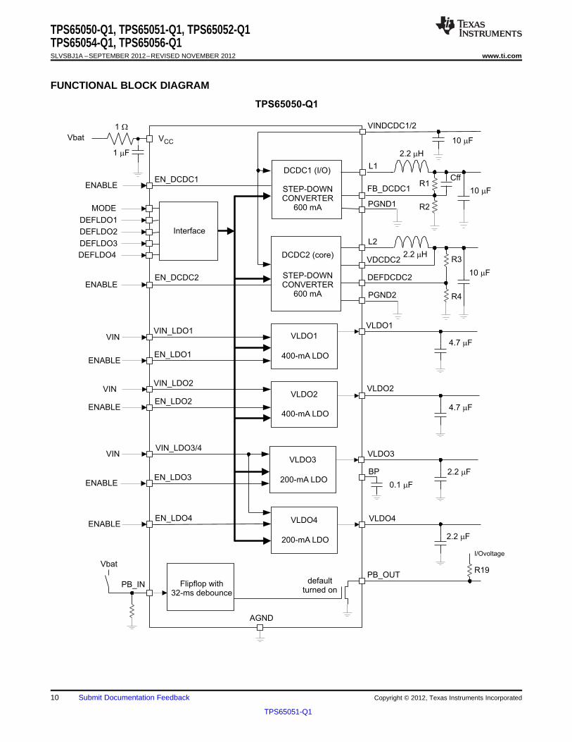
DETAILED DESCRIPTION
Operation
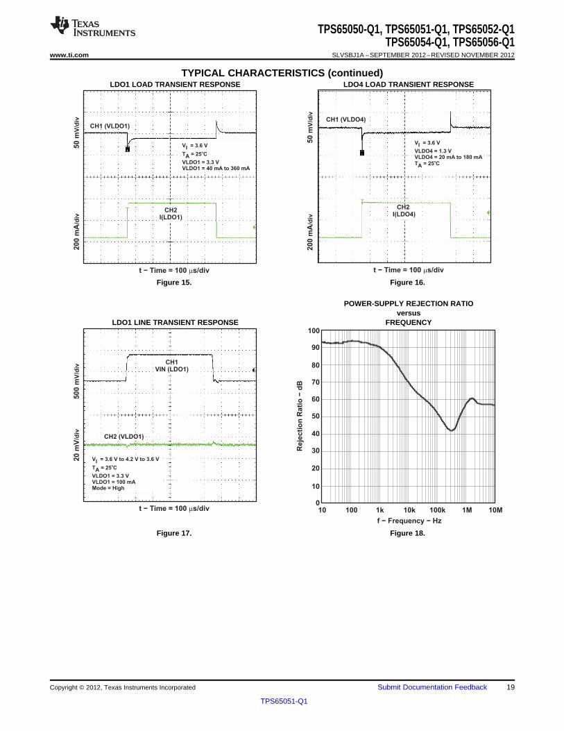
The TPS6505x-Q1 devices each include two synchronous step-down converters. The converters operate with2.25-MHz (typical) fixed-frequency pulse-width modulation (PWM) at moderate to heavy load currents. At lightload currents, the converters automatically enter power-save mode and operate with PFM (pulse-frequencymodulation).
During PWM operation, the converters use a unique fast-response voltage-mode controller scheme with inputvoltage feed-forward to achieve good line and load regulation, allowing the use of small ceramic input and outputcapacitors. At the beginning of each clock cycle initiated by the clock signal, the P-channel MOSFET switch turnson, the inductor current ramps up until the current comparator trips, and the control logic turns off the switch. Thecurrent-limit comparator turns off the switch if the current exceeds the limit of the P-channel switch. After theadaptive dead time, which prevents shoot-through current, the N-channel MOSFET rectifier turns on, and theinductor current ramps down. The clock signal turning off the N-channel rectifier and turning on the on the P-channel switch initiates the next cycle.
The two dc-dc converters operate synchronized to each other, with converter 1 as the master. A 180° phase shiftbetween converter 1 and converter 2 decreases the input rms current, allowing the use of smaller inputcapacitors.
DCDC1 Converter
An external resistor divider connected to FB_DCDC1 pin for TPS65050-Q1, TPS65051-Q1, and TPS65054-Q1sets the converter 1 output voltage. For TPS65052-Q1, with its output voltage fixed to 3.3 V, connect this pindirectly to the output. See the Application Information section for more details. The maximum output current onDCDC1 is 600 mA for TPS65050-Q1 and TPS65054-Q1. For TPS65051-Q1, TPS65052-Q1, and TPS65056-Q1,the maximum output current is 1 A.
DCDC2 Converter
Connect he VDCDC2 pin directly to the DCDC2 converter output voltage. The DEFDCDC2 pin selects theDCDC2 converter output voltage.
TPS65050-Q1 and TPS65051-Q1: An external resistor divider sets the output voltage. Connect the DEFDCDC2pin to the external resistor divider.
TPS65052-Q1, TPS65054-Q1, and TPS65056-Q1: Connect the DEFDCDC2 pin either to GND, or to VCC. Theconverter 2 output voltage defaults to:
www.ti.com SLVSBJ1A –SEPTEMBER 2012–REVISED NOVEMBER 2012
Power-Save Mode
Setting the MODE pin to 0 enables the power-save mode. If the load current decreases, the converters enter thepower-save mode of operation automatically. During power-save mode, the converters operate with reducedswitching frequency in PFM mode, and with a minimum quiescent current to maintain high efficiency. Theconverters position the output voltage 1% above the nominal output voltage. This voltage-positioning featureminimizes voltage drops caused by a sudden load step.
To optimize the converter efficiency at light load, the TPS6505x-Q1 monitors average current. If in PWM mode,the inductor current remains below a certain threshold, then the device enters power-save mode. Use Equation 1to calculate the typical threshold:
A. Average output current threshold to enter PFM mode. (1)
B. Average output current threshold to leave PFM mode. (2)
During power-save mode, a comparator monitors the output voltage. As the output voltage falls below the skip-comparator (skip comp) threshold, the P-channel switch turns on, and the converter effectively delivers aconstant current. If the load is below the delivered current, the output voltage rises until it crosses the skip compthreshold again; then all switching activity ceases, reducing the quiescent current to a minimum until the outputvoltage has dropped below the threshold. If the load current is greater than the delivered current, the outputvoltage falls until it crosses the skip-comparator-low (skip comp low) threshold set to 1% below nominal VO; thenthe device exits power-save mode, and the converter returns to the PWM mode.
These control methods reduce the quiescent current to 12 μA per converter and the switching frequency to aminimum, achieving the highest converter efficiency. The PFM mode operates with low output-voltage ripple. Theripple depends on the comparator delay and the size of the output capacitor; increasing capacitor valuedecreases the output ripple voltage.
Disable the power-save mode by driving the MODE pin high. In forced-PWM mode, both converters operate withfixed-frequency PWM mode regardless of the load.
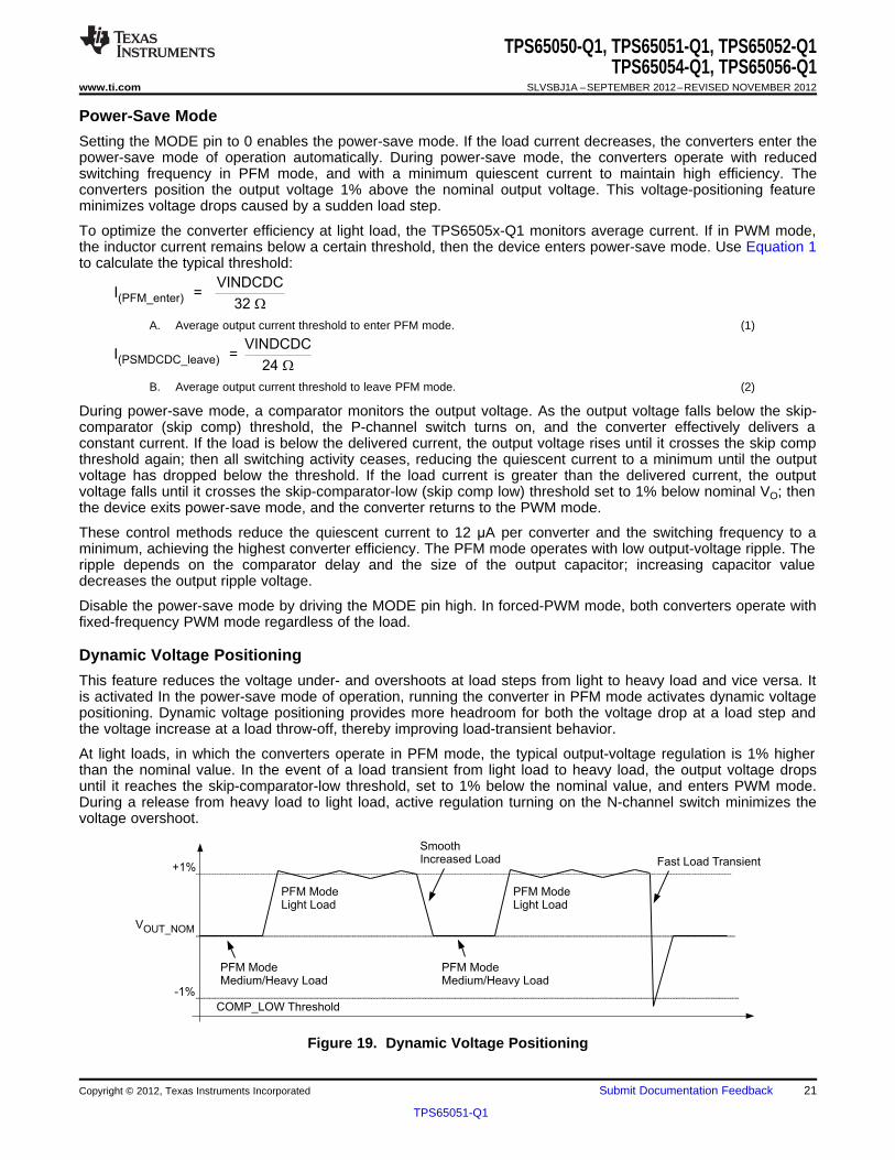
Dynamic Voltage Positioning
This feature reduces the voltage under- and overshoots at load steps from light to heavy load and vice versa. Itis activated In the power-save mode of operation, running the converter in PFM mode activates dynamic voltagepositioning. Dynamic voltage positioning provides more headroom for both the voltage drop at a load step andthe voltage increase at a load throw-off, thereby improving load-transient behavior.
At light loads, in which the converters operate in PFM mode, the typical output-voltage regulation is 1% higherthan the nominal value. In the event of a load transient from light load to heavy load, the output voltage dropsuntil it reaches the skip-comparator-low threshold, set to 1% below the nominal value, and enters PWM mode.During a release from heavy load to light load, active regulation turning on the N-channel switch minimizes thevoltage overshoot.
V (min) =I V (max) + I (max) x (r (max) + R )O O DS(on) L
95%
EN
5%
VOUT
tStart
tRAMP
TPS65050-Q1, TPS65051-Q1, TPS65052-Q1TPS65054-Q1, TPS65056-Q1SLVSBJ1A –SEPTEMBER 2012–REVISED NOVEMBER 2012 www.ti.com
Soft Start
The two converters have an internal soft-start circuit that limits the inrush current during start-up. During softstart, control of the output-voltage ramp-up is as shown in Figure 20.
Figure 20. Soft Start
100% Duty-Cycle Low-Dropout Operation
The converters offer a low input-to-output voltage difference while still maintaining operation with the use of the100% duty-cycle mode. In this mode, the P-channel switch is constantly on. This operational mode is useful inbattery-powered applications to achieve longest operation time by taking full advantage of the whole batteryvoltage range, (that is, the minimum input voltage to maintain regulation depends on the load current and outputvoltage) and can be calculated as:
(3)
with:• IO max = maximum output current plus inductor ripple current• rDS(on) max = maximum P-channel switch rDS(on)
• RL = dc resistance of the inductor• VO (max) = nominal output voltage plus maximum output-voltage tolerance
Undervoltage Lockout
The undervoltage-lockout circuit prevents the device from malfunctioning at low input voltages and fromexcessive discharge of the battery, and disables all internal circuitry. The undervoltage-lockout threshold, sensedat the VCC pin, is typically 1.8 V, maximum 2 V.
Mode Selection
The MODE pin allows mode selection between forced PWM mode and power-save mode for both converters.Connecting this pin to GND enables the automatic PWM and power-save mode of operation. The convertersoperate in fixed-frequency PWM mode at moderate-to-heavy loads and in the PFM mode during light loads,maintaining high efficiency over a wide load-current range.
www.ti.com SLVSBJ1A –SEPTEMBER 2012–REVISED NOVEMBER 2012
Pulling the MODE pin high forces both converters to operate constantly in the PWM mode even at light loadcurrents. The advantage is the converters operate with a fixed frequency that allows simple filtering of theswitching frequency for noise-sensitive applications. In this mode, the efficiency is lower compared to the power-save mode during light loads. For additional flexibility, it is possible to switch from power-save mode to forced-PWM mode during operation. This allows efficient power management by adjusting the operation of theconverters to the specific system requirements.
Enable
To start up each converter independently, the device has a separate enable pin for each dc-dc converter and foreach LDO. If EN_DCDC1, EN_DCDC2, EN_LDO1, EN_LDO2, EN_LDO3, or EN_LDO4 is set to high, thecorresponding converter starts up with soft start as previously described.
Pulling the enable pin low forces the device into shutdown, with a shutdown quiescent current as defined in theelectrical characteristics. In this mode, the P- and N-Channel MOSFETs turn off, and the entire internal controlcircuitry switches off. If disabled, internal 350-Ω resistors pull the outputs of the LDOs low, actively dischargingthe output capacitor. Proper operation requires termination of the enable pins. Do not leave them unconnected.
RESET
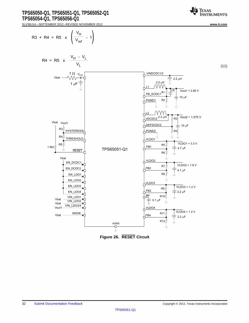
The TPS65051-Q1, TPS65052-Q1, TPS65054-Q1, and TPS65056-Q1 contain circuitry that can generate a resetpulse for a processor with a 100-ms delay time. The device senses the input voltage for a comparator at theTHRESHOLD pin. When the voltage exceeds the threshold, the output goes high with a 100-ms delay time. Anexternal resistor connected to the HYSTERESIS input defines the hysteresis. This circuitry is functional as soonas the supply voltage at VCC exceeds the undervoltage-lockout threshold. The TPS6505x-Q1 has a shutdowncurrent (all dc-dc converters and LDOs are off) of 9 μA.
TPS65050-Q1, TPS65051-Q1, TPS65052-Q1TPS65054-Q1, TPS65056-Q1SLVSBJ1A –SEPTEMBER 2012–REVISED NOVEMBER 2012 www.ti.com
Push-Button ON-OFF (PB-ON-OFF)
The TPS65050-Q1 provides a PB-ON-OFF functionality instead of supervising a voltage with the threshold andhysteresis inputs. The device holds the output at PB_OUT low after application of voltage at VCC. Only afterpulling the input at PB_IN high once, the output driver at PB_OUT goes to its inactive state, driven high with itsexternal pullup resistor. Further low-high pulses at PB_IN toggle the status of the PB_OUT output. Connectingthe PB_OUT output to the enable input of the converters allows shutdown and start-up of the converters with asingle push on a button.
Figure 22. Push-Button Circuit
Short-Circuit Protection
All outputs are short-circuit protected with a maximum output current as defined in the Electrical Characteristics.
Thermal Shutdown
As soon as the junction temperature, TJ, exceeds 150°C (typically) for the dc-dc converters, the device goes intothermal shutdown. In this mode, the P- and N-channel MOSFETs turn off. The device continues its operationwhen the junction temperature falls below the thermal shutdown hysteresis again. A thermal shutdown for one ofthe dc-dc converters disables both converters simultaneously.
The thermal shutdown temperature for the LDOs is typically 140°C. Therefore, an LDO used to power anexternal voltage never heats up the chip high enough to turn off the dc-dc converters. If one LDO exceeds thethermal shutdown temperature, all LDOs turn off simultaneously.
www.ti.com SLVSBJ1A –SEPTEMBER 2012–REVISED NOVEMBER 2012
Low Dropout Voltage Regulators
The design of the low-dropout voltage regulators allows them to operate well with small ceramic input and outputcapacitors. They operate with input voltages down to 1.5 V. The LDOs offer a maximum dropout voltage of280 mV at rated output current. Each LDO supports a current-limit feature. The EN_LDO1, ENLDO2, EN_LDO3,and EN_LDO4 pins enable the LDOs. In TPS65050-Q1 and TPS65052-Q1, the the use of four pins sets theoutput voltage of the LDOs. Connect the DEFLDO1 to DEFLDO4 pins either to GND or Vbat (VCC) to define a setof output voltages for LDO1 to LDO4 according to Table 1. Connecting the DEFLDOx pins to a voltage differentfrom GND or VCC causes increased leakage current into VCC. In TPS65051-Q1 and TPS65054-Q1, the use ofexternal resistor dividers sets the output voltage of the LDOs .
TPS65050-Q1 and TPS65052-Q1 default voltage options are adjustable with DEFLDO4…DEFLDO1 according toTable 1.
TPS65050-Q1, TPS65051-Q1, TPS65052-Q1TPS65054-Q1, TPS65056-Q1SLVSBJ1A –SEPTEMBER 2012–REVISED NOVEMBER 2012 www.ti.com
APPLICATION INFORMATION
Output-Voltage Setting
Converter 1 (DCDC1)
An external resistor network can set the output voltage of converter 1. Calculate the output voltage usingEquation 4,
(4)
with an internal reference voltage Vref, 0.6 V.
TI recommends setting the total resistance of R1 + R2 to less than 1 MΩ. The resistor network connects to theinput of the feedback amplifier, therefore requiring a small feed-forward capacitor in parallel with R1. A typicalvalue of 47 pF is sufficient.
Converter 2 (DCDC2)
Select the output voltage of converter 2 as follows:• Adjustable output voltage defined with external resistor network on pin DEFDCDC2. This option is available
for TPS65050-Q1 and TPS65051-Q1.• Two default fixed output voltages selectable by pin DEFDCDC2, see Table 2. This option is available for
TPS65052-Q1, TPS65054-Q1, and TPS65056-Q1.
Table 2. Default Fixed Output Voltages
Converter 2 DEFDCDC2 = Low DEFDCDC2 = High
TPS65050-Q1 — —
TPS65051-Q1 — —
TPS65052-Q1 1 V 1.3 V
TPS65054-Q1 1.3 V 1.05 V
TPS65056-Q1 1 V 1.3 V
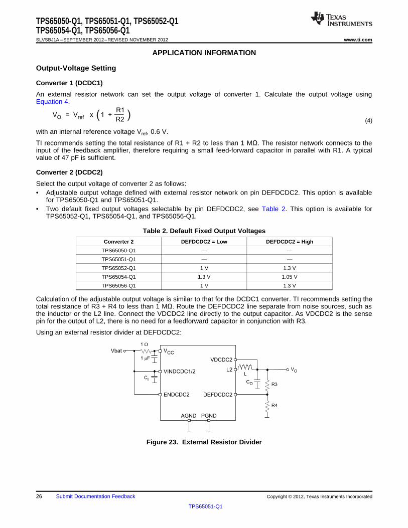
Calculation of the adjustable output voltage is similar to that for the DCDC1 converter. TI recommends setting thetotal resistance of R3 + R4 to less than 1 MΩ. Route the DEFDCDC2 line separate from noise sources, such asthe inductor or the L2 line. Connect the VDCDC2 line directly to the output capacitor. As VDCDC2 is the sensepin for the output of L2, there is no need for a feedforward capacitor in conjunction with R3.
www.ti.com SLVSBJ1A –SEPTEMBER 2012–REVISED NOVEMBER 2012
V(DEFDCDC2) = 0.6 V
(5)
See Table 3 for typical resistor values:
Table 3. Typical Resistor Values
OUTPUT VOLTAGE R3 R4 NOMINAL VOLTAGE Typical CFF
3.3 V 680 kΩ 150 kΩ 3.32 V 47 pF
3 V 510 kΩ 130 kΩ 2.95 V 47 pF
2.85 V 560 kΩ 150 kΩ 2.84 V 47 pF
2.5 V 510 kΩ 160 kΩ 2.51 V 47 pF
1.8 V 300 kΩ 150 kΩ 1.8 v 47 pF
1.6 V 200 kΩ 120 kΩ 1.6 V 47 pF
1.5 V 300 kΩ 200 kΩ 1.5 V 47 pF
1.2 V 330 kΩ 330 kΩ 1.2 V 47 pF
Output Filter Design (Inductor and Output Capacitor)
Inductor Selection
The two converters operate with a 2.2-μH output inductor. A designer can use larger or smaller inductor values tooptimize the performance of the device for specific operation conditions. The selected inductor must be rated forits dc resistance and saturation current. The dc resistance of the inductance directly influences the efficiency ofthe converters. Therefore, select an inductor with lowest dc resistance for highest efficiency. The minimuminductor value is 1.5 μH, but the circuit requires an output capacitor of 22 μF minimum in this case. For an outputvoltage above 2.8 V, TI recommends an inductor value of 3.3 μH minimum. Lower values result in an increasedoutput-voltage ripple in PFM mode.
Equation 6 calculates the maximum inductor current under static load conditions. The saturation-current rating ofthe inductor should be higher than the maximum inductor current as calculated with Equation 6. Thisrecommendation is because during heavy load transient the inductor current rises above the calculated value.
(6)
with:• f = Switching frequency (2.25-MHz typical)• L = Inductor value• Δ IL= Peak-to-peak inductor ripple current• ILmax = Maximum inductor current
The highest inductor current occurs at maximum VI. Open-core inductors have a soft saturation characteristic,and they can normally handle higher inductor currents versus a comparable shielded inductor.
A more-conservative approach is to select the inductor current rating just for the maximum switch current of thecorresponding converter. Give consideration to the difference in the core material from inductor to inductor, whichhas an impact on the efficiency, especially at high switching frequencies. See Table 4 and the typical applicationsfor possible inductors.
TPS65050-Q1, TPS65051-Q1, TPS65052-Q1TPS65054-Q1, TPS65056-Q1SLVSBJ1A –SEPTEMBER 2012–REVISED NOVEMBER 2012 www.ti.com
Table 4. Tested Inductors
Inductor Type Inductor Value Supplier
LPS3010 2.2 μH Coilcraft
LPS3015 3.3 μH Coilcraft
LPS4012 2.2 μH Coilcraft
VLF4012 2.2 μH TDK
Output-Capacitor Selection
The advanced fast-response voltage-mode control scheme of the two converters allows the use of small ceramiccapacitors with a value of 22-μF (typical), without having large output-voltage undershoots and overshoots duringheavy load transients. TI recommends ceramic capacitors having low ESR values, which result in the lowestoutput-voltage ripple.
If ceramic output capacitors are used, the capacitor RMS ripple current rating always meets the applicationrequirements. For completeness, the RMS ripple current is calculated as:
(7)
At nominal load current, the inductive converters operate in PWM mode, and the overall output voltage ripple isthe sum of the voltage spike caused by the output-capacitor ESR plus the voltage ripple caused by charging anddischarging the output capacitor:
(8)
where the highest output voltage ripple occurs at the highest input voltage VI.
At light load currents, the converters operate in power-save mode and the output-voltage ripple depends on theoutput-capacitor value. The internal comparator delay and the external capacitor set the output-voltage ripple.The typical output-voltage ripple is less than 1% of the nominal output voltage.
Input-Capacitor Selection
The nature of the buck converters having a pulsating input current requires a low-ESR input capacitor for bestinput-voltage filtering and minimizing the interference with other circuits caused by high input-voltage spikes. Theconverters require a ceramic input capacitor of 10 μF. Increase the input capacitor as desired for better input-voltage filtering, without any limit.
www.ti.com SLVSBJ1A –SEPTEMBER 2012–REVISED NOVEMBER 2012
Low-Dropout Voltage Regulators (LDOs)
An external resistor network sets the output voltage of all four LDOs in TPS65051-Q1, TPS65054-Q1, andTPS65056-Q1. Calculate the output voltage using Equation 9:
(9)
with an internal reference voltage, Vref, of 1 V (typical).
TI recommends setting the total resistance of R5 + R6 to less than 1 MΩ. Typically, there is no feedforwardcapacitor needed at the voltage dividers for the LDOs.
(10)
Typical resistor values:
Table 6. Typical Resistor Values
OUTPUT VOLTAGE R5 R6 NOMINAL VOLTAGE
3.3 V 300 kΩ 130 kΩ 3.31 V
3 V 300 kΩ 150 kΩ 3 V
2.85 V 240 kΩ 130 kΩ 2.85 V
2.8 V 360 kΩ 200 kΩ 2.8 V
2.5 V 300 kΩ 200 kΩ 2.5 V
1.8 V 240 kΩ 300 kΩ 1.8 v
1.5 V 150 kΩ 300 kΩ 1.5 V
1.3 V 36 kΩ 120 kΩ 1.3 V
1.2 V 100 kΩ 510 kΩ 1.19 V
1.1 V 33 kΩ 330 kΩ 1.1 V
LAYOUT CONSIDERATIONS
Application Circuits
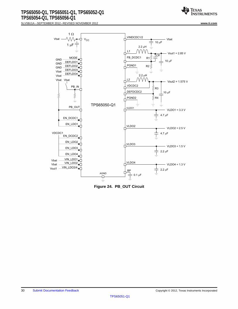
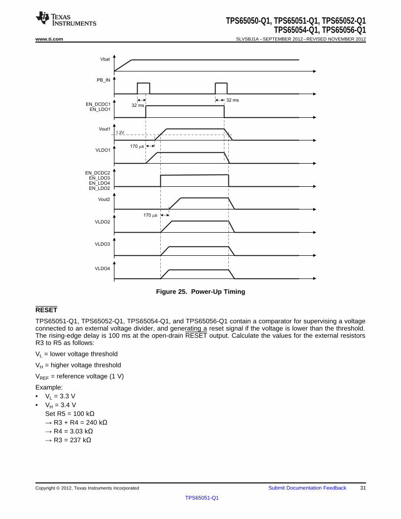
PB_IN and Sequencing
One can use the PB_OUT pin to enable one or several converters. After power up, the PB_OUT pin is low, andpulls down the enable pins connected to PB_OUT; EN_DCDC1, and EN_LDO1 in Figure 24. Pulling PB_IN toVCC for longer than 32 ms turns off the PB_OUT pin. Hence, a pullup resistor to VCC pulls the enable pins high,enabling the DCDC1 converter and LDO1. The enable signal for DCDC2 and LDO2 to LDO4 is the outputvoltage of DCDC1 (VOUT1). The battery (V(bat)) directly powers LDO1 with its output voltage of 3.3 V and LDO2for an output voltage of 2.5 V. To save power, the input voltage for the lower voltage rails at LDO3 and LDO4derives from the output of the step-down converters, keeping the voltage drop at the LDOs low to increaseefficiency. Because the output of DCDC1 powers LDO3 and LDO4, the total output current on VOUT1, LDO3, andLDO4 must not exceed the maximum rating of DCDC1.
Figure 25 shows the power up timing for this application.
www.ti.com SLVSBJ1A –SEPTEMBER 2012–REVISED NOVEMBER 2012
Figure 25. Power-Up Timing
RESET
TPS65051-Q1, TPS65052-Q1, TPS65054-Q1, and TPS65056-Q1 contain a comparator for supervising a voltageconnected to an external voltage divider, and generating a reset signal if the voltage is lower than the threshold.The rising-edge delay is 100 ms at the open-drain RESET output. Calculate the values for the external resistorsR3 to R5 as follows:
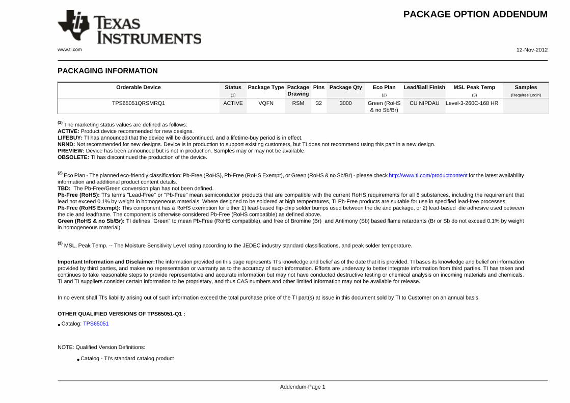
TPS65051QRSMRQ1 ACTIVE VQFN RSM 32 3000 Green (RoHS& no Sb/Br)
CU NIPDAU Level-3-260C-168 HR
(1) The marketing status values are defined as follows:ACTIVE: Product device recommended for new designs.LIFEBUY: TI has announced that the device will be discontinued, and a lifetime-buy period is in effect.NRND: Not recommended for new designs. Device is in production to support existing customers, but TI does not recommend using this part in a new design.PREVIEW: Device has been announced but is not in production. Samples may or may not be available.OBSOLETE: TI has discontinued the production of the device.
(2) Eco Plan - The planned eco-friendly classification: Pb-Free (RoHS), Pb-Free (RoHS Exempt), or Green (RoHS & no Sb/Br) - please check http://www.ti.com/productcontent for the latest availabilityinformation and additional product content details.TBD: The Pb-Free/Green conversion plan has not been defined.Pb-Free (RoHS): TI's terms "Lead-Free" or "Pb-Free" mean semiconductor products that are compatible with the current RoHS requirements for all 6 substances, including the requirement thatlead not exceed 0.1% by weight in homogeneous materials. Where designed to be soldered at high temperatures, TI Pb-Free products are suitable for use in specified lead-free processes.Pb-Free (RoHS Exempt): This component has a RoHS exemption for either 1) lead-based flip-chip solder bumps used between the die and package, or 2) lead-based die adhesive used betweenthe die and leadframe. The component is otherwise considered Pb-Free (RoHS compatible) as defined above.Green (RoHS & no Sb/Br): TI defines "Green" to mean Pb-Free (RoHS compatible), and free of Bromine (Br) and Antimony (Sb) based flame retardants (Br or Sb do not exceed 0.1% by weightin homogeneous material)
(3) MSL, Peak Temp. -- The Moisture Sensitivity Level rating according to the JEDEC industry standard classifications, and peak solder temperature.
Important Information and Disclaimer:The information provided on this page represents TI's knowledge and belief as of the date that it is provided. TI bases its knowledge and belief on informationprovided by third parties, and makes no representation or warranty as to the accuracy of such information. Efforts are underway to better integrate information from third parties. TI has taken andcontinues to take reasonable steps to provide representative and accurate information but may not have conducted destructive testing or chemical analysis on incoming materials and chemicals.TI and TI suppliers consider certain information to be proprietary, and thus CAS numbers and other limited information may not be available for release.
In no event shall TI's liability arising out of such information exceed the total purchase price of the TI part(s) at issue in this document sold by TI to Customer on an annual basis.
Texas Instruments Incorporated and its subsidiaries (TI) reserve the right to make corrections, enhancements, improvements and otherchanges to its semiconductor products and services per JESD46, latest issue, and to discontinue any product or service per JESD48, latestissue. Buyers should obtain the latest relevant information before placing orders and should verify that such information is current andcomplete. All semiconductor products (also referred to herein as “components”) are sold subject to TI’s terms and conditions of salesupplied at the time of order acknowledgment.
TI warrants performance of its components to the specifications applicable at the time of sale, in accordance with the warranty in TI’s termsand conditions of sale of semiconductor products. Testing and other quality control techniques are used to the extent TI deems necessaryto support this warranty. Except where mandated by applicable law, testing of all parameters of each component is not necessarilyperformed.
TI assumes no liability for applications assistance or the design of Buyers’ products. Buyers are responsible for their products andapplications using TI components. To minimize the risks associated with Buyers’ products and applications, Buyers should provideadequate design and operating safeguards.
TI does not warrant or represent that any license, either express or implied, is granted under any patent right, copyright, mask work right, orother intellectual property right relating to any combination, machine, or process in which TI components or services are used. Informationpublished by TI regarding third-party products or services does not constitute a license to use such products or services or a warranty orendorsement thereof. Use of such information may require a license from a third party under the patents or other intellectual property of thethird party, or a license from TI under the patents or other intellectual property of TI.
Reproduction of significant portions of TI information in TI data books or data sheets is permissible only if reproduction is without alterationand is accompanied by all associated warranties, conditions, limitations, and notices. TI is not responsible or liable for such altereddocumentation. Information of third parties may be subject to additional restrictions.
Resale of TI components or services with statements different from or beyond the parameters stated by TI for that component or servicevoids all express and any implied warranties for the associated TI component or service and is an unfair and deceptive business practice.TI is not responsible or liable for any such statements.
Buyer acknowledges and agrees that it is solely responsible for compliance with all legal, regulatory and safety-related requirementsconcerning its products, and any use of TI components in its applications, notwithstanding any applications-related information or supportthat may be provided by TI. Buyer represents and agrees that it has all the necessary expertise to create and implement safeguards whichanticipate dangerous consequences of failures, monitor failures and their consequences, lessen the likelihood of failures that might causeharm and take appropriate remedial actions. Buyer will fully indemnify TI and its representatives against any damages arising out of the useof any TI components in safety-critical applications.
In some cases, TI components may be promoted specifically to facilitate safety-related applications. With such components, TI’s goal is tohelp enable customers to design and create their own end-product solutions that meet applicable functional safety standards andrequirements. Nonetheless, such components are subject to these terms.
No TI components are authorized for use in FDA Class III (or similar life-critical medical equipment) unless authorized officers of the partieshave executed a special agreement specifically governing such use.
Only those TI components which TI has specifically designated as military grade or “enhanced plastic” are designed and intended for use inmilitary/aerospace applications or environments. Buyer acknowledges and agrees that any military or aerospace use of TI componentswhich have not been so designated is solely at the Buyer's risk, and that Buyer is solely responsible for compliance with all legal andregulatory requirements in connection with such use.
TI has specifically designated certain components which meet ISO/TS16949 requirements, mainly for automotive use. Components whichhave not been so designated are neither designed nor intended for automotive use; and TI will not be responsible for any failure of suchcomponents to meet such requirements.
Products Applications
Audio www.ti.com/audio Automotive and Transportation www.ti.com/automotive
Amplifiers amplifier.ti.com Communications and Telecom www.ti.com/communications
Data Converters dataconverter.ti.com Computers and Peripherals www.ti.com/computers