DATASHEET 9FGV0631C JUNE 6, 2019 1 6-Output Very Low-Power PCIe Gen 1-2-3-4 Clock Generator 9FGV0631C Description The 9FGV0631C is a member of IDT's SOC-Friendly 1.8V very low-power PCIe clock family. The device has 6 output enables for clock management, 2 different spread spectrum levels in addition to spread off, and 2 selectable SMBus addresses. Typical Applications PCIe Gen1–4 clock generation for Riser Cards, Storage, Networking, JBOD, Communications, Access Points Output Features • 6 100MHz Low-Power (LP) HCSL DIF pairs • 1 1.8V LVCMOS REF output w/Wake-On-LAN (WOL) support Key Specifications • DIF cycle-to-cycle jitter <50ps • DIF output-to-output skew <50ps • DIF phase jitter is PCIe Gen1-2-3-4 compliant • REF phase jitter is < 1.5ps RMS Features • LP-HCSL outputs; save 12 resistors compared to standard PCIe devices • 54mW typical power consumption; reduced thermal concerns • Outputs can optionally be supplied from any voltage between 1.05V and 1.8V; maximum power savings • OE# pins; support DIF power management • Programmable slew rate for each output; allows tuning for various line lengths • Programmable output amplitude; allows tuning for various application environments • DIF outputs blocked until PLL is locked; clean system start-up • Selectable 0%, -0.25% or -0.5% spread on DIF outputs; reduces EMI • External 25MHz crystal; supports tight ppm with 0 ppm synthesis error • Configuration can be accomplished with strapping pins; SMBus interface not required for device control • 3.3V tolerant SMBus interface works with legacy controllers • Selectable SMBus addresses; multiple devices can easily share an SMBus segment • Space saving 5 x 5 mm 40-VFQFPN; minimal board space Block Diagram XIN/CLKIN_25 X2 CONTROL LOGIC vSS_EN_tri ^CKPWRGD_PD# SDATA_3.3 SS Capable PLL OSC REF1.8 vOE(5:0)# SCLK_3.3 vSADR DIF5 DIF4 DIF3 DIF2 DIF1 DIF0
Transcript
DATASHEET
9FGV0631C JUNE 6, 2019 1
6-Output Very Low-Power PCIe Gen 1-2-3-4Clock Generator
9FGV0631C
DescriptionThe 9FGV0631C is a member of IDT's SOC-Friendly 1.8V very low-power PCIe clock family. The device has 6 output enables for clock management, 2 different spread spectrum levels in addition to spread off, and 2 selectable SMBus addresses.
1. REF is Hi-Z until the 1st assertion of CKPWRGD_PD# high. After this, whenCKPWRG_PD# is low, REF is Low.
Pin NumberVDD VDDIO GND
4 41 XTAL OSC5 41 REF Power
11 8Digital (dirty)
Power12,17,27,32,39 41 DIF outputs
26 41 PLL Analog
Description
JUNE 6, 2019 3 6-OUTPUT VERY LOW-POWER PCIE GEN 1-2-3-4 CLOCK GENERATOR
9FGV0631C DATASHEET
Pin DescriptionsPIN # PIN NAME PIN TYPE DESCRIPTION
1 vSS_EN_triLATCHED
INLatched select input to select spread spectrum amount at initial power up :1 = -0.5% spread, M = -0.25%, 0 = Spread Off
2 X1_25 IN Crystal input, Nominally 25.00MHz. 3 X2 OUT Crystal output.4 VDDXTAL1.8 PWR Power supply for XTAL, nominal 1.8V5 VDDREF1.8 PWR VDD for REF output. nominal 1.8V.
6 vSADR/REF1.8 LATCHED
I/OLatch to select SMBus Address/1.8V LVCMOS copy of X1/REFIN pin
7 NC N/A No Connection.8 GNDDIG GND Ground pin for digital circuitry9 SCLK_3.3 IN Clock pin of SMBus circuitry, 3.3V tolerant. 10 SDATA_3.3 I/O Data pin for SMBus circuitry, 3.3V tolerant. 11 VDDDIG1.8 PWR 1.8V digital power (dirty power)12 VDDIO PWR Power supply for differential outputs
13 vOE0# INActive low input for enabling DIF pair 0. This pin has an internal pull-down.1 =disable outputs, 0 = enable outputs
14 DIF0 OUT Differential true clock output15 DIF0# OUT Differential Complementary clock output16 VDD1.8 PWR Power supply, nominal 1.8V17 VDDIO PWR Power supply for differential outputs18 DIF1 OUT Differential true clock output19 DIF1# OUT Differential Complementary clock output20 NC N/A No Connection.
21 vOE1# INActive low input for enabling DIF pair 1. This pin has an internal pull-down.1 =disable outputs, 0 = enable outputs
22 DIF2 OUT Differential true clock output23 DIF2# OUT Differential Complementary clock output
24 vOE2# INActive low input for enabling DIF pair 2. This pin has an internal pull-down. 1 =disable outputs, 0 = enable outputs
25 NC N/A No Connection.26 VDDA1.8 PWR 1.8V power for the PLL core.27 VDDIO PWR Power supply for differential outputs28 DIF3 OUT Differential true clock output29 DIF3# OUT Differential Complementary clock output
30 vOE3# INActive low input for enabling DIF pair 3. This pin has an internal pull-down. 1 =disable outputs, 0 = enable outputs
31 VDD1.8 PWR Power supply, nominal 1.8V32 VDDIO PWR Power supply for differential outputs33 DIF4 OUT Differential true clock output34 DIF4# OUT Differential Complementary clock output
35 vOE4# INActive low input for enabling DIF pair 4. This pin has an internal pull-down. 1 =disable outputs, 0 = enable outputs
36 DIF5 OUT Differential true clock output37 DIF5# OUT Differential Complementary clock output
38 vOE5# INActive low input for enabling DIF pair 5. This pin has an internal pull-down.1 =disable outputs, 0 = enable outputs
39 VDDIO PWR Power supply for differential outputs
40 ^CKPWRGD_PD# INInput notifies device to sample latched inputs and start up on first high assertion. Low enters Power Down Mode, subsequent high assertions exit Power Down Mode. This pin has internal pull-up resistor.
41 ePAD GND Connect paddle to ground.
6-OUTPUT VERY LOW-POWER PCIE GEN 1-2-3-4 CLOCK GENERATOR 4 JUNE 6, 2019
9FGV0631C DATASHEET
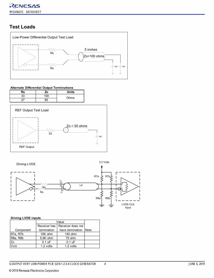
Test Loads
Alternate Differential Output TerminationsRs Zo Units33 10027 85
JUNE 6, 2019 5 6-OUTPUT VERY LOW-POWER PCIE GEN 1-2-3-4 CLOCK GENERATOR
9FGV0631C DATASHEET
Absolute Maximum Ratings
Stresses above the ratings listed below can cause permanent damage to the 9FGV0631C. These ratings, which are standard values for IDT commercially rated parts, are stress ratings only. Functional operation of the device at these or any other conditions above those indicated in the operational sections of the specifications is not implied. Exposure to absolute maximum rating conditions for extended periods can affect product reliability. Electrical parameters are guaranteed only over the recommended operating temperature range.
Electrical Characteristics–Current Consumption
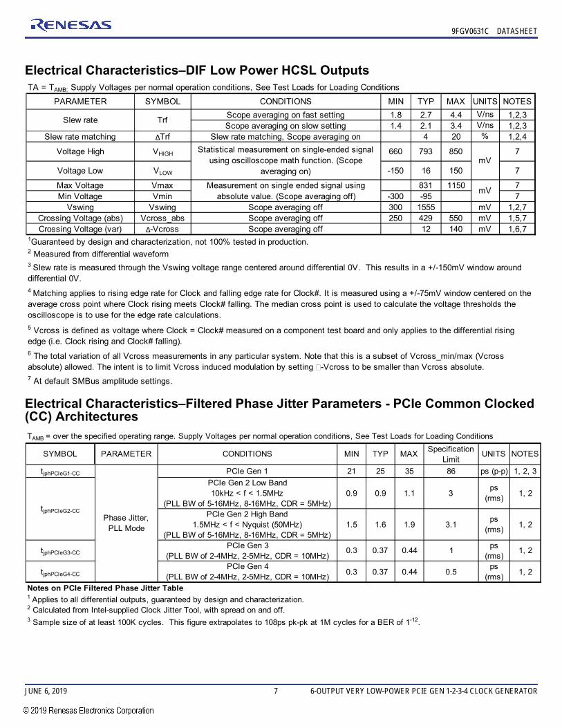
Electrical Characteristics–DIF Output Duty Cycle, Jitter, and Skew Characteristics
PARAMETER SYMBOL CONDITIONSMIN TYP MAX
UNITS NOTES
Supply Voltage VDDxx Applies to all VDD pins -0.5 2.5 V 1,2Input Voltage VIN -0.5 VDD+0.5V V 1, 3
Input High Voltage, SMBus VIHSMB SMBus clock and data pins 3.6V V 1Storage Temperature Ts -65 150 °C 1Junction Temperature Tj 125 °C 1Input ESD protection ESD prot Human Body Model 2000 V 1
1Guaranteed by design and characterization, not 100% tested in production.2 Operation under these conditions is neither implied nor guaranteed.3 Not to exceed 2.5V.
TA = TAMB; Supply Voltages per normal operation conditions, See Test Loads for Loading Conditions
PARAMETER SYMBOL CONDITIONS MIN TYP MAX UNITS NOTES
IDDAOP VDDA, All outputs active @100MHz 6.1 9 mA
IDDOPAll VDD, except VDDA and VDDIO, All outputs
active @100MHz10.5 15 mA
IDDIOOP VDDIO, All outputs active @100MHz 22 30 mA
IDDPD All VDD, except VDDA and VDDIO, all outputs off 0.6 1 mA
IDDIOPD VDDIO, all outputs off 0.0003 0.1 mA1 Guaranteed by design and characterization, not 100% tested in production.2 This is the current required to have the REF output running in Wake-on-LAN mode (Byte 3, bit 5 = 1)
Operating Supply Current
Wake-on-LAN Current(CKPWRGD_PD# = '0'
Byte 3, bit 5 = '1')
Powerdown Current(CKPWRGD_PD# = '0'
Byte 3, bit 5 = '0')
TA = TAMB; Supply Voltages per normal operation conditions, See Test Loads for Loading Conditions
PARAMETER SYMBOL CONDITIONS MIN TYP MAX UNITS NOTES
Skew, Output to Output tsk3 Averaging on, VT = 50% 37 50 ps 1,2
Jitter, Cycle to cycle tjcyc-cyc 12 50 ps 1,21Guaranteed by design and characterization, not 100% tested in production.2 Measured from differential waveform
6-OUTPUT VERY LOW-POWER PCIE GEN 1-2-3-4 CLOCK GENERATOR 6 JUNE 6, 2019
9FGV0631C DATASHEET
Electrical Characteristics–Input/Supply/Common Output Parameters–Normal Operating ConditionsTA = TAMB; Supply Voltages per normal operation conditions, See Test Loads for Loading Conditions
PARAMETER SYMBOL CONDITIONS MIN TYP MAX UNITS NOTES
Supply Voltage VDDxxSupply voltage for core, analog and single-ended
LVCMOS outputs1.7 1.8 1.9 V
Output Supply Voltage VDDIO Supply voltage for differential Low Power Outputs 0.9975 1.05-1.8 1.9 V
Commercial range 0 25 70 °CIndustrial range -40 25 85 °C
Input High Voltage VIH Single-ended inputs, except SMBus 0.75 VDD VDD + 0.3 V
Input Mid Voltage VIM Single-ended tri-level inputs ('_tri' suffix) 0.4 VDD 0.5 VDD 0.6 VDD V
Input Low Voltage VIL Single-ended inputs, except SMBus -0.3 0.25 VDD V
Output High Voltage VIH Single-ended outputs, except SMBus. IOH = -2mA VDD-0.45 V
Output Low Voltage VIL Single-ended outputs, except SMBus. IOL = -2mA 0.45 V
Max Voltage Vmax 831 1150 7Min Voltage Vmin -300 -95 7
Vswing Vswing Scope averaging off 300 1555 mV 1,2,7Crossing Voltage (abs) Vcross_abs Scope averaging off 250 429 550 mV 1,5,7Crossing Voltage (var) Δ-Vcross Scope averaging off 12 140 mV 1,6,7
2 Measured from differential waveform
7 At default SMBus amplitude settings.
1Guaranteed by design and characterization, not 100% tested in production.
3 Slew rate is measured through the Vswing voltage range centered around differential 0V. This results in a +/-150mV window around differential 0V. 4 Matching applies to rising edge rate for Clock and falling edge rate for Clock#. It is measured using a +/-75mV window centered on the average cross point where Clock rising meets Clock# falling. The median cross point is used to calculate the voltage thresholds the oscilloscope is to use for the edge rate calculations.
5 Vcross is defined as voltage where Clock = Clock# measured on a component test board and only applies to the differential rising edge (i.e. Clock rising and Clock# falling).6 The total variation of all Vcross measurements in any particular system. Note that this is a subset of Vcross_min/max (Vcross absolute) allowed. The intent is to limit Vcross induced modulation by setting -Vcross to be smaller than Vcross absolute.
Slew rate Trf
Statistical measurement on single-ended signal using oscilloscope math function. (Scope
averaging on)mV
Measurement on single ended signal using absolute value. (Scope averaging off)
mV
TAMB = over the specified operating range. Supply Voltages per normal operation conditions, See Test Loads for Loading Conditions
SYMBOL PARAMETER CONDITIONS MIN TYP MAXSpecification
Notes on PCIe Filtered Phase Jitter Table1 Applies to all differential outputs, guaranteed by design and characterization.
Phase Jitter, PLL Mode
tjphPCIeG2-CC
2 Calculated from Intel-supplied Clock Jitter Tool, with spread on and off.3 Sample size of at least 100K cycles. This figure extrapolates to 108ps pk-pk at 1M cycles for a BER of 1-12.
6-OUTPUT VERY LOW-POWER PCIE GEN 1-2-3-4 CLOCK GENERATOR 8 JUNE 6, 2019
9FGV0631C DATASHEET
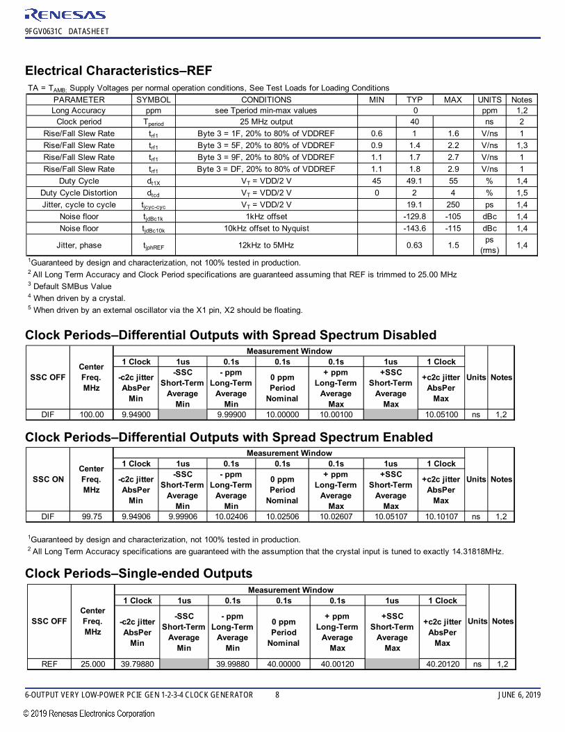
Electrical Characteristics–REF
Clock Periods–Differential Outputs with Spread Spectrum Disabled
Clock Periods–Differential Outputs with Spread Spectrum Enabled
Clock Periods–Single-ended Outputs
TA = TAMB; Supply Voltages per normal operation conditions, See Test Loads for Loading Conditions
PARAMETER SYMBOL CONDITIONS MIN TYP MAX UNITS NotesLong Accuracy ppm see Tperiod min-max values ppm 1,2
Clock period Tperiod 25 MHz output 40 ns 2
Rise/Fall Slew Rate trf1 Byte 3 = 1F, 20% to 80% of VDDREF 0.6 1 1.6 V/ns 1
Rise/Fall Slew Rate trf1 Byte 3 = 5F, 20% to 80% of VDDREF 0.9 1.4 2.2 V/ns 1,3
Rise/Fall Slew Rate trf1 Byte 3 = 9F, 20% to 80% of VDDREF 1.1 1.7 2.7 V/ns 1
Rise/Fall Slew Rate trf1 Byte 3 = DF, 20% to 80% of VDDREF 1.1 1.8 2.9 V/ns 1
1Guaranteed by design and characterization, not 100% tested in production.2 All Long Term Accuracy specifications are guaranteed with the assumption that the crystal input is tuned to exactly 14.31818MHz.
1. A low on these bits will override the OE# pin and force the differential output Low/Low
SMBus Table: SS Readback and Control RegisterByte 1 Name Control Function Type 0 1 DefaultBit 7 SSENRB1 SS Enable Readback Bit1 R LatchBit 6 SSENRB1 SS Enable Readback Bit0 R Latch
Bit 5 SSEN_SWCNTRL Enable SW control of SS RWValues in B1[7:6]
control SS amountValues in B1[4:3] control SS amount.
SMBus Table: Revision and Vendor ID RegisterByte 5 Name Control Function Type 0 1 DefaultBit 7 RID3 R 0Bit 6 RID2 R 0Bit 5 RID1 R 0Bit 4 RID0 R 1Bit 3 VID3 R 0Bit 2 VID2 R 0Bit 1 VID1 R 0Bit 0 VID0 R 1
SMBus Table: Device Type/Device IDByte 6 Name Control Function Type 0 1 DefaultBit 7 Device Type1 R 0Bit 6 Device Type0 R 0Bit 5 Device ID5 R 0Bit 4 Device ID4 R 0Bit 3 Device ID3 R 0Bit 2 Device ID2 R 1Bit 1 Device ID1 R 1Bit 0 Device ID0 R 0
SMBus Table: Byte Count RegisterByte 7 Name Control Function Type 0 1 DefaultBit 7 0Bit 6 0Bit 5 0Bit 4 BC4 RW 0Bit 3 BC3 RW 1Bit 2 BC2 RW 0Bit 1 BC1 RW 0Bit 0 BC0 RW 0
C rev = 0001Revision ID
Writing to this register will configure how many bytes will be read back, default is
= 8 bytes.
VENDOR ID
Byte Count Programming
Reserved
00 = FGx, 01 = DBx ZDB/FOB, 10 = DMx, 11= DBx FOB
Reserved
Device Type
000110 binary or 06 hexDevice ID
Reserved
0001 = IDT
PARAMETER VALUE UNITS NOTES
Frequency 25 MHz 1Resonance Mode Fundamental - 1
Frequency Tolerance @ 25°C ±20 PPM Max 1Frequency Stability, ref @ 25°C Over
Operating Temperature Range±20 PPM Max 1
Temperature Range (commercial) 0~70 °C 1Temperature Range (industrial) -40~85 °C 2
Equivalent Series Resistance (ESR) 50 Ω Max 1Shunt Capacitance (CO) 7 pF Max 1
Load Capacitance (CL) 8 pF Max 1Drive Level 0.3 mW Max 1
Aging per year ±5 PPM Max 1
Notes:1. FOX 603-25-150.2. For I-temp, FOX 603-25-261.
6-OUTPUT VERY LOW-POWER PCIE GEN 1-2-3-4 CLOCK GENERATOR 12 JUNE 6, 2019
9FGV0631C DATASHEET
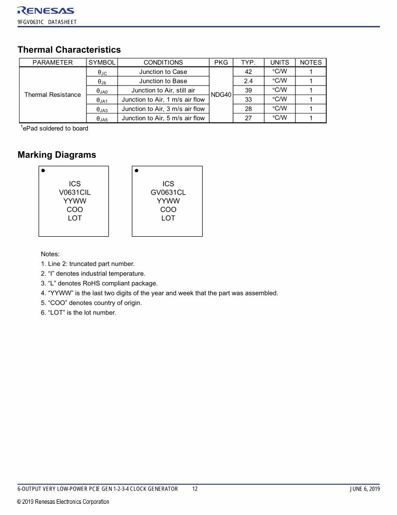
Thermal Characteristics
Marking Diagrams
Notes:
1. Line 2: truncated part number.
2. “I” denotes industrial temperature.
3. “L” denotes RoHS compliant package.
4. “YYWW” is the last two digits of the year and week that the part was assembled.
5. “COO” denotes country of origin.
6. “LOT” is the lot number.
PARAMETER SYMBOL CONDITIONS PKG TYP. UNITS NOTES
θJC Junction to Case 42 °C/W 1
θJb Junction to Base 2.4 °C/W 1
θJA0 Junction to Air, still air 39 °C/W 1
θJA1 Junction to Air, 1 m/s air flow 33 °C/W 1
θJA3 Junction to Air, 3 m/s air flow 28 °C/W 1
θJA5 Junction to Air, 5 m/s air flow 27 °C/W 1
Thermal Resistance NDG40
1ePad soldered to board
ICSV0631CIL
YYWWCOOLOT
ICSGV0631CL
YYWWCOOLOT
JUNE 6, 2019 13 6-OUTPUT VERY LOW-POWER PCIE GEN 1-2-3-4 CLOCK GENERATOR
9FGV0631C DATASHEET
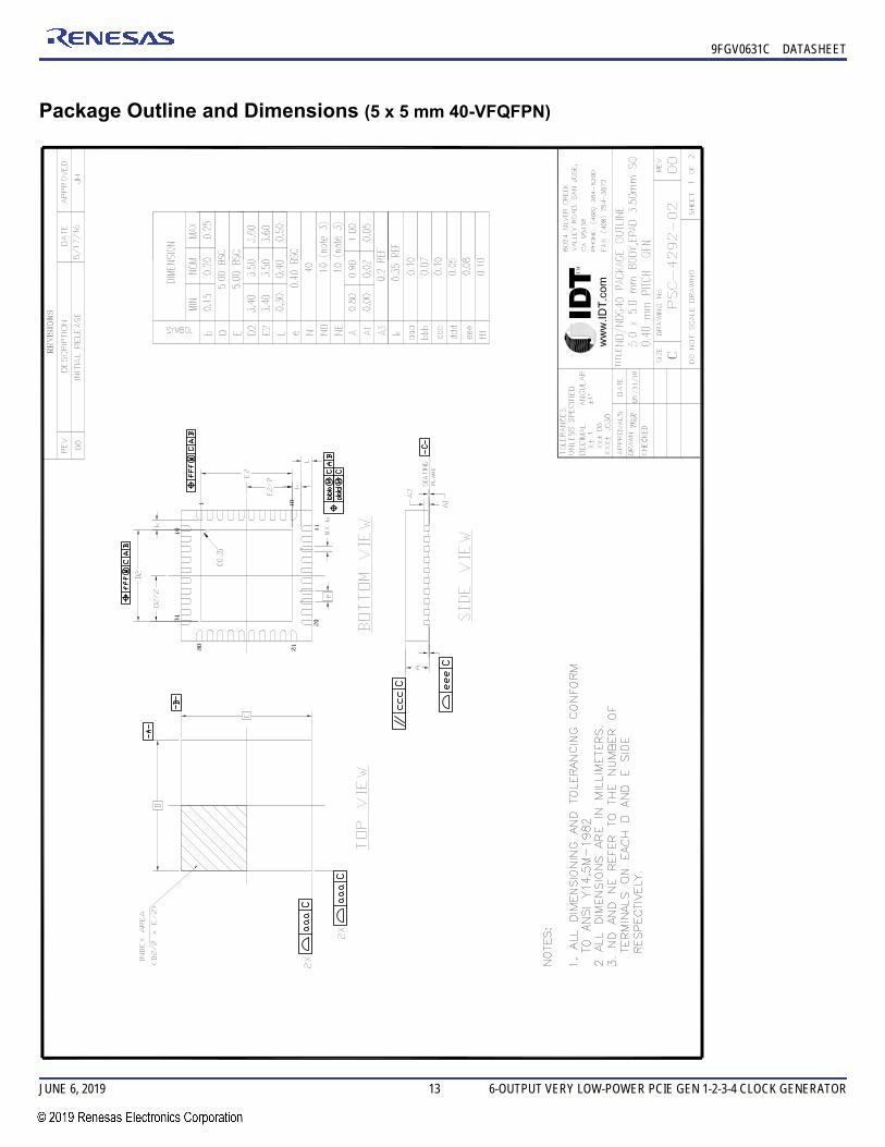
Package Outline and Dimensions (5 x 5 mm 40-VFQFPN)
6-OUTPUT VERY LOW-POWER PCIE GEN 1-2-3-4 CLOCK GENERATOR 14 JUNE 6, 2019
9FGV0631C DATASHEET
Package Outline and Dimensions (5 x 5 mm 40-VFQFPN), cont.
JUNE 6, 2019 15 6-OUTPUT VERY LOW-POWER PCIE GEN 1-2-3-4 CLOCK GENERATOR
9FGV0631C DATASHEET
Ordering Information
“LF” suffix to the part number are the Pb-Free configuration and are RoHS compliant.
“C” is the device revision designator (will not correlate with the datasheet revision).
Revision History
Part / Order Number Shipping Packaging Package Temperature9FGV0631CKLF Trays 40-pin VFQFPN 0 to +70° C
9FGV0631CKLFT Tape and Reel 40-pin VFQFPN 0 to +70° C9FGV0631CKILF Trays 40-pin VFQFPN -40 to +85° C9FGV0631CKILFT Tape and Reel 40-pin VFQFPN -40 to +85° C
Issue Date Description
September 29, 2014
1. Updated front page text and block diagram.2. Updated pin out to remove references to VDD Suspend pins. Using the part with collapsiblepower supplies did not save power and complicated board design. NO pins were changed.3. Updated SMBus Descriptions4. Simplified footnote 2 on PPM table.5. Updated all electrical tables6. Move to final
October 18, 2016 Removed IDT crystal part number
June 23, 2017Updated front page Gendes to reflect the PCIe Gen4 updates.Updated Electrical Characteristics - Filtered Phase Jitter Parameters - PCIe Common Clocked (CC) Architectures and added PCIe Gen4 Data
June 6, 2019 Changed Input Current minimum and maximum values from -200/200uA to -20/20uA.
DISCLAIMER Integrated Device Technology, Inc. (IDT) and its affiliated companies (herein referred to as “IDT”) reserve the right to modify the products and/or specifications described herein at any time, withoutnotice, at IDT’s sole discretion. Performance specifications and operating parameters of the described products are determined in an independent state and are not guaranteed to perform the same way when installedin customer products. The information contained herein is provided without representation or warranty of any kind, whether express or implied, including, but not limited to, the suitability of IDT's products for anyparticular purpose, an implied warranty of merchantability, or non-infringement of the intellectual property rights of others. This document is presented only as a guide and does not convey any license under intel-lectual property rights of IDT or any third parties.
IDT's products are not intended for use in applications involving extreme environmental conditions or in life support systems or similar devices where the failure or malfunction of an IDT product can be reasonablyexpected to significantly affect the health or safety of users. Anyone using an IDT product in such a manner does so at their own risk, absent an express, written agreement by IDT.
Integrated Device Technology, IDT and the IDT logo are trademarks or registered trademarks of IDT and its subsidiaries in the United States and other countries. Other trademarks used herein are the property ofIDT or their respective third party owners. For datasheet type definitions and a glossary of common terms, visit www.idt.com/go/glossary. Integrated Device Technology, Inc. All rights reserved.
Corporate Headquarters6024 Silver Creek Valley Road San Jose, CA 95138 USAwww.IDT.com
Sales1-800-345-7015 or 408-284-8200Fax: 408-284-2775www.IDT.com/go/sales
Corporate HeadquartersTOYOSU FORESIA, 3-2-24 Toyosu,Koto-ku, Tokyo 135-0061, Japanwww.renesas.com
Contact InformationFor further information on a product, technology, the most up-to-date version of a document, or your nearest sales office, please visit:www.renesas.com/contact/
TrademarksRenesas and the Renesas logo are trademarks of Renesas Electronics Corporation. All trademarks and registered trademarks are the property of their respective owners.
IMPORTANT NOTICE AND DISCLAIMER
RENESAS ELECTRONICS CORPORATION AND ITS SUBSIDIARIES (“RENESAS”) PROVIDES TECHNICAL SPECIFICATIONS AND RELIABILITY DATA (INCLUDING DATASHEETS), DESIGN RESOURCES (INCLUDING REFERENCE DESIGNS), APPLICATION OR OTHER DESIGN ADVICE, WEB TOOLS, SAFETY INFORMATION, AND OTHER RESOURCES “AS IS” AND WITH ALL FAULTS, AND DISCLAIMS ALL WARRANTIES, EXPRESS OR IMPLIED, INCLUDING, WITHOUT LIMITATION, ANY IMPLIED WARRANTIES OF MERCHANTABILITY, FITNESS FOR A PARTICULAR PURPOSE, OR NON-INFRINGEMENT OF THIRD PARTY INTELLECTUAL PROPERTY RIGHTS.
These resources are intended for developers skilled in the art designing with Renesas products. You are solely responsible for (1) selecting the appropriate products for your application, (2) designing, validating, and testing your application, and (3) ensuring your application meets applicable standards, and any other safety, security, or other requirements. These resources are subject to change without notice. Renesas grants you permission to use these resources only for development of an application that uses Renesas products. Other reproduction or use of these resources is strictly prohibited. No license is granted to any other Renesas intellectual property or to any third party intellectual property. Renesas disclaims responsibility for, and you will fully indemnify Renesas and its representatives against, any claims, damages, costs, losses, or liabilities arising out of your use of these resources. Renesas' products are provided only subject to Renesas' Terms and Conditions of Sale or other applicable terms agreed to in writing. No use of any Renesas resources expands or otherwise alters any applicable warranties or warranty disclaimers for these products.