This material is posted here with permission of the IEEE. Such permission of the IEEE does not in any way imply IEEE endorsement of any of Cree’s products or services. Internal or personal use of this material is permitted. However, permission to reprint/republish this material for advertis-ing or promotional purposes or for creating new collective works for resale or redistribution must be obtained from the IEEE by writing to [email protected] By choosing to view this document, you agree to all provisions of the copyright laws protecting it.
6-Port GaN HEMT Models Help Designers Optimize PA Efficiency
Waveform Engineering Maximizes Wireless PA Performance
Simulation of power amplifiers (PAs) for modern wireless base station and small cell systems isan essential part of the design process. At a cell site, the PA consumes the bulk of the DC power,generates the most heat, and thus represents the greatest operational cost. Maximum PA effi-ciency is a necessity to manage these costs, which is a sizeable challenge in a PA that also mustbe highly linear to support the complex multi-level modulation types and wide bandwidths usedfor current and developing wireless transmission standards. Accurate simulation allows the PAdesigner to meet these challenges by exploring the available design options, then optimizing thecircuit that is selected for the application.
High performance power devices such as GaN HEMTs are combined with sophisticated circuitarchitectures to achieve the necessary efficiency and linearity. The PA may use any of severaldifferent design methods — Doherty, envelope tracking, outphasing, or any of several extensionsand hybrid structures — but in each case it must be optimized for the highest efficiency whilemaintaining all other desired performance characteristics.
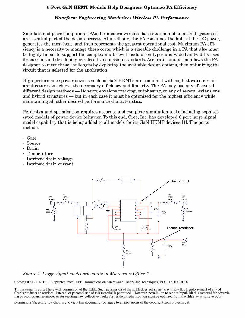
PA design and optimization requires accurate and complete simulation tools, including sophisti-cated models of power device behavior. To this end, Cree, Inc. has developed 6 port large signalmodel capability that is being added to all models for its GaN HEMT devices [1]. The portsinclude:
This material is posted here with permission of the IEEE. Such permission of the IEEE does not in any way imply IEEE endorsement of any of Cree’s products or services. Internal or personal use of this material is permitted. However, permission to reprint/republish this material for advertis-ing or promotional purposes or for creating new collective works for resale or redistribution must be obtained from the IEEE by writing to [email protected] By choosing to view this document, you agree to all provisions of the copyright laws protecting it.
The models are compatible with both Agilent’s ADS and AWR’s Microwave Office design suites.The complete model in Microwave Office™ is shown in Figure 1. The core large-signal model isbased on established equivalent circuit methods, with data extracted in various test fixtures andtest circuits, including load pull at the fundamental and harmonics.
The intrinsic drain current and intrinsic drain voltage ports are newly-developed additions tothe device model. Intrinsic means that these virtual ports are located right at the active device,without the effects of package parasitics. To the designer, these intrinsic ports act as voltage andcurrent probes right at the die. This ability to observe the voltage and current waveforms isessential to verify the PA’s class of operation and to optimize device matching at fundamentaland harmonic frequencies.
In addition, observing drain voltage is important for investigation of drain voltage switching,peak voltage excursions or drain modulation, as is used in multi-level Doherty and envelope-tracking PAs. Also, circuit robustness can be evaluated by observing peak voltages during highVSWR conditions.
Unlike traditional classes A, B and C that are defined by device bias conditions and sine wavesignals, high efficiency classes of operation (classes E, F, and others) utilize the active device asa switch. Performance is defined by the relationship between current and voltage, including theshape of the waveforms, which is a function of the energy at harmonic frequencies. The PAdesigner must develop input and output bias and matching networks that fulfill the require-ments for the desired class of operation. Optimized design, where practical implementationapproaches ideal behavior, can only be accomplished when the PA engineer can observe theactual drain voltage and current waveforms in addition to the traditional parameters of inputpower, output power, DC power and bias.
Readers are certainly aware that digital predistortion (DPD) is a critical part of achieving thenecessary linearity for accurate signal modulation and minimum off-channel energy that caninterfere with other users. They should note that DPD is intended to be the final step in the lin-earization process. It is most effective when the uncorrected path through the amplifier chainhas the highest performance obtainable.
Class F and Inverse Class F Operation
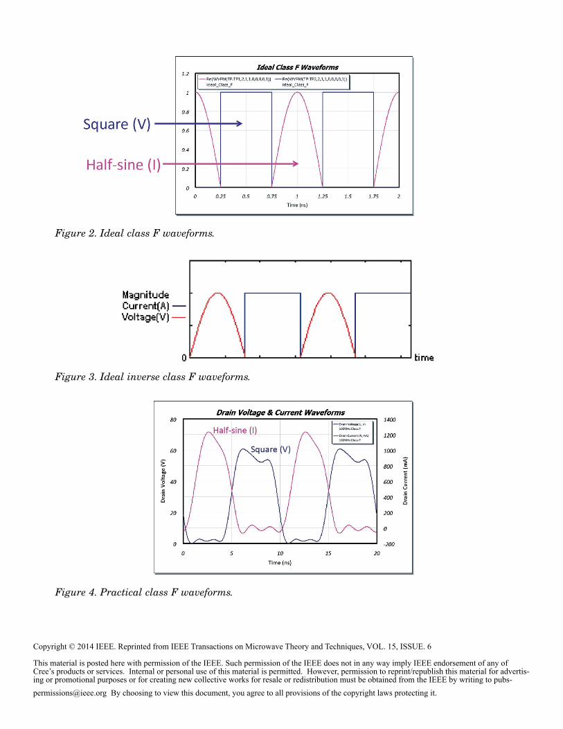
Presently, class F and inverse class F are favored for high efficiency designs. For ideal class Foperation, the drain voltage waveform is a square wave and the current waveform is a half-sine(Figure 2) [2]. Ideal inverse class F operation, as the name implies, has a square wave currentwaveform and a half-sine voltage waveform (Figure 3) [3]. Ideal square waves contain an infinitenumber of harmonics which is not possible in a practical PA. However, a small number of oddharmonics (e.g., 3rd and 5th harmonic) will result in a sufficient approximation of a square waveto obtain high power added efficiency (PAE). Figures 4 and 5 show practical waveforms for classF and inverse class F PAs.
This material is posted here with permission of the IEEE. Such permission of the IEEE does not in any way imply IEEE endorsement of any of Cree’s products or services. Internal or personal use of this material is permitted. However, permission to reprint/republish this material for advertis-ing or promotional purposes or for creating new collective works for resale or redistribution must be obtained from the IEEE by writing to [email protected] By choosing to view this document, you agree to all provisions of the copyright laws protecting it.
This material is posted here with permission of the IEEE. Such permission of the IEEE does not in any way imply IEEE endorsement of any of Cree’s products or services. Internal or personal use of this material is permitted. However, permission to reprint/republish this material for advertis-ing or promotional purposes or for creating new collective works for resale or redistribution must be obtained from the IEEE by writing to [email protected] By choosing to view this document, you agree to all provisions of the copyright laws protecting it.
Figure 5. Practical inverse class F waveforms.
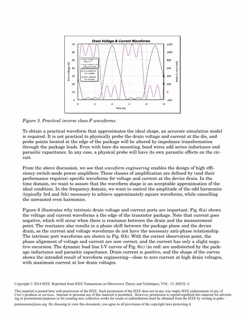
To obtain a practical waveform that approximates the ideal shape, an accurate simulation modelis required. It is not practical to physically probe the drain voltage and current at the die, andprobe points located at the edge of the package will be altered by impedance transformationthrough the package leads. Even with bare die mounting, bond wires add series inductance andparasitic capacitance. In any case, a physical probe will have its own parasitic effects on the cir-cuit.
From the above discussion, we see that waveform engineering enables the design of high effi-ciency switch-mode power amplifiers. These classes of amplification are defined by (and theirperformance requires) specific waveforms for voltage and current at the device drain. In thetime domain, we want to assure that the waveform shape is an acceptable approximation of theideal condition. In the frequency domain, we want to control the amplitude of the odd harmonics(typically 3rd and 5th) necessary to achieve approximately square waveforms, while cancellingthe unwanted even harmonics.
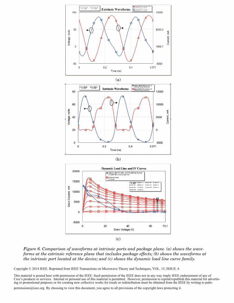
Figure 6 illustrates why intrinsic drain voltage and current ports are important. Fig. 6(a) showsthe voltage and current waveforms a the edge of the transistor package. Note that current goesnegative, which will occur when there is reactance between the drain and the measurementpoint. The reactance also results in a phase shift between the package plane and the devicedrain, as the current and voltage waveforms do not have the necessary anti-phase relationship.The intrinsic port waveforms are shown in Fig. 6(b). With the correct observation point, thephase alignment of voltage and current are now correct, and the current has only a slight nega-tive excursion. The dynamic load line I-V curves of Fig. 6(c) (in red) are undistorted by the pack-age inductance and parasitic capacitance. Drain current is positive, and the shape of the curvesshows the intended result of waveform engineering—close to zero current at high drain voltages,with maximum current at low drain voltages.
This material is posted here with permission of the IEEE. Such permission of the IEEE does not in any way imply IEEE endorsement of any of Cree’s products or services. Internal or personal use of this material is permitted. However, permission to reprint/republish this material for advertis-ing or promotional purposes or for creating new collective works for resale or redistribution must be obtained from the IEEE by writing to [email protected] By choosing to view this document, you agree to all provisions of the copyright laws protecting it.
(a)
(b)
(c)
Figure 6. Comparison of waveforms at intrinsic ports and package plane. (a) shows the wave-forms at the extrinsic reference plane that includes package effects; (b) shows the waveforms atthe intrinsic port located at the device; and (c) shows the dynamic load line curve family.
This material is posted here with permission of the IEEE. Such permission of the IEEE does not in any way imply IEEE endorsement of any of Cree’s products or services. Internal or personal use of this material is permitted. However, permission to reprint/republish this material for advertis-ing or promotional purposes or for creating new collective works for resale or redistribution must be obtained from the IEEE by writing to [email protected] By choosing to view this document, you agree to all provisions of the copyright laws protecting it.
Finally, the desired waveform must be achieved using the impedance transformation networksat input and output. Synthesis, optimization and realization of a matching network that oper-ates over the desired bandwidth is the traditional work of an RF PA engineer, and has becomeincreasingly difficult with the additional requirements of proper harmonic response for the PAclass of operation and the wider bandwidth required for high data rate wireless communicationssystems.
2 GHz Class F Design Example
To demonstrate the design process, we present a class F design centered at 2 GHz [4]. Thedevice selected is a Cree CGH60015D GaN HEMT. First, a series of source- and load-pull simu-lations were performed using the AWR Load Pull Wizard, which simulates bench measurements.The sequence of these virtual measurements was:
· Source-pull for gain at fundamental frequency· Source-pull for power at fundamental· Source-pull for PAE at fundamental· Load-pull for gain at fundamental · Load-pull for power at fundamental· Load-pull for PAE at fundamental · 2nd harmonic load-pull for PAE· 3rd harmonic load-pull for PAE
The above sequence illustrates how device input and output impedances were optimized at thefundamental frequency for best PAE after maximizing gain and output power. PAE of 72% wasobtained when both source and load were matched. Next, the effects of the load network imped-ances for the 2nd and 3rd harmonics were analyzed. After some iteration to correct for the effectof harmonic loads on the fundamental, the optimized termination of the harmonics resulted in aPAE of >80%.
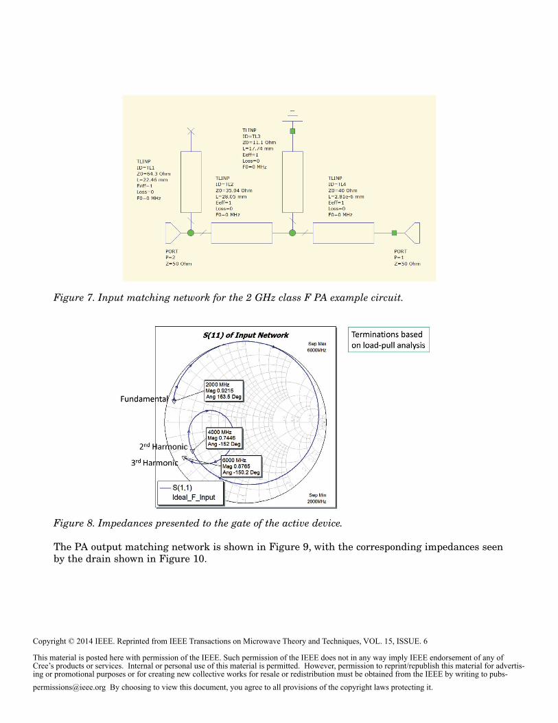
Using the input and output impedances determined by the above source- and load-pull simula-tions, matching networks were synthesized that corresponded closely with the required gate anddrain impedances at the fundamental and harmonics. The input network is shown in Figure 7.The transformed impedances presented at the Gan HEMT gate are shown in Figure 8.
This material is posted here with permission of the IEEE. Such permission of the IEEE does not in any way imply IEEE endorsement of any of Cree’s products or services. Internal or personal use of this material is permitted. However, permission to reprint/republish this material for advertis-ing or promotional purposes or for creating new collective works for resale or redistribution must be obtained from the IEEE by writing to [email protected] By choosing to view this document, you agree to all provisions of the copyright laws protecting it.
Figure 7. Input matching network for the 2 GHz class F PA example circuit.
Figure 8. Impedances presented to the gate of the active device.
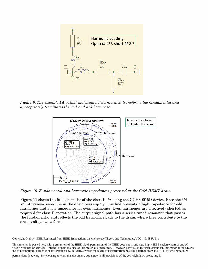
The PA output matching network is shown in Figure 9, with the corresponding impedances seenby the drain shown in Figure 10.
This material is posted here with permission of the IEEE. Such permission of the IEEE does not in any way imply IEEE endorsement of any of Cree’s products or services. Internal or personal use of this material is permitted. However, permission to reprint/republish this material for advertis-ing or promotional purposes or for creating new collective works for resale or redistribution must be obtained from the IEEE by writing to [email protected] By choosing to view this document, you agree to all provisions of the copyright laws protecting it.
Figure 9. The example PA output matching network, which transforms the fundamental andappropriately terminates the 2nd and 3rd harmonics.
Figure 10. Fundamental and harmonic impedances presented at the GaN HEMT drain.
Figure 11 shows the full schematic of the class F PA using the CGH60015D device. Note the λ/4shunt transmission line in the drain bias supply. This line presents a high impedance for oddharmonics and a low impedance for even harmonics. Even harmonics are effectively shorted, asrequired for class F operation. The output signal path has a series tuned resonator that passesthe fundamental and reflects the odd harmonics back to the drain, where they contribute to thedrain voltage waveform.
This material is posted here with permission of the IEEE. Such permission of the IEEE does not in any way imply IEEE endorsement of any of Cree’s products or services. Internal or personal use of this material is permitted. However, permission to reprint/republish this material for advertis-ing or promotional purposes or for creating new collective works for resale or redistribution must be obtained from the IEEE by writing to [email protected] By choosing to view this document, you agree to all provisions of the copyright laws protecting it.
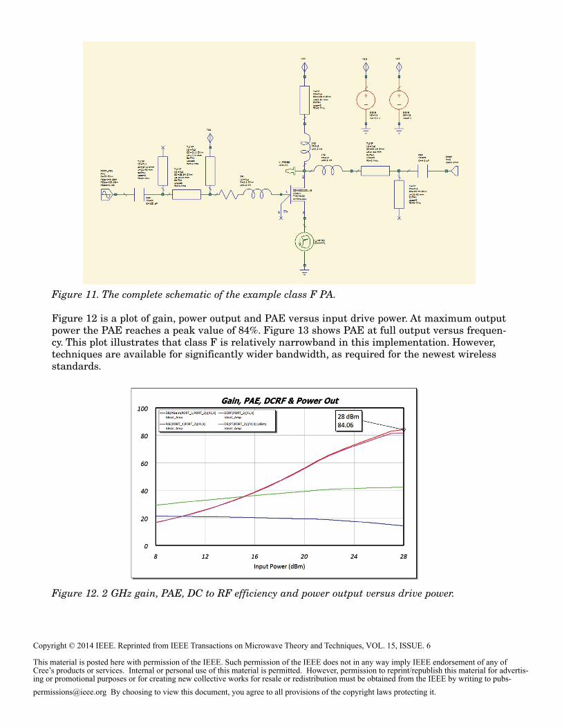
Figure 11. The complete schematic of the example class F PA.
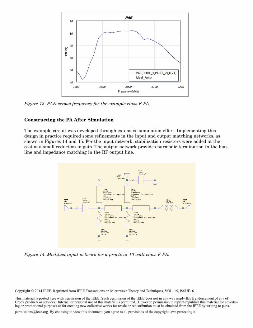
Figure 12 is a plot of gain, power output and PAE versus input drive power. At maximum outputpower the PAE reaches a peak value of 84%. Figure 13 shows PAE at full output versus frequen-cy. This plot illustrates that class F is relatively narrowband in this implementation. However,techniques are available for significantly wider bandwidth, as required for the newest wirelessstandards.
Figure 12. 2 GHz gain, PAE, DC to RF efficiency and power output versus drive power.
This material is posted here with permission of the IEEE. Such permission of the IEEE does not in any way imply IEEE endorsement of any of Cree’s products or services. Internal or personal use of this material is permitted. However, permission to reprint/republish this material for advertis-ing or promotional purposes or for creating new collective works for resale or redistribution must be obtained from the IEEE by writing to [email protected] By choosing to view this document, you agree to all provisions of the copyright laws protecting it.
Figure 13. PAE versus frequency for the example class F PA.
Constructing the PA After Simulation
The example circuit was developed through extensive simulation effort. Implementing thisdesign in practice required some refinements in the input and output matching networks, asshown in Figures 14 and 15. For the input network, stabilization resistors were added at thecost of a small reduction in gain. The output network provides harmonic termination in the biasline and impedance matching in the RF output line.
Figure 14. Modified input network for a practical 10 watt class F PA.
This material is posted here with permission of the IEEE. Such permission of the IEEE does not in any way imply IEEE endorsement of any of Cree’s products or services. Internal or personal use of this material is permitted. However, permission to reprint/republish this material for advertis-ing or promotional purposes or for creating new collective works for resale or redistribution must be obtained from the IEEE by writing to [email protected] By choosing to view this document, you agree to all provisions of the copyright laws protecting it.
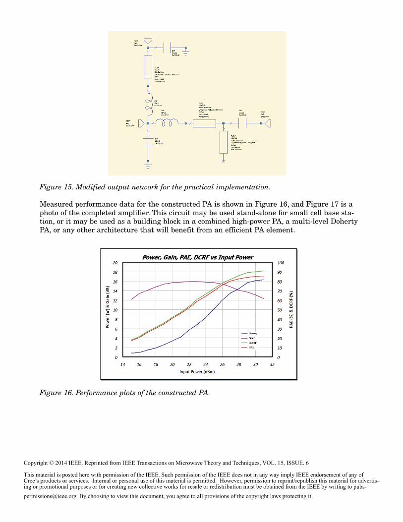
Figure 15. Modified output network for the practical implementation.
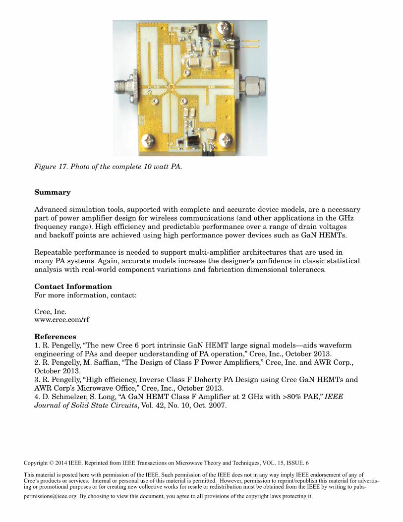
Measured performance data for the constructed PA is shown in Figure 16, and Figure 17 is aphoto of the completed amplifier. This circuit may be used stand-alone for small cell base sta-tion, or it may be used as a building block in a combined high-power PA, a multi-level DohertyPA, or any other architecture that will benefit from an efficient PA element.
Figure 16. Performance plots of the constructed PA.
This material is posted here with permission of the IEEE. Such permission of the IEEE does not in any way imply IEEE endorsement of any of Cree’s products or services. Internal or personal use of this material is permitted. However, permission to reprint/republish this material for advertis-ing or promotional purposes or for creating new collective works for resale or redistribution must be obtained from the IEEE by writing to [email protected] By choosing to view this document, you agree to all provisions of the copyright laws protecting it.
Figure 17. Photo of the complete 10 watt PA.
Summary
Advanced simulation tools, supported with complete and accurate device models, are a necessarypart of power amplifier design for wireless communications (and other applications in the GHzfrequency range). High efficiency and predictable performance over a range of drain voltagesand backoff points are achieved using high performance power devices such as GaN HEMTs.
Repeatable performance is needed to support multi-amplifier architectures that are used inmany PA systems. Again, accurate models increase the designer’s confidence in classic statisticalanalysis with real-world component variations and fabrication dimensional tolerances.
Contact InformationFor more information, contact:
Cree, Inc.www.cree.com/rf
References1. R. Pengelly, “The new Cree 6 port intrinsic GaN HEMT large signal models—aids waveformengineering of PAs and deeper understanding of PA operation,” Cree, Inc., October 2013.2. R. Pengelly, M. Saffian, “The Design of Class F Power Amplifiers,” Cree, Inc. and AWR Corp.,October 2013.3. R. Pengelly, “High efficiency, Inverse Class F Doherty PA Design using Cree GaN HEMTs andAWR Corp’s Microwave Office,” Cree, Inc., October 2013.4. D. Schmelzer, S. Long, “A GaN HEMT Class F Amplifier at 2 GHz with >80% PAE,” IEEEJournal of Solid State Circuits, Vol. 42, No. 10, Oct. 2007.