• Review (of Lecture 1 and Recitation 2) Carrier concentrations in TE given the doping level What happens above and below room temperature?
• Uniform excitation of uniform samples: drift (introduced in Rec. 2) Drift motion: carrier velocity verses fieldMobility, Drift currents, ConductivityImpact of temperature on mobility, conductivityIntegrated circuit resistors
• Uniform excitation: optical generationGeneration/recombination in TE Uniform optical generation - external excitation Population excesses, p¢ and n¢, and their transients Low level injection; minority carrier lifetime
• Uniform excitation - applied field and optical generationPhotoconductivity, photoconductors
Clif Fonstad, 9/03 Lecture 2 - Slide 1
Variation of carrier concentration with temperature
• Around R.T.Full ionization Extrinsic doping
-Nd + ª Nd , Na ª Na + (Nd - Na ) >> ni
2n ª (Nd - Na ), po = ni no
• At very high TFull ionization Intrinsic behavior
-Nd + ª Nd , Na ª Na
+ ni >> Nd - Na no ª po ª ni
• At very low T
(Note: for convenience we assume an n-type sample)
o
Nd + << Nd - type( )assuming n + Incomplete ionization Nd - N >> niaExtrinsic doping, but
+ 2with carrier freeze-out n ª (Nd - Na ) << (Nd - Na ), po = ni no o Clif Fonstad, 9/03 Lecture 2 - Slide 2
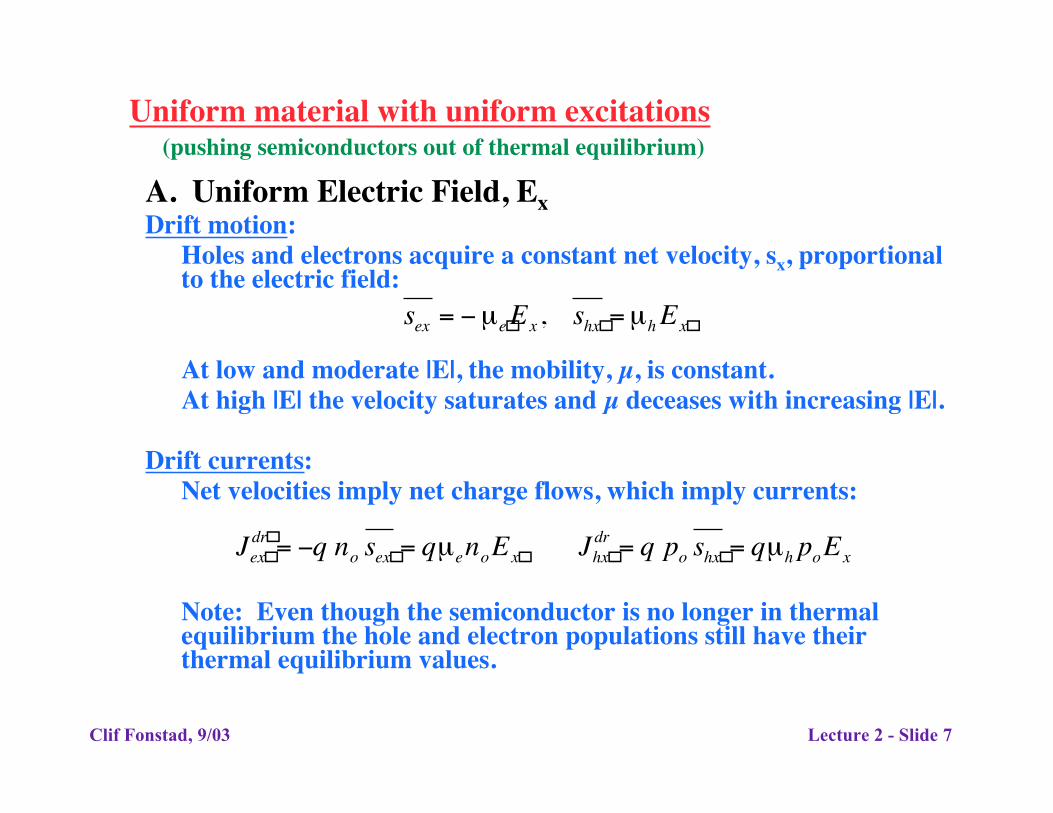
Uniform material with uniform excitations(pushing semiconductors out of thermal equilibrium)
A. Uniform Electric Field, Ex Drift motion:
Holes and electrons acquire a constant net velocity, sx, proportional to the electric field:
No field E-field applied
sex e Ex, shx =mhEx Ex= -m
At low and moderate |E|, the mobility, µ, is constant.At high |E| the velocity saturates and µ deceases with increasing |E|.
Clif Fonstad, 9/03 Lecture 2 - Slide 3
Velocity saturationThe breakdown of Ohm's law at large electric fields.
See Fig 5.7, from Neamen, D. Electronic Circuit Analysis and Design. McGraw-Hill Higher Education, 1996.
Above: Velocity vs. field plot at R.T. for holes and electrons in Si (loglog plot). (Fonstad, Fig. 3.2)
Left: Velocity-field curves for Si, Ge, and GaAs at R.T. (log-log plot). (Neaman, Fig. 5.7)
Clif Fonstad, 9/03 Lecture 2 - Slide 4
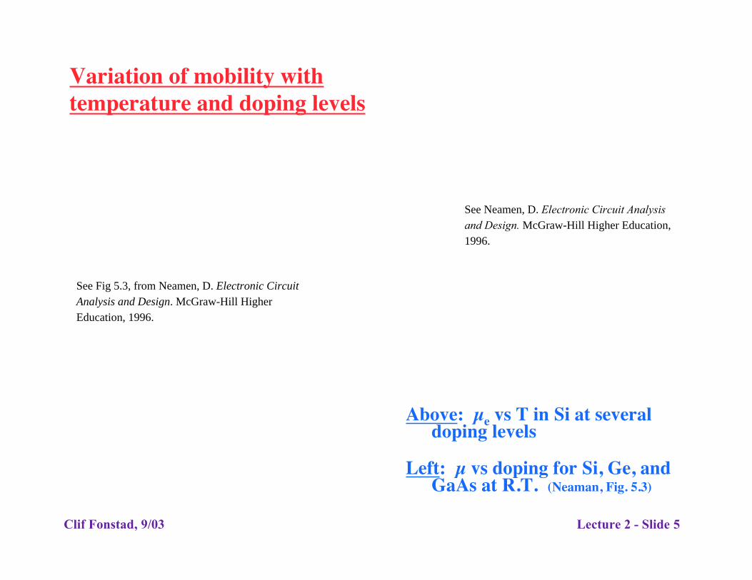
Variation of mobility with temperature and doping levels
See Neamen, D. Electronic Circuit Analysis and Design. McGraw-Hill Higher Education, 1996.
See Fig 5.3, from Neamen, D. Electronic Circuit Analysis and Design. McGraw-Hill Higher Education, 1996.
Above: µe vs T in Si at several doping levels
Left: µ vs doping for Si, Ge, and GaAs at R.T. (Neaman, Fig. 5.3)
Clif Fonstad, 9/03 Lecture 2 - Slide 5
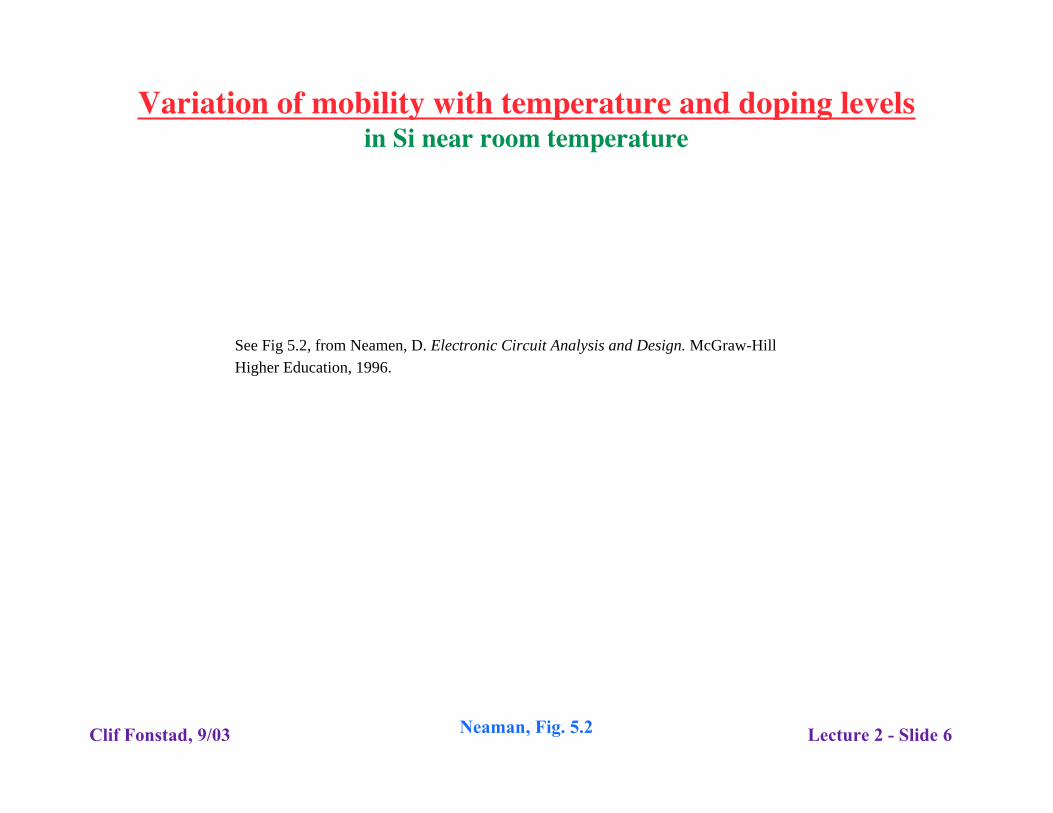
Variation of mobility with temperature and doping levelsin Si near room temperature
See Fig 5.2, from Neamen, D. Electronic Circuit Analysis and Design. McGraw-Hill Higher Education, 1996.
Uniform material with uniform excitations(pushing semiconductors out of thermal equilibrium)
A. Uniform Electric Field, Ex Drift motion:
Holes and electrons acquire a constant net velocity, sx, proportional to the electric field:
s = -m Ex, shx =mhEex e x
At low and moderate |E|, the mobility, µ, is constant.At high |E| the velocity saturates and µ deceases with increasing |E|.
Drift currents:Net velocities imply net charge flows, which imply currents:
drJ dr = -q no s = qmenoEx Jhx = q po shx = qmh poExex ex
Note: Even though the semiconductor is no longer in thermal equilibrium the hole and electron populations still have their thermal equilibrium values.
Clif Fonstad, 9/03 Lecture 2 - Slide 7
Conductivity, so: Ohm's law on a microscale states that the drift current density is linearly proportional to the electric field:
Jdr =s Ex o x
The total drift current is the sum of the hole and electron drift currents. Using our early expressions we find:
dr = JdrJxdr
ex + Jhx = qm n E + qmh poE = q(m n +mh po)Ee o x x e o x
From this we see obtain our expression for the conductivity: s = q(m n +mh po) [S/cm]o e o
Majority vs. minority carriers: Drift and conductivity are dominated by the most numerous, or "majority," carriers:
n-type n >> po fis ª qm no o e o
p-type po >> n fis o ª qmh poo
Clif Fonstad, 9/03 Lecture 2 - Slide 8
Resistance, R, and resistivity, ro: Ohm's law on a macroscopic scale says that the current and voltage are linearly related: vab = R iD
l
w
iD
vAB
so
The question is, "What is R?" t JdrWe have: =s Ex o x
iDwith E = vAB and Jdr = x l x w ⋅ t
Combining these we find: iD vAB +
=sw ⋅ t o l l 1
which yields: vAB = iD = R iD w ⋅ t s o lwhere R ≡
l 1 = r
w ⋅ t s w ⋅ t o o
Note: Resistivity, ro, is defined as the inverse of the conductivity: ≡ 1
sr [Ohm - cm] o o
Clif Fonstad, 9/03 Lecture 2 - Slide 9
Integrated resistors Our first device!!
Courtesy of Fairchild Semiconductor. Used with permission.
Diffused resistors: High sheet resistance semiconductor patterns (pink) with low resistance Al (white) "wires" contacting each end.
Thin-film resistors: High sheet resistance tantalum films (green)with low resistance Al (white) "wires" contacting each end.Clif Fonstad, 9/03 Lecture 2 - Slide 10
cc_rchakr
Text Box
(Courtesy of Fairchild Semiconductor Corporation. Fairchild Semiconductor, A Solid State of Progress, 1964.)
Uniform material with uniform excitations(pushing semiconductors out of thermal equilibrium)
B. Uniform Optical Generation, gL (t)Generation, G, and recombination, R:
If G > R, the populations are increasingdn dpG > R fi = > 0 dt dt
If G < R, the populations are decreasing dn dpG < R fi = < 0 dt dt
In general dn dp= = G - R
dt dt Optical generation, gL(t):
In thermal equilibrium, G = R = no po r(T)o o
With gL(t): G = G + gL (t)o R = n p r(T) = (no + n')(po + p') r(T)
Clif Fonstad, 9/03 Lecture 2 - Slide 11
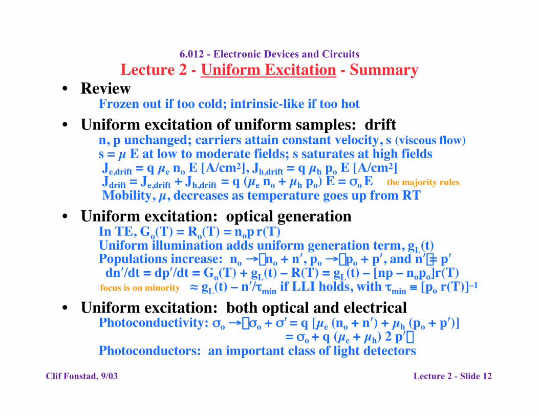
6.012 - Electronic Devices and Circuits
Lecture 2 - Uniform Excitation - Summary• Review
Frozen out if too cold; intrinsic-like if too hot • Uniform excitation of uniform samples: drift
n, p unchanged; carriers attain constant velocity, s (viscous flow)
JJ
s = µ E at low to moderate fields; s saturates at high fields e,drift = q µe no E [A/cm2], Jh,drift = q µh po E [A/cm2] drift = Je,drift + Jh,drift = q (µe no + µh po) E = so E the majority rules
Mobility, µ, decreases as temperature goes up from RT • Uniform excitation: optical generation
In TE, Go(T) = Ro(T) = nop r(T) Uniform illumination adds uniform generation term, gL(t)Populations increase: no Æ no + n¢, po Æ po + p¢, and n¢ = p¢
dn¢/dt = dp¢/dt = Go(T) + gL(t) – R(T) = gL(t) – [np – nopo]r(T)focus is on minority ≈ gL(t) – n¢/tmin if LLI holds, with tmin ≡ [po r(T)]–1
• Uniform excitation: both optical and electricalPhotoconductivity: so Æ so + s¢= q [µe (no + n¢) + µh (po + p¢)]
= so + q (µe + µh) 2 p¢ Photoconductors: an important class of light detectors