47
Interface 8088 I/F with basic IO, RAM and 8255
| Date post: | 06-Apr-2018 |
| Category: |
Documents |
| Upload: | ammar-ishaqui |
| View: | 220 times |
| Download: | 0 times |
8/3/2019 6.1 Basic Interface
http://slidepdf.com/reader/full/61-basic-interface 1/47
Interface 8088 I/F with basic IO, RAM
and 8255
8/3/2019 6.1 Basic Interface
http://slidepdf.com/reader/full/61-basic-interface 2/47
Topics Timing diagram
• Address Bus, R/W, Data
• Memory Map I/O
Address Decoding
• CPU is addressable lager than devices.
Chip Supports• TTL : De-multiplexer, Latch, Buffer
8/3/2019 6.1 Basic Interface
http://slidepdf.com/reader/full/61-basic-interface 3/47
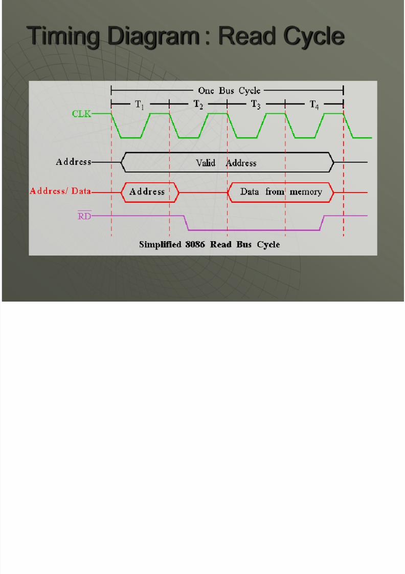
Timing Diagram : Read Cycle

8/3/2019 6.1 Basic Interface
http://slidepdf.com/reader/full/61-basic-interface 4/47
Timing Diagram : Write Cycle
8/3/2019 6.1 Basic Interface
http://slidepdf.com/reader/full/61-basic-interface 5/47
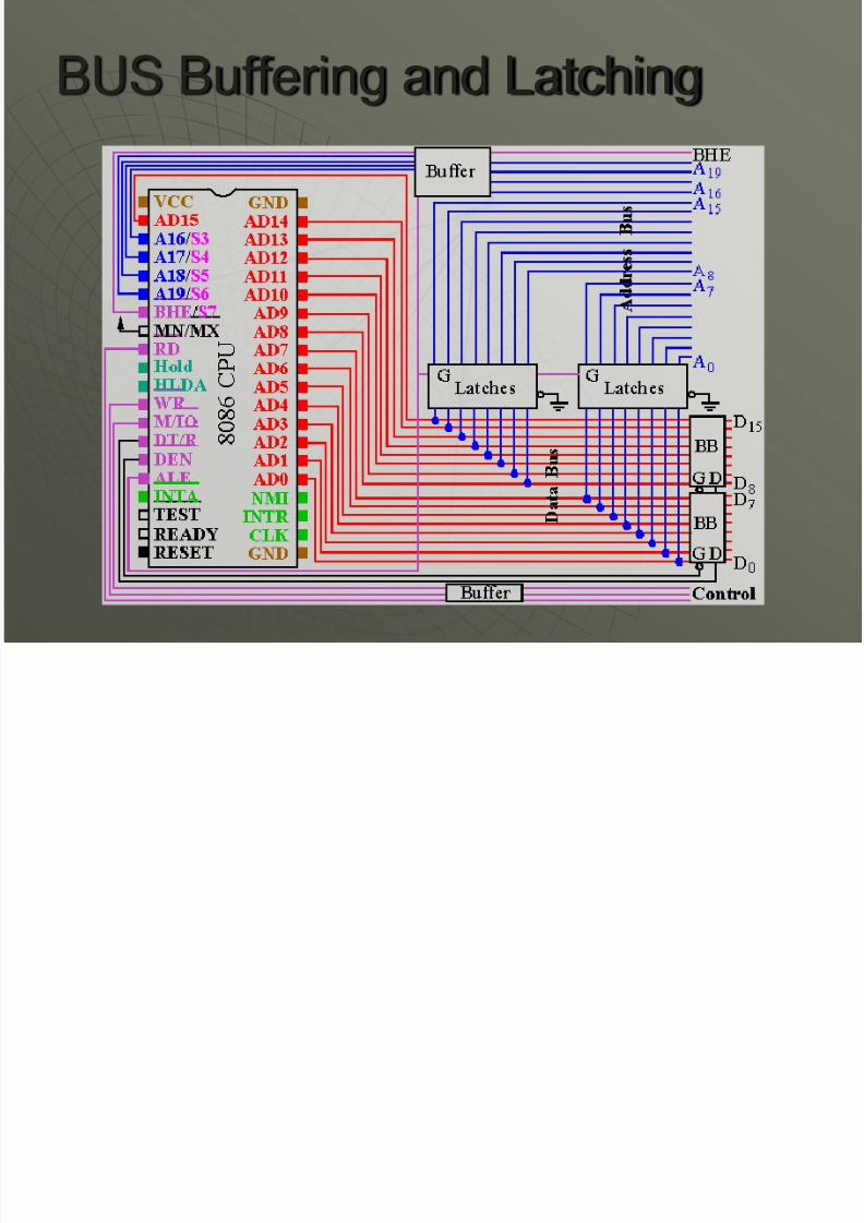
BUS Buffering and Latching
8/3/2019 6.1 Basic Interface
http://slidepdf.com/reader/full/61-basic-interface 6/47
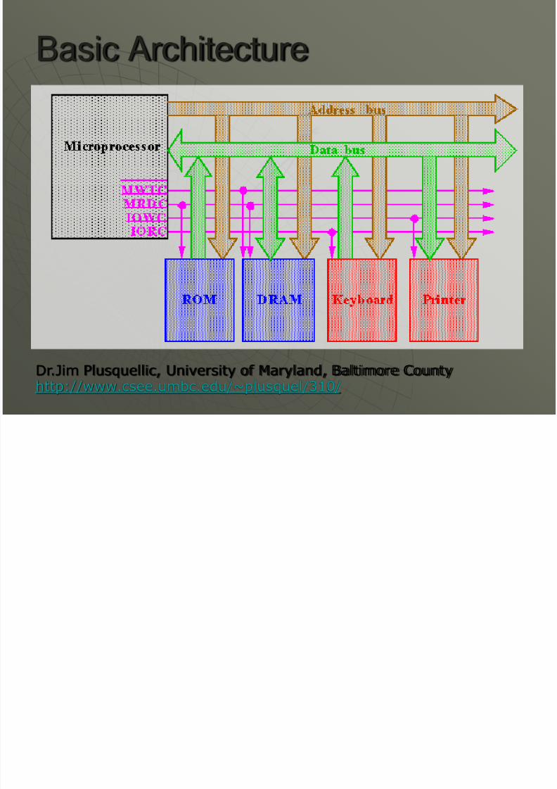
Basic Architecture
Dr.Jim Plusquellic, University of Maryland, Baltimore County
http://www.csee.umbc.edu/~plusquel/310/
8/3/2019 6.1 Basic Interface
http://slidepdf.com/reader/full/61-basic-interface 7/47
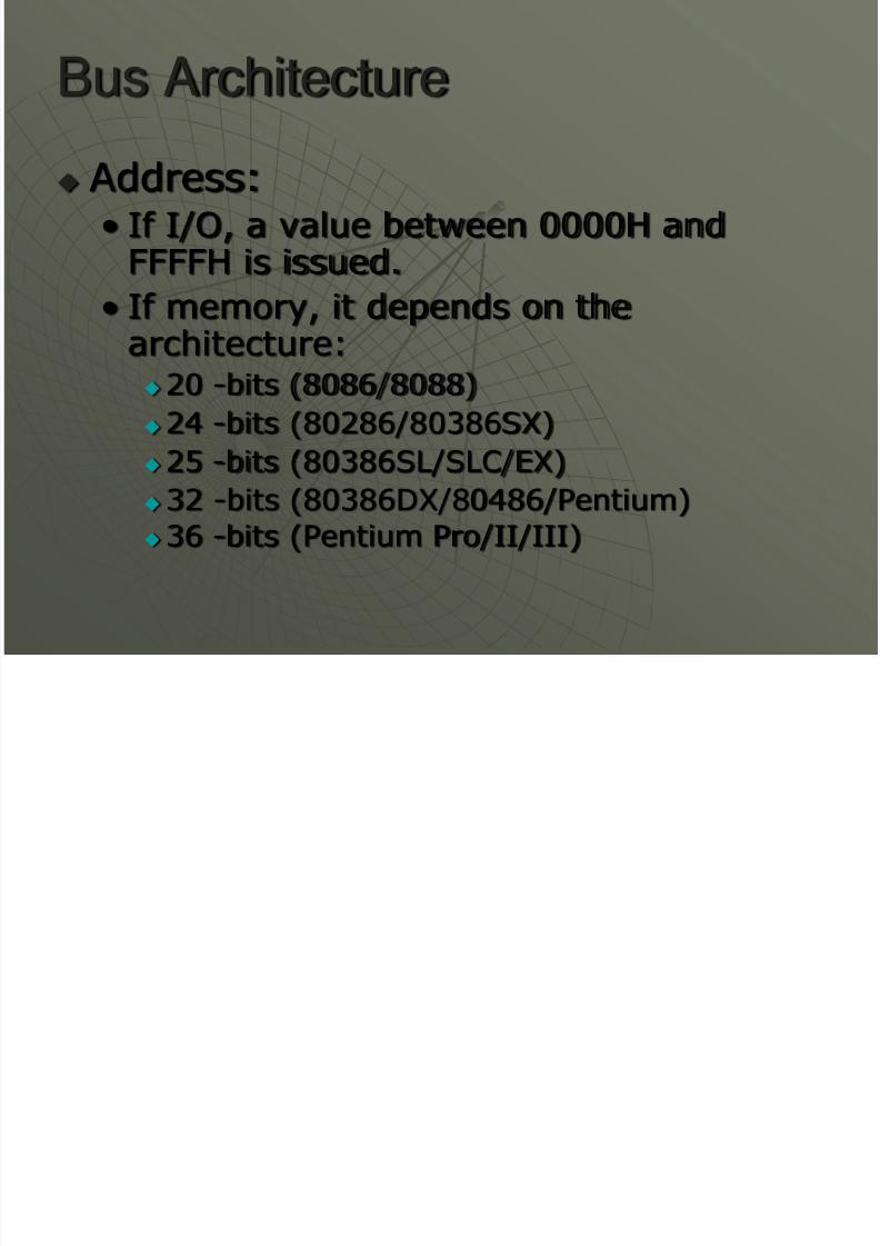
Bus Architecture Address:
• If I/O, a value between 0000H andFFFFH is issued.
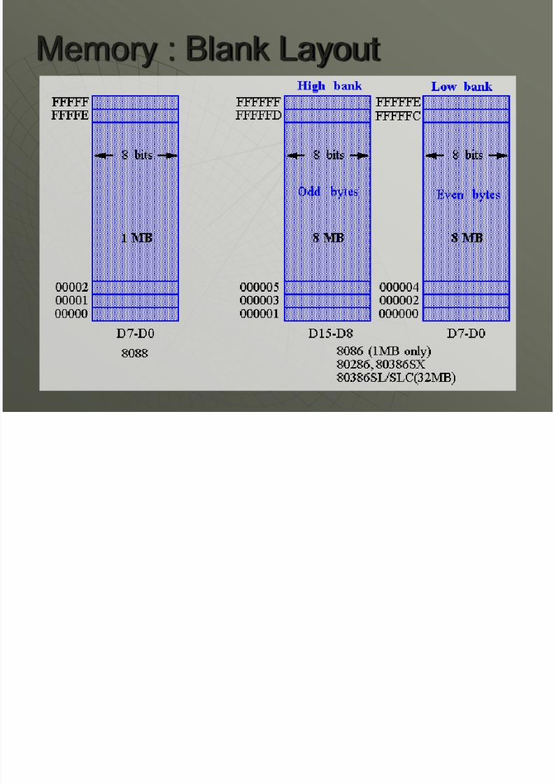
• If memory, it depends on thearchitecture:20 -bits (8086/8088)
24 -bits (80286/80386SX)
25 -bits (80386SL/SLC/EX)32 -bits (80386DX/80486/Pentium)
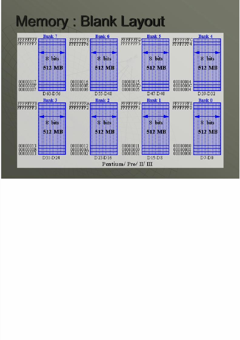
36 -bits (Pentium Pro/II/III)
8/3/2019 6.1 Basic Interface
http://slidepdf.com/reader/full/61-basic-interface 8/47
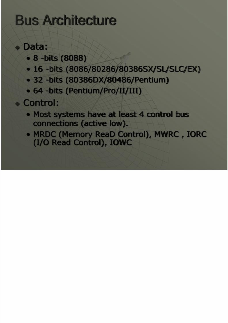
Bus Architecture Data:
• 8 -bits (8088)
• 16 -bits (8086/80286/80386SX/SL/SLC/EX)
• 32 -bits (80386DX/80486/Pentium)• 64 -bits (Pentium/Pro/II/III)
Control:
• Most systems have at least 4 control busconnections (active low).
• MRDC (Memory ReaD Control), MWRC , IORC(I/O Read Control), IOWC
8/3/2019 6.1 Basic Interface
http://slidepdf.com/reader/full/61-basic-interface 9/47
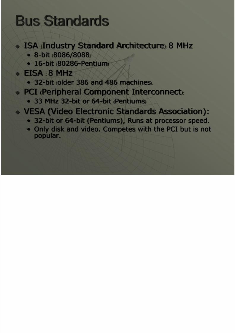
Bus Standards ISA (Industry Standard Architecture): 8 MHz
• 8-bit (8086/8088)
• 16-bit (80286-Pentium)
EISA : 8 MHz
• 32-bit (older 386 and 486 machines).
PCI (Peripheral Component Interconnect):
• 33 MHz 32-bit or 64-bit (Pentiums) VESA (Video Electronic Standards Association):
•
32-bit or 64-bit (Pentiums), Runs at processor speed.• Only disk and video. Competes with the PCI but is not
popular.
8/3/2019 6.1 Basic Interface
http://slidepdf.com/reader/full/61-basic-interface 10/47
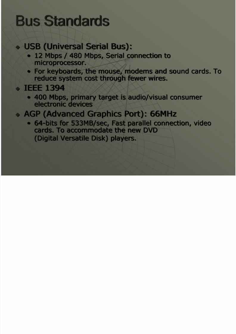
Bus Standards USB (Universal Serial Bus):
• 12 Mbps / 480 Mbps, Serial connection tomicroprocessor.
• For keyboards, the mouse, modems and sound cards. Toreduce system cost through fewer wires.
IEEE 1394• 400 Mbps, primary target is audio/visual consumer
electronic devices
AGP (Advanced Graphics Port): 66MHz
• 64-bits for 533MB/sec, Fast parallel connection, videocards. To accommodate the new DVD
(Digital Versatile Disk) players.
8/3/2019 6.1 Basic Interface
http://slidepdf.com/reader/full/61-basic-interface 11/47
Memory : Blank Layout

8/3/2019 6.1 Basic Interface
http://slidepdf.com/reader/full/61-basic-interface 12/47
Memory : Blank Layout
8/3/2019 6.1 Basic Interface
http://slidepdf.com/reader/full/61-basic-interface 13/47
Memory : Blank Layout
8/3/2019 6.1 Basic Interface
http://slidepdf.com/reader/full/61-basic-interface 14/47
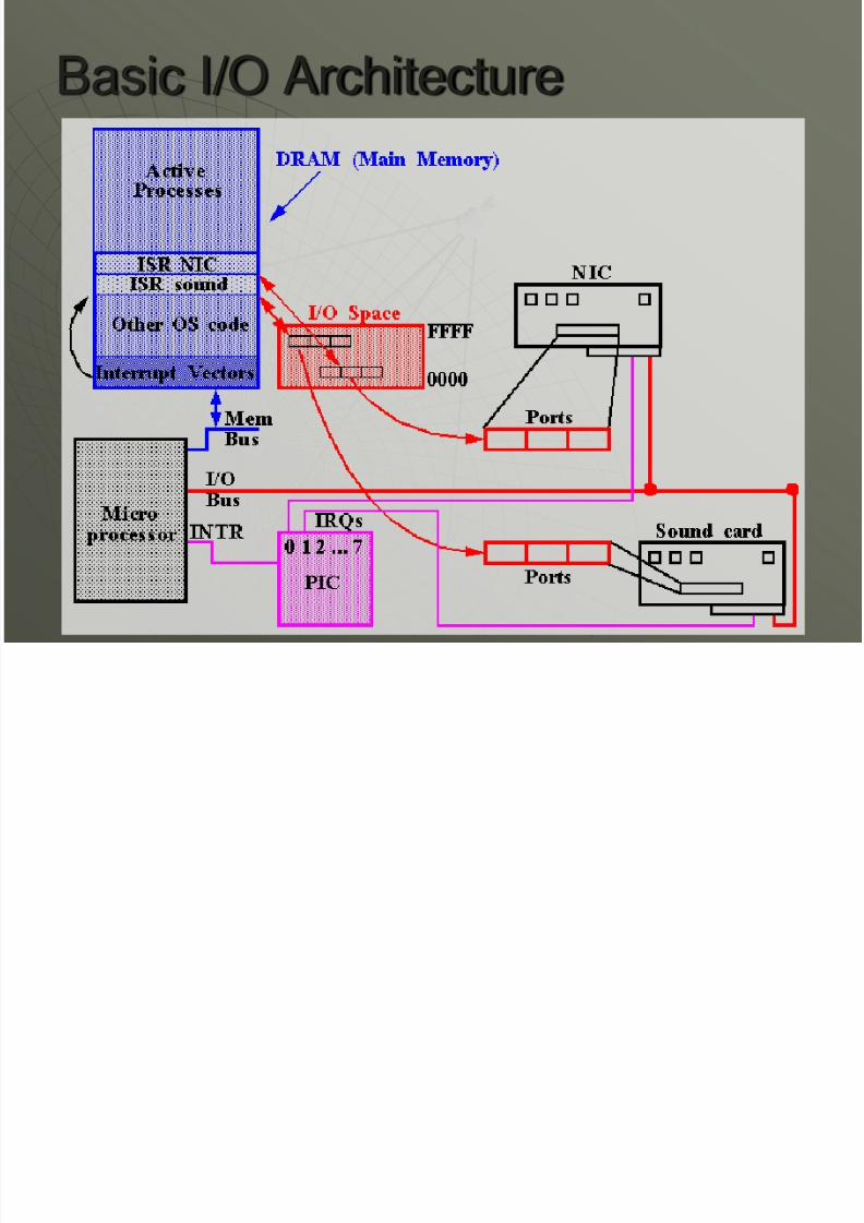
Basic I/O Architecture
8/3/2019 6.1 Basic Interface
http://slidepdf.com/reader/full/61-basic-interface 15/47
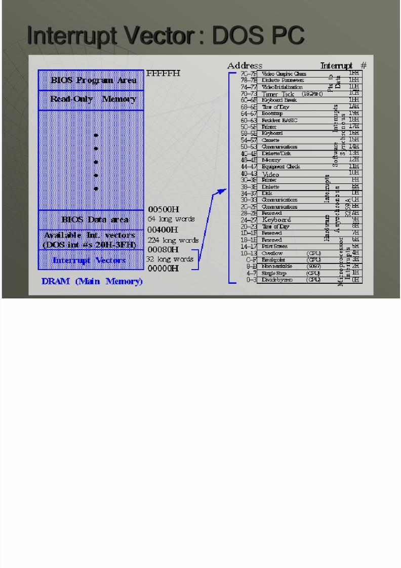
Interrupt Vector : DOS PC

8/3/2019 6.1 Basic Interface
http://slidepdf.com/reader/full/61-basic-interface 16/47
IO Space
8/3/2019 6.1 Basic Interface
http://slidepdf.com/reader/full/61-basic-interface 17/47
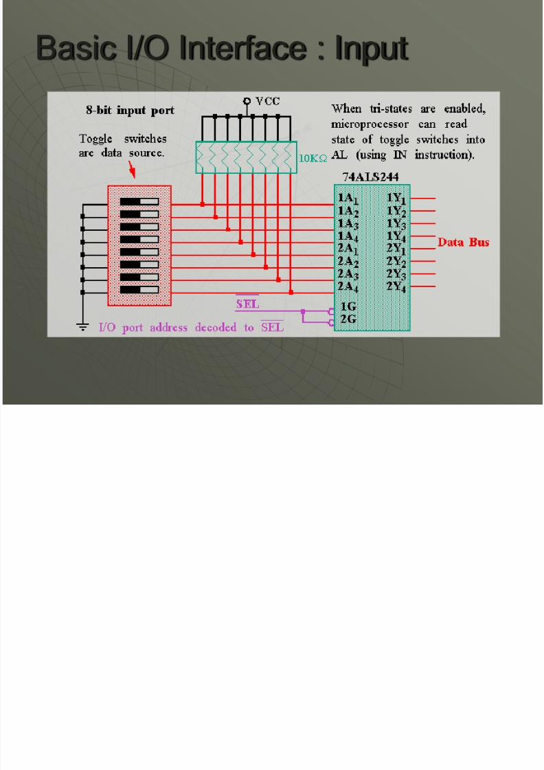
Basic I/O Interface : Input

8/3/2019 6.1 Basic Interface
http://slidepdf.com/reader/full/61-basic-interface 18/47
Basic I/O Interface : Output

8/3/2019 6.1 Basic Interface
http://slidepdf.com/reader/full/61-basic-interface 19/47
I/O Port Decoding
8/3/2019 6.1 Basic Interface
http://slidepdf.com/reader/full/61-basic-interface 20/47
MEMORY
8/3/2019 6.1 Basic Interface
http://slidepdf.com/reader/full/61-basic-interface 21/47
Memory Types Two basic types:
• ROM: Read-only memory
• RAM: Read-Write memory
Four commonly used memories:
• ROM
• Flash (EEPROM)
• Static RAM (SRAM)
• Dynamic RAM (DRAM)

8/3/2019 6.1 Basic Interface
http://slidepdf.com/reader/full/61-basic-interface 22/47
Memory Chips The data pins are typically bi-directional in
read-write memories.• The number of data pins is related to the size
of the memory location. For example, an 8-bit
wide (byte-wide) memory device has 8 datapins.
Each memory device has at least one chipselect (CS) or chip enable (CE) or select(S) pin that enables the memory device.• This enables read and/or write operations.• If more than one are present, then all must be
0 in order to perform a read or write.
8/3/2019 6.1 Basic Interface
http://slidepdf.com/reader/full/61-basic-interface 23/47
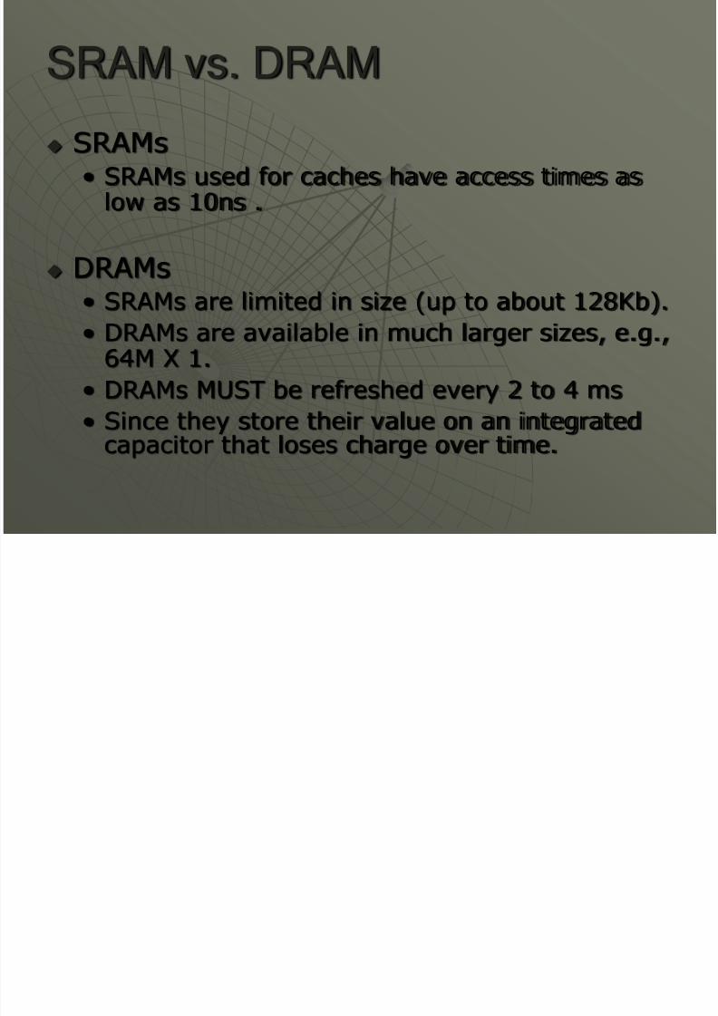
SRAM vs. DRAM SRAMs
• SRAMs used for caches have access times aslow as 10ns .
DRAMs• SRAMs are limited in size (up to about 128Kb).
• DRAMs are available in much larger sizes, e.g.,64M X 1.
• DRAMs MUST be refreshed every 2 to 4 ms
• Since they store their value on an integratedcapacitor that loses charge over time.

8/3/2019 6.1 Basic Interface
http://slidepdf.com/reader/full/61-basic-interface 24/47
Memory Address
Decoding

8/3/2019 6.1 Basic Interface
http://slidepdf.com/reader/full/61-basic-interface 25/47
Memory Address Decoding The processor can usually address a
memory space that is much largerthan the memory space covered by
an individual memory chip. In order to splice a memory device
into the address space of theprocessor, decoding is necessary.
For example, the 8088 issues 20-bitaddresses for a total of 1MB of memory address space.
8/3/2019 6.1 Basic Interface
http://slidepdf.com/reader/full/61-basic-interface 26/47
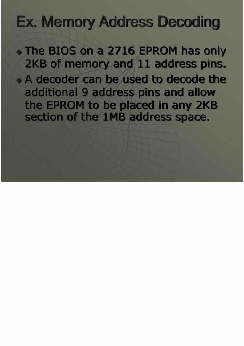
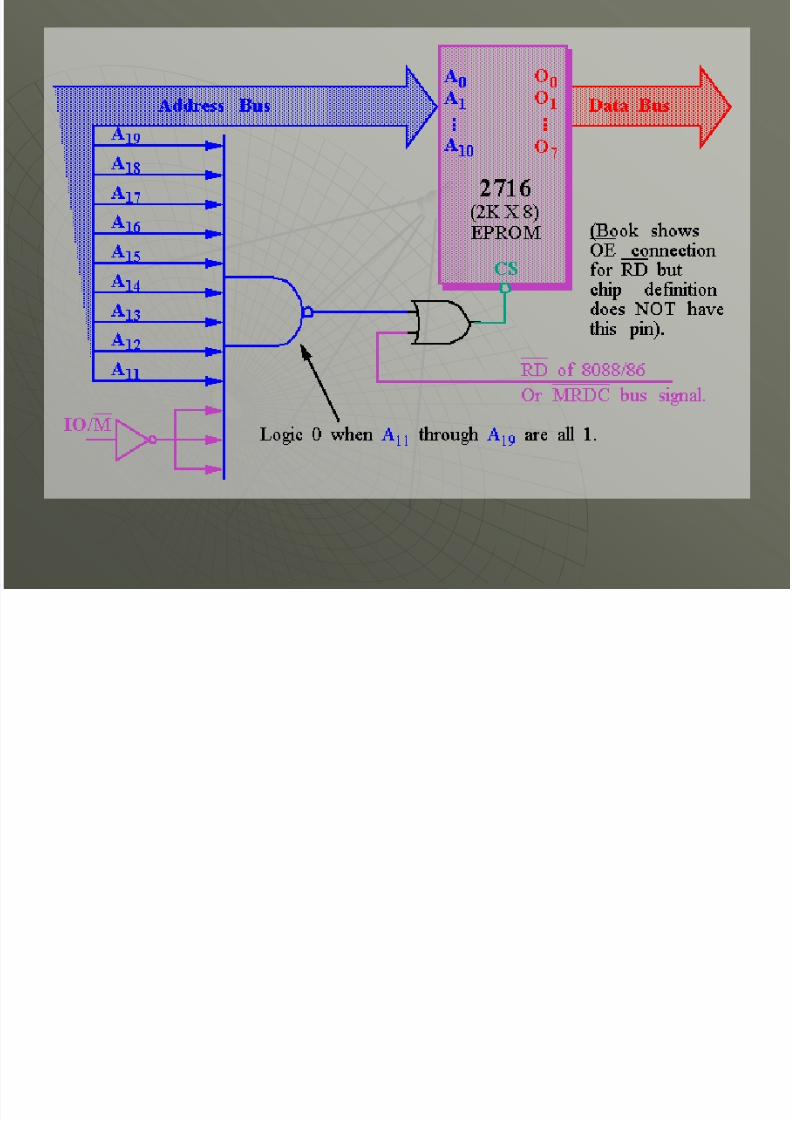
Ex. Memory Address Decoding The BIOS on a 2716 EPROM has only
2KB of memory and 11 address pins.
A decoder can be used to decode theadditional 9 address pins and allowthe EPROM to be placed in any 2KBsection of the 1MB address space.
8/3/2019 6.1 Basic Interface
http://slidepdf.com/reader/full/61-basic-interface 27/47

8/3/2019 6.1 Basic Interface
http://slidepdf.com/reader/full/61-basic-interface 28/47
Ex. Memory Address Decoding To determine the address range that a
device is mapped into:

8/3/2019 6.1 Basic Interface
http://slidepdf.com/reader/full/61-basic-interface 29/47
Ex. Memory Address Decoding This 2KB memory segment maps into
the reset location of the 8086/8088(FFFF0H).
NAND gate decoders are not oftenused. Rather the 3-to-8 Line Decoder
(74LS138) is more common.

8/3/2019 6.1 Basic Interface
http://slidepdf.com/reader/full/61-basic-interface 30/47
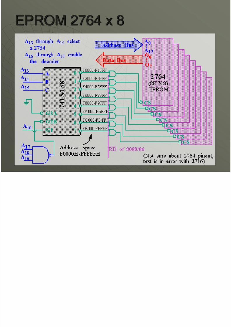
3-to-8 Line Decoder
G2A, G2B, and G1 must be active.
Each output of the decoder can be attached to an2764 EPROM ( 8K X 8 ).
8/3/2019 6.1 Basic Interface
http://slidepdf.com/reader/full/61-basic-interface 31/47
EPROM 2764 x 8

8/3/2019 6.1 Basic Interface
http://slidepdf.com/reader/full/61-basic-interface 32/47

8/3/2019 6.1 Basic Interface
http://slidepdf.com/reader/full/61-basic-interface 33/47
More on Address Decoding Yet a third possibility is a PLD
(Programmable Logic Device).
• PLDs come in three varieties:
• PLA (Programmable Logic Array)
• PAL (Programmable Array Logic)
• GAL (Gated Array Logic)
A PAL example (16L8) is commonly used to decode thememory address, particularly for 32-bit addressesgenerated by the 80386DX and above.
8/3/2019 6.1 Basic Interface
http://slidepdf.com/reader/full/61-basic-interface 34/47
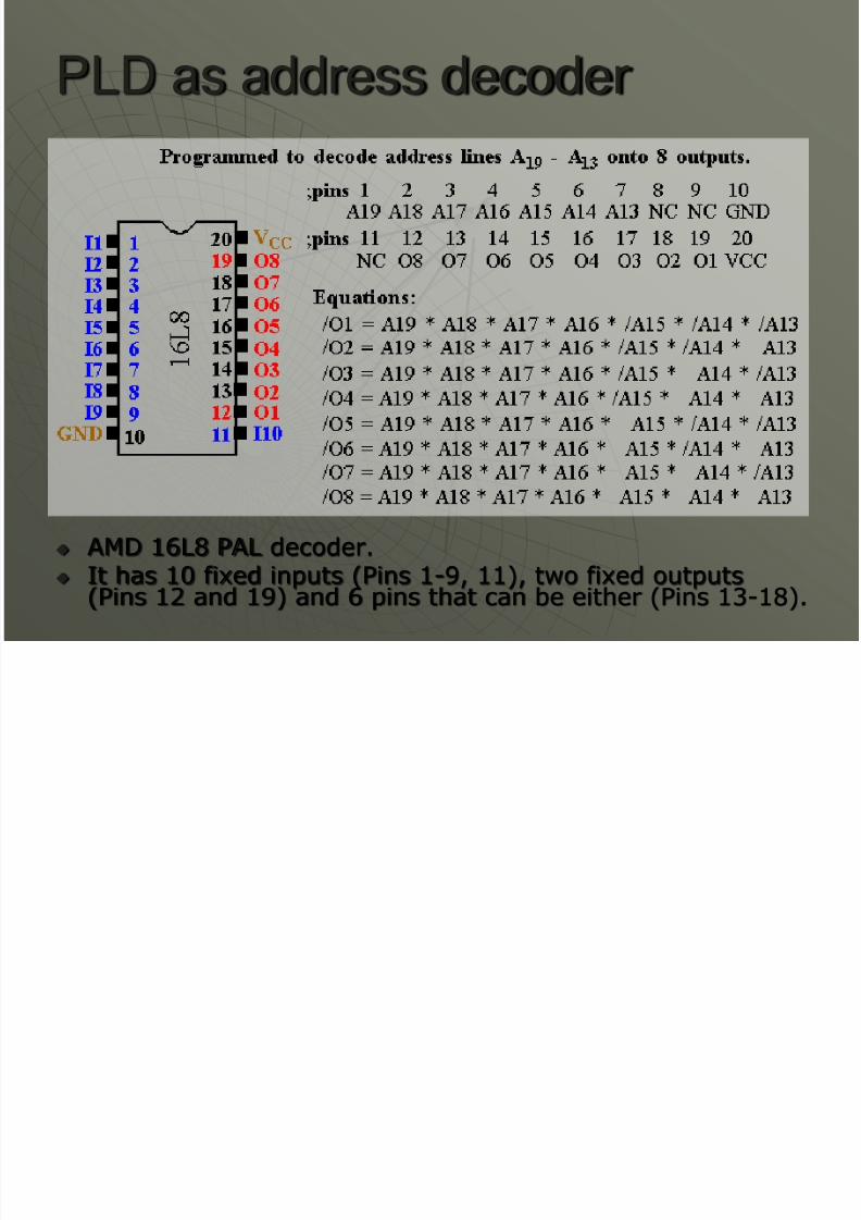
PLD as address decoder
AMD 16L8 PAL decoder. It has 10 fixed inputs (Pins 1-9, 11), two fixed outputs
(Pins 12 and 19) and 6 pins that can be either (Pins 13-18).
8/3/2019 6.1 Basic Interface
http://slidepdf.com/reader/full/61-basic-interface 35/47
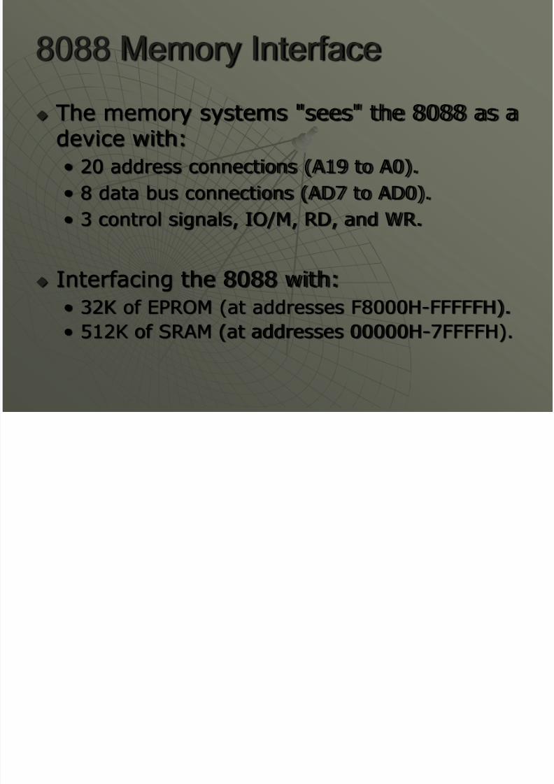
8088 Memory Interface The memory systems "sees" the 8088 as a
device with:
• 20 address connections (A19 to A0).
•
8 data bus connections (AD7 to AD0).• 3 control signals, IO/M, RD, and WR.
Interfacing the 8088 with:
• 32K of EPROM (at addresses F8000H-FFFFFH).
• 512K of SRAM (at addresses 00000H-7FFFFH).

8/3/2019 6.1 Basic Interface
http://slidepdf.com/reader/full/61-basic-interface 36/47
8088 Memory Interface: EPROM

8/3/2019 6.1 Basic Interface
http://slidepdf.com/reader/full/61-basic-interface 37/47
8088 Memory Interface: EPROM The EPROM will also require the
generation of a wait state.
• The EPROM has an access time of 450ns .
•
The 74LS138 requires 12ns to decode.
The 8088 runs at 5MHz and only allows460ns for memory to access data.
A wait state adds 200ns of additional time
8/3/2019 6.1 Basic Interface
http://slidepdf.com/reader/full/61-basic-interface 38/47
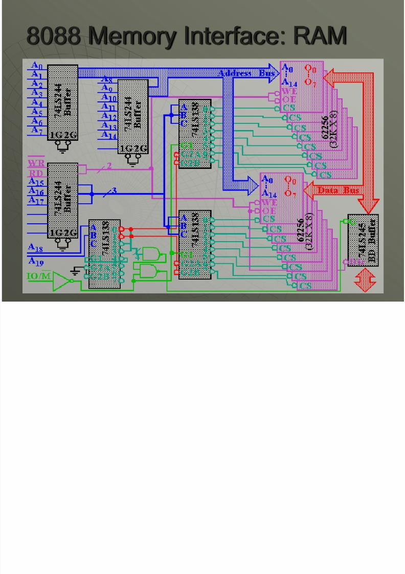
8088 Memory Interface: RAM

8/3/2019 6.1 Basic Interface
http://slidepdf.com/reader/full/61-basic-interface 39/47
8088 Memory Interface: RAM The 62256s on the previous slide are
actually SRAMs. Access times are onorder of 10ns .
Flash memory can also be interfacedto the 8088. However, the write time
( 400ms !) is too slow to be used asRAM.

8/3/2019 6.1 Basic Interface
http://slidepdf.com/reader/full/61-basic-interface 40/47
8088 I/F withProgrammable Peripheral
Interface 8255 Part I
8/3/2019 6.1 Basic Interface
http://slidepdf.com/reader/full/61-basic-interface 41/47

8/3/2019 6.1 Basic Interface
http://slidepdf.com/reader/full/61-basic-interface 42/47
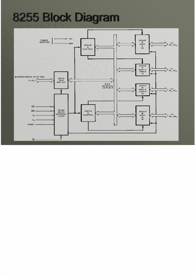
PPI : 82C55 The 82C55 is a popular interfacing component,
that can interface any TTL-compatible I/O deviceto the microprocessor.
It is used to interface to the keyboard and aparallel printer port in PCs (usually as part of an
integrated chipset). Requires insertion of wait states if used with a
microprocessor using higher that an 8 MHz clock. PPI has 24 pins for I/O that are programmable in
groups of 12 pins and has three distinct modes of
operation. In the PC, an 82C55 or its equivalent is decoded
at I/O ports 60H-63H.
8/3/2019 6.1 Basic Interface
http://slidepdf.com/reader/full/61-basic-interface 43/47
8255 Block Diagram

8/3/2019 6.1 Basic Interface
http://slidepdf.com/reader/full/61-basic-interface 44/47
Pin layout of 8255
8/3/2019 6.1 Basic Interface
http://slidepdf.com/reader/full/61-basic-interface 45/47
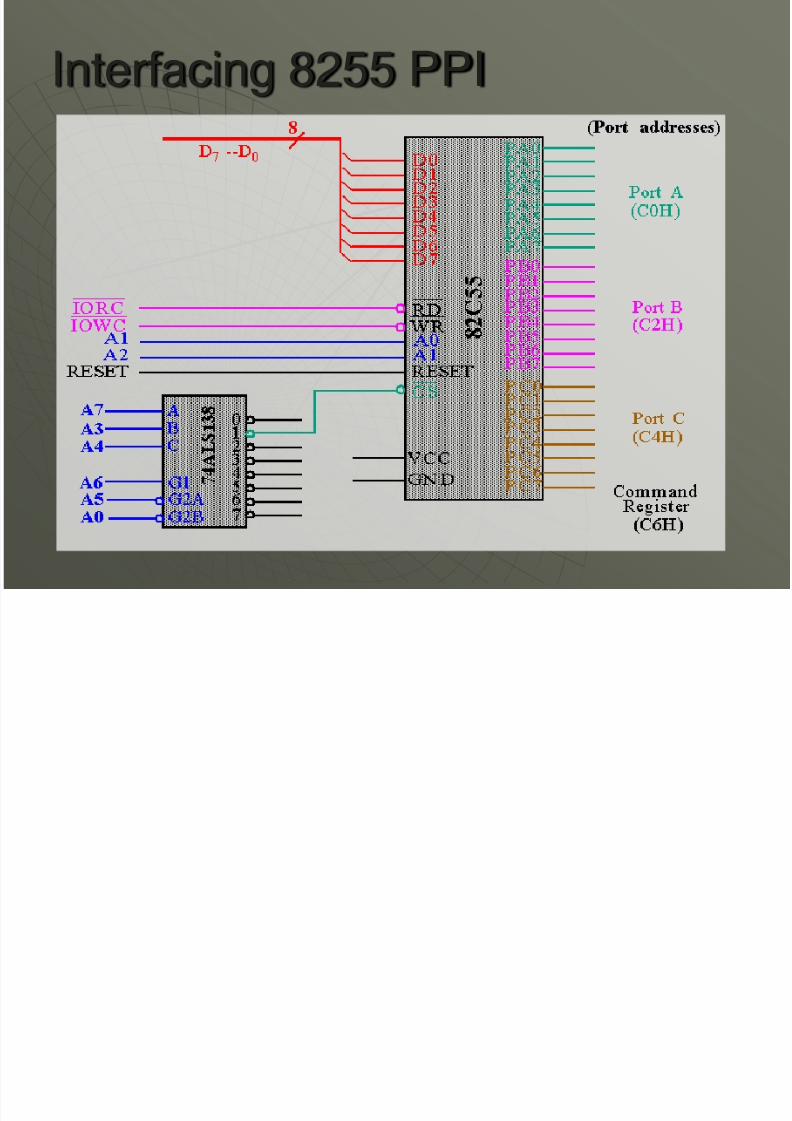
Interfacing 8255 PPI

8/3/2019 6.1 Basic Interface
http://slidepdf.com/reader/full/61-basic-interface 46/47
8/3/2019 6.1 Basic Interface
http://slidepdf.com/reader/full/61-basic-interface 47/47
That’s all


