A STUDY OF ADDERS A STUDY OF ADDERS B.Tech Project Report Submitted towards partial fulfillment of the requirement for the Degree of B.TECH IN ELECTRONICS & COMMUNICATION ENGINEERING By Anirban Banerjee Registration No: 071270103101029 Roll No: 071270103029 Under the supervision of Mr. Saradindu Panda Department of Electronics & Communication Engineering Narula Institute of Technology 81, Nilgunj Road , Agarpara, Kolkata-700109 2010-11 Narula Institute of Technology 1 | Page
Transcript
A STUDY OF ADDERS
A STUDY OF ADDERS
B.Tech Project Report
Submitted towards partial fulfillment of the requirement for the Degree of
B.TECH IN ELECTRONICS & COMMUNICATION ENGINEERING
By
Anirban Banerjee
Registration No: 071270103101029
Roll No: 071270103029
Under the supervision of
Mr. Saradindu Panda
Department of Electronics & Communication Engineering
Narula Institute of Technology
81, Nilgunj Road , Agarpara, Kolkata-700109
2010-11
Narula Institute of Technology 1 | P a g e
A STUDY OF ADDERS
CERTIFICATE OF APPROVAL
The thesis report prepared by ANIRBAN BANERJEE entitled “A
STUDY OF ADDERS” is hereby approved and certified as a
creditable study of technological subject carried out and presented in
a manner satisfactory to warrant its acceptance as a prerequisite to the
degree B.Tech in Electronics and Communication Engineering for
which it has been submitted.
It is understood that by the approval the undersigned does not
necessarily endorse or approve any statement made, opinion
expressed or conclusion drawn therein, but approve the review report
only for the purpose for which has been submitted.
----------------------- ------------------------
Damayanti Ghosh Prof.(Dr.)M.R.Kanjilal Lecturer,ECE Dept., Head of The Dept.ECE NIT NIT(Project Guide)
-----------------------
Saradindu Panda
Sr. Lecturer,ECE Dept.
NIT
(Associate Project Guide)
Narula Institute of Technology2 | P a g e
A STUDY OF ADDERS
RECOMMENDATION
I hereby recommended that the thesis report prepared and submitted
by ANIRBAN BANERJEE entitled “A STUDY OF ADDERS” be
accepted in partial fulfillment of the requirements for the degree of
B.Tech in Electronics and Communication from the department of
ECE, Narula Institute of Technology ,WBUT.
----------------------------------
Damayanti Ghosh
(Project Guide)
----------------------------------
Saradindu panda
(Associate Project Guide)
Narula Institute of Technology3 | P a g e
A STUDY OF ADDERS
ACKNOWLEDGEMENTS
I deem it a pleasure to acknowledge my sense of gratitude to Mrs.
Damayanti Ghosh and Mr. Saradindu Panda who directed and
guided me with his timely advice and constant inspiration which
eased the task of completing this project.
I am also grateful to my project co-partners for their incisive
guidance throughout the entire project and valuable suggestions
during practical work.
Finally, I must say that no height is ever achieved without some
sacrifice made at some end and it is here where I owe my special
Designing a 4 bit Parallel Adder using 8T FA and 28T FA ............................... 30
15.2 Comparative study between 4 bit Parallel Adder using 8T FA and 28T FA ......................................................................................................................... 33
Simulation of Adders ......................................................................................... 34
Conclusion and Future Works ........................................................................... 38
The extensive development in the field of portable systems and cellular networks has intensified the research efforts in low power microelectronics. Today, there are an ever-increasing number of electronic devices such as TV sets, DVD players, mobile phones requiring low power and high throughput circuits. Therefore, the low-power design has become a major design consideration.
The design criterion of a full adder cell is usually multi-fold. Transistor count is, of course, a primary concern which largely affects the design complexity of many function units such as multiplier and algorithmic logic unit
Narula Institute of Technology5 | P a g e
INDEX
A STUDY OF ADDERS
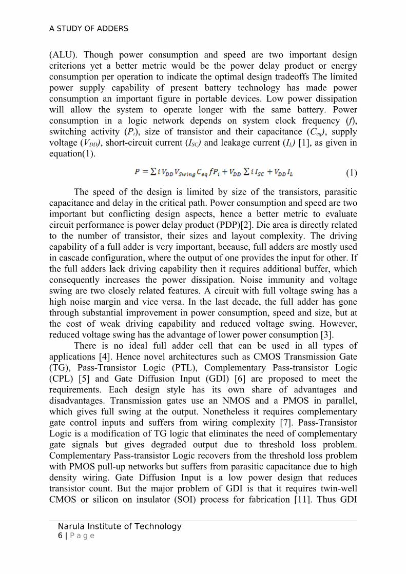
(ALU). Though power consumption and speed are two important design criterions yet a better metric would be the power delay product or energy consumption per operation to indicate the optimal design tradeoffs The limited power supply capability of present battery technology has made power consumption an important figure in portable devices. Low power dissipation will allow the system to operate longer with the same battery. Power consumption in a logic network depends on system clock frequency (f), switching activity (Pi), size of transistor and their capacitance (Ceq), supply voltage (VDD), short-circuit current (ISC) and leakage current (IL) [1], as given in equation(1).
(1)
The speed of the design is limited by size of the transistors, parasitic capacitance and delay in the critical path. Power consumption and speed are two important but conflicting design aspects, hence a better metric to evaluate circuit performance is power delay product (PDP)[2]. Die area is directly related to the number of transistor, their sizes and layout complexity. The driving capability of a full adder is very important, because, full adders are mostly used in cascade configuration, where the output of one provides the input for other. If the full adders lack driving capability then it requires additional buffer, which consequently increases the power dissipation. Noise immunity and voltage swing are two closely related features. A circuit with full voltage swing has a high noise margin and vice versa. In the last decade, the full adder has gone through substantial improvement in power consumption, speed and size, but at the cost of weak driving capability and reduced voltage swing. However, reduced voltage swing has the advantage of lower power consumption [3].
There is no ideal full adder cell that can be used in all types of applications [4]. Hence novel architectures such as CMOS Transmission Gate (TG), Pass-Transistor Logic (PTL), Complementary Pass-transistor Logic (CPL) [5] and Gate Diffusion Input (GDI) [6] are proposed to meet the requirements. Each design style has its own share of advantages and disadvantages. Transmission gates use an NMOS and a PMOS in parallel, which gives full swing at the output. Nonetheless it requires complementary gate control inputs and suffers from wiring complexity [7]. Pass-Transistor Logic is a modification of TG logic that eliminates the need of complementary gate signals but gives degraded output due to threshold loss problem. Complementary Pass-transistor Logic recovers from the threshold loss problem with PMOS pull-up networks but suffers from parasitic capacitance due to high density wiring. Gate Diffusion Input is a low power design that reduces transistor count. But the major problem of GDI is that it requires twin-well CMOS or silicon on insulator (SOI) process for fabrication [11]. Thus GDI
Narula Institute of Technology6 | P a g e
A STUDY OF ADDERS
chips are more expensive. These logic styles and their combinations (Hybrid) are commonly used in designing full adder cells.
In this paper, we have given a brief description of the evolution of full adder circuits in terms of lesser power consumption, higher speed and lesser chip size. We have started with the most conventional 28 transistor full adder and then gradually studied full adders consisting of as less as 8 transistors. We have also included some of the most popular full adder cells like Static Energy Recovery Full Adder (SERF) [7] [8], Adder9A, Adder9B, GDI based full adder.
The rest of this paper is organized as follows: First we have derived the primary expressions for the sum and carry bits for the adder. Then a brief review of the conventional adders is discussed. In the next section we have introduced some recognized 10 transistors full adder structures. Then we proceed to the proposed 8 transistor full adder circuit. Finally we conclude the paper in the next section.
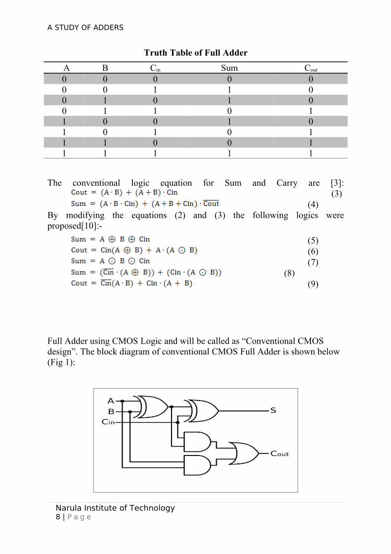
Truth Table and Equation:
A plethora of adder configurations has been reported previously. There is no ideal full adder cell that can be used in all types of applications [4]. Hence novel architectures such as CMOS, Transmission Gate (TG), Pass-Transistor Logic (PTL), Complementary Pass-transistor Logic (CPL) [5] and Gate Diffusion Input (GDI) [6] are proposed to meet the requirements. Each design style has its own share of advantages and disadvantages.
A full adder performs the addition of two bits A and B with the Carry (Cin) bit generated in the previous stage. The integer equivalent of this relation is shown by:
The conventional logic equation for Sum and Carry are [3]:(3)
(4)By modifying the equations (2) and (3) the following logics were proposed[10]:-
(5)(6)(7)
(8)(9)
Full Adder using CMOS Logic and will be called as “Conventional CMOS design”. The block diagram of conventional CMOS Full Adder is shown below (Fig 1):
Narula Institute of Technology8 | P a g e
A STUDY OF ADDERS
Figure 1: Block Diagram of Basic Full Adder
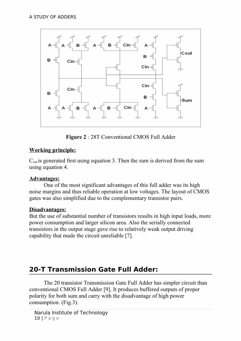
Conventional 28 T CMOS Full Adder:
On the basis of this above block diagram a complementary CMOS full adder circuit [7] was designed using 28 transistors. This adder was based on regular CMOS structure (pull-up and pull-down network) (Fig 2).
Narula Institute of Technology9 | P a g e
A STUDY OF ADDERS
Figure 2 : 28T Conventional CMOS Full Adder
Working principle:
Cout is generated first using equation 3. Then the sum is derived from the sum using equation 4.
Advantages:One of the most significant advantages of this full adder was its high
noise margins and thus reliable operation at low voltages. The layout of CMOS gates was also simplified due to the complementary transistor pairs.
Disadvantages:But the use of substantial number of transistors results in high input loads, more power consumption and larger silicon area. Also the serially connected transistors in the output stage gave rise to relatively weak output driving capability that made the circuit unreliable [7].
20-T Transmission Gate Full Adder:
The 20 transistor Transmission Gate Full Adder has simpler circuit than conventional CMOS Full Adder [9]. It produces buffered outputs of proper polarity for both sum and carry with the disadvantage of high power consumption. (Fig.3).
Narula Institute of Technology10 | P a g e
A STUDY OF ADDERS
Figure 3 : 20T Transmission Gate Full Adder
Working principle:
In the circuit we have 2 inverters followed by two transmission gates which act as 8-T XOR. Subsequently 8-T XNOR module follows. To generate sum; cin and are multiplexed which can controlled either by (a ⊕ b) or (a ⊗ b). Similarly the cout can be calculated by multiplexing a and cin which is controlled by (a ⊕ b).
Advantage:
It is the fastest adder so far been reported. The circuit is simpler than the conventional adder.
Disadvantage:
The power dissipation in this circuit is more than the 28T adder. However with same power consumption it performs faster[8].
Narula Institute of Technology11 | P a g e
A STUDY OF ADDERS
14 Transistor Full Adder:
The 14T full adder contains a 4T PTL XOR gate, shown in Fig. 4, an inverter and two transmission gates based multiplexer designs for sum and cout
signals[11].
Figure 4 : 14T Full AdderWorking principle:
This circuit has 4 transistor XOR which in the next stage is inverted to produce XNOR. These XOR and XNOR are used simultaneously to generate sum and cout. The signals cin and are multiplexed which can controlled either by (a ⊕ b) or (a ⊗ b). Similarly the cout can be calculated by multiplexing a and cin controlled by (a ⊕ b).
Advantage:
It is the fastest adder so far been reported. The circuit is simpler than the conventional adder.
Disadvantage:
The power dissipation in this circuit is more than the 28T adder. However with same power consumption it performs faster[4].
Narula Institute of Technology12 | P a g e
A STUDY OF ADDERS
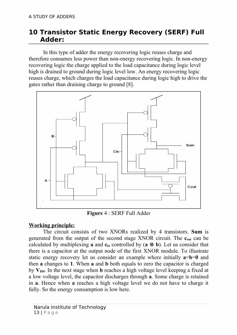
10 Transistor Static Energy Recovery (SERF) Full Adder:
In this type of adder the energy recovering logic reuses charge and therefore consumes less power than non-energy recovering logic. In non-energy recovering logic the charge applied to the load capacitance during logic level high is drained to ground during logic level low. An energy recovering logic reuses charge, which charges the load capacitance during logic high to drive the gates rather than draining charge to ground [8].
Figure 4 : SERF Full Adder
Working principle:The circuit consists of two XNORs realized by 4 transistors. Sum is
generated from the output of the second stage XNOR circuit. The cout can be calculated by multiplexing a and cin controlled by (a ⊗ b). Let us consider that there is a capacitor at the output node of the first XNOR module. To illustrate static energy recovery let us consider an example where initially a=b=0 and then a changes to 1. When a and b both equals to zero the capacitor is charged by VDD. In the next stage when b reaches a high voltage level keeping a fixed at a low voltage level, the capacitor discharges through a. Some charge is retained in a. Hence when a reaches a high voltage level we do not have to charge it fully. So the energy consumption is low here.
Narula Institute of Technology13 | P a g e
A STUDY OF ADDERS
Advantage:It is the adder so reported to be the circuit consuming power in 10t
topologies. It should be noted that the new SERF adder has no direct path to the ground. The elimination of a path to the ground reduces power consumption, removing the Psc variable (product of Isc and voltage) from the total power equation. The charge stored at the load capacitance is reapplied to the control gates. The combination of not having a direct path to ground and the re-application of the load charge to the control gate makes the energy-recovering full adder an energy efficient design. To the best of our knowledge this new design has the lowest transistor count for the complete realization.[12]
Disadvantage:The circuit produces full-swing at the output nodes. But it fails to provide
so for the internal nodes. As the power consumption by the circuit reduces the circuit becomes slower. Also it cannot be cascaded at low power supply due to multiple threshold problem [12].
Narula Institute of Technology14 | P a g e
A STUDY OF ADDERS
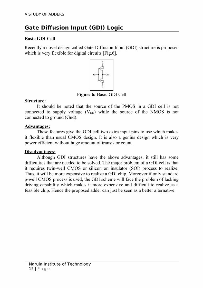
Gate Diffusion Input (GDI) Logic
Basic GDI Cell
Recently a novel design called Gate-Diffusion Input (GDI) structure is proposed which is very flexible for digital circuits [Fig.6].
Figure 6: Basic GDI CellStructure:
It should be noted that the source of the PMOS in a GDI cell is not connected to supply voltage (VDD) while the source of the NMOS is not connected to ground (Gnd).
Advantages:These features give the GDI cell two extra input pins to use which makes
it flexible than usual CMOS design. It is also a genius design which is very power efficient without huge amount of transistor count.
Disadvantages:Although GDI structures have the above advantages, it still has some
difficulties that are needed to be solved. The major problem of a GDI cell is that it requires twin-well CMOS or silicon on insulator (SOI) process to realize. Thus, it will be more expensive to realize a GDI chip. Moreover if only standard p-well CMOS process is used, the GDI scheme will face the problem of lacking driving capability which makes it more expensive and difficult to realize as a feasible chip. Hence the proposed adder can just be seen as a better alternative.
Narula Institute of Technology15 | P a g e
A STUDY OF ADDERS
GDI XOR/XNOR Gates
According to this above mentioned structure one GDI XOR and one GDI XNOR gates were proposed [Fig. 7] where only 4 transistors are used. These are as follows:
Now using these GDI based XOR and XNOR gates two different GDI based full adder architecture were designed [Fig. 8]. It should be noted that all of the proposed full adders are 10-T based. Hence, the attempt to create 10-T based full adders was achieved [14].
Circuit Operation:The circuit operation of GDI Based Full Adders are exactly the same as
that of previous SERF module. Sum bit is obtained from the output of the second stage of XOR [Fig. 8(a)] or XNOR [Fig. 8(b)] circuit while Carry bit (Cout) is calculated by multiplexing B and Cin controlled by (A XNOR B).
Advantage:These features give the GDI cell two extra input pins to use which makes
it flexible than usual CMOS design. It is also a genius design which is very power efficient without huge amount of transistor count.
Disadvantage:Although GDI structures have the above advantages, it still has some
difficulties that are needed to be solved. The major problem of a GDI cell is that it requires twin-well CMOS or silicon on insulator (SOI) process to realize. Thus, it will be more expensive to realize a GDI chip. Moreover if only standard p-well CMOS process is used, the GDI scheme will face the problem of lacking driving capability which makes it more expensive and difficult to realize as a feasible chip. Hence the proposed adder can just be seen as a better alternative.
Narula Institute of Technology17 | P a g e
A STUDY OF ADDERS
ADDER 9A and ADDER 9B:
XNOR Module:Before we present the new adders, we propose a new XNOR gate which
is named Groundless XNOR, or G-XNOR [Fig. 9] [13], because of the absence of ground node. The structure is as follows:
Figure 9: Groundless XNOR (G-XNOR)
Structure:Now based on this XNOR module two new 10-T adders are designed
[Fig.10 ] which are given below:
Figure 10(a): ADDER 9A Figure 10(b): ADDER 9B
From the above figures we can see that a Static Energy Recovery XNOR gate is cascaded with the new G-XNOR gate to generate the Sum while the Cout function is implemented by simply multiplexing B and Cin controlled by (A XNOR B) as done in the previous circuits.
Narula Institute of Technology18 | P a g e
A STUDY OF ADDERS
Advantage:
These two new adders consistently consume less power in high frequencies and have higher speed compared with the previous 10-transistor full adders and the conventional 28-transistor CMOS adder [13].
High Speed 8T Full Adder using Novel 3T XOR:
XOR Structure:
Narula Institute of Technology19 | P a g e
A STUDY OF ADDERS
3T-XOR module is the basic building block of the 8T full adder. In this section, we present the design and operation of XOR gate.
Figure 11: (a) A partial XOR and (b) Novel 3T XOR
Circuit Operation:Two PMOS transistors configured as shown in Fig.11a, are capable of
working as a XOR gate except for the input combination A=B=1. For this input combination both transistors remain off, hence the output is in high impedance state. The proposed 3T-XOR solves the problem by using a high resistance between output and ground, as given in Fig.11b. Due to technology limitations, this high resistance is realized by an NMOS with proper w/l ratio. The following illustration describes the operation of 3T-XOR.
Figure 12: Circuit operation of 3T XORFor A=B=0, both the PMOS are on. Hence the capacitor is discharged to |VTP|. The remaining charge of the capacitor is drained by M3, as shown in Fig. 12(a). For A=0 & B=1, M1 is on. The capacitor is charged to VDD. However, since M3
is on, there is some degradation in the output voltage [Fig. 12(b)]. The circuit operation is identical for A=1 & B=0. For A=B=1, both M1 & M2 are off. The capacitor is discharged by the M3 [Fig. 12(c).].
Design of 8T FULL ADDER:
Narula Institute of Technology20 | P a g e
A STUDY OF ADDERS
The basic of 8T full adder consists of 3 modules: 2 XOR elements and a Carry section as shown in figure below:
Figure 13: Transistor level implementation of 8T-Full Adder
The Sum output is obtained by two XOR blocks in succession. For the carry section we use GDI based 2T-MUX and A⊕B as the selection signal. The Sum and the Cout module need 6 and 2 transistors respectively. The transistor level implementation of the eight transistor full adder is shown in Fig. 13. It is obvious from the figure that both Sum and Cout has a maximum delay of 2T.
Advantage:It is to be noted that the new 3T-XOR has a distinct advantage over
previous 4T-XOR as it doesn’t suffer from threshold voltage loss problem. Also the noise margin has been substantially increased by proper sizing of transistors in 3T XOR. The power delay product (PDP), and the area of the proposed adder are also found better than that of the existing 10T and 14T adders.
Disadvantage:Higher power consumption due to short circuit current.
Narula Institute of Technology21 | P a g e
A STUDY OF ADDERS
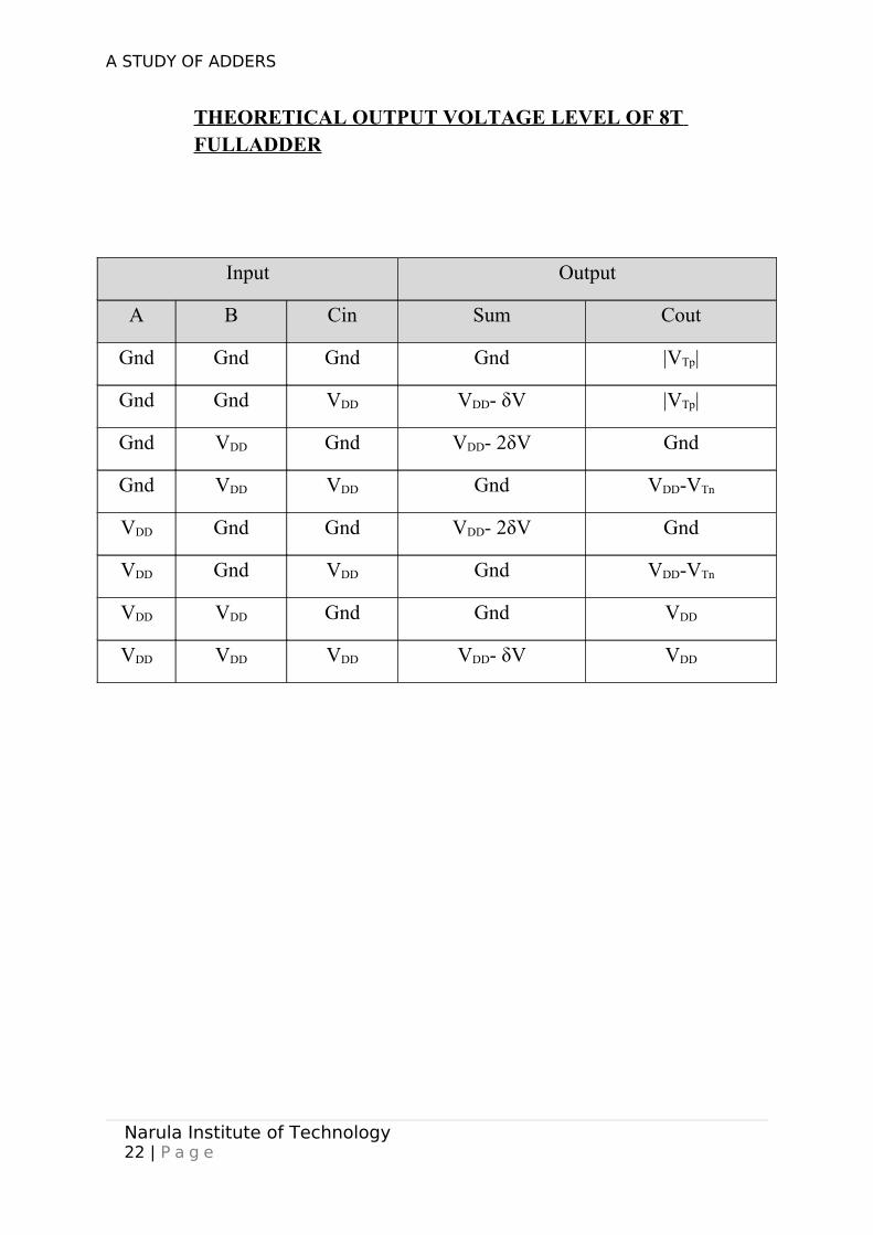
THEORETICAL OUTPUT VOLTAGE LEVEL OF 8T FULLADDER
Input Output
A B Cin Sum Cout
Gnd Gnd Gnd Gnd |VTp|
Gnd Gnd VDD VDD- δV |VTp|
Gnd VDD Gnd VDD- 2δV Gnd
Gnd VDD VDD Gnd VDD-VTn
VDD Gnd Gnd VDD- 2δV Gnd
VDD Gnd VDD Gnd VDD-VTn
VDD VDD Gnd Gnd VDD
VDD VDD VDD VDD- δV VDD
Narula Institute of Technology22 | P a g e
A STUDY OF ADDERS
OUTPUT WAVEFORM:
Narula Institute of Technology23 | P a g e
A STUDY OF ADDERS
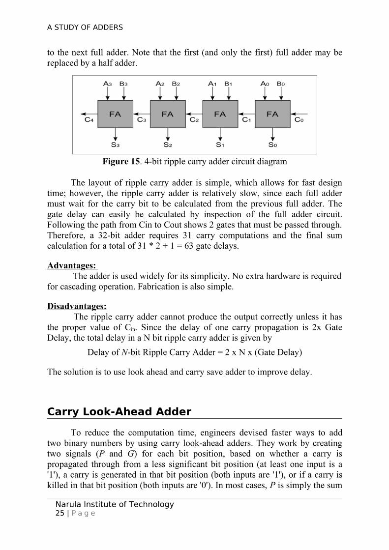
Ripple Carry Adder
It is possible to create a logical circuit using multiple full adders to add N-bit numbers. Each full adder inputs a Cin, which is the Cout of the previous adder. This kind of adder is a ripple carry adder, since each carry bit "ripples"
Narula Institute of Technology24 | P a g e
A STUDY OF ADDERS
to the next full adder. Note that the first (and only the first) full adder may be replaced by a half adder.
The layout of ripple carry adder is simple, which allows for fast design time; however, the ripple carry adder is relatively slow, since each full adder must wait for the carry bit to be calculated from the previous full adder. The gate delay can easily be calculated by inspection of the full adder circuit. Following the path from Cin to Cout shows 2 gates that must be passed through. Therefore, a 32-bit adder requires 31 carry computations and the final sum calculation for a total of 31 * 2 + 1 = 63 gate delays.
Advantages: The adder is used widely for its simplicity. No extra hardware is required
for cascading operation. Fabrication is also simple.
Disadvantages: The ripple carry adder cannot produce the output correctly unless it has
the proper value of Cin. Since the delay of one carry propagation is 2x Gate Delay, the total delay in a N bit ripple carry adder is given by
Delay of N-bit Ripple Carry Adder = 2 x N x (Gate Delay)
The solution is to use look ahead and carry save adder to improve delay.
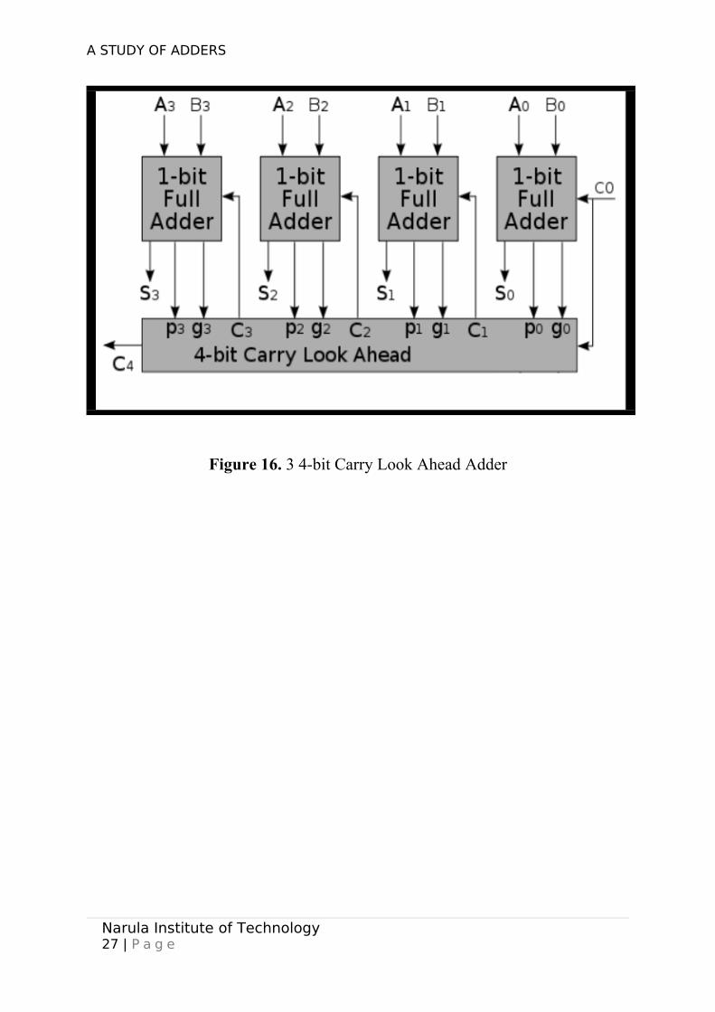
Carry Look-Ahead Adder
To reduce the computation time, engineers devised faster ways to add two binary numbers by using carry look-ahead adders. They work by creating two signals (P and G) for each bit position, based on whether a carry is propagated through from a less significant bit position (at least one input is a '1'), a carry is generated in that bit position (both inputs are '1'), or if a carry is killed in that bit position (both inputs are '0'). In most cases, P is simply the sum
General CLA Equations:Ci = Gi + Pi Ci-1 where,G= A.BSi = Pi⊕Ci-1 P= A⊕B
4Stage CLA Equations:C0 = G0 + P0Cin
C1 = G1 + P1G0 + P1P0Cin
C2 = G2 + P2G1 + P2P1G0 + P2P1P0Cin
C3 = G3 + P3G2 + P3P1G1 + P3P2P1G0 + P3P2P1P0Cin
Narula Institute of Technology26 | P a g e
A STUDY OF ADDERS
Figure 16. 3 4-bit Carry Look Ahead Adder
Narula Institute of Technology27 | P a g e
A STUDY OF ADDERS
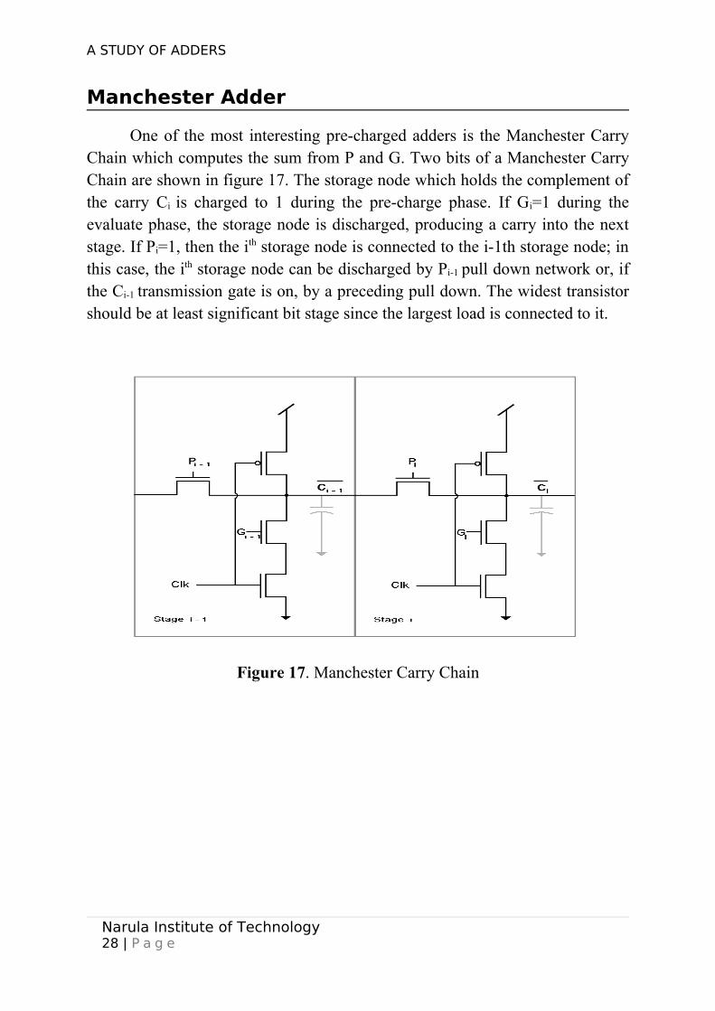
Manchester Adder
One of the most interesting pre-charged adders is the Manchester Carry Chain which computes the sum from P and G. Two bits of a Manchester Carry Chain are shown in figure 17. The storage node which holds the complement of the carry Ci is charged to 1 during the pre-charge phase. If Gi=1 during the evaluate phase, the storage node is discharged, producing a carry into the next stage. If Pi=1, then the ith storage node is connected to the i-1th storage node; in this case, the ith storage node can be discharged by Pi-1 pull down network or, if the Ci-1 transmission gate is on, by a preceding pull down. The widest transistor should be at least significant bit stage since the largest load is connected to it.
Figure 17. Manchester Carry Chain
Narula Institute of Technology28 | P a g e
A STUDY OF ADDERS
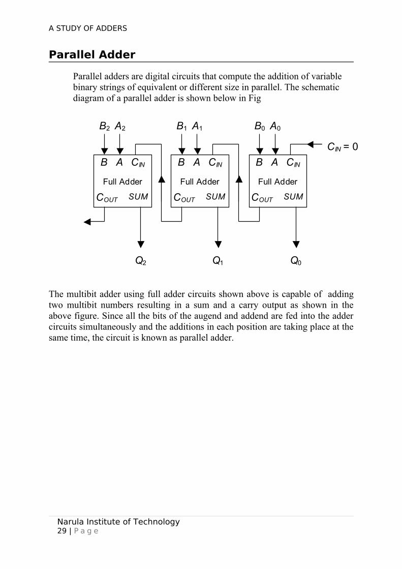
Parallel Adder
Parallel adders are digital circuits that compute the addition of variable binary strings of equivalent or different size in parallel. The schematic diagram of a parallel adder is shown below in Fig
The multibit adder using full adder circuits shown above is capable of adding two multibit numbers resulting in a sum and a carry output as shown in the above figure. Since all the bits of the augend and addend are fed into the adder circuits simultaneously and the additions in each position are taking place at the same time, the circuit is known as parallel adder.
Narula Institute of Technology29 | P a g e
Full Adder
B A CIN
COUT SUM
Full Adder
B A CIN
COUT SUM
Full Adder
B A CIN
COUT SUM
B1 A1 B0 A0 B2 A2
CIN = 0
Q1 Q0 Q2
A STUDY OF ADDERS
Designing a 4 bit Parallel Adder using 8T FA and 28T FA
Here we have designed a 4 bit parallel adder with 8T full adder and 28t full adder using TSPICE and have made a comparative study of their average power, average delay and power delay product(PDP).
***************************SPICE Netlist**************.SUBCKT INVERTER IN OUTM1 OUT IN Gnd GND NH L='l' W='wn' AD='5*wn*l' PD='2*(wn+5*l)' AS='5*wn*l' PS='2*(wn+5*l)'M2 OUT IN VDD Vdd PH L='l' W='wp' AD='5*wp*l' PD='2*(wp+5*l)' AS='5*wp*l' PS='2*(wp+5*l)'.ENDS
.subckt buffer in outX1 in o1 inverterX2 o1 out inverter.ends
.SUBCKT XOR A B outNarula Institute of Technology30 | P a g e
A STUDY OF ADDERS
M1 out B A Vdd PH L='l' W='wp' AD='5*wp*l' PD='2*(wp+5*l)' AS='5*wp*l' PS='2*(wp+5*l)'M2 out A B Vdd PH L='l' W='wp' AD='5*wp*l' PD='2*(wp+5*l)' AS='5*wp*l' PS='2*(wp+5*l)'M3 out vdd gnd gnd NH L='10*l' W='wn' AD='5*wn*l' PD='2*(wn+5*l)' AS='5*wn*l' PS='2*(wn+5*l)'.ends
.subckt adder a b cin sum coutX1 a b o1 XORX2 o1 cin sum XORM2 A o1 cout vdd PH L='l' W='wp' AD='5*wp*l' PD='2*(wp+5*l)' AS='5*wp*l' PS='2*(wp+5*l)'M3 Cin o1 cout gnd NH L='l' W='wn' AD='5*wn*l' PD='2*(wn+5*l)' AS='5*wn*l' PS='2*(wn+5*l)'.ends
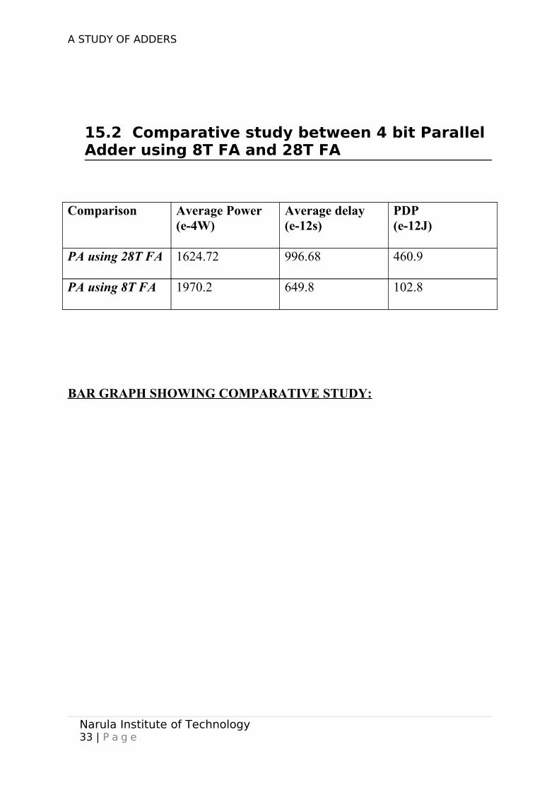
15.2 Comparative study between 4 bit Parallel Adder using 8T FA and 28T FA
Comparison Average Power(e-4W)
Average delay (e-12s)
PDP(e-12J)
PA using 28T FA 1624.72 996.68 460.9
PA using 8T FA 1970.2 649.8 102.8
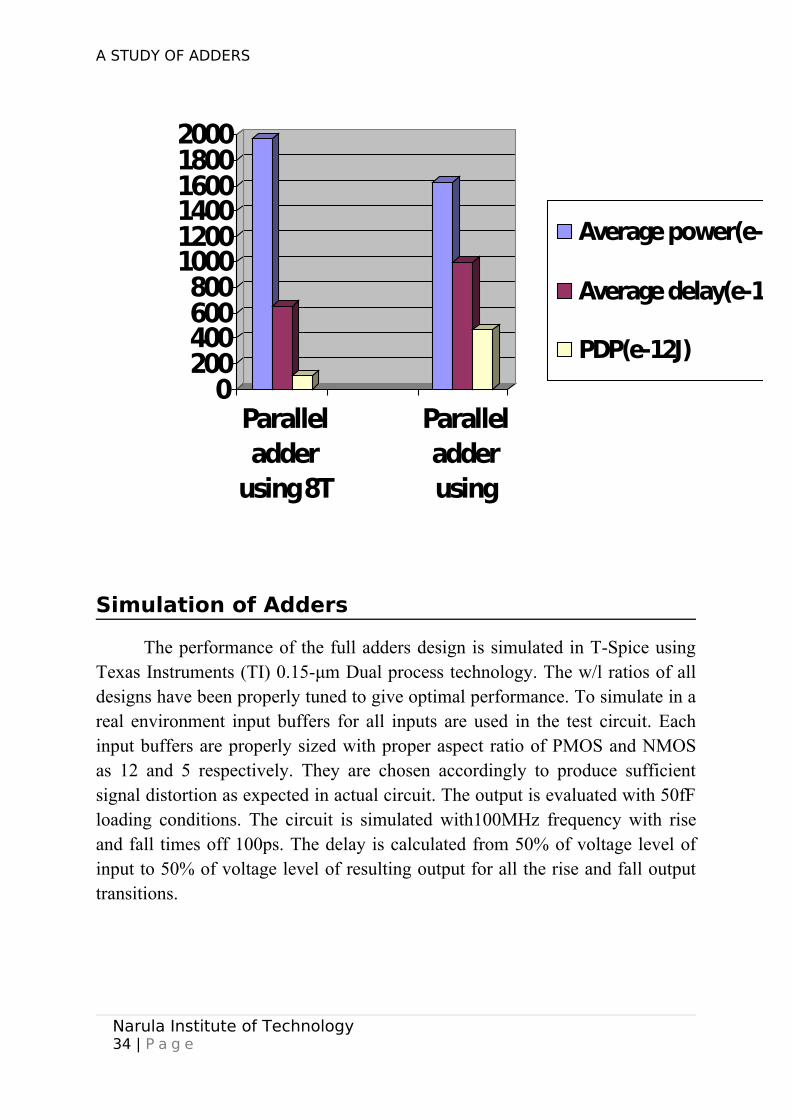
BAR GRAPH SHOWING COMPARATIVE STUDY:
Narula Institute of Technology33 | P a g e
A STUDY OF ADDERS
0200400600800
100012001400160018002000
Paralleladder
using 8TFA
Paralleladderusing28T FA
Average power(e-4W)
Average delay(e-12s)
PDP(e-12J)
Simulation of Adders
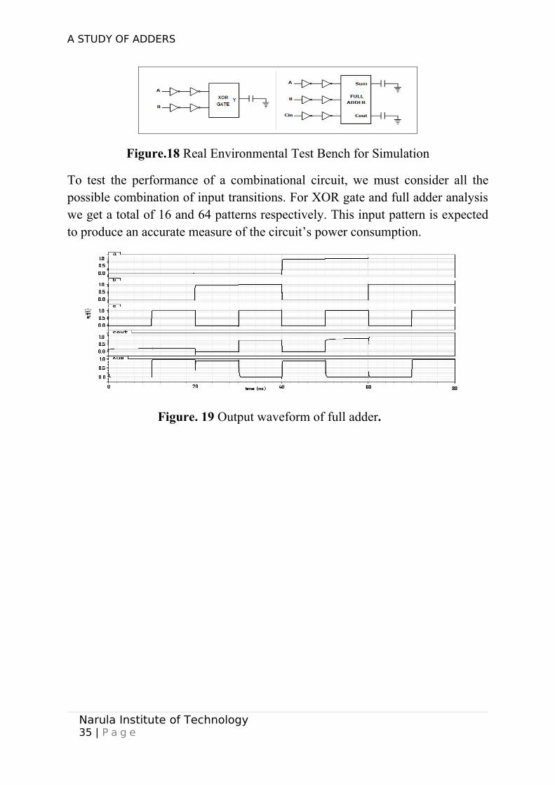
The performance of the full adders design is simulated in T-Spice using Texas Instruments (TI) 0.15-μm Dual process technology. The w/l ratios of all designs have been properly tuned to give optimal performance. To simulate in a real environment input buffers for all inputs are used in the test circuit. Each input buffers are properly sized with proper aspect ratio of PMOS and NMOS as 12 and 5 respectively. They are chosen accordingly to produce sufficient signal distortion as expected in actual circuit. The output is evaluated with 50fF loading conditions. The circuit is simulated with100MHz frequency with rise and fall times off 100ps. The delay is calculated from 50% of voltage level of input to 50% of voltage level of resulting output for all the rise and fall output transitions.
Narula Institute of Technology34 | P a g e
A STUDY OF ADDERS
Figure.18 Real Environmental Test Bench for Simulation
To test the performance of a combinational circuit, we must consider all the possible combination of input transitions. For XOR gate and full adder analysis we get a total of 16 and 64 patterns respectively. This input pattern is expected to produce an accurate measure of the circuit’s power consumption.
Figure. 19 Output waveform of full adder.
Narula Institute of Technology35 | P a g e
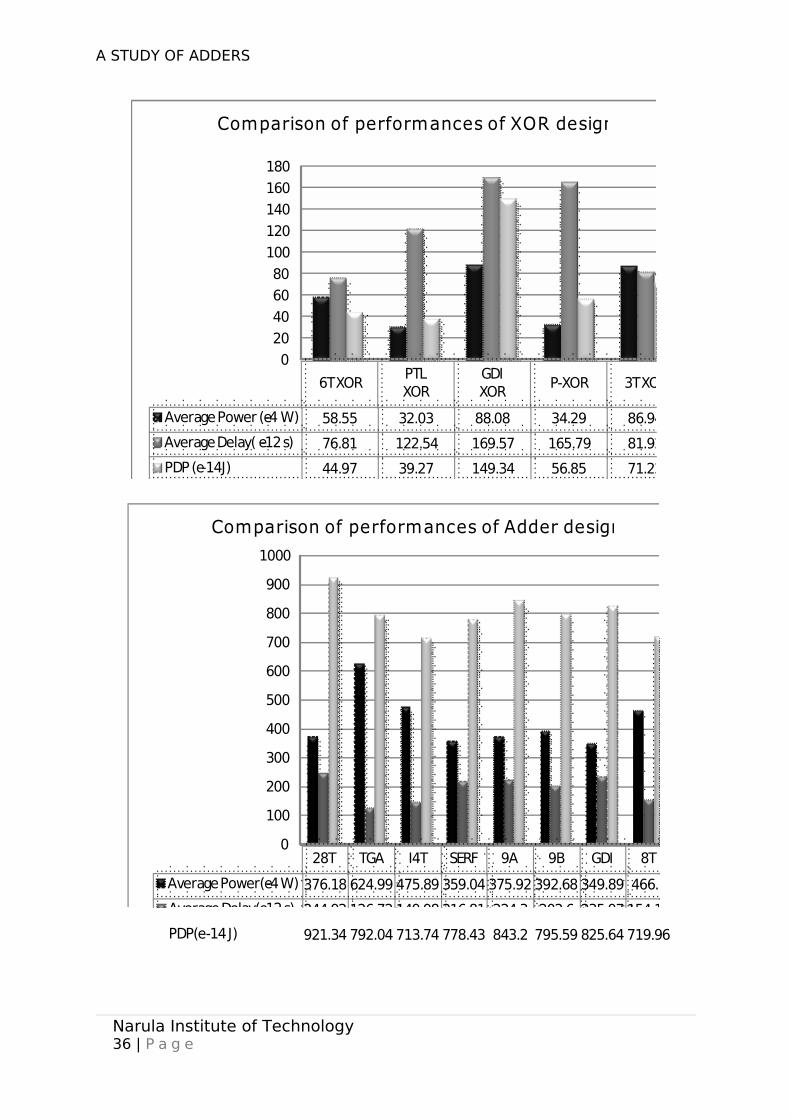
A STUDY OF ADDERS
6T XORPTL XOR
GDI XOR
P-XOR 3T XOR
Average Power (e-4 W) 58.55 32.03 88.08 34.29 86.94
Average Delay( e-12 s) 76.81 122.54 169.57 165.79 81.92
Highlights: 28T and SERF are best in power consumption.
TGA is the Fastest Adder.
14T and 8T are best in PDP.
Smallest Adder is 8T.
Narula Institute of Technology37 | P a g e
A STUDY OF ADDERS
Conclusion and Future Works
Full Adders is the heart of any digital processor. Here we have shown the implementation of I bit adders using MOSFET. However recent researches have shown that Carbon-Nano-Tubes have a huge potential in logic circuits. Not only will it reduce power consumption, but also increase speed substantially.
Narula Institute of Technology38 | P a g e
A STUDY OF ADDERS
REFERENCE
[1] A. Chandrakasan, R. Brodersen, “Low Power Design”, Kluwer Academic Publishers, 1995.
[2] A. M. Shams, and M. A. Bayoumi, “A Novel High Performance CMOS 1-Bit Full Adder Cell”, IEEE Transactions on Circuit and System, vol.47, NO. 5, May, 2000.
[3] J. H. Kang and J. B. Kim, “Design of a Low Power CVSL Full Adder Using Low-Swing Technique”, ICSE2004 Proc. 2004, Kuala Lumpur, Malaysia.
[4] A. A. Khatibzadeh and K. Raahemifar, “A Study and Comparison of Full Adder Cells based on the Standard Static CMOS Logic.”, IEEE CCECE 2004 - CCGEI 2004, Niagara Falls, May 2004.
[5] S. M. Kang and Y. Leblebici, “CMOS Digital Integrated Circuits: Analysis and Design”, Third Edition, Tata McGraw-Hill Edition 2003, pp 307-316.
[6] A. Morgenshtein, A. Fish and A. Wagner, “Gate-Diffusion Input(GDI): A Power-Efficient Method for Digital Combinational Circuits”, IEEE Trans. VLSI Syst., pp. 566-581, Oct. 2002.
[7] I. Hassoune, D.Flandre, I. O’Connor and J. D. Legat, “ULPFA: a new efficient design of a power aware full adder”, IEEE Transactions on Circuits and Systems I-5438, 2008.
[8] R. Zimmermann and W. Fichter, “Low –power logic styles: CMOS versus pass-transistor logic,” IEEE J. Solid-State Circuits, Vol. 32, July 1997, pp.1079-90
[9] N. Weste and K. Eshraghian, “Principles of VLSI Design, A System Perspective”, Reading, MA: Addison-Wesley, 1993.
[10] N. Zhuang and H. Wu, “New Design of the CMOS Full Adder”, IEEE J. Solid-State Circuits, vol. 27,no. 5,pp. 840-844, May 1992
[11] J. Wang, S. Fang, and W. Feng, “New efficient designs for XOR and XNOR functions on the transistor level”, IEEE J. Solid-State Circuits, vol. 29, no. 7, Jul. 1994, pp. 780–786.
[12] R. Shalem, E. John, and L. K. John, “A Novel Low Power Energy Recovery Full Adder Cell” in Proc. IEEE Great Lakes VLSI Symp., pp. 380–383, Feb. 1999.
[13] H. T. Bui, A. K. Al-Sheraidah and Y. Wang, “Design and Analysis of 10-transistor Full Adders using Novel XOR-XNOR Gates” , Proceedings of ICSP2000.
[14] P. M. Lee, C. H. Hsu, and Y. H. Hung, “Novel 10-T full adders realized by GDI structure” IEEE International Symposium on Integrated Circuits (ISIC-2007).
[15] J. F. Lin, Y. T. Hwang, M. H. Sheu and C. C. Ho, “A novel High-Speed and Energy Efficient 10-Transistor Full Adder Design”, IEEE
Narula Institute of Technology39 | P a g e
A STUDY OF ADDERS
Transactions on Circuits and System—I: Regular Papers, VOL. 54, NO. 5, May 2007.
[16] D. Radhakrishnan, “Low-voltage low-power CMOS full adder,” in Proc. IEEE Circuits Devices Systems, vol. 148, FEB 2001, pp 19-24.
[17] S. Goel, A. Kumar, M. A. Bayoumi, “Design of Robust, Energy-Efficient Full Adders for Deep-Submicrometer Design Using Hybrid-CMOS Logic”, IEEE Transactions on VLSI 2006