205
Transistors 6240-15-1E ITT INTERMETALL
| Date post: | 20-Apr-2018 |
| Category: |
Documents |
| Upload: | hoangduong |
| View: | 231 times |
| Download: | 9 times |

Transistors
6240-15-1E ITT INTERMETALL
2 ITT INTERMETALL
All information and data contained in this data book are with-out any commitment, are not to be considered as an offerfor conclusion of a contract nor shall they be construed asto create any liability. Any new issue of this data book, orindividual product data sheets, invalidate previous issues.Product availability and delivery dates are exclusively sub-ject to our respective order confirmation form; the sameapplies to orders based on development samples delivered.By this publication, INTERMETALL does not assume respon-sibility for patent infringements or other rights of third partieswhich may result from its use.Reprinting is generally permitted, indicating the source.However, our prior consent must be obtained in all cases.
Printed in GermanyImprimé dans la République Fédérale d’Allemagne byRombach GmbH Druck- und Verlagshaus, 79115 Freiburg
Edition September 1996 • Order No. 6240-15-1E
ITT INTERMETALL 3
Page Contents
195 to 199 Bias Resistor Transistors
201 to 204 Addresses
Alphanumerical List of Types
4 List of Types
189 to 193 Darlington Transistors
5 to 17 Technical Information
19 to 65 Small-Signal Transistors (NPN)
67 to 113 Small-Signal Transistors (PNP)
115 to 157 DMOS Transistors (N-Channel)
159 to 187 DMOS Transistors (P-Channel)
4 ITT INTERMETALL
Type Page
Small-Signal Transistors(NPN)
2N3904 202N4124 24BC337-16, -25, -40 30BC338-16, -25, -40 30BC546-A, -B 36BC547-A, -B, -C 36BC548-A, -B, -C 36BC549-B, -C 36BC817-16, -25, -40 42BC818-16, -25, -40 42BC846-A, -B 48BC847-A, -B, -C 48BC848-A, -B, -C 48BC849-B, -C 48BF420 54BF422 54BF820 56BF822 56MMBT3904 58MMBTA42 62MMBTA43 62MPSA42 64MPSA43 64
DMOS Transistors(N-Channel)
2N7000 1162N7002 122BS108 128BS109 134BS123 136BS170 138BS623 136BS809 144BS828 146BS870 152
Darlington Transistors
BCV27 190BCV26 192
Type Page
Small-Signal Transistors(PNP)
2N3906 682N4126 72BC327-16, -25, -40 78BC328-16, -25, -40 78BC556-A, -B 84BC557-A, -B, -C 84BC558-A, -B, -C 84BC559-A, -B, -C 84BC807-16, -25, -40 90BC808-16, -25, -40 90BC856-A, -B 96BC857-A, -B, -C 96BC858-A, -B, -C 96BC859-A, -B, -C 96BF421 102BF423 102BF821 104BF823 104MMBT3906 106MMBTA92 110MMBTA93 110MPSA92 112MPSA93 112
DMOS Transistors(P-Channel)
BS208 160BS209 166BS223 168BS250 170BS723 176BS808 178BS829 180BS850 182
Bias Resistor Transistors
DTC114EK 196DTC124XK 198
List of Types

ITT INTERMETALL 5
Technical Information
6 ITT INTERMETALL
Technical Information
Index of Symbols
b Imaginary part of y-Parametersbf Imaginary part of forward
transconductance yfbi Imaginary part of input admittance yibo Imaginary part of output admittance yobr Imaginary part of reverse
transconductance yrB Base connectionBG Imaginary part of generator (source)
impedanceC Capacitance; junction capacitance;
collector connectionCi Input capacitance (bi/2 π f)Co Output capacitance (bo/2 π f)CCBO Collector-Base capacitance (open emitter)CEBO Emitter-base capacitance (open collector)Ciss Input capacitanceCr Feedback capacitance (br/2 π f)E Emitter connectionf FrequencyfT Gain-bandwidth productF Noise figureFc Noise figure in mixer stagesg Real part of y-parametersgf Real part of forward transconductance yfgi Real part of input admittance yigm Forward transconductancego Real part of output admittance yogr Real part of reverse transconductance yrgs Generator conductanceGC Current gainGP Power gainGP av Available power gainGP max Max. available power gainGV Voltage gainh Parameters of h- (hybrid) matrixhf Small-signal current gainhi Input impedanceho Output admittancehr Reverse voltage transfer ratiohFE DC current gain, common emitterIB Base currentIBM Peak base currentIB1 Turn-on currentIB2 Turn-off currentIC Collector currentICAV Average collector currentICBO Collector-base cutoff current (open emitter)ICEO Collector-emitter cutoff current (open base)ICER Collector-emitter cutoff current (specified
resistance between base and emitter)
ICES Collector-emitter cutoff current (base short-circuited to emitter)
ICEV Collector-emitter cutoff current (specified voltage between base and emitter)
ICM Peak collector currentID Drain currentIDSS Drain cutoff currentIE Emitter currentIEBO Emitter-base cutoff current (open collector)IGSS Gate-body leakage currentKV Thermal resistance correction factorPtot Power dissipationPD Continuous power dissipationPI Pulse power dissipationrb’ · CC Collector-base time constantrDS (ON) Drain-source-on resistancerthA Pulse thermal resistance junction
to ambient airrthC Pulse thermal resistance junction to caseR Resistance; resistorRBE Resistance between base and emitterRG Generator impedance; source impedanceRG opt Optimum (matched) generator resistanceRL Load resistanceRL opt Optimum (matched) load resistanceRS Series resistanceRth Thermal resistanceRthA Thermal resistance junction to ambient airRthC Thermal resistance junction to case
resp. mounting baseRthC/S Thermal resistance case or mounting base
to heat sinkRthS Thermal resistance heat sink to ambient airt Timetd Delay timetf Fall Timetoff Turn-off time (ts + tf)ton Turn-on time (td + tr)tp Pulse durationtpd Propagation delay timetr Rise timets Storage timettotal Total switching time (ton + toff)T Temperature; duration of one periodTamb Ambient temperatureTj Junction temperatureTC Case temperatureTS Storage temperatureTSB Temperature of substrate backsideV VoltageVBB Base supply voltageVBE Base-emitter voltageVBE sat Base-emitter saturation voltage
ITT INTERMETALL 7
Technical Information
V(BR)CBO Collector-base breakdown voltage(open emitter)
V(BR)CEO Collector-emitter breakdown voltage(open base)
V(BR)CER Collector-emitter breakdown voltage(specified resistance between base and emitter)
V(BR)CES Collector-emitter breakdown voltage(emitter short-circuited to base)
VDGS Drain-gate voltageVDSS Drain-source voltageV(BR)DSS Drain-source breakdown voltageV(BR)EBO Emitter-base breakdown voltage
(open collector)VCB Collector-base voltageVCBO Collector-base voltage (open emitter)VCC Collector supply voltageVCE Collector-emitter voltageVCEO Collector-emitter voltage (open base)VCER Collector-emitter voltage (specified
resistance between base and emitter)VCES Collector-emitter voltage (emitter short-
circuited to base)VCE sat Collector-emitter saturation voltageVCEV Collector-emitter voltage (specified voltage
between base and emitter)VEBO Emitter-base voltage (open collector)VEE Emitter supply voltageVGS(TO) Gate threshold voltageVi Input voltageVo Output voltagey Parameters of y- (admittance) matrixyf Forward transconductanceyi Input admittanceyo Output admittanceyr Reverse transconductanceys Generator admittanceZ1 Input impedanceZ2 Output impedanceϕ Phase angle of y-parametersτs Storage time constantν Duty cycle (tp/T)
8 ITT INTERMETALL
Technical Information
Characteristics and Maximum Ratings
The electrical performance of a semiconductor deviceis usually expressed in terms of its characteristics andmaximum ratings.
Characteristics are those which can be measured byuse of suitable measuring instruments and circuits,and provide information on the performance of thedevice under specified operating conditions (at a givenbias, for example). Depending on requirements, theyare quoted either as typical (Typ.) values or guaranteed(Min., Max.) values.
Typical values are expressed as figures or as one ormore curves, and are subject to spreads. Occasionallya typical curve is accompanied by another curve, thisbeing a 95%, or, in a few cases, a maximum spreadlimit curve.
Maximum Ratings give the values which cannot beexceeded without risk of damage to the device.Changes in supply voltage and in the tolerances ofother components in the circuit must also be taken intoconsideration. No single maximum rating should everbe exceeded, even when the device is operated wellwithin the other maximum ratings. The inclusion of theword “admissible” in a title means that the associatedcurve defines the maximum ratings.
An exception to this rule are data on collector current.The collector current, quoted as one of the criticaltransistor values, is a maximum value recommendedby the manufacturer which should be noted in connec-tion with the other characteristics valid for this collec-tor current (e.g. collector and saturation voltages,current gain etc.) when selecting a transistor. In certaincases, the quoted collector current may be exceededwithout the transistor being destroyed. The absolutelimit for the collector current is determined by themaximum admissible power dissipation of the tran-sistor.
Assembly and Soldering Instructions
To prevent transistors from being damaged duringmounting, observe the following points:
All semiconductor devices are extremely sensitive totheir maximum admissible junction temperature beingexceeded. When planning the layout of the equipment,the distance between heat sources and semiconduc-tor elements should be sufficiently large.
Semiconductor elements may be mounted in anydesired position.
From the experience gained in soldering semiconduc-tor elements the following rules have emerged:
For transistors in plastic case TO-92 the maximum sol-dering time is 8 s, at soldering temperatures between230 and 260 °C. Here, the distance between solderedjoint and case should be at least 4 mm. During solder-ing, the leads should not be subjected to mechanicalstress.
For transistors in plastic case SOT-23 the maximumsoldering time is 8 s, at maximum soldering tempera-tures between 230 and 260 °C.
Technical Information
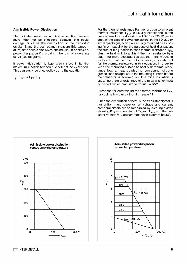
Admissible Power Dissipation
The indicated maximum admissible junction temper-ature must not be exceeded because this coulddamage or cause the destruction of the transistorcrystal. Since the user cannot measure this temper-ature, data sheets also reveal the maximum admissiblepower dissipation Ptot usually in the form of a deratingcurve (see diagram).
If power dissipation is kept within these limits themaximum junction temperature will not be exceeded.This can easily be checked by using the equation
Tj = Tamb + Ptot · Rth
ITT INTERMETALL
Admissible power dissipation versus ambient temperature
mW500
Ptot
300
200
10000
100
Tamb
200 °C
400
For the thermal resistance Rth the junction to ambientthermal resistance RthA is usually substituted in thecase of small transistors (in the TO-18 or TO-92 pack-age). In the case of power transistors (in the TO-202 orsimilar packages) which are usually mounted on a cool-ing fin or heat sink for the purpose of heat dissipation,the sum of the junction to case thermal resistance RthCplus the heat sink to ambient thermal resistance RthSplus – for more accurate calculations – the mountingsurface to heat sink thermal resistance, is substitutedfor the thermal resistance in this equation. In order tokeep the mounting surface to heat sink thermal resis-tance low, a heat conducting compound (siliconegrease) is to be applied to the mounting surface beforethe transistor is screwed on. If a mica insulation isused, the thermal resistance of the mica washer mustbe added, which amounts to about 0.5 K/W.
Directions for determining the thermal resistance RthSfor cooling fins can be found on page 11.
Since the distribution of heat in the transistor crystal isnot uniform and depends on voltage and current,some transistors are accompanied by derating curvesshowing Ptot as a function of TC and Tamb with the col-lector voltage VCE as parameter (see diagram below).
VCE
8 V
Admissible power dissipation versus temperature
W5
Ptot
3
2
10000
1
Tamb,
200 °C
4
TC
thAR = 200 K/W
40 V
20 V
10 V
= 0...7 V
RthC = 35 K/W
9
10 ITT INTERMETALL
Technical Information
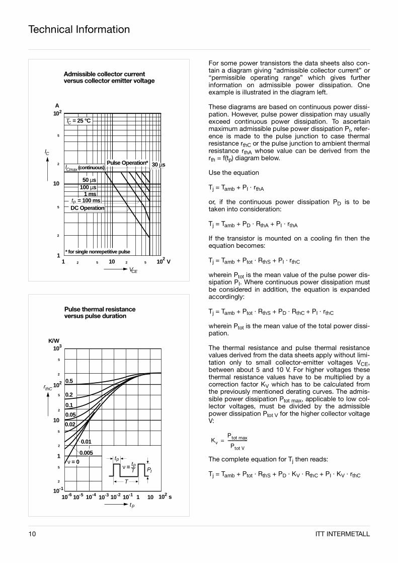
For some power transistors the data sheets also con-tain a diagram giving “admissible collector current” or“permissible operating range” which gives furtherinformation on admissible power dissipation. Oneexample is illustrated in the diagram left.
These diagrams are based on continuous power dissi-pation. However, pulse power dissipation may usuallyexceed continuous power dissipation. To ascertainmaximum admissible pulse power dissipation PI, refer-ence is made to the pulse junction to case thermalresistance rthC or the pulse junction to ambient thermalresistance rthA whose value can be derived from therth = f(tp) diagram below.
Use the equation
Tj = Tamb + PI · rthA
or, if the continuous power dissipation PD is to betaken into consideration:
Tj = Tamb + PD · RthA + PI · rthA
If the transistor is mounted on a cooling fin then theequation becomes:
Tj = Tamb + Ptot · RthS + PI · rthC
wherein Ptot is the mean value of the pulse power dis-sipation PI. Where continuous power dissipation mustbe considered in addition, the equation is expandedaccordingly:
Tj = Tamb + Ptot · RthS + PD · RthC + PI · rthC
wherein Ptot is the mean value of the total power dissi-pation.
The thermal resistance and pulse thermal resistancevalues derived from the data sheets apply without limi-tation only to small collector-emitter voltages VCE,between about 5 and 10 V. For higher voltages thesethermal resistance values have to be multiplied by acorrection factor KV which has to be calculated fromthe previously mentioned derating curves. The admis-sible power dissipation Ptot max, applicable to low col-lector voltages, must be divided by the admissiblepower dissipation Ptot V for the higher collector voltageV:
The complete equation for Tj then reads:
Tj = Tamb + Ptot · RthS + PD · KV · RthC + PI · KV · rthC
KvPtot max
Ptot V
-----------------=
Pulse thermal resistance versus pulse duration
K/W
rthC
1
tp
2
103
5
102
5
2
10
5
2
5
2
10-1
10-6 10-4 10-2 1 10 s2
0.5
0.1
0.05
0.02
0.01
tpν = tp
T PI
T
ν = 0
10-5 10-3 10-1 10
0.2
0.005
10
5
5
1011
2
V10 V
2
2
10
2 5 2 52
* for single nonrepetitive pulse
TC = 25 °C
ICmax (continuous)
50 µs100 µs
1 ms= 100 mstp
DC Operation
Admissible collector current versus collector emitter voltage
A
IC
CE
Pulse Operation* 30 µs
ITT INTERMETALL 11
Technical Information
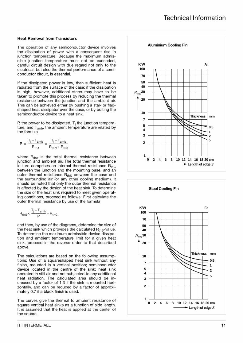
Heat Removal from Transistors
The operation of any semiconductor device involvesthe dissipation of power with a consequent rise injunction temperature. Because the maximum admis-sible junction temperature must not be exceeded,careful circuit design with due regard not only to theelectrical, but also the thermal performance of a semi-conductor circuit, is essential.
If the dissipated power is low, then sufficient heat isradiated from the surface of the case; if the dissipationis high, however, additional steps may have to betaken to promote this process by reducing the thermalresistance between the junction and the ambient air.This can be achieved either by pushing a star- or flag-shaped heat dissipator over the case, or by bolting thesemiconductor device to a heat sink.
P, the power to be dissipated, Tj the junction tempera-ture, and Tamb, the ambient temperature are related bythe formula
where RthA is the total thermal resistance betweenjunction and ambient air. The total thermal resistancein turn comprises an internal thermal resistance RthCbetween the junction and the mounting base, and anouter thermal resistance RthS between the case andthe surrounding air (or any other cooling medium). Itshould be noted that only the outer thermal resistanceis affected by the design of the heat sink. To determinethe size of the heat sink required to meet given operat-ing conditions, proceed as follows: First calculate theouter thermal resistance by use of the formula
and then, by use of the diagrams, determine the size ofthe heat sink which provides the calculated RthS-value.To determine the maximum admissible device dissipa-tion and ambient temperature limit for a given heatsink, proceed in the reverse order to that describedabove.
The calculations are based on the following assump-tions: Use of a squareshaped heat sink without anyfinish, mounted in a vertical position; semiconductordevice located in the centre of the sink; heat sinkoperated in still air and not subjected to any additionalheat radiation. The calculated area should be in-creased by a factor of 1.3 if the sink is mounted hori-zontally, and can be reduced by a factor of approxi-mately 0.7 if a black finish is used.
The curves give the thermal to ambient resistance ofsquare vertical heat sinks as a function of side length.It is assumed that the heat is applied at the center ofthe square.
PTj Tamb–
RthA
--------------------Tj Tamb–
RthC RthS+--------------------------= =
RthS
Tj Tamb–
P-------------------- RthC–<
Aluminium Cooling Fin
K/W100
RthS
7
1001
Length of edge S20 cm
Al
70
504030
20
10
54
3
2
2 4 6 8 12 14 16 18
1
52
0.5
Thickness mm
Steel Cooling Fin
K/W100
RthS
7
1001
Length of edge S20 cm
Fe
70
504030
20
10
54
3
2
2 4 6 8 12 14 16 18
1
5
2
0.5
Thickness mm
12 ITT INTERMETALL
Technical Information
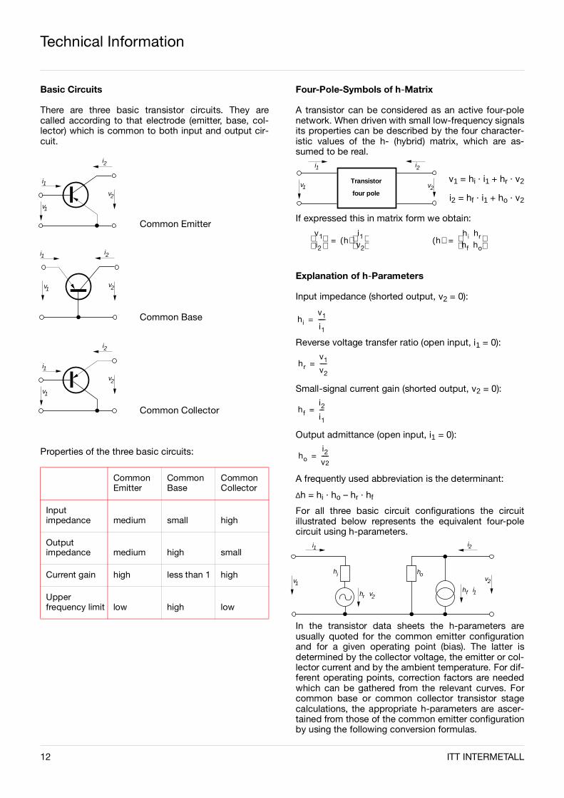
Basic Circuits
There are three basic transistor circuits. They arecalled according to that electrode (emitter, base, col-lector) which is common to both input and output cir-cuit.
Common Emitter
Common Base
Common Collector
Properties of the three basic circuits:
CommonEmitter
CommonBase
CommonCollector
Inputimpedance medium small high
Outputimpedance medium high small
Current gain high less than 1 high
Upperfrequency limit low high low
Four-Pole-Symbols of h-Matrix
A transistor can be considered as an active four-polenetwork. When driven with small low-frequency signalsits properties can be described by the four character-istic values of the h- (hybrid) matrix, which are as-sumed to be real.
v1 = hi · i1 + hr · v2
i2 = hf · i1 + ho · v2
If expressed this in matrix form we obtain:
Explanation of h-Parameters
Input impedance (shorted output, v2 = 0):
Reverse voltage transfer ratio (open input, i1 = 0):
Small-signal current gain (shorted output, v2 = 0):
Output admittance (open input, i1 = 0):
A frequently used abbreviation is the determinant:
∆h = hi · ho – hr · hf
For all three basic circuit configurations the circuitillustrated below represents the equivalent four-polecircuit using h-parameters.
In the transistor data sheets the h-parameters areusually quoted for the common emitter configurationand for a given operating point (bias). The latter isdetermined by the collector voltage, the emitter or col-lector current and by the ambient temperature. For dif-ferent operating points, correction factors are neededwhich can be gathered from the relevant curves. Forcommon base or common collector transistor stagecalculations, the appropriate h-parameters are ascer-tained from those of the common emitter configurationby using the following conversion formulas.
v1i2
h( )i1v2
""dfoisdufoifus h( )hiahrhfaho
= =
hiv1
i1----=
hrv1
v2----=
hf
i2i1---=
ho
i2v2----=
v1
i1
i2
v2
v1
i1 i2
v2
v1
i1
i2
v2
v1
i1 i2
v2Transistor
four pole
v1
i1 i2
v2
hf · i1hr · v2
hohi
13 ITT INTERMETALL
CommonEmitter
CommonBase
CommonCollector
Input impedance hie –hic = hie
Reverse voltage transfer ratio hre –hrc = 1 – hre
Small-signal current gain hfe –hfc = 1 + hfe
Output admittance hoe –hoc = hoe
hib
hie
1 hfe+---------------=
hrb
hie hoe⋅
1 hfe+------------------ hre–=
hfb
hfe
1 hfe+---------------–=
hob
hoe
1 hfe+---------------=
Technical Information
Calculation of a Transistor Stage
Input impedance
Output impedance
Current gain
Voltage gain
Power gain
Max. available power gain, input and output matchedwith RG opt resp. RL opt
Z1v1
i1----
hi RL hD⋅+
1 ho RL⋅+-------------------------= =
Z2v2
i2----
hi RG+
hD ho RG⋅+---------------------------= =
Gc
i2i1---
hf
1 ho RL⋅+-----------------------= =
Gv
v2
v1
----hf– RL⋅
hi RL hD⋅+-------------------------= =
Gpv2 i2⋅
v1 i1⋅------------
hf2 RL⋅
1 ho RL⋅+( ) hi RL hD⋅+( )---------------------------------------------------------= =
Gp max
hf
hD hi ho⋅+--------------------------------
2
=
RG opthi hD⋅
ho
--------------= RL opthi
ho hD⋅---------------=
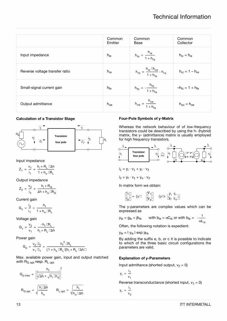
Four-Pole Symbols of y-Matrix
Whereas the network behaviour of of low-frequencytransistors could be described by using the h- (hybrid)matrix, the y- (admittance) matrix is usually employedfor high frequency transistors.
i1 = yi · v1 + yr · v2
i2 = yf · v1 + yo · v2
In matrix form we obtain:
The y-parameters are complex values which can beexpressed as
yik = gik + jbik with bik = ωCik or with bik =
Often, the following notation is expedient:
yik = l yik l exp jϕik
By adding the suffix e, b, or c it is possible to indicateto which of the three basic circuit configurations theparameters are valid.
Explanation of y-Parameters
Input admittance (shorted output, v2 = 0)
Reverse transconductance (shorted input, v1 = 0)
i1
i2
y( )=V1
V2
y( )yi yryf yo
=
1
ωLik
---------–
yi
i1v1
----=
yr
i1v2
----=
v1 v2Transistor
four poleZ1
RG
Z2RL
i1 i2
v1
i1 i2
v2Transistorfour pole
v1
i1 i2
v2
y r· v
2y f
· v1
yoyi
14 ITT INTERMETALL
Technical Information
Forward transconductance (shorted output, v2 = 0)
Output admittance (shorted input, v1 = 0)
The determinant reads Dy = yi · yo – yr · yf
Conversion from y-Parameters to h-Parameters
Calculation of a Transistor Stage
Input impedance
Output impedance
Current gain
Voltage gain
Power gain
Available power gain, input matched with RG opt
Max. available power gain, input and output matchedwith RG opt resp. RL opt
Max. available power gain will be attained if input andoutput are matched, where:
and:
Dy = yi · yo – yr · yf
yf
i2v1
----=
yoi2v2
----=
hi1yi
---= hryr
yi----–= hD
yo
yi
-----=
hfyf
yi---= ho
yD
yi------=
Z1v1
i1----
1 yo RL⋅+
yi yD RL⋅+-------------------------= =
Z2v2
i2----
1 yi RG⋅+
yo yD RG⋅+---------------------------= =
Gci2i1---
yf
yi yD RL⋅+-------------------------= =
Gvv2
v1
----yf– RL⋅
1 yo RL⋅+-----------------------= =
Gpv2 i2⋅
v1 i1⋅------------
yf2 RL⋅
1 yo RL⋅+( ) yi yD RL⋅+( )---------------------------------------------------------= =
Gp av4 yf
2 RG RL⋅ ⋅ ⋅
y1 yD RL) RG 1 yo RL⋅+ +⋅ ⋅+([ ]2--------------------------------------------------------------------------=
Gp max
yf
yD yi yo⋅+-------------------------------
2
=
RL optyo
yi
----- 1
yD------⋅=
RG optyi
yo
----- 1
yD------⋅=
v1
i1 i2
v2Transistor
four poleZ1
RGZ2 RL
ITT INTERMETALL 15
Technical Information
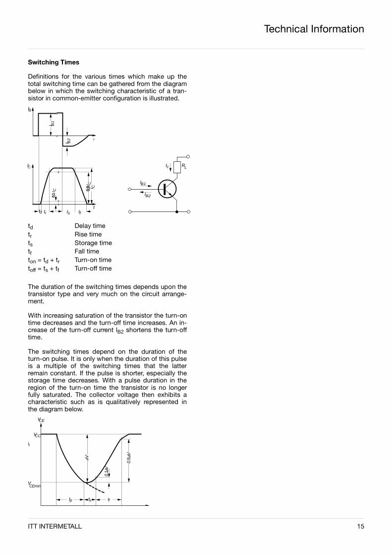
Switching Times
Definitions for the various times which make up thetotal switching time can be gathered from the diagrambelow in which the switching characteristic of a tran-sistor in common-emitter configuration is illustrated.
td Delay timetr Rise timets Storage timetf Fall timeton = td + tr Turn-on timetoff = ts + tf Turn-off time
The duration of the switching times depends upon thetransistor type and very much on the circuit arrange-ment.
With increasing saturation of the transistor the turn-ontime decreases and the turn-off time increases. An in-crease of the turn-off current lB2 shortens the turn-offtime.
The switching times depend on the duration of theturn-on pulse. It is only when the duration of this pulseis a multiple of the switching times that the latterremain constant. If the pulse is shorter, especially thestorage time decreases. With a pulse duration in theregion of the turn-on time the transistor is no longerfully saturated. The collector voltage then exhibits acharacteristic such as is qualitatively represented inthe diagram below.
)
IB1
Ic
IB2
RL
IB ≈≈
I B1
I B2
IC
≈
t
≈≈
tstrtd tft
I C
0.1
I C
≈
0.9 I
C
VCC
VCE
VCEmin
tp ts tf
0.1
V
V
0.9
V
16 ITT INTERMETALL
Quality
ITT INTERMETALL’ s Quality Assurance and Reliability System
Our View of Quality and Reliability
ITT INTERMETALL gives the highest priority to de-veloping, manufacturing, and delivering products thatsatisfy all our customers with respect to product per-formance, quality, reliability, on-time delivery, and com-petitive prices. Therefore, ITT INTERMETALL has im-plemented quality and reliability assurance activities inall phases of the product cycle from business devel-opment through product design, mass production, ship-ment, and marketing. Each department is responsiblefor the quality of its output and also each individual forthe quality of his/her work. The quality system is basedon the ISO 9000 concept. The system and the proces-ses are continuously improved so that a steady pro-gress in product quality can be achieved.
Quality Assurance during Product Development
The quality and reliability of a product are “built-in” dur-ing the product development and design phase. In ICdevelopment, functional simulations, design rule checks,and detailed resource planning are performed to getgood quality products to the market in time.Design reviews control the progress of developmentprojects by measuring performance data against thetargeted specification. The product release for produc-tion is determined by the results of extensive productperformance evaluation as well as quality and reliabilitytesting on prototypes.
Quality Assurance during Mass Production
In a manufacturing line, processes are controlled bymonitoring the relevant process parameters (SPC).Variations in processes are continuously reduced toincrease yield, product performance, quality, and relia-bility. State-of-the-art production equipment and stableprocesses are essential for good quality products atcompetitive prices. In order to achieve these goals, a wide variety of de-sign and process changes are made after productionrelease. Detailed qualification procedures ensure thatthese changes maintain or improve the quality andreliability of the products.
Quality Control of Outgoing Products
Although the quality and reliability is “built into” the pro-ducts during products development and production, it isalso verified by inspections.Outgoing inspection of samples generates quality datathat is fed back to previous processes for correctiveactions.A reliability monitoring program is installed to verify pro-duct reliability. Failure analysis is performed to find theroot cause. The documented information is fed back todevelopment and production departments for furtherproduct improvements. Reliability data is also used topredict product lifetime under specific environmentalconditions.
Quality Control in the Market
Close contacts with key customers enable ITT INTER-METALL to collect quality information from the market.If a customer returns a failing product, it is subjected todetailed failure analysis until root causes are found.The history of the product, the results of the failure ana-lysis, and the root causes are entered into a QualityData Base (QDB). The evaluation of the data base isused to prioritize corrective action programs in alldepartments.
Quality
ITT Semiconductors 17
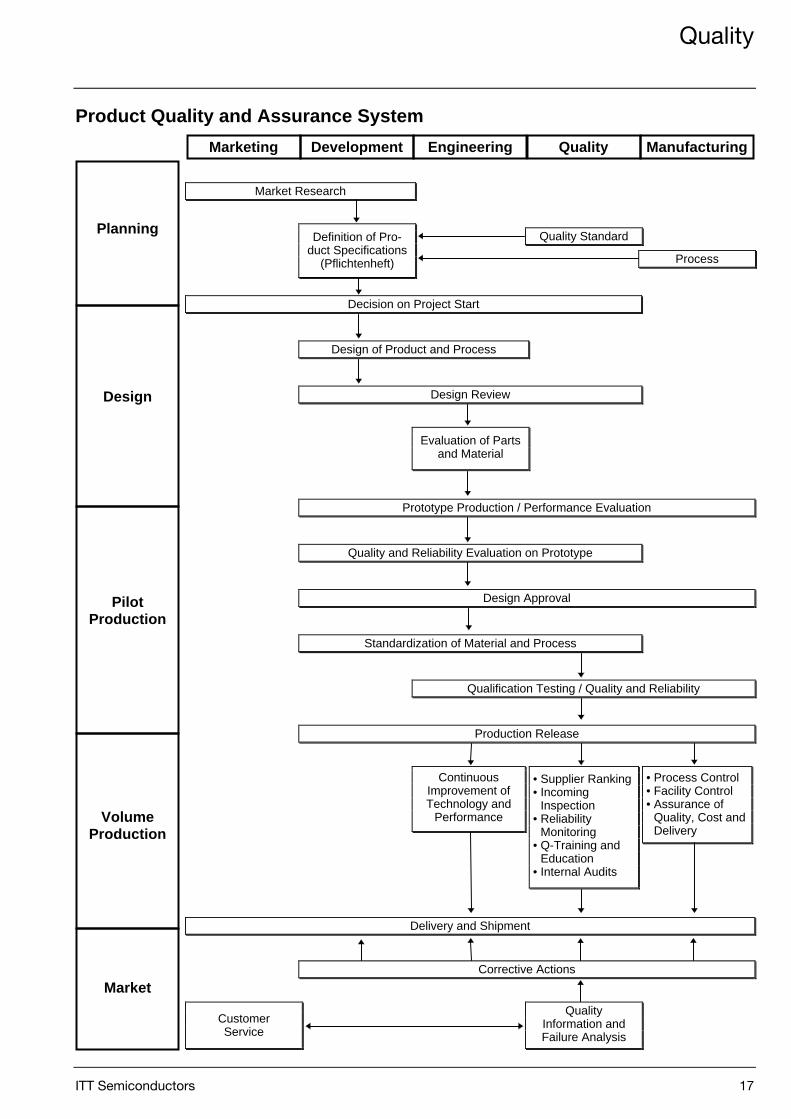
Product Quality and Assurance System
Planning
Design
PilotProduction
VolumeProduction
Market
Marketing Development Engineering Quality Manufacturing
Market Research
Decision on Project Start
Definition of Pro-duct Specifications
(Pflichtenheft)
Quality Standard
Design of Product and Process
Design Review
Evaluation of Partsand Material
Prototype Production / Performance Evaluation
Quality and Reliability Evaluation on Prototype
Design Approval
Qualification Testing / Quality and Reliability
Standardization of Material and Process
Production Release
ContinuousImprovement ofTechnology and
Performance
• Supplier Ranking• Incoming Inspection• Reliability Monitoring• Q-Training and Education• Internal Audits
• Process Control• Facility Control• Assurance of
Quality, Cost andDelivery
Delivery and Shipment
Corrective Actions
CustomerService
QualityInformation andFailure Analysis
Process

18 ITT INTERMETALL
ITT INTERMETALL 19
Small-Signal Transistors (NPN)
20 ITT INTERMETALL
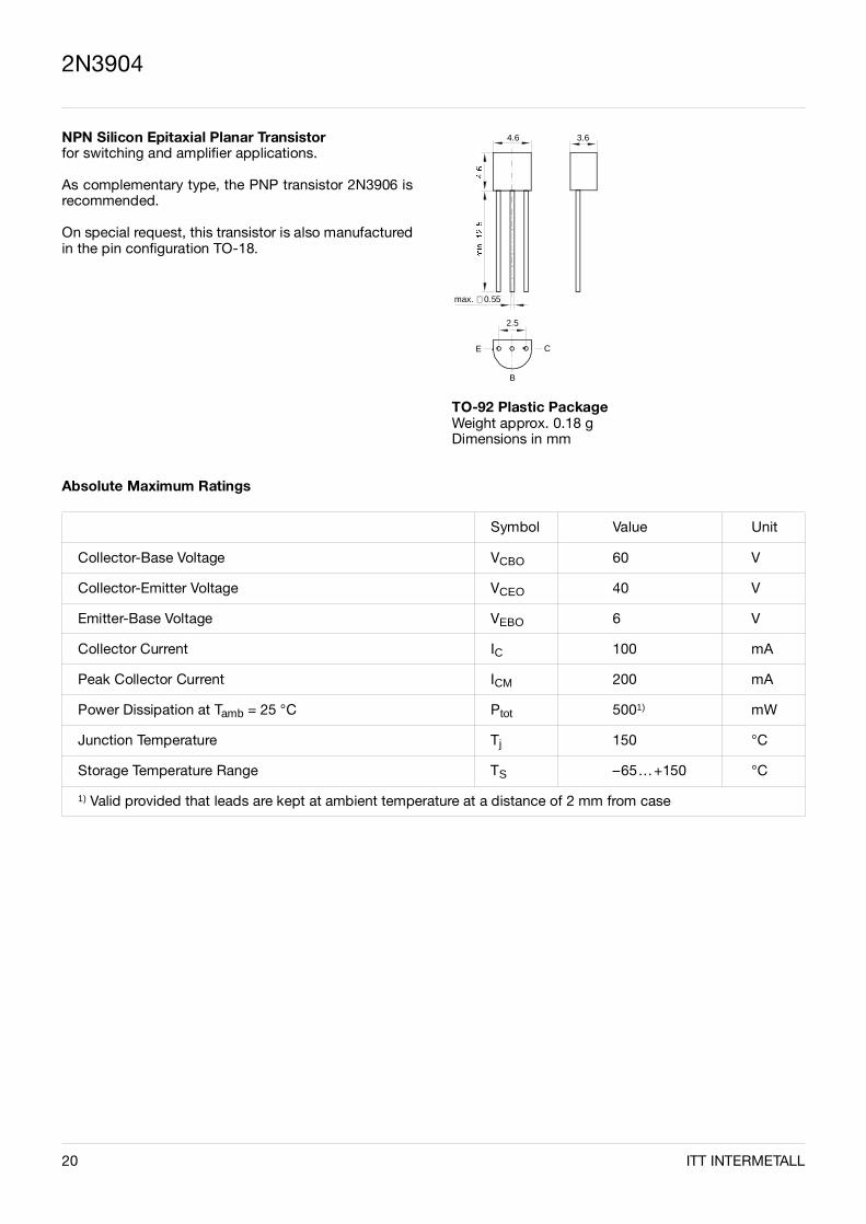
2N3904
NPN Silicon Epitaxial Planar Transistorfor switching and amplifier applications.
As complementary type, the PNP transistor 2N3906 isrecommended.
On special request, this transistor is also manufacturedin the pin configuration TO-18.
Absolute Maximum Ratings
Symbol Value Unit
Collector-Base Voltage VCBO 60 V
Collector-Emitter Voltage VCEO 40 V
Emitter-Base Voltage VEBO 6 V
Collector Current IC 100 mA
Peak Collector Current ICM 200 mA
Power Dissipation at Tamb = 25 °C Ptot 5001) mW
Junction Temperature Tj 150 °C
Storage Temperature Range TS –65…+150 °C
1) Valid provided that leads are kept at ambient temperature at a distance of 2 mm from case
0.55∅ max.
2.5
B
CE
4.6 3.6
TO-92 Plastic PackageWeight approx. 0.18 gDimensions in mm
ITT INTERMETALL 21
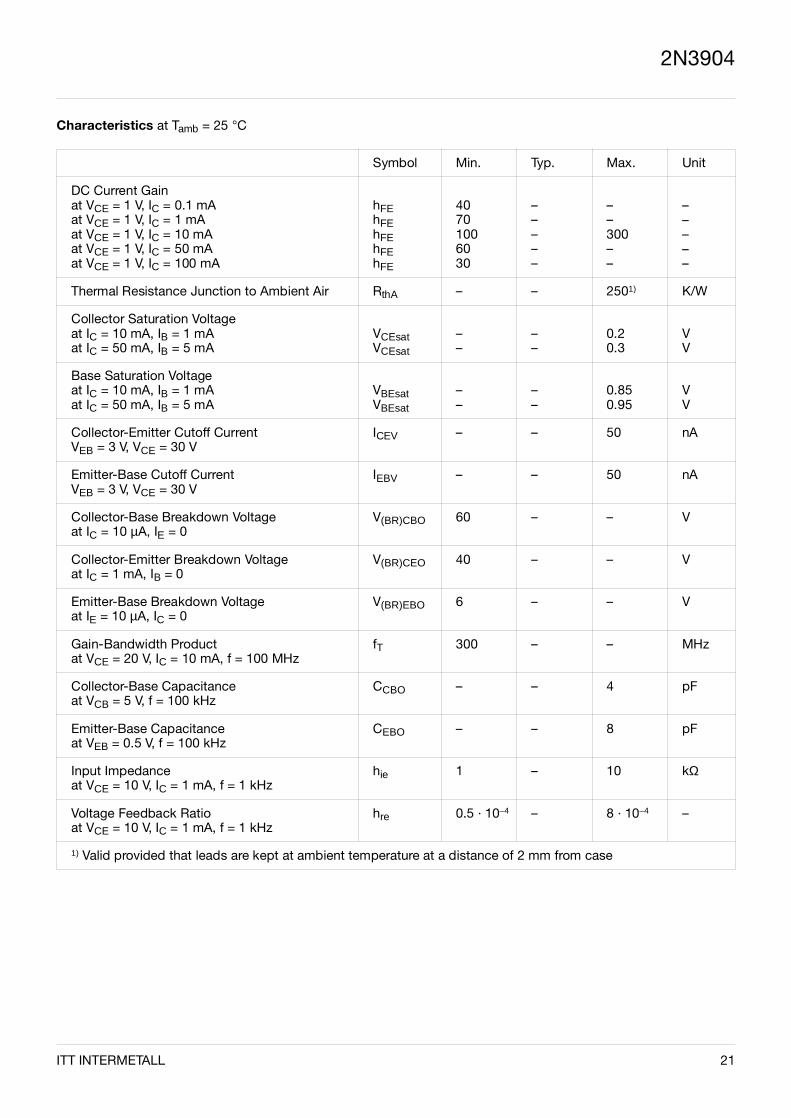
Symbol Min. Typ. Max. Unit
DC Current Gainat VCE = 1 V, IC = 0.1 mAat VCE = 1 V, IC = 1 mAat VCE = 1 V, IC = 10 mAat VCE = 1 V, IC = 50 mAat VCE = 1 V, IC = 100 mA
hFEhFEhFEhFEhFE
40701006030
–––––
––300––
–––––
Thermal Resistance Junction to Ambient Air RthA – – 2501) K/W
Collector Saturation Voltageat IC = 10 mA, IB = 1 mAat IC = 50 mA, IB = 5 mA
VCEsatVCEsat
––
––
0.20.3
VV
Base Saturation Voltageat IC = 10 mA, IB = 1 mAat IC = 50 mA, IB = 5 mA
VBEsatVBEsat
––
––
0.850.95
VV
Collector-Emitter Cutoff CurrentVEB = 3 V, VCE = 30 V
ICEV – – 50 nA
Emitter-Base Cutoff CurrentVEB = 3 V, VCE = 30 V
IEBV – – 50 nA
Collector-Base Breakdown Voltageat IC = 10 µA, IE = 0
V(BR)CBO 60 – – V
Collector-Emitter Breakdown Voltageat IC = 1 mA, IB = 0
V(BR)CEO 40 – – V
Emitter-Base Breakdown Voltageat IE = 10 µA, IC = 0
V(BR)EBO 6 – – V
Gain-Bandwidth Productat VCE = 20 V, IC = 10 mA, f = 100 MHz
fT 300 – – MHz
Collector-Base Capacitanceat VCB = 5 V, f = 100 kHz
CCBO – – 4 pF
Emitter-Base Capacitanceat VEB = 0.5 V, f = 100 kHz
CEBO – – 8 pF
Input Impedanceat VCE = 10 V, IC = 1 mA, f = 1 kHz
hie 1 – 10 kΩ
Voltage Feedback Ratioat VCE = 10 V, IC = 1 mA, f = 1 kHz
hre 0.5 · 10–4 – 8 · 10–4 –
1) Valid provided that leads are kept at ambient temperature at a distance of 2 mm from case
2N3904
Characteristics at Tamb = 25 °C
22 ITT INTERMETALL
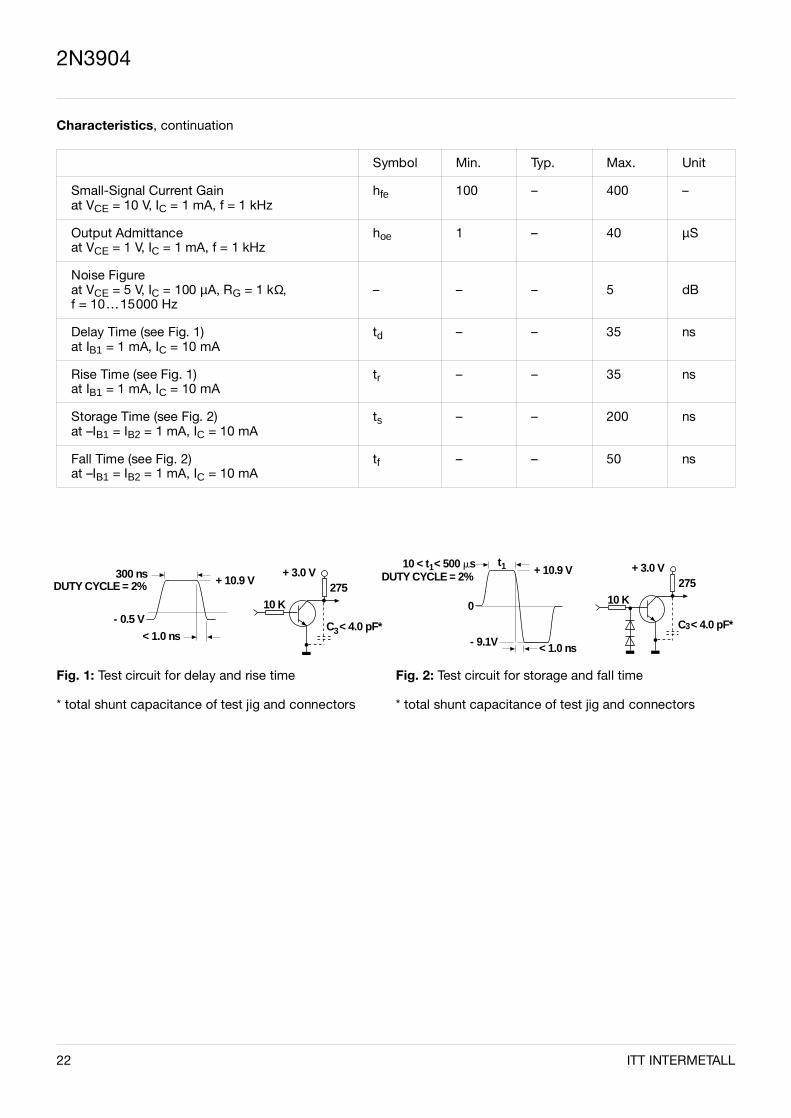
2N3904
Characteristics, continuation
Fig. 1: Test circuit for delay and rise time Fig. 2: Test circuit for storage and fall time
* total shunt capacitance of test jig and connectors * total shunt capacitance of test jig and connectors
Symbol Min. Typ. Max. Unit
Small-Signal Current Gainat VCE = 10 V, IC = 1 mA, f = 1 kHz
hfe 100 – 400 –
Output Admittanceat VCE = 1 V, IC = 1 mA, f = 1 kHz
hoe 1 – 40 µS
Noise Figureat VCE = 5 V, IC = 100 µA, RG = 1 kΩ,f = 10…15000 Hz
– – – 5 dB
Delay Time (see Fig. 1)at IB1 = 1 mA, IC = 10 mA
td – – 35 ns
Rise Time (see Fig. 1)at IB1 = 1 mA, IC = 10 mA
tr – – 35 ns
Storage Time (see Fig. 2)at –IB1 = IB2 = 1 mA, IC = 10 mA
ts – – 200 ns
Fall Time (see Fig. 2)at –IB1 = IB2 = 1 mA, IC = 10 mA
tf – – 50 ns
10 < t < 500 msDUTY CYCLE = 2%
0
+ 10.9 V
- 9.1V
+ 3.0 V275
10 K
C < 4.0 pF*3
t11
< 1.0 ns
300 nsDUTY CYCLE = 2%
- 0.5 V
+ 10.9 V
< 1.0 ns
+ 3.0 V275
10 K
C < 4.0 pF*3

ITT INTERMETALL 23
2N3094

24 ITT INTERMETALL
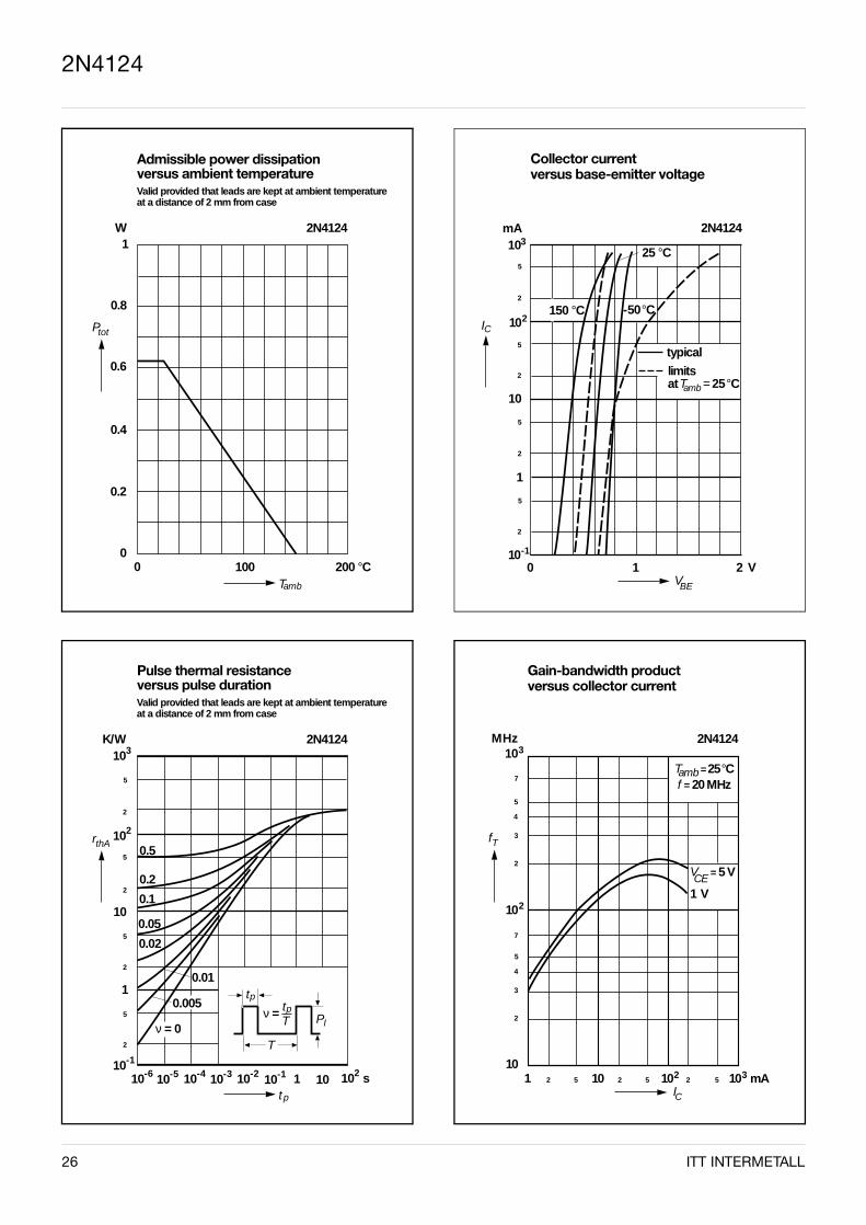
2N4124
NPN Silicon Epitaxial Transistorfor switching and amplifier applications.Especially suitable for AF-driver andlow-power output stages.
As complementary type, the PNP transistor 2N4126 isrecommended.
Absolute Maximum Ratings
Symbol Value Unit
Collector-Emitter Voltage VCEO 25 V
Collector-Base Voltage VCBO 30 V
Emitter-Base Voltage VEBO 5 V
Collector Current IC 200 mA
Peak Collector Current ICM 800 mA
Base Current IB 50 mA
Power Dissipation at Tamb = 25 °C Ptot 6251) mW
Junction Temperature Tj 150 °C
Storage Temperature Range TS –65 to +150 °C
1) Valid provided that leads are kept at ambient temperature at a distance of 2 mm from case.
0.55∅ max.
2.5
B
CE
4.6 3.6
TO-92 Plastic PackageWeight approx. 0.18 gDimensions in mm
ITT INTERMETALL 25
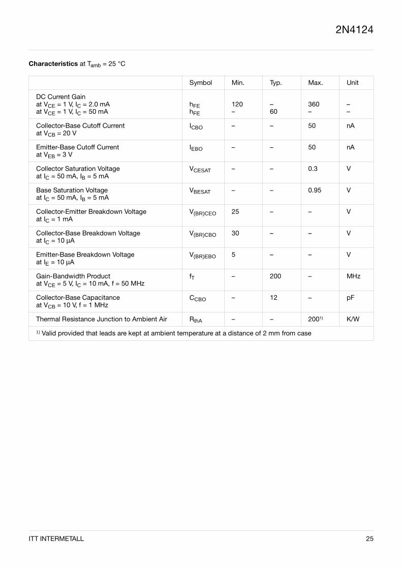
2N4124
Characteristics at Tamb = 25 °C
Symbol Min. Typ. Max. Unit
DC Current Gainat VCE = 1 V, IC = 2.0 mAat VCE = 1 V, IC = 50 mA
hFEhFE
120–
–60
360–
––
Collector-Base Cutoff Currentat VCB = 20 V
ICBO – – 50 nA
Emitter-Base Cutoff Currentat VEB = 3 V
IEBO – – 50 nA
Collector Saturation Voltageat IC = 50 mA, IB = 5 mA
VCESAT – – 0.3 V
Base Saturation Voltageat IC = 50 mA, IB = 5 mA
VBESAT – – 0.95 V
Collector-Emitter Breakdown Voltageat IC = 1 mA
V(BR)CEO 25 – – V
Collector-Base Breakdown Voltageat IC = 10 µA
V(BR)CBO 30 – – V
Emitter-Base Breakdown Voltageat IE = 10 µA
V(BR)EBO 5 – – V
Gain-Bandwidth Productat VCE = 5 V, IC = 10 mA, f = 50 MHz
fT – 200 – MHz
Collector-Base Capacitanceat VCB = 10 V, f = 1 MHz
CCBO – 12 – pF
Thermal Resistance Junction to Ambient Air RthA – – 2001) K/W
1) Valid provided that leads are kept at ambient temperature at a distance of 2 mm from case
26 ITT INTERMETALL
Pulse thermal resistance versus pulse duration
K/W
rthA
1
tp
Valid provided that leads are kept at ambient temperatureat a distance of 2 mm from case
2N4124
2
103
5
102
5
2
10
5
2
5
2
10-1
10-6 10-4 10-2 1 10 s2
0.5
0.2
0.1
0.05
tpν = tp
T PI
T
10-5
ν = 0
0.005
10-3 10-1 10
0.02
0.01
Gain-bandwidth product versus collector current
MHz10
10
IC
3
7
2
2
101
2N4124
5
4
3
7
2
5
4
3
2 5 10 2 5 1022 5 103 mA
Tamb= 25 °Cf = 20 MHz
VCE = 5 V
1 V
fT
Collector current versus base-emitter voltage
mA10
10IC
10
1
VBE
3
5
2
2
5
2
5
2
5
2
10-1
0 1 2 V
2N4124
-50 °C
25 °C
150 °C
typical
at T = 25 °Camb
limits
Admissible power dissipation versus ambient temperature
W1
Ptot
0.6
0.4
10000
0.2
Tamb
200 °C
Valid provided that leads are kept at ambient temperatureat a distance of 2 mm from case
2N4124
0.8
2N4124
ITT INTERMETALL 27
Common emitter collector characteristics
500
400
IC
300
200
100
100
VCE
2 V
I = 0.2 mAB
2N4124
0.8
0.6
0.4
1.4
1.2
1
1.6
1.82
2.4
2.83.2
mA
Base saturation voltage versus collector current
V2
1
10100
I
2N4124
V
I
-1 1 102 310
typical
limitsat
BEsat
= 25 °CTamb
C
IB= 10
150 °C
25 °C
-50 °C
C
mA
-1
DC current gain versus collector current
1000
hFE
100
10
IC
700
500
400
300
200
70
50
40
30
20
10 1 10 102 10 3
2N4124
-50 °C
V = 1 VCE
150 °C
T = 25 °Camb
Collector saturation voltage versus collector current
V0.5
10100
I
2N4124
V
I
-1 1 102 310
typical
limitsat
CEsat
= 25 °CTamb
C
IB= 10
150 °C25 °C
-50 °C
C
mA
0.4
0.3
0.2
0.1
2N4124
28 ITT INTERMETALL
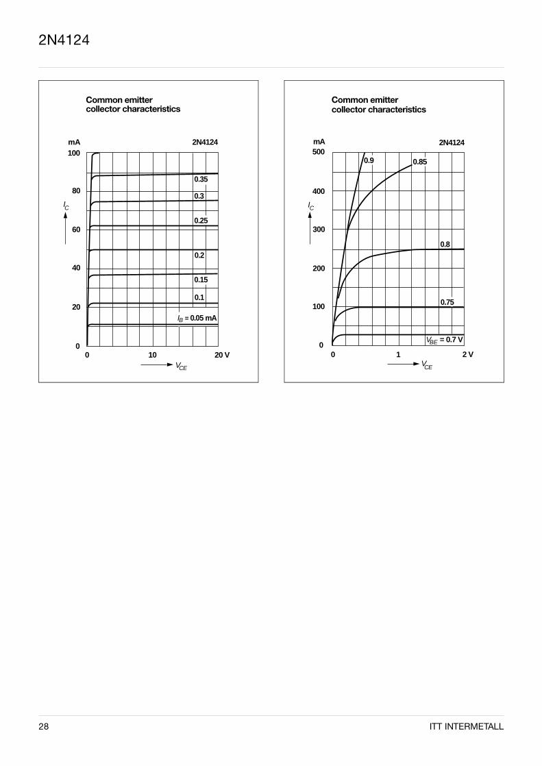
Common emitter collector characteristics
mA100
IC
1000
VCE
20 V
80
60
40
200.1
0.2
0.3
2N4124
I = 0.05 mAB
0.15
0.25
0.35
Common emitter collector characteristics
mA500
400
IC
300
200
100
100
VCE
2 V
0.8
2N4124
0.75
0.850.9
V = 0.7 VBE
2N4124

ITT INTERMETALL 29
2N4124

30 ITT INTERMETALL
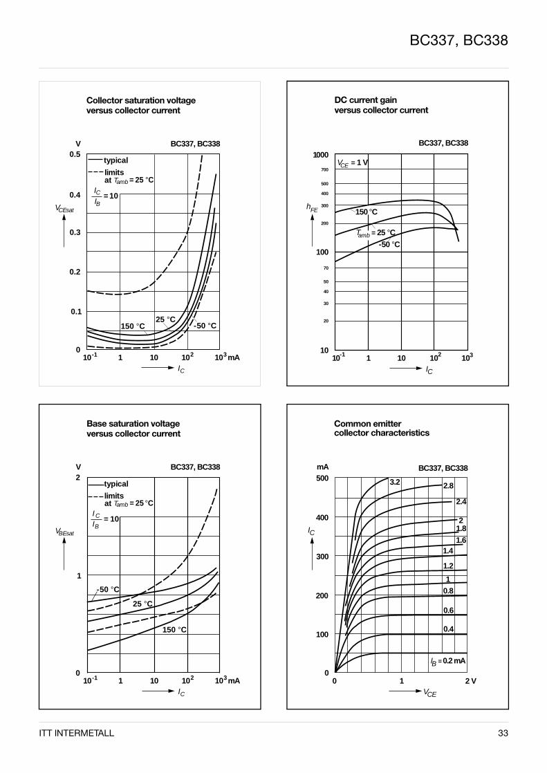
BC337, BC338
NPN Silicon Epitaxial Planar Transistorsfor switching and amplifier applications. Especially suit-able for AF-driver stages and low power output stages.
These types are also available subdivided into threegroups -16, -25, and -40, according to their DC currentgain. As complementary types, the PNP transistorsBC327 and BC328 are recommended.
On special request, these transistors are also manu-factured in the pin configuration TO-18.
Absolute Maximum Ratings
Symbol Value Unit
Collector-Emitter Voltage BC337BC338
VCESVCES
5030
VV
Collector-Emitter Voltage BC337BC338
VCEOVCEO
4525
VV
Emitter-Base Voltage VEBO 5 V
Collector Current IC 800 mA
Peak Collector Current ICM 1 A
Base Current IB 100 mA
Power Dissipation at Tamb = 25 °C Ptot 6251) mW
Junction Temperature Tj 150 °C
Storage Temperature Range TS –65 to +150 °C
1) Valid provided that leads are kept at ambient temperature at a distance of 2 mm from case
0.55∅ max.
2.5
B
EC
4.6 3.6
TO-92 Plastic PackageWeight approx. 0.18 gDimensions in mm
ITT INTERMETALL 31
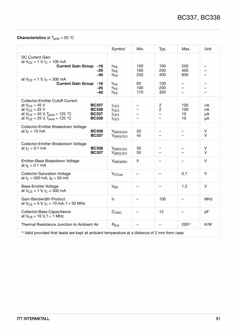
BC337, BC338
Characteristics at Tamb = 25 °C
Symbol Min. Typ. Max. Unit
DC Current Gainat VCE = 1 V, IC = 100 mA
Current Gain Group -16-25-40
at VCE = 1 V, IC = 300 mACurrent Gain Group -16
-25-40
hFEhFEhFE
hFEhFEhFE
100160250
60100170
160250400
130200320
250400630
–––
–––
–––
Collector-Emitter Cutoff Currentat VCE = 45 V BC337at VCE = 25 V BC338at VCE = 45 V, Tamb = 125 °C BC337at VCE = 25 V, Tamb = 125 °C BC338
ICESICESICESICES
––––
22––
1001001010
nAnAµAµA
Collector-Emitter Breakdown Voltageat IC = 10 mA BC338
BC337V(BR)CEOV(BR)CEO
2045
––
––
VV
Collector-Emitter Breakdown Voltageat IC = 0.1 mA BC338
BC337V(BR)CESV(BR)CES
3050
––
––
VV
Emitter-Base Breakdown Voltageat IE = 0.1 mA
V(BR)EBO 5 – – V
Collector Saturation Voltageat IC = 500 mA, IB = 50 mA
VCEsat – – 0.7 V
Base-Emitter Voltageat VCE = 1 V, IC = 300 mA
VBE – – 1.2 V
Gain-Bandwidth Productat VCE = 5 V, IC = 10 mA, f = 50 MHz
fT – 100 – MHz
Collector-Base Capacitanceat VCB = 10 V, f = 1 MHz
CCBO – 12 – pF
Thermal Resistance Junction to Ambient Air RthA – – 2001) K/W
1) Valid provided that leads are kept at ambient temperature at a distance of 2 mm from case
ITT INTERMETALL 31

32 ITT INTERMETALL
BC337, BC338
Admissible power dissipation versus ambient temperature
W1
Ptot
0.6
0.4
10000
0.2
Tamb
200 °C
Valid provided that leads are kept at ambient temperatureat a distance of 2 mm from case
BC337, BC338
0.8
Pulse thermal resistance versus pulse duration
K/W
rthA
1
tp
Valid provided that leads are kept at ambient temperatureat a distance of 2 mm from case
BC337, BC338
2
103
5
102
5
2
10
5
2
5
2
10-1
10-6 10-4 10-2 1 10 s2
0.5
0.2
0.1
0.05
tpν = tp
T PI
T
10-5
ν = 0
0.005
10-3 10-1 10
0.02
0.01
Collector current versus base-emitter voltage
mA10
10IC
10
1
VBE
3
5
2
2
5
2
5
2
5
2
10-1
0 1 2 V
BC337, BC338
-50 °C
25 °C
150 °C
typical
at T = 25 °Camb
limits
Gain-bandwidth product versus collector current
MHz10
10
IC
3
7
2
2
101
BC337, BC338
5
4
3
7
2
5
4
3
2 5 10 2 5 1022 5 103 mA
Tamb= 25 °Cf = 20 MHz
VCE = 5 V
1 V
fT
ITT INTERMETALL 33
BC337, BC338
Collector saturation voltage versus collector current
V0.5
10100
I
BC337, BC338
V
I
-1 1 102 310
typical
limitsat
CEsat
= 25 °CTamb
C
IB= 10
150 °C25 °C
-50 °C
C
mA
0.4
0.3
0.2
0.1
Base saturation voltage versus collector current
V2
1
10100
I
BC337, BC338
V
I
-1 1 102 310
typical
limitsat
BEsat
= 25 °CTamb
C
IB= 10
150 °C
25 °C
-50 °C
C
mA
-1
DC current gain versus collector current
1000
hFE
100
10
IC
700
500
400
300
200
70
50
40
30
20
10 1 10 102 10 3
BC337, BC338
-50 °C
V = 1 VCE
150 °C
T = 25 °Camb
Common emitter collector characteristics
500
400
IC
300
200
100
100
VCE
2 V
I = 0.2 mAB
BC337, BC338
0.8
0.6
0.4
1.4
1.2
1
1.6
1.82
2.4
2.83.2
mA
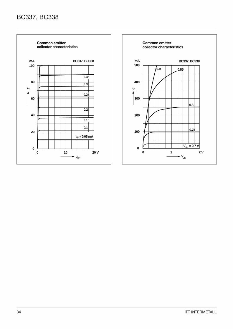
34 ITT INTERMETALL
BC337, BC338
Common emitter collector characteristics
mA100
IC
1000
VCE
20 V
80
60
40
200.1
0.2
0.3
BC337, BC338
I = 0.05 mAB
0.15
0.25
0.35
Common emitter collector characteristics
mA500
400
IC
300
200
100
100
VCE
2 V
0.8
BC337, BC338
0.75
0.850.9
V = 0.7 VBE

ITT INTERMETALL 35
BC337, BC338
36 ITT INTERMETALL
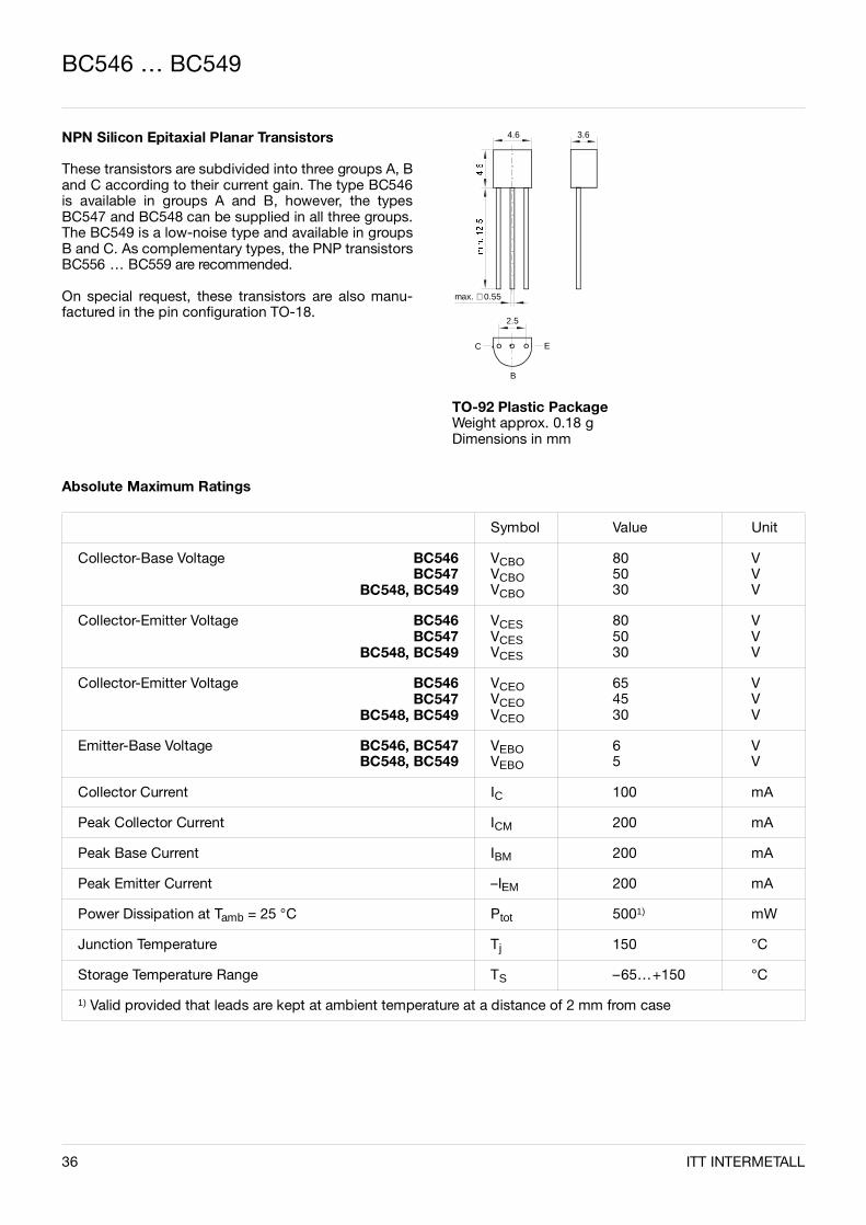
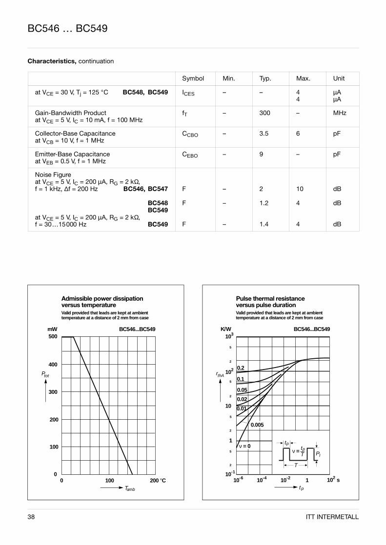
BC546 … BC549
NPN Silicon Epitaxial Planar Transistors
These transistors are subdivided into three groups A, Band C according to their current gain. The type BC546is available in groups A and B, however, the typesBC547 and BC548 can be supplied in all three groups.The BC549 is a low-noise type and available in groupsB and C. As complementary types, the PNP transistorsBC556 … BC559 are recommended.
On special request, these transistors are also manu-factured in the pin configuration TO-18.
Absolute Maximum Ratings
Symbol Value Unit
Collector-Base Voltage BC546BC547
BC548, BC549
VCBOVCBOVCBO
805030
VVV
Collector-Emitter Voltage BC546BC547
BC548, BC549
VCESVCESVCES
805030
VVV
Collector-Emitter Voltage BC546BC547
BC548, BC549
VCEOVCEOVCEO
654530
VVV
Emitter-Base Voltage BC546, BC547BC548, BC549
VEBOVEBO
65
VV
Collector Current IC 100 mA
Peak Collector Current ICM 200 mA
Peak Base Current IBM 200 mA
Peak Emitter Current –IEM 200 mA
Power Dissipation at Tamb = 25 °C Ptot 5001) mW
Junction Temperature Tj 150 °C
Storage Temperature Range TS –65…+150 °C
1) Valid provided that leads are kept at ambient temperature at a distance of 2 mm from case
0.55∅ max.
2.5
B
EC
4.6 3.6
TO-92 Plastic PackageWeight approx. 0.18 gDimensions in mm
ITT INTERMETALL 37
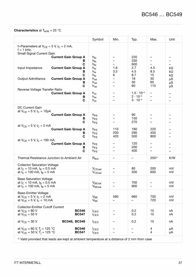
BC546 … BC549
Characteristics at Tamb = 25 °C
Symbol Min. Typ. Max. Unit
h-Parameters at VCE = 5 V, IC = 2 mA,f = 1 kHz,Small Signal Current Gain
Current Gain Group ABC
Input Impedance Current Gain Group ABC
Output Admittance Current Gain Group ABC
Reverse Voltage Transfer RatioCurrent Gain Group A
BC
hfehfehfehiehiehiehoehoehoe
hrehrehre
–––1.63.26–––
–––
2203306002.74.58.7183060
1.5 · 10–4
2 · 10–4
3 · 10–4
–––4.58.5153060110
–––
–––kΩkΩkΩµSµSµS
–––
DC Current Gainat VCE = 5 V, IC = 10µA
Current Gain Group ABC
at VCE = 5 V, IC = 2 mACurrent Gain Group A
BC
at VCE = 5 V, IC = 100 mACurrent Gain Group A
BC
hFEhFEhFE
hFEhFEhFE
hFEhFEhFE
–––
110200420
–––
90150270
180290500
120200400
–––
220450800
–––
–––
–––
–––
Thermal Resistance Junction to Ambient Air RthA – – 2501) K/W
Collector Saturation Voltageat IC = 10 mA, IB = 0.5 mAat IC = 100 mA, IB = 5 mA
VCEsatVCEsat
––
80200
200600
mVmV
Base Saturation Voltageat IC = 10 mA, IB = 0.5 mAat IC = 100 mA, IB = 5 mA
VBEsatVBEsat
––
700900
––
mVmV
Base-Emitter Voltageat VCE = 5 V, IC = 2 mAat VCE = 5 V, IC = 10 mA
VBEVBE
580–
660–
700720
mVmV
Collector-Emitter Cutoff Currentat VCE = 80 V BC546at VCE = 50 V BC547
at VCE = 30 V BC548, BC549
at VCE = 80 V, Tj = 125 °C BC546at VCE = 50 V, Tj = 125 °C BC547
ICESICES
ICES
ICESICES
––
–
––
0.20.2
0.2
––
1515
15
44
nAnA
nA
µAµA
1) Valid provided that leads are kept at ambient temperature at a distance of 2 mm from case
38 ITT INTERMETALL
Symbol Min. Typ. Max. Unit
at VCE = 30 V, Tj = 125 °C BC548, BC549 ICES – – 44
µAµA
Gain-Bandwidth Productat VCE = 5 V, IC = 10 mA, f = 100 MHz
fT – 300 – MHz
Collector-Base Capacitanceat VCB = 10 V, f = 1 MHz
CCBO – 3.5 6 pF
Emitter-Base Capacitanceat VEB = 0.5 V, f = 1 MHz
CEBO – 9 – pF
Noise Figureat VCE = 5 V, IC = 200 µA, RG = 2 kΩ,f = 1 kHz, ∆f = 200 Hz BC546, BC547
BC548BC549
at VCE = 5 V, IC = 200 µA, RG = 2 kΩ,f = 30…15000 Hz BC549
F
F
F
–
–
–
2
1.2
1.4
10
4
4
dB
dB
dB
BC546 … BC549
Admissible power dissipation versus temperature
mW500
Ptot
300
200
10000
100
Tamb
200 °C
Valid provided that leads are kept at ambienttemperature at a distance of 2 mm from case
BC546...BC549
400
Pulse thermal resistance versus pulse duration
K/W
rthA
1
tp
Valid provided that leads are kept at ambienttemperature at a distance of 2 mm from case
BC546...BC549
2
103
5
102
5
2
10
5
2
5
2
10-1
10-6 10-4 10-2 1 10 s2
0.2
0.1
0.05
0.02
0.01
0.005
tpν = tp
T PI
T
ν = 0
Characteristics, continuation
ITT INTERMETALL 39
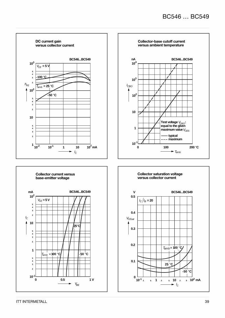
BC546 … BC549
DC current gain versus collector current
10
5
hFE
101
IC
3BC546...BC549
4
3
2
102
5
4
3
2
10
54
3
2
-2 10-1 101 102 mA
-50 °C
VCE = 5 V
100 °C
Tamb = 25 °C
Collector current versus base-emitter voltage
mA10
5
IC
10
1
010
VBE
BC546...BC5492
4
3
2
5
4
3
2
5
4
3
2
-1
0.5 1 V
Tamb = 100 °C -50 °C
25 °C
VCE = 5 V
Collector-base cutoff current versus ambient temperature
nA
ICBO
10
1000
1
Tamb
200 °C
BC546...BC549
103
104
102
10-1
Test voltage V :equal to the givenmaximum value
typicalmaximum
VCES
CBO
Collector saturation voltage versus collector current
V0.5
0.4
VCEsat
0.3
0.2
10
0.1
IC
BC546...BC549
102 5 2 5 2 510-1 10 mA2
-50 °C
25 °C
Tamb= 100 °C
I C = 20I B
40 ITT INTERMETALL
Noise figure versus collector current
dB20
F
12
8
100
6
IC10 mA
BC549
18
16
14
10
4
2
-3 10-2 10-1 1
V = 5 VCE
f = 120 Hz
amb
G
500 V
1kV
T = 25 °C
R = 1 MV 100 kV 10 kV 1 kV
BC546 … BC549
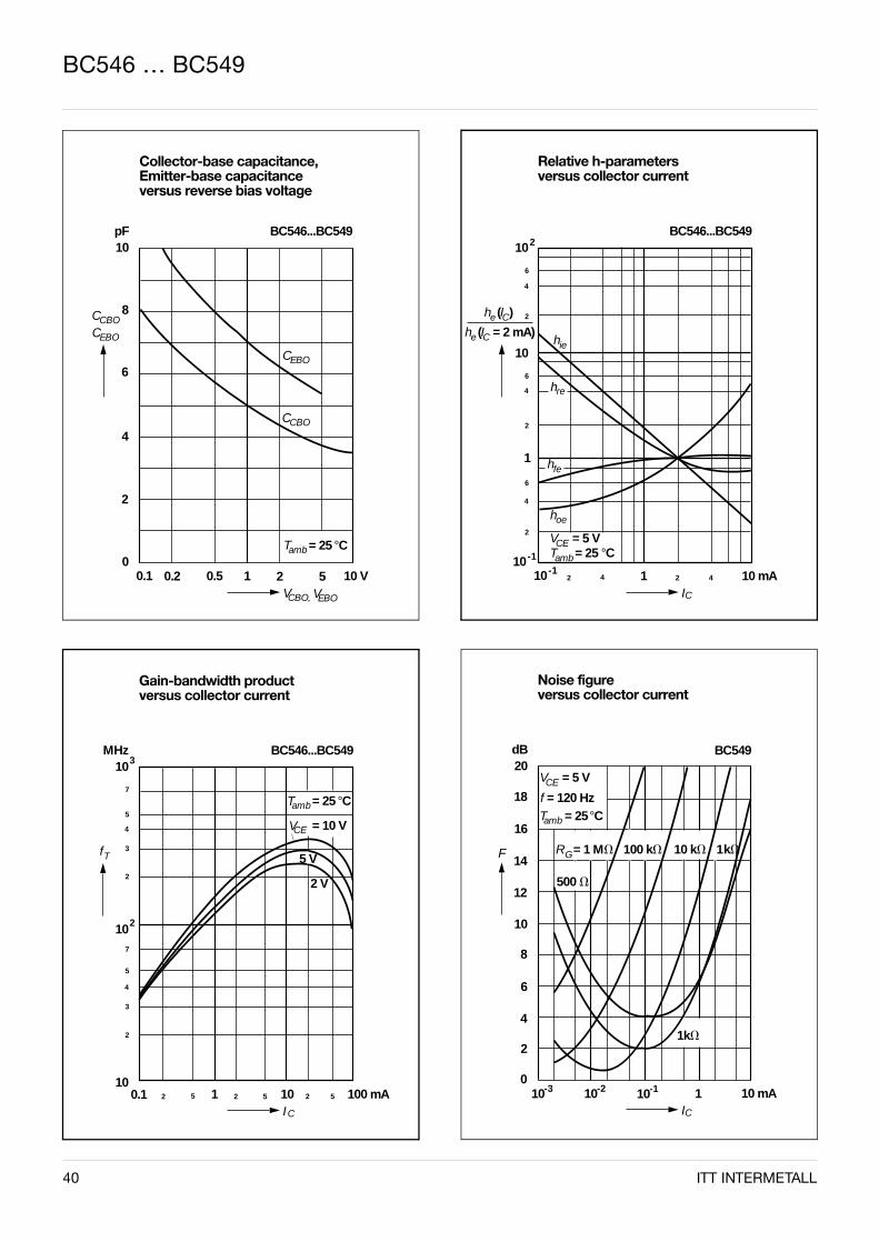
Collector-base capacitance, Emitter-base capacitance versus reverse bias voltage
pF10
6
4
10.10
2
VCBO,
10 V
BC546...BC549
8
VEBO
0.2 0.5 2 5
CCBOCEBO
CCBO
CEBO
T = 25 °Camb
Gain-bandwidth product versus collector current
MHz10
fT
0.1IC
100 mA
BC546...BC5493
7
5
4
3
2
102
7
5
4
3
2
102 5 1 2 5 10 2 5
T = 25 °Camb
V = 10 VCE
5 V
2 V
Relative h-parameters versus collector current
10
110
1
IC10 mA
BC546...BC549102
6
4
2
6
4
2
6
4
2
-1
10-12 4 2 4
h (I = 2 mA)e C
h (I )e C
hie
hoe
hre
hfe
V = 5 VCET = 25 °Camb
ITT INTERMETALL 41
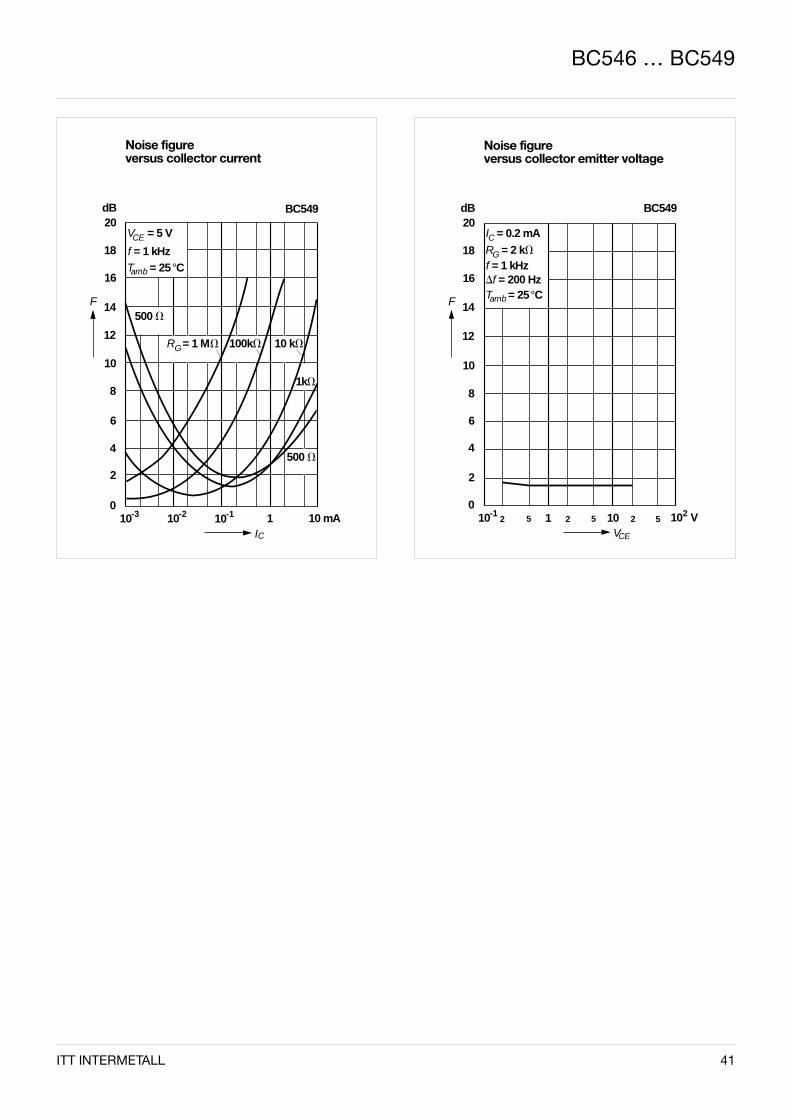
BC546 … BC549
Noise figure versus collector current
dB20
F
12
8
100
6
IC10 mA
BC549
18
16
14
10
4
2
-3 10-2 10-1 1
V = 5 VCE
f = 1 kHz
amb
500 V
1kV
500 V
T = 25 °C
GR = 1 MV 100kV 10 kV
Noise figure versus collector emitter voltage
dB20
F
12
8
100
6
VCE
10 V
BC549
18
16
14
10
4
2
-12 1 2
I = 0.2 mAC
f = 1 kHz
ambT = 25 °C
R = 2 kVG
Df = 200 Hz
5 5 10 2 52
42 ITT INTERMETALL
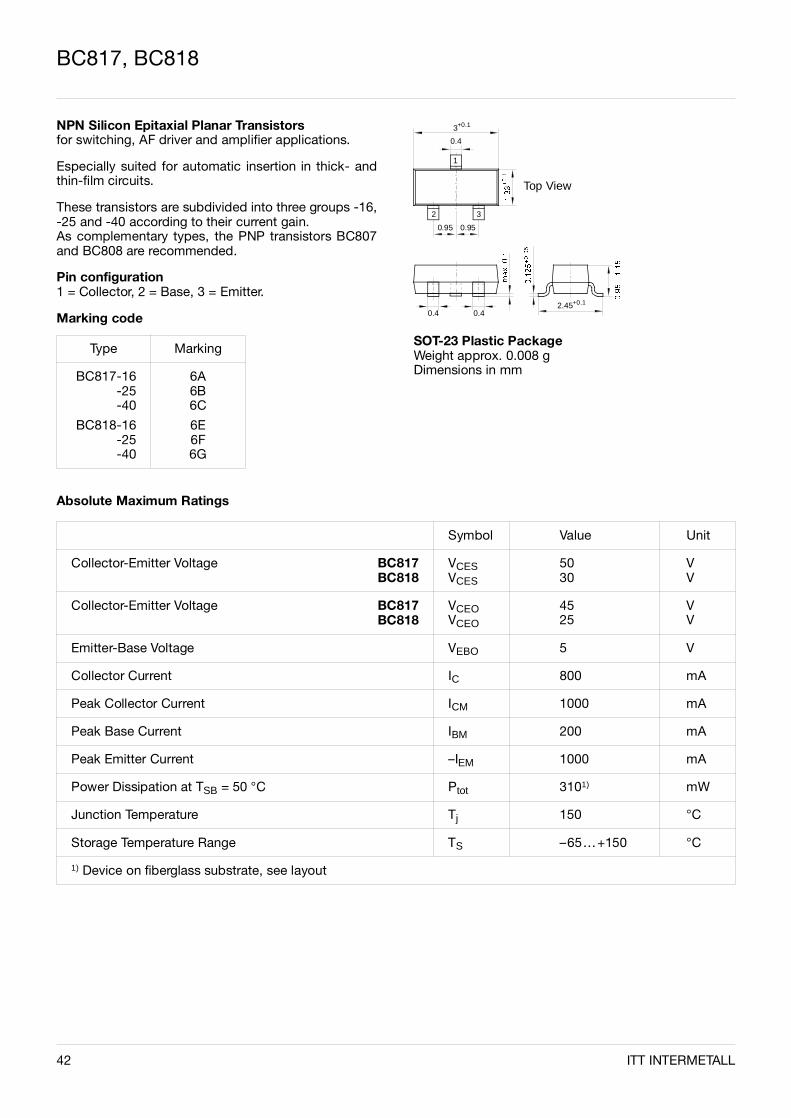
BC817, BC818
NPN Silicon Epitaxial Planar Transistorsfor switching, AF driver and amplifier applications.
Especially suited for automatic insertion in thick- andthin-film circuits.
These transistors are subdivided into three groups -16,-25 and -40 according to their current gain.As complementary types, the PNP transistors BC807and BC808 are recommended.
Pin configuration1 = Collector, 2 = Base, 3 = Emitter.
Marking code
Type Marking
BC817-16-25-40
BC818-16-25-40
6A6B6C
6E6F6G
Absolute Maximum Ratings
Symbol Value Unit
Collector-Emitter Voltage BC817BC818
VCESVCES
5030
VV
Collector-Emitter Voltage BC817BC818
VCEOVCEO
4525
VV
Emitter-Base Voltage VEBO 5 V
Collector Current IC 800 mA
Peak Collector Current ICM 1000 mA
Peak Base Current IBM 200 mA
Peak Emitter Current –IEM 1000 mA
Power Dissipation at TSB = 50 °C Ptot 3101) mW
Junction Temperature Tj 150 °C
Storage Temperature Range TS –65…+150 °C
1) Device on fiberglass substrate, see layout
0.4
0.95 0.95
3
0.4 0.4
+0.1
1
2 3
Top View
SOT-23 Plastic PackageWeight approx. 0.008 gDimensions in mm
2.45+0.1
ITT INTERMETALL 43
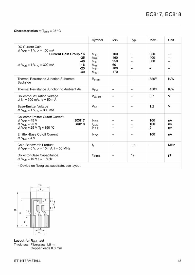
BC817, BC818
Characteristics at Tamb = 25 °C
Symbol Min. Typ. Max. Unit
DC Current Gainat VCE = 1 V, IC = 100 mA
Current Gain Group-16-25-40
at VCE = 1 V, IC = 300 mA -16-25-40
hFEhFEhFEhFEhFEhFE
10016025060100170
––––––
250400600–––
––––––
Thermal Resistance Junction SubstrateBackside
RthSB – – 3201) K/W
Thermal Resistance Junction to Ambient Air RthA – – 4501) K/W
Collector Saturation Voltageat IC = 500 mA, IB = 50 mA
VCEsat – – 0.7 V
Base-Emitter Voltageat VCE = 1 V, IC = 300 mA
VBE – – 1.2 V
Collector-Emitter Cutoff Currentat VCE = 45 V BC817at VCE = 25 V BC818at VCE = 25 V, Tj = 150 °C
ICESICESICES
–––
–––
1001005
nAnAµA
Emitter-Base Cutoff Currentat VEB = 4 V
IEBO – – 100 nA
Gain-Bandwidth Productat VCE = 5 V, IC = 10 mA, f = 50 MHz
fT – 100 – MHz
Collector-Base Capacitanceat VCB = 10 V, f = 1 MHz
CCBO – 12 pF
1) Device on fiberglass substrate, see layout
Layout for RthA testThickness: Fiberglass 1.5 mm
Copper leads 0.3 mm
15 12
5
0.8
7.5
3
1
1.5
5.1
2
2
1

44 ITT INTERMETALL
BC817, BC818
Admissible power dissipation versus temperature of substrate backside
mW500
Ptot
300
200
10000
100
TSB
200 °C
Device on fiberglass substrate, see layout
BC817, BC818
400
Pulse thermal resistance versus pulse duration (normalized)
10
10
RthSB
tp
Device on fiberglass substrate, see layout
0
5
3
-1
5
2
4
2
10-3
10-7 10-6 10-5 10-4 10-3 10-2 1 s
BC817, BC818
tptpT
ν =PI
T
0.1
0.05
0.02
0.01
ν = 0
4
2
4
3
5
3
10-1
5 -3
0.2
0.5
rthSB
10-2
Collector current versus base-emitter voltage
mA10
10IC
10
1
VBE
3
5
2
2
5
2
5
2
5
2
10-1
0 1 2 V
BC817, BC818
-50 °C
25 °C
typical
at T =25 °Camblimits
150 °C
Gain-bandwidth product versus collector current
MHz10
10
IC
3
7
2
2
101
BC817, BC818
5
4
3
7
2
5
4
3
2 5 10 2 5 1022 5 103 mA
Tamb = 25 °Cf = 20 MHz
VCE = 5 V
1 V
fT

ITT INTERMETALL 45
BC817, BC818
Collector saturation voltage versus collector current
V0.5
10100
I
BC817, BC818
V
I
-1 1 102 310
typical
limitsat
CEsat
= 25 °CTamb
C
IB= 10
150 °C25 °C
-50 °C
C
mA
0.4
0.3
0.2
0.1
Base saturation voltage versus collector current
V2
1
10100
I
BC817, BC818
V
I
-1 1 102 310
typical
limitsat
BEsat
= 25 °CTamb
CIB
= 10
150 °C
25 °C
-50 °C
C
mA
-1
DC current gain versus collector current
1000
hFE
100
10
IC
700
500
400
300
200
70
50
40
30
20
10 1 10 102 10 mA3
BC817, BC818
-50 °C
V =1 VCE
150 °C
T = 25 °Camb
Common emitter collector characteristics
500
400
IC
300
200
100
100
VCE
2 V
I = 0.2 mAB
BC817, BC818
0.8
0.6
0.4
1.4
1.2
1
1.6
1.82
2.4
2.83.2
mA
46 ITT INTERMETALL
BC817, BC818
Common emitter collector characteristics
mA100
IC
1000
VCE
20 V
80
60
40
200.1
0.2
0.3
BC817, BC818
I = 0.05 mAB
0.15
0.25
0.35
Common emitter collector characteristics
mA500
400
IC
300
200
100
100
VCE
2 V
0.8
BC817, BC818
0.75
0.850.9
V = 0.7 VBE

ITT INTERMETALL 47
BC817, BC818
48 ITT INTERMETALL
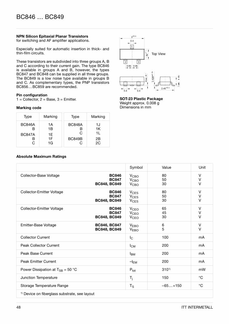
BC846 … BC849
NPN Silicon Epitaxial Planar Transistorsfor switching and AF amplifier applications.
Especially suited for automatic insertion in thick- andthin-film circuits.
These transistors are subdivided into three groups A, Band C according to their current gain. The type BC846is available in groups A and B, however, the typesBC847 and BC848 can be supplied in all three groups.The BC849 is a low noise type available in groups Band C. As complementary types, the PNP transistorsBC856…BC859 are recommended.
Pin configuration1 = Collector, 2 = Base, 3 = Emitter.
Marking code
Type Marking
BC846AB
BC847ABC
1A1B
1E1F1G
Absolute Maximum Ratings
Symbol Value Unit
Collector-Base Voltage BC846BC847
BC848, BC849
VCBOVCBOVCBO
805030
VVV
Collector-Emitter Voltage BC846BC847
BC848, BC849
VCESVCESVCES
805030
VVV
Collector-Emitter Voltage BC846BC847
BC848, BC849
VCEOVCEOVCEO
654530
VVV
Emitter-Base Voltage BC846, BC847BC848, BC849
VEBOVEBO
65
VV
Collector Current IC 100 mA
Peak Collector Current ICM 200 mA
Peak Base Current IBM 200 mA
Peak Emitter Current –IEM 200 mA
Power Dissipation at TSB = 50 °C Ptot 3101) mW
Junction Temperature Tj 150 °C
Storage Temperature Range TS –65…+150 °C
1) Device on fiberglass substrate, see layout
Type Marking
BC848ABC
BC849BC
1J1K1L
2B2C
0.4
0.95 0.95
3
0.4 0.4
+0.1
1
2 3
Top View
SOT-23 Plastic PackageWeight approx. 0.008 gDimensions in mm
2.45+0.1
ITT INTERMETALL 49
BC846 … BC849
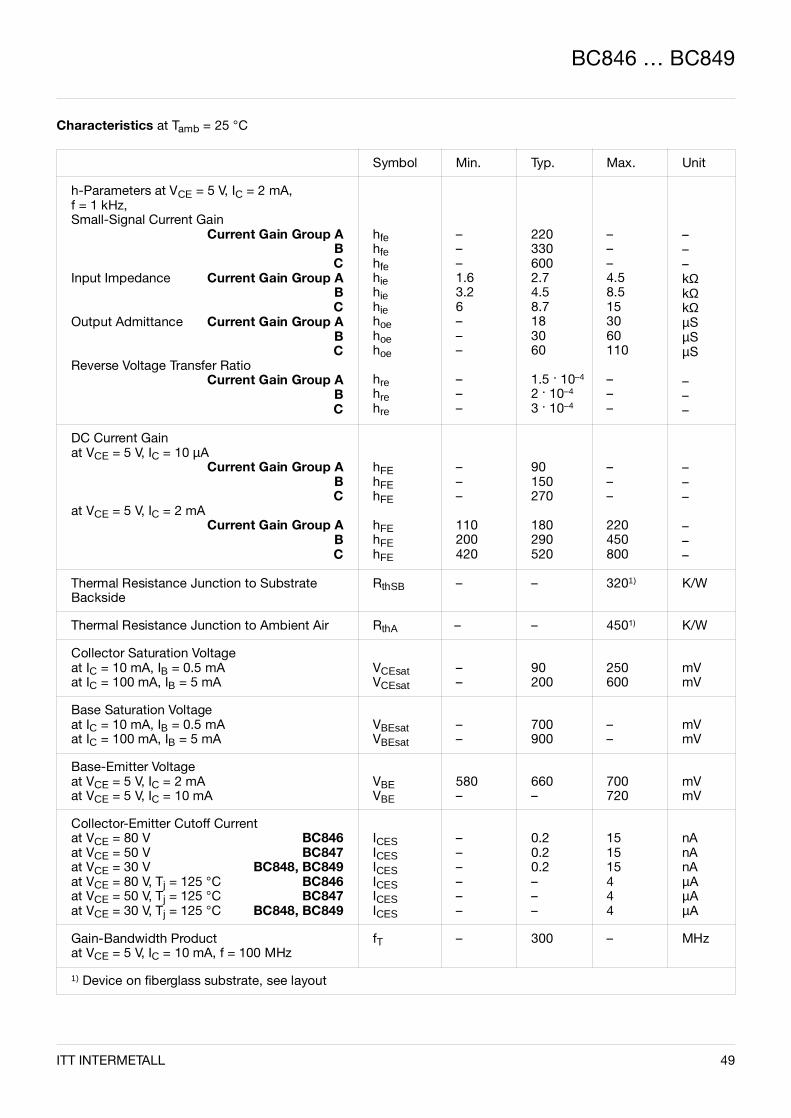
Characteristics at Tamb = 25 °C
Symbol Min. Typ. Max. Unit
h-Parameters at VCE = 5 V, IC = 2 mA,f = 1 kHz, Small-Signal Current Gain
Current Gain Group ABC
Input Impedance Current Gain Group ABC
Output Admittance Current Gain Group ABC
Reverse Voltage Transfer RatioCurrent Gain Group A
BC
hfehfehfehiehiehiehoehoehoe
hrehrehre
–––1.63.26–––
–––
2203306002.74.58.7183060
1.5 · 10–4
2 · 10–4
3 · 10–4
–––4.58.5153060110
–––
–––kΩkΩkΩµSµSµS
–––
DC Current Gainat VCE = 5 V, IC = 10 µA
Current Gain Group ABC
at VCE = 5 V, IC = 2 mACurrent Gain Group A
BC
hFEhFEhFE
hFEhFEhFE
–––
110200420
90150270
180290520
–––
220450800
–––
–––
Thermal Resistance Junction to SubstrateBackside
RthSB – – 3201) K/W
Thermal Resistance Junction to Ambient Air RthA – – 4501) K/W
Collector Saturation Voltageat IC = 10 mA, IB = 0.5 mAat IC = 100 mA, IB = 5 mA
VCEsatVCEsat
––
90200
250600
mVmV
Base Saturation Voltageat IC = 10 mA, IB = 0.5 mAat IC = 100 mA, IB = 5 mA
VBEsatVBEsat
––
700900
––
mVmV
Base-Emitter Voltageat VCE = 5 V, IC = 2 mAat VCE = 5 V, IC = 10 mA
VBEVBE
580–
660–
700720
mVmV
Collector-Emitter Cutoff Currentat VCE = 80 V BC846at VCE = 50 V BC847at VCE = 30 V BC848, BC849at VCE = 80 V, Tj = 125 °C BC846at VCE = 50 V, Tj = 125 °C BC847at VCE = 30 V, Tj = 125 °C BC848, BC849
ICESICESICESICESICESICES
––––––
0.20.20.2–––
151515444
nAnAnAµAµAµA
Gain-Bandwidth Productat VCE = 5 V, IC = 10 mA, f = 100 MHz
fT – 300 – MHz
1) Device on fiberglass substrate, see layout
50 ITT INTERMETALL
BC846 … BC849
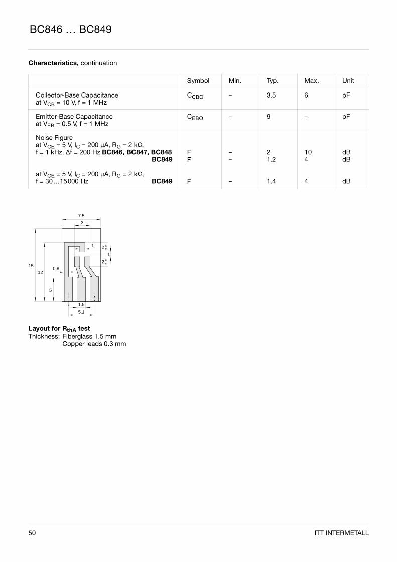
Symbol Min. Typ. Max. Unit
Collector-Base Capacitanceat VCB = 10 V, f = 1 MHz
CCBO – 3.5 6 pF
Emitter-Base Capacitanceat VEB = 0.5 V, f = 1 MHz
CEBO – 9 – pF
Noise Figureat VCE = 5 V, IC = 200 µA, RG = 2 kΩ,f = 1 kHz, ∆f = 200 Hz BC846, BC847, BC848
BC849
at VCE = 5 V, IC = 200 µA, RG = 2 kΩ,f = 30…15000 Hz BC849
FF
F
––
–
21.2
1.4
104
4
dBdB
dB
Characteristics, continuation
Layout for RthA testThickness: Fiberglass 1.5 mm
Copper leads 0.3 mm
15 12
5
0.8
7.5
3
1
1.5
5.1
2
2
1
ITT INTERMETALL 51
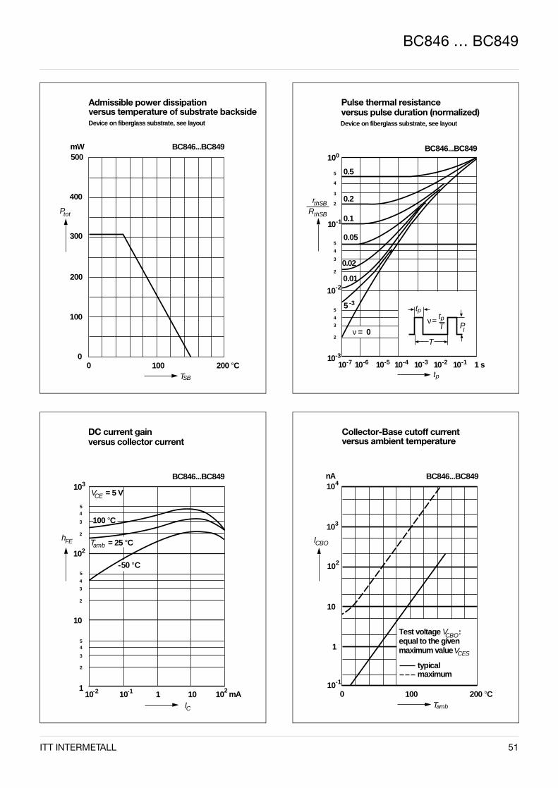
Admissible power dissipationversus temperature of substrate backside
mW500
Ptot
300
200
10000
100
TSB
200 °C
Device on fiberglass substrate, see layout
BC846...BC849
400
Pulse thermal resistanceversus pulse duration (normalized)
10
10
RthSB
tp
Device on fiberglass substrate, see layout
0
5
3
-1
5
2
4
2
10-3
10-7 10-6 10-5 10-4 10-3 10-2 1 s
BC846...BC849
tptpT
ν =PI
T
0.1
0.05
0.02
0.01
ν = 0
4
2
4
3
5
3
10-1
5 -3
0.2
0.5
rthSB
10-2
DC current gainversus collector current
10
5
hFE
101
IC
3BC846...BC849
4
3
2
102
5
4
3
2
10
54
3
2
-2 10-1 101 102 mA
-50 °C
VCE = 5 V
100 °C
Tamb = 25 °C
Collector-Base cutoff currentversus ambient temperature
nA
ICBO
10
1000
1
Tamb
200 °C
BC846...BC849
103
104
102
10-1
Test voltage V :equal to the givenmaximum value
typicalmaximum
VCES
CBO
BC846 … BC849
52 ITT INTERMETALL
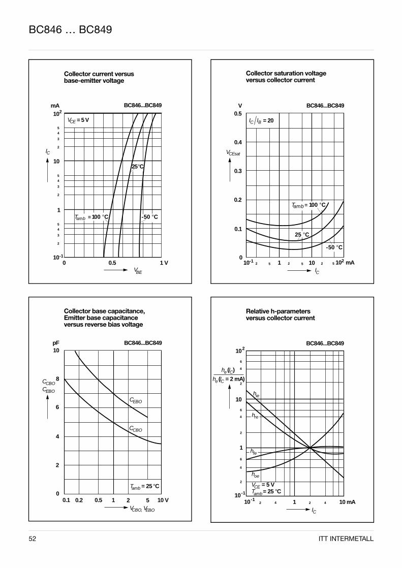
Collector current versusbase-emitter voltage
mA10
5
IC
10
1
010
VBE
BC846...BC8492
4
3
2
5
4
3
2
5
4
3
2
-1
0.5 1 V
Tamb = 100 °C -50 °C
25 °C
VCE = 5 V
Collector saturation voltageversus collector current
V0.5
0.4
VCEsat
0.3
0.2
10
0.1
IC
BC846...BC849
102 5 2 5 2 510-1 10 mA2
-50 °C
25 °C
Tamb= 100 °C
I C = 20I B
BC846 … BC849
Collector base capacitance,Emitter base capacitanceversus reverse bias voltage
pF10
6
4
10.10
2
VCBO,
10 V
BC846...BC849
8
VEBO
0.2 0.5 2 5
CCBOCEBO
CCBO
CEBO
T = 25 °Camb
Relative h-parametersversus collector current
10
110
1
IC
10 mA
BC846...BC849102
6
4
2
6
4
2
6
4
2
-1
10-12 4 2 4
h (I = 2 mA)e C
h (I )e C
hie
hoe
hre
hfe
V = 5 VCET = 25 °Camb
ITT INTERMETALL 53
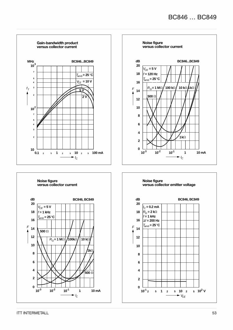
Noise figureversus collector current
dB20
F
12
8
100
6
IC
10 mA
BC846...BC849
18
16
14
10
4
2
-3 10-2 10-1 1
V = 5 VCE
f = 120 Hz
amb
G
500 V
1 kV
T = 25 °C
R = 1 MV 100 kV 10 kV 1 kV
Noise figureversus collector emitter voltage
dB20
F
12
8
100
6
VCE
10 V
BC846, BC849
18
16
14
10
4
2
-12 1 2
I = 0.2 mAC
f = 1 kHz
ambT = 25 °C
R = 2 kVG
Df = 200 Hz
5 5 10 2 52
Noise figureversus collector current
dB20
F
12
8
100
6
IC
10 mA
BC846, BC849
18
16
14
10
4
2
-3 10-2 10-1 1
V = 5 VCE
f = 1 kHz
amb
500 V
1kV
500 V
T = 25 °C
GR = 1 MV 100kV 10 kV
BC846 … BC849
Gain-bandwidth productversus collector current
MHz10
fT
0.1IC
100 mA
BC846...BC8493
7
5
4
3
2
102
7
5
4
3
2
102 5 1 2 5 10 2 5
T = 25 °Camb
V = 10 VCE
5 V
2 V
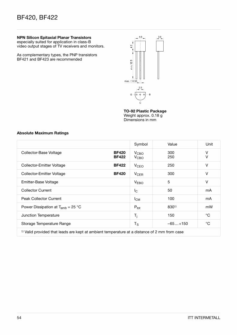
BF420, BF422
NPN Silicon Epitaxial Planar Transistorsespecially suited for application in class-Bvideo output stages of TV receivers and monitors.
As complementary types, the PNP transistorsBF421 and BF423 are recommended
0.55∅ max.
2.5
C
BE
4.6 3.6
TO-92 Plastic PackageWeight approx. 0.18 gDimensions in mm
Absolute Maximum Ratings
Symbol Value Unit
Collector-Base Voltage BF420BF422
VCBOVCBO
300250
VV
Collector-Emitter Voltage BF422 VCEO 250 V
Collector-Emitter Voltage BF420 VCER 300 V
Emitter-Base Voltage VEBO 5 V
Collector Current IC 50 mA
Peak Collector Current ICM 100 mA
Power Dissipation at Tamb = 25 °C Ptot 8301) mW
Junction Temperature Tj 150 °C
Storage Temperature Range TS –65…+150 °C
1) Valid provided that leads are kept at ambient temperature at a distance of 2 mm from case
54 ITT INTERMETALL
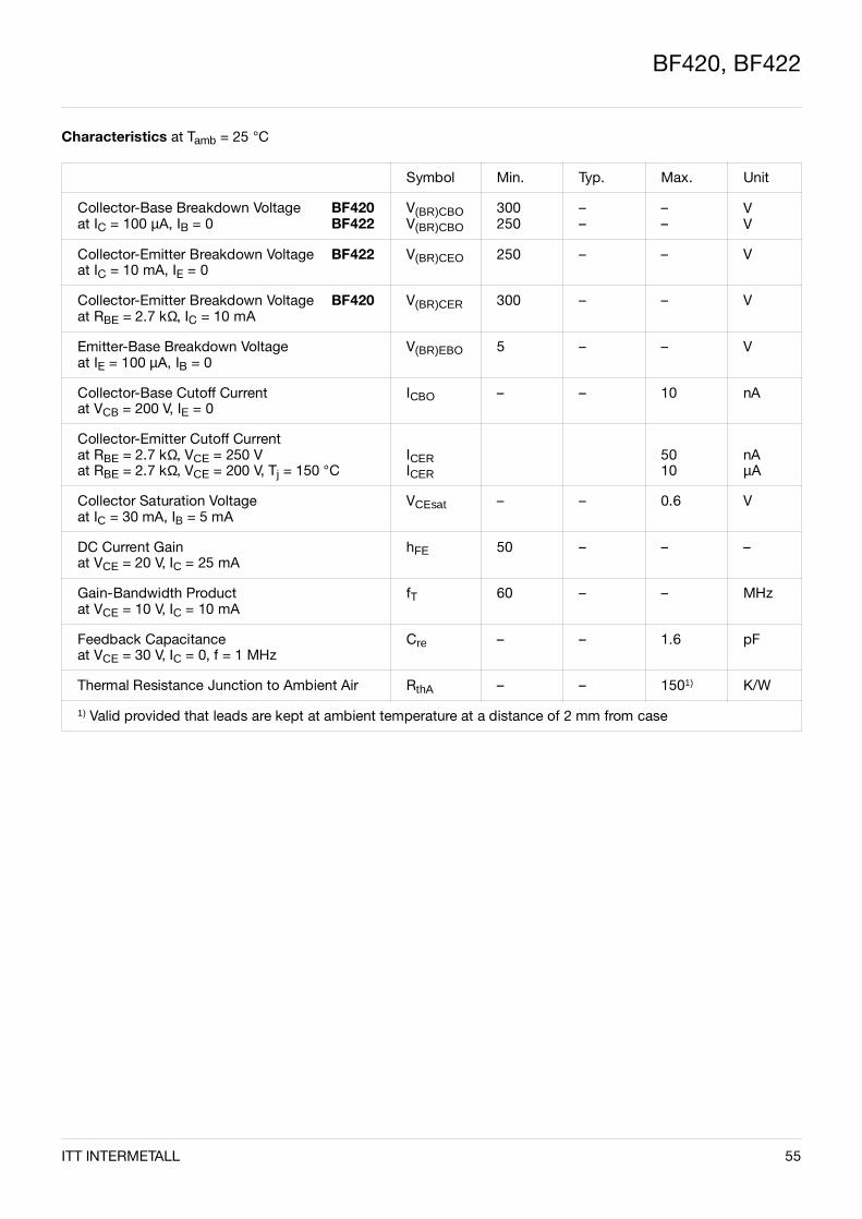
BF420, BF422
Characteristics at Tamb = 25 °C
Symbol Min. Typ. Max. Unit
Collector-Base Breakdown Voltage BF420at IC = 100 µA, IB = 0 BF422
V(BR)CBOV(BR)CBO
300250
––
––
VV
Collector-Emitter Breakdown Voltage BF422at IC = 10 mA, IE = 0
V(BR)CEO 250 – – V
Collector-Emitter Breakdown Voltage BF420at RBE = 2.7 kΩ, IC = 10 mA
V(BR)CER 300 – – V
Emitter-Base Breakdown Voltageat IE = 100 µA, IB = 0
V(BR)EBO 5 – – V
Collector-Base Cutoff Currentat VCB = 200 V, IE = 0
ICBO – – 10 nA
Collector-Emitter Cutoff Currentat RBE = 2.7 kΩ, VCE = 250 Vat RBE = 2.7 kΩ, VCE = 200 V, Tj = 150 °C
ICERICER
5010
nAµA
Collector Saturation Voltageat IC = 30 mA, IB = 5 mA
VCEsat – – 0.6 V
DC Current Gainat VCE = 20 V, IC = 25 mA
hFE 50 – – –
Gain-Bandwidth Productat VCE = 10 V, IC = 10 mA
fT 60 – – MHz
Feedback Capacitanceat VCE = 30 V, IC = 0, f = 1 MHz
Cre – – 1.6 pF
Thermal Resistance Junction to Ambient Air RthA – – 1501) K/W
1) Valid provided that leads are kept at ambient temperature at a distance of 2 mm from case
ITT INTERMETALL 55
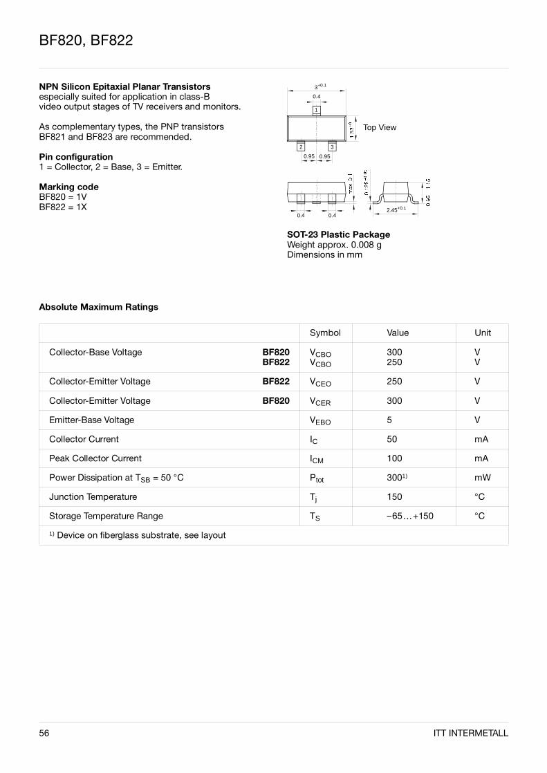
BF820, BF822
NPN Silicon Epitaxial Planar Transistorsespecially suited for application in class-Bvideo output stages of TV receivers and monitors.
As complementary types, the PNP transistors BF821 and BF823 are recommended.
Pin configuration1 = Collector, 2 = Base, 3 = Emitter.
Marking codeBF820 = 1VBF822 = 1X
0.4
0.95 0.95
3
0.4 0.4
+0.1
1
2 3
Top View
SOT-23 Plastic PackageWeight approx. 0.008 gDimensions in mm
2.45+0.1
Absolute Maximum Ratings
Symbol Value Unit
Collector-Base Voltage BF820BF822
VCBOVCBO
300250
VV
Collector-Emitter Voltage BF822 VCEO 250 V
Collector-Emitter Voltage BF820 VCER 300 V
Emitter-Base Voltage VEBO 5 V
Collector Current IC 50 mA
Peak Collector Current ICM 100 mA
Power Dissipation at TSB = 50 °C Ptot 3001) mW
Junction Temperature Tj 150 °C
Storage Temperature Range TS –65…+150 °C
1) Device on fiberglass substrate, see layout
56 ITT INTERMETALL

BF820, BF822
Characteristics at Tamb = 25 °C
Symbol Min. Typ. Max. Unit
Collector-Base Breakdown Voltage BF820at IC = 100 µA, IB = 0 BF822
V(BR)CBOV(BR)CBO
300250
––
––
VV
Collector-Emitter Breakdown Voltage BF822at IC = 10 mA, IE = 0
V(BR)CEO 250 – – V
Collector-Emitter Breakdown Voltage BF820at RBE = 2.7 kΩ, IC = 10 mA
V(BR)CER 300 – – V
Emitter-Base Breakdown Voltageat IE = 100 µA, IB = 0
V(BR)EBO 5 – – V
Collector-Base Cutoff Currentat VCB = 200 V, IE = 0
ICBO – – 10 nA
Collector-Emitter Cutoff Currentat RBE = 2.7 kΩ, VCE = 250 Vat RBE = 2.7 kΩ, VCE = 200 V, Tj = 150 °C
ICERICER
5010
nAµA
Collector Saturation Voltageat IC = 30 mA, IB = 5 mA
VCEsat – – 0.6 V
DC Current Gainat VCE = 20 V, IC = 25 mA
hFE 50 – – –
Gain-Bandwidth Productat VCE = 10 V, IC = 10 mA
fT 60 – – MHz
Feedback Capacitanceat VCE = 30 V, IC = 0, f = 1 MHz
Cre – – 1.6 pF
Thermal Resistance Junction to Ambient Air RthA – – 4301) K/W
1) Device on fiberglass substrate, see layout
Layout for RthA testThickness: Fiberglass 1.5 mm
Copper leads 0.3 mm
15 12
5
0.8
7.5
3
1
1.5
5.1
2
2
1
ITT INTERMETALL 57
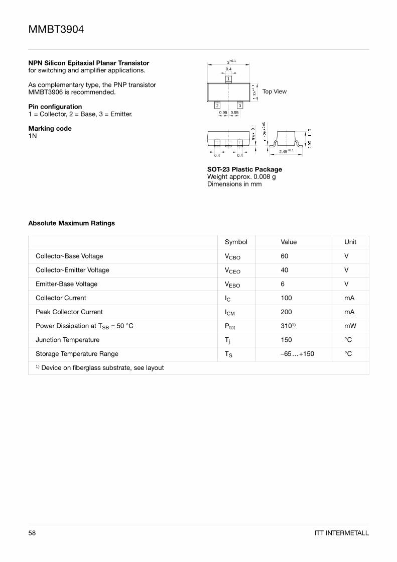
MMBT3904
NPN Silicon Epitaxial Planar Transistorfor switching and amplifier applications.
As complementary type, the PNP transistor MMBT3906 is recommended.
Pin configuration1 = Collector, 2 = Base, 3 = Emitter.
Marking code1N
0.4
0.95 0.95
3
0.4 0.4
+0.1
1
2 3
Top View
SOT-23 Plastic PackageWeight approx. 0.008 gDimensions in mm
2.45+0.1
Absolute Maximum Ratings
Symbol Value Unit
Collector-Base Voltage VCBO 60 V
Collector-Emitter Voltage VCEO 40 V
Emitter-Base Voltage VEBO 6 V
Collector Current IC 100 mA
Peak Collector Current ICM 200 mA
Power Dissipation at TSB = 50 °C Ptot 3101) mW
Junction Temperature Tj 150 °C
Storage Temperature Range TS –65…+150 °C
1) Device on fiberglass substrate, see layout
58 ITT INTERMETALL
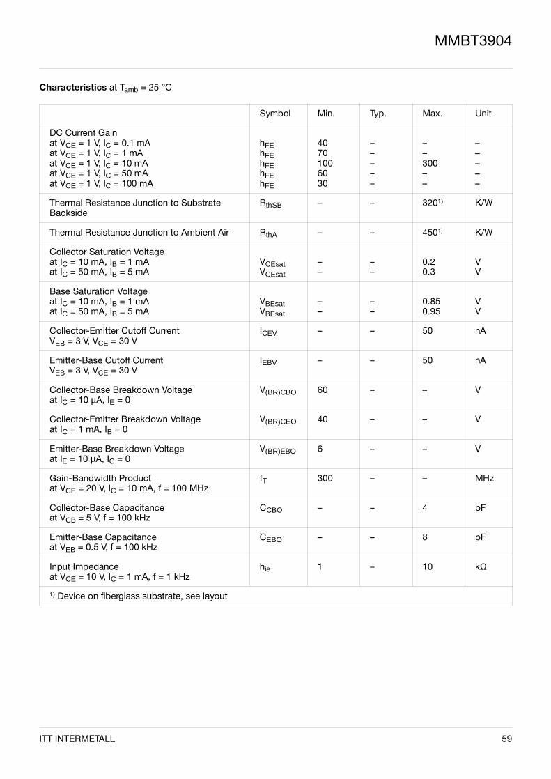
MMBT3904
Characteristics at Tamb = 25 °C
Symbol Min. Typ. Max. Unit
DC Current Gainat VCE = 1 V, IC = 0.1 mAat VCE = 1 V, IC = 1 mAat VCE = 1 V, IC = 10 mAat VCE = 1 V, IC = 50 mAat VCE = 1 V, IC = 100 mA
hFEhFEhFEhFEhFE
40701006030
–––––
––300––
–––––
Thermal Resistance Junction to SubstrateBackside
RthSB – – 3201) K/W
Thermal Resistance Junction to Ambient Air RthA – – 4501) K/W
Collector Saturation Voltageat IC = 10 mA, IB = 1 mAat IC = 50 mA, IB = 5 mA
VCEsatVCEsat
––
––
0.20.3
VV
Base Saturation Voltageat IC = 10 mA, IB = 1 mAat IC = 50 mA, IB = 5 mA
VBEsatVBEsat
––
––
0.850.95
VV
Collector-Emitter Cutoff CurrentVEB = 3 V, VCE = 30 V
ICEV – – 50 nA
Emitter-Base Cutoff CurrentVEB = 3 V, VCE = 30 V
IEBV – – 50 nA
Collector-Base Breakdown Voltageat IC = 10 µA, IE = 0
V(BR)CBO 60 – – V
Collector-Emitter Breakdown Voltageat IC = 1 mA, IB = 0
V(BR)CEO 40 – – V
Emitter-Base Breakdown Voltageat IE = 10 µA, IC = 0
V(BR)EBO 6 – – V
Gain-Bandwidth Productat VCE = 20 V, IC = 10 mA, f = 100 MHz
fT 300 – – MHz
Collector-Base Capacitanceat VCB = 5 V, f = 100 kHz
CCBO – – 4 pF
Emitter-Base Capacitanceat VEB = 0.5 V, f = 100 kHz
CEBO – – 8 pF
Input Impedanceat VCE = 10 V, IC = 1 mA, f = 1 kHz
hie 1 – 10 kΩ
1) Device on fiberglass substrate, see layout
ITT INTERMETALL 59
Characteristics, continuation
MMBT3904
Symbol Min. Typ. Max. Unit
Voltage Feedback Ratioat VCE = 10 V, IC = 1 mA, f = 1 kHz
hre 0.5 · 10–4 – 8 · 10–4 –
Small-Signal Current Gainat VCE = 10 V, IC = 1 mA, f = 1 kHz
hfe 100 – 400 –
Output Admittanceat VCE = 1 V, IC = 1 mA, f = 1 kHz
hoe 1 – 40 µS
Noise Figureat VCE = 5 V, IC = 100 µA, RG = 1 kΩ,f = 10…15000 Hz – – – 5 dB
Delay Time (see Fig. 1)at IB1 = 1 mA, IC = 10 mA
td – – 35 ns
Rise Time (see Fig. 1)at IB1 = 1 mA, IC = 10 mA
tr – – 35 ns
Storage Time (see Fig. 2)at –IB1 = IB2 = 1 mA, IC = 10 mA
ts – – 200 ns
Fall Time (see Fig. 2)at –IB1 = IB2 = 1 mA, IC = 10 mA
tf – – 50 ns
10 < t < 500 msDUTY CYCLE = 2%
0
+ 10.9 V
- 9.1V
+ 3.0 V275
10 K
C < 4.0 pF*3
t11
< 1.0 ns
300 nsDUTY CYCLE = 2%
- 0.5 V
+ 10.9 V
< 1.0 ns
+ 3.0 V275
10 K
C < 4.0 pF*3
Fig. 1: Test circuit for delay and rise time Fig. 2: Test circuit for storage and fall time
* total shunt capacitance of test jig and connectors * total shunt capacitance of test jig and connectors
60 ITT INTERMETALL
Layout for RthA testThickness: Fiberglass 1.5 mm
Copper leads 0.3 mm
15 12
5
0.8
7.5
3
1
1.5
5.1
2
2
1

ITT INTERMETALL 61
MMBT3904
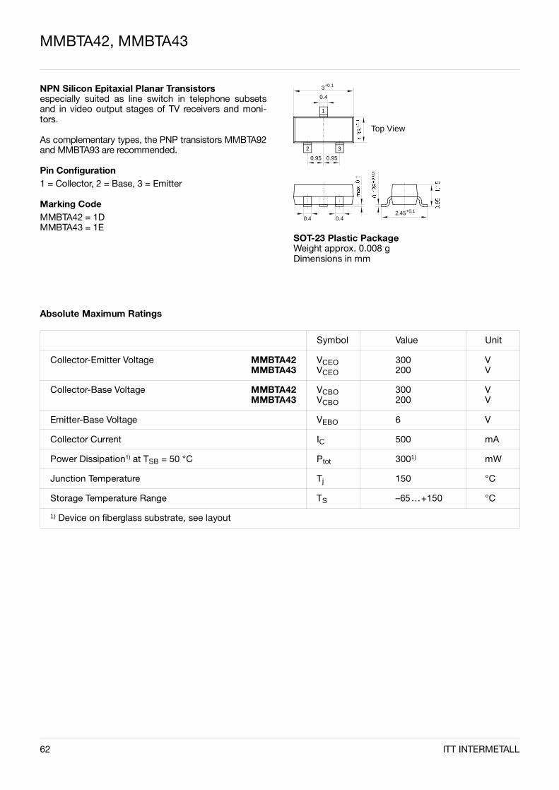
MMBTA42, MMBTA43
NPN Silicon Epitaxial Planar Transistorsespecially suited as line switch in telephone subsetsand in video output stages of TV receivers and moni-tors.
As complementary types, the PNP transistors MMBTA92and MMBTA93 are recommended.
Pin Configuration1 = Collector, 2 = Base, 3 = Emitter
Marking CodeMMBTA42 = 1DMMBTA43 = 1E
0.4
0.95 0.95
3
0.4 0.4
+0.1
1
2 3
Top View
SOT-23 Plastic PackageWeight approx. 0.008 gDimensions in mm
2.45+0.1
Absolute Maximum Ratings
Symbol Value Unit
Collector-Emitter Voltage MMBTA42MMBTA43
VCEOVCEO
300200
VV
Collector-Base Voltage MMBTA42MMBTA43
VCBOVCBO
300200
VV
Emitter-Base Voltage VEBO 6 V
Collector Current IC 500 mA
Power Dissipation1) at TSB = 50 °C Ptot 3001) mW
Junction Temperature Tj 150 °C
Storage Temperature Range TS –65…+150 °C
1) Device on fiberglass substrate, see layout
62 ITT INTERMETALL
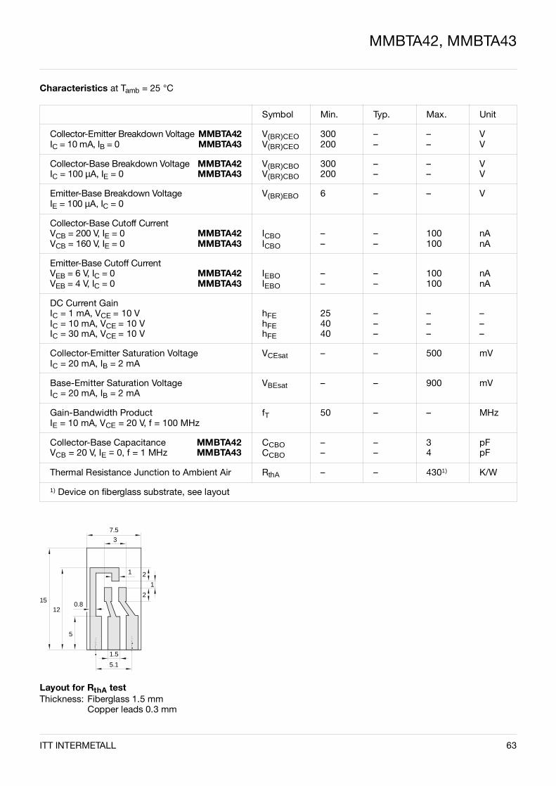
MMBTA42, MMBTA43
Characteristics at Tamb = 25 °C
Symbol Min. Typ. Max. Unit
Collector-Emitter Breakdown Voltage MMBTA42IC = 10 mA, IB = 0 MMBTA43
V(BR)CEOV(BR)CEO
300200
––
––
VV
Collector-Base Breakdown Voltage MMBTA42IC = 100 µA, IE = 0 MMBTA43
V(BR)CBOV(BR)CBO
300200
––
––
VV
Emitter-Base Breakdown VoltageIE = 100 µA, IC = 0
V(BR)EBO 6 – – V
Collector-Base Cutoff CurrentVCB = 200 V, IE = 0 MMBTA42VCB = 160 V, IE = 0 MMBTA43
ICBOICBO
––
––
100100
nAnA
Emitter-Base Cutoff CurrentVEB = 6 V, IC = 0 MMBTA42VEB = 4 V, IC = 0 MMBTA43
IEBOIEBO
––
––
100100
nAnA
DC Current GainIC = 1 mA, VCE = 10 VIC = 10 mA, VCE = 10 VIC = 30 mA, VCE = 10 V
hFEhFEhFE
254040
–––
–––
–––
Collector-Emitter Saturation VoltageIC = 20 mA, IB = 2 mA
VCEsat – – 500 mV
Base-Emitter Saturation VoltageIC = 20 mA, IB = 2 mA
VBEsat – – 900 mV
Gain-Bandwidth ProductIE = 10 mA, VCE = 20 V, f = 100 MHz
fT 50 – – MHz
Collector-Base Capacitance MMBTA42VCB = 20 V, IE = 0, f = 1 MHz MMBTA43
CCBOCCBO
––
––
34
pFpF
Thermal Resistance Junction to Ambient Air RthA – – 4301) K/W
1) Device on fiberglass substrate, see layout
Layout for RthA testThickness: Fiberglass 1.5 mm
Copper leads 0.3 mm
15 12
5
0.8
7.5
3
1
1.5
5.1
2
2
1
ITT INTERMETALL 63
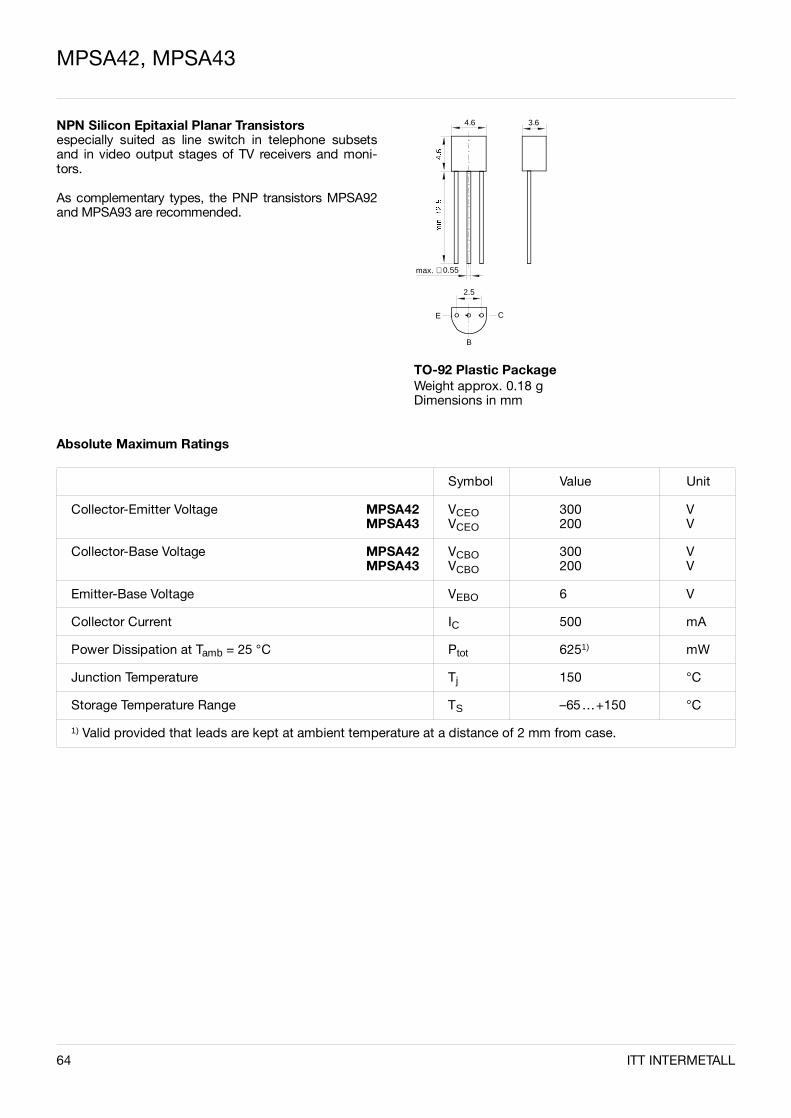
MPSA42, MPSA43
NPN Silicon Epitaxial Planar Transistorsespecially suited as line switch in telephone subsetsand in video output stages of TV receivers and moni-tors.
As complementary types, the PNP transistors MPSA92and MPSA93 are recommended.
0.55∅ max.
2.5
B
CE
4.6 3.6
TO-92 Plastic PackageWeight approx. 0.18 gDimensions in mm
Absolute Maximum Ratings
Symbol Value Unit
Collector-Emitter Voltage MPSA42MPSA43
VCEOVCEO
300200
VV
Collector-Base Voltage MPSA42MPSA43
VCBOVCBO
300200
VV
Emitter-Base Voltage VEBO 6 V
Collector Current IC 500 mA
Power Dissipation at Tamb = 25 °C Ptot 6251) mW
Junction Temperature Tj 150 °C
Storage Temperature Range TS –65…+150 °C
1) Valid provided that leads are kept at ambient temperature at a distance of 2 mm from case.
64 ITT INTERMETALL
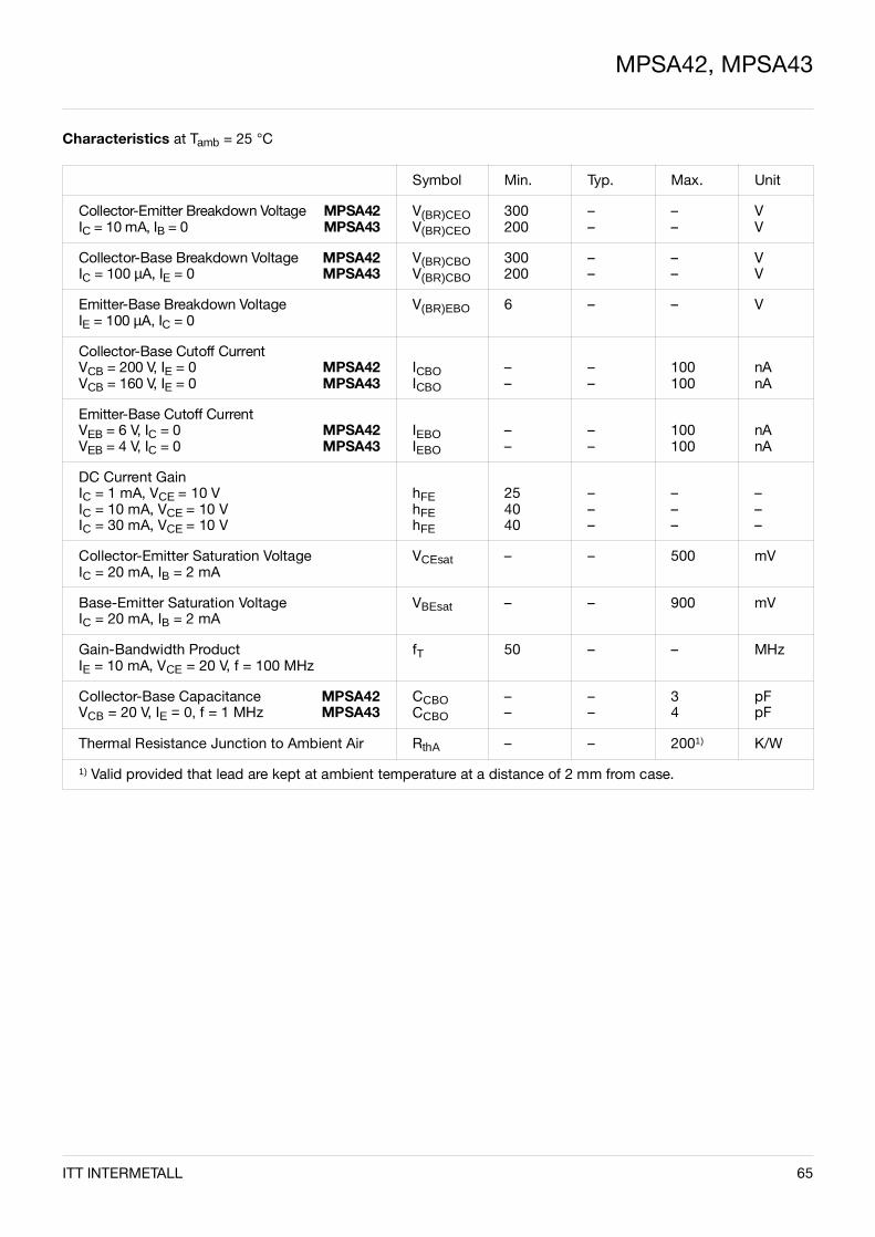
MPSA42, MPSA43
Characteristics at Tamb = 25 °C
Symbol Min. Typ. Max. Unit
Collector-Emitter Breakdown Voltage MPSA42IC = 10 mA, IB = 0 MPSA43
V(BR)CEOV(BR)CEO
300200
––
––
VV
Collector-Base Breakdown Voltage MPSA42IC = 100 µA, IE = 0 MPSA43
V(BR)CBOV(BR)CBO
300200
––
––
VV
Emitter-Base Breakdown VoltageIE = 100 µA, IC = 0
V(BR)EBO 6 – – V
Collector-Base Cutoff CurrentVCB = 200 V, IE = 0 MPSA42VCB = 160 V, IE = 0 MPSA43
ICBOICBO
––
––
100100
nAnA
Emitter-Base Cutoff CurrentVEB = 6 V, IC = 0 MPSA42VEB = 4 V, IC = 0 MPSA43
IEBOIEBO
––
––
100100
nAnA
DC Current GainIC = 1 mA, VCE = 10 VIC = 10 mA, VCE = 10 VIC = 30 mA, VCE = 10 V
hFEhFEhFE
254040
–––
–––
–––
Collector-Emitter Saturation VoltageIC = 20 mA, IB = 2 mA
VCEsat – – 500 mV
Base-Emitter Saturation VoltageIC = 20 mA, IB = 2 mA
VBEsat – – 900 mV
Gain-Bandwidth ProductIE = 10 mA, VCE = 20 V, f = 100 MHz
fT 50 – – MHz
Collector-Base Capacitance MPSA42VCB = 20 V, IE = 0, f = 1 MHz MPSA43
CCBOCCBO
––
––
34
pFpF
Thermal Resistance Junction to Ambient Air RthA – – 2001) K/W
1) Valid provided that lead are kept at ambient temperature at a distance of 2 mm from case.
ITT INTERMETALL 65

66 ITT INTERMETALL
ITT INTERMETALL 67
Small-Signal Transistors (PNP)
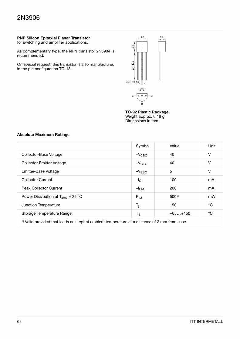
2N3906
PNP Silicon Epitaxial Planar Transistorfor switching and amplifier applications.
As complementary type, the NPN transistor 2N3904 isrecommended.
On special request, this transistor is also manufacturedin the pin configuration TO-18.
0.55∅ max.
2.5
B
CE
4.6 3.6
TO-92 Plastic PackageWeight approx. 0.18 gDimensions in mm
Absolute Maximum Ratings
Symbol Value Unit
Collector-Base Voltage –VCBO 40 V
Collector-Emitter Voltage –VCEO 40 V
Emitter-Base Voltage –VEBO 5 V
Collector Current –IC 100 mA
Peak Collector Current –ICM 200 mA
Power Dissipation at Tamb = 25 °C Ptot 5001) mW
Junction Temperature Tj 150 °C
Storage Temperature Range TS –65…+150 °C
1) Valid provided that leads are kept at ambient temperature at a distance of 2 mm from case.
68 ITT INTERMETALL

2N3906
Characteristics at Tamb = 25 °C
Symbol Min. Typ. Max. Unit
DC Current Gainat –VCE = 1 V, –IC = 0.1 mAat –VCE = 1 V, –IC = 1 mAat –VCE = 1 V, –IC = 10 mAat –VCE = 1 V, –IC = 50 mAat –VCE = 1 V, –IC = 100 mA
hFEhFEhFEhFEhFE
60801006030
–––––
––300––
–––––
Thermal Resistance Junction to Ambient Air RthA – – 2501) K/W
Collector Saturation Voltageat –IC = 10 mA, –IB = 1 mAat –IC = 50 mA, –IB = 5 mA
–VCEsat–VCEsat
––
––
0.250.4
VV
Base Saturation Voltageat –IC = 10 mA, –IB = 1 mAat –IC = 50 mA, –IB = 5 mA
–VBEsat–VBEsat
––
––
0.850.95
VV
Collector-Emitter Cutoff Currentat –VEB = 3 V, –VCE = 30 V
–ICEV – – 50 nA
Emitter-Base Cutoff Currentat –VEB = 3 V, –VCE = 30 V
–IEBV – – 50 nA
Collector-Base Breakdown Voltageat –IC = 10 µA, IE = 0
–V(BR)CBO 40 – – V
Collector-Emitter Breakdown Voltageat –IC = 1 mA, IB = 0
–V(BR)CEO 40 – – V
Emitter-Base Breakdown Voltageat –IE = 10 µA, IC = 0
–V(BR)EBO 5 – – V
Gain-Bandwidth Product at –VCE = 20 V, –IC = 10 mA, f = 100 MHz
fT 250 – – MHz
Collector-Base Capacitanceat –VCB = 5 V, f = 100 kHz
CCBO – – 4.5 pF
Emitter-Base Capacitanceat –VEB = 0.5 V, f = 100 kHz
CEBO – – 10 pF
Input Impedanceat –VCE = 10 V, –IC = 1 mA, f = 1 kHz
hie 1 – 10 kΩ
Voltage Feedback Ratioat –VCE = 10 V, –IC = 1 mA, f = 1 kHz
hre 0.5 · 10–4 – 8 · 10–4 –
1) Valid provided that leads are kept at ambient temperature at a distance of 2 mm from case.
ITT INTERMETALL 69
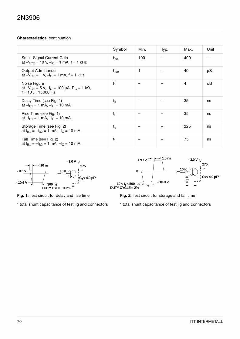
2N3906
Characteristics, continuation
Fig. 1: Test circuit for delay and rise time Fig. 2: Test circuit for storage and fall time
* total shunt capacitance of test jig and connectors * total shunt capacitance of test jig and connectors
Symbol Min. Typ. Max. Unit
Small-Signal Current Gainat –VCE = 10 V, –IC = 1 mA, f = 1 kHz
hfe 100 – 400 –
Output Admittanceat –VCE = 1 V, –IC = 1 mA, f = 1 kHz
hoe 1 – 40 µS
Noise Figureat –VCE = 5 V, –IC = 100 µA, RG = 1 kΩ,f = 10 … 15000 Hz
F – – 4 dB
Delay Time (see Fig. 1)at –IB1 = 1 mA, –IC = 10 mA
td – – 35 ns
Rise Time (see Fig. 1)at –IB1 = 1 mA, –IC = 10 mA
tr – – 35 ns
Storage Time (see Fig. 2)at IB1 = –IB2 = 1 mA, –IC = 10 mA
ts – – 225 ns
Fall Time (see Fig. 2)at IB1 = –IB2 = 1 mA, –IC = 10 mA
tf – – 75 ns
300 nsDUTY CYCLE = 2%
- 0.5 V
- 10.6 V
< 10 ns- 3.0 V
27510 K
C < 4.0 pF*3
0
+ 9.1V - 3.0 V275
10 K
C < 4.0 pF*3
10 < t < 500 msDUTY CYCLE = 2%
- 10.9 Vt11
< 1.0 ns
70 ITT INTERMETALL

ITT INTERMETALL 71
2N3906
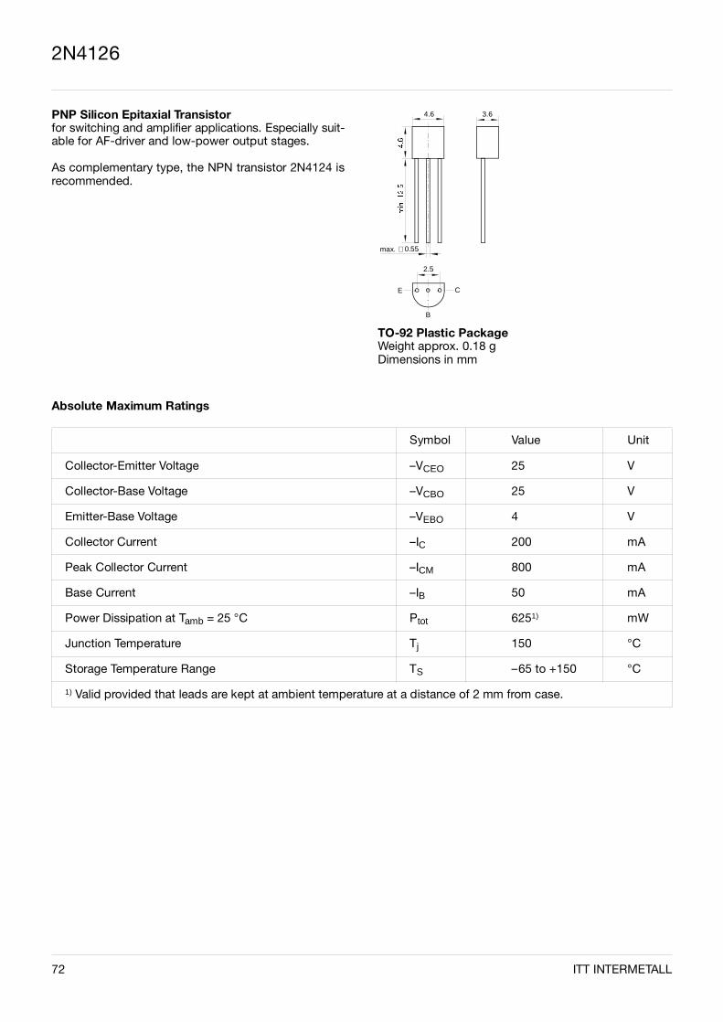
2N4126
Absolute Maximum Ratings
Symbol Value Unit
Collector-Emitter Voltage –VCEO 25 V
Collector-Base Voltage –VCBO 25 V
Emitter-Base Voltage –VEBO 4 V
Collector Current –IC 200 mA
Peak Collector Current –ICM 800 mA
Base Current –IB 50 mA
Power Dissipation at Tamb = 25 °C Ptot 6251) mW
Junction Temperature Tj 150 °C
Storage Temperature Range TS –65 to +150 °C
1) Valid provided that leads are kept at ambient temperature at a distance of 2 mm from case.
PNP Silicon Epitaxial Transistorfor switching and amplifier applications. Especially suit-able for AF-driver and low-power output stages.
As complementary type, the NPN transistor 2N4124 isrecommended.
72
0.55∅ max.
2.5
B
CE
4.6 3.6
TO-92 Plastic PackageWeight approx. 0.18 gDimensions in mm
ITT INTERMETALL
2N4126
Characteristics at Tamb = 25 °C
Symbol Min. Typ. Max. Unit
DC Current Gainat VCE = –1 V, IC = –2.0 mAat VCE = –1 V, IC = –50 mA
hFEhFE
120–
–60
360–
––
Collector Cutoff Currentat VCB = –20 V
–ICBO – – 50 nA
Emitter Cutoff Currentat VEB = –3 V
–IEBO – – 50 nA
Collector Saturation Voltageat IC = –50 mA, IB = –5 mA
–VCESAT – – 0.4 V
Base Saturation Voltageat IC = –50 mA, IB = –5 mA
–VBESAT – – 0.95 V
Collector-Emitter Breakdown Voltageat IC = –1 mA
–V(BR)CEO 25 – – V
Collector-Base Breakdown Voltageat IC = –10 µA
–V(BR)CBO 25 – – V
Emitter-Base Breakdown Voltageat IE = –10 µA
–V(BR)EBO 4 – – V
Gain-Bandwidth Productat VCE = –5 V, IC = –10 mA, f = 50 MHz
fT – 200 – MHz
Collector-Base Capacitanceat VCB = –10 V, f = 1 MHz
CCBO – 12 – pF
Thermal Resistance Junction to Ambient Air RthA – – 2001) K/W
1) Valid provided that leads are kept at ambient temperature at a distance of 2 mm from case.
ITT INTERMETALL 73
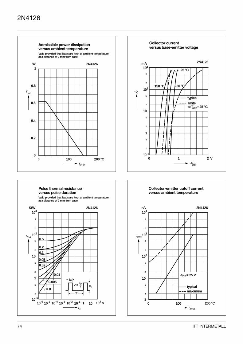
74 ITT INTERMETALL
Collector-emitter cutoff current versus ambient temperature
nA
-ICES
Tamb
2N4126
2
104
5
103
5
2
10
5
2
5
2
10 100 200 °C
10
2
-V = 25 VCE
typicalmaximum
Pulse thermal resistance versus pulse duration
K/W
rthA
1
tp
Valid provided that leads are kept at ambient temperatureat a distance of 2 mm from case
2N4126
2
103
5
102
5
2
10
5
2
5
2
10-1
10-6 10-4 10-2 1 10 s2
0.5
0.2
0.1
0.05
tpν = tp
T PI
T
10-5
ν = 0
0.005
10-3 10-1 10
0.02
0.01
Collector current versus base-emitter voltage
mA10
10-IC
10
1
-VBE
3
5
2
2
5
2
5
2
5
2
10-1
0 1 2 V
2N4126
-50 °C
25 °C
150 °C
typical
at T = 25 °Camb
limits
Admissible power dissipation versus ambient temperature
W1
Ptot
0.6
0.4
10000
0.2
Tamb
200 °C
Valid provided that leads are kept at ambient temperatureat a distance of 2 mm from case
2N4126
0.8
2N4126
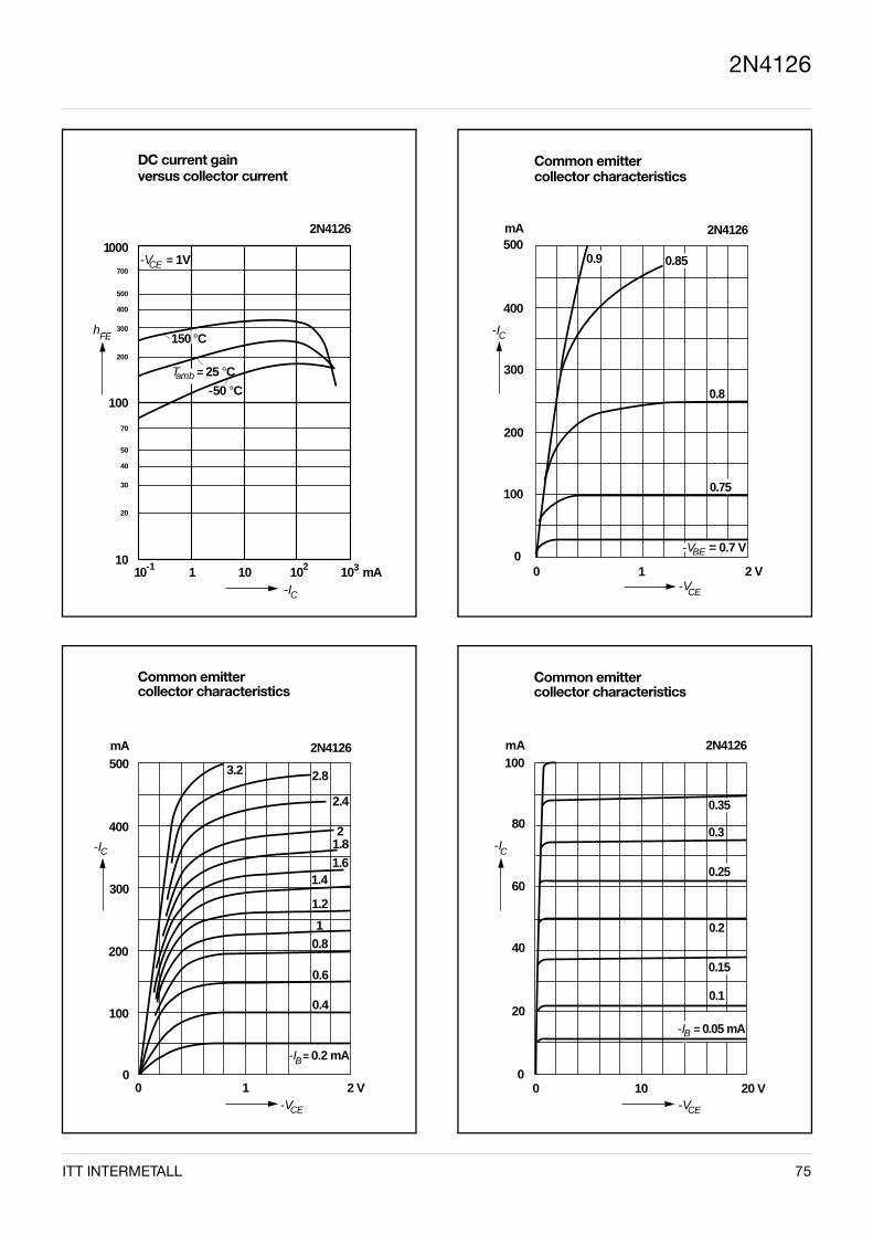
ITT INTERMETALL 75
Common emitter collector characteristics
mA100
-IC
1000
-VCE
20 V
80
60
40
200.1
0.2
0.3
2N4126
-I = 0.05 mAB
0.15
0.25
0.35
Common emitter collector characteristics
500
400
-IC
300
200
100
100
-VCE
2 V
-I = 0.2 mAB
2N4126
0.8
0.6
0.4
1.4
1.2
1
1.6
1.82
2.4
2.83.2
mA
Common emitter collector characteristics
mA500
400
-IC
300
200
100
100
-VCE
2 V
0.8
2N4126
0.75
0.850.9
-V = 0.7 VBE
-1
DC current gain versus collector current
1000
hFE
100
10
-IC
700
500
400
300
200
70
50
40
30
20
10 1 10 102 10 mA3
2N4126
-50 °C
-V = 1VCE
150 °C
T = 25 °Camb
2N4126
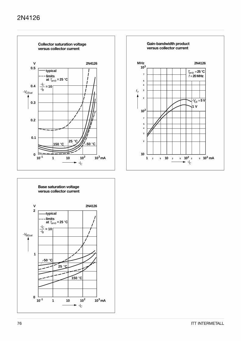
76 ITT INTERMETALL
Base saturation voltage versus collector current
V2
1
10100
-I
2N4126
-V
-I
-1 1 102 310
typical
limitsat
BEsat
= 25 °CTamb
C
-IB= 10
150 °C
25 °C
-50 °C
C
mA
Gain-bandwidth product versus collector current
MHz10
10
-IC
3
7
2
2
101
2N4126
5
4
3
7
2
5
4
3
2 5 10 2 5 1022 5 10 mA3
Tamb = 25 °Cf = 20 MHz
-VCE = 5 V
1 V
fT
Collector saturation voltage versus collector current
V0.5
10100
-I
2N4126
-V
-I
-1 1 102 310
typical
limitsat
CEsat
= 25 °CTamb
C
-IB= 10
150 °C25 °C
-50 °C
C
mA
0.4
0.3
0.2
0.1
2N4126

ITT INTERMETALL 77
2N4126
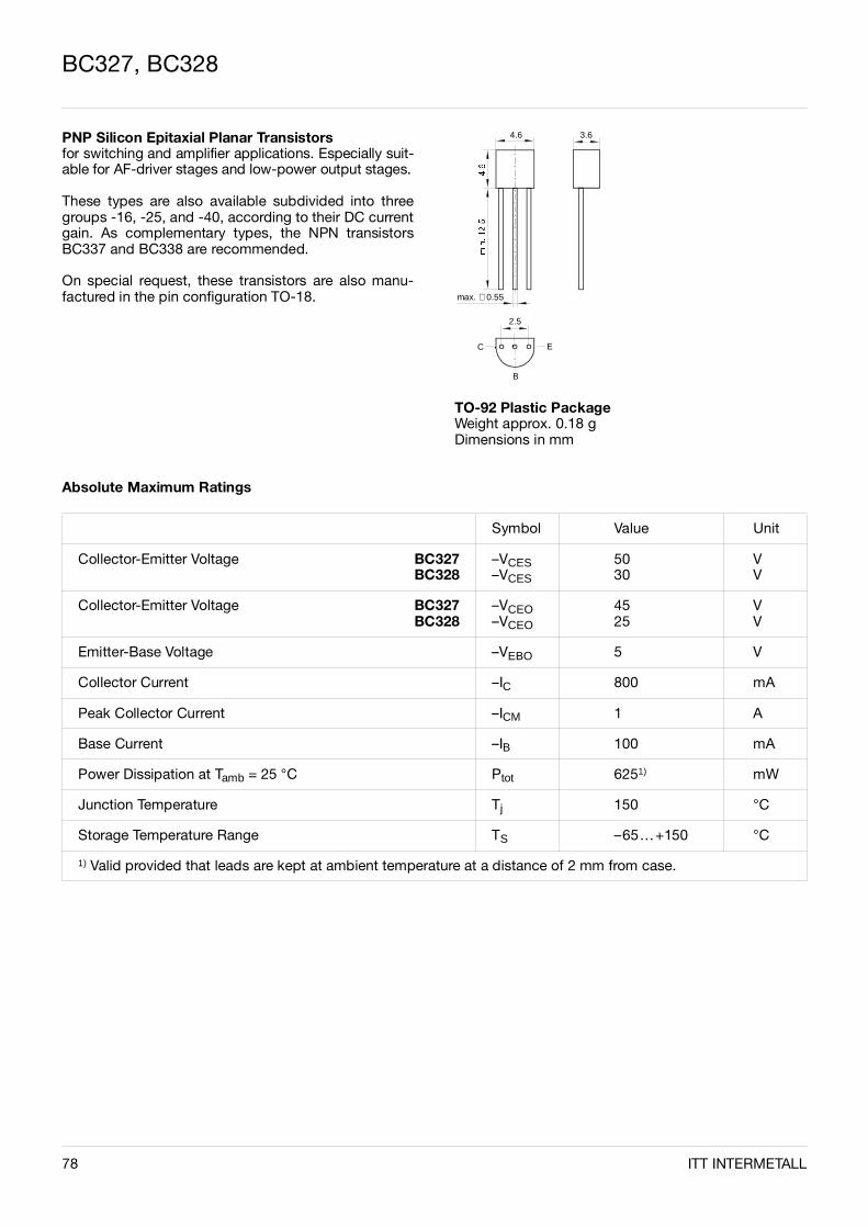
BC327, BC328
PNP Silicon Epitaxial Planar Transistorsfor switching and amplifier applications. Especially suit-able for AF-driver stages and low-power output stages.
These types are also available subdivided into threegroups -16, -25, and -40, according to their DC currentgain. As complementary types, the NPN transistorsBC337 and BC338 are recommended.
On special request, these transistors are also manu-factured in the pin configuration TO-18. 0.55∅ max.
2.5
B
EC
4.6 3.6
TO-92 Plastic PackageWeight approx. 0.18 gDimensions in mm
Absolute Maximum Ratings
Symbol Value Unit
Collector-Emitter Voltage BC327BC328
–VCES–VCES
5030
VV
Collector-Emitter Voltage BC327BC328
–VCEO–VCEO
4525
VV
Emitter-Base Voltage –VEBO 5 V
Collector Current –IC 800 mA
Peak Collector Current –ICM 1 A
Base Current –IB 100 mA
Power Dissipation at Tamb = 25 °C Ptot 6251) mW
Junction Temperature Tj 150 °C
Storage Temperature Range TS –65…+150 °C
1) Valid provided that leads are kept at ambient temperature at a distance of 2 mm from case.
78 ITT INTERMETALL

BC327, BC328
Characteristics at Tamb = 25 °C
Symbol Min. Typ. Max. Unit
DC Current Gainat –VCE = 1 V, –IC = 100 mA
Current Gain Group-16-25-40
at –VCE = 1 V, –IC = 300 mACurrent Gain Group-16
-25-40
hFEhFEhFE
hFEhFEhFE
100160250
60100170
160250400
130200320
250400630
–––
–––
–––
Thermal Resistance Junction to Ambient Air RthA – – 2001) K/W
Collector-Emitter Cutoff Currentat –VCE = 45 V BC327at –VCE = 25 V BC328at –VCE = 45 V, Tamb = 125 °C BC327at –VCE = 25 V, Tamb = 125 °C BC328
–ICES–ICES–ICES–ICES
––––
22––
1001001010
nAnAµAµA
Collector-Emitter Breakdown Voltageat –IC = 10 mA BC327
BC328–V(BR)CEO–V(BR)CEO
4525
––
––
VV
Collector-Emitter Breakdown Voltageat –IC = 0.1 mA BC327
BC328–V(BR)CES–V(BR)CES
5030
––
––
VV
Emitter-Base Breakdown Voltageat –IE = 0.1 mA
–V(BR)EBO 5 – – V
Collector Saturation Voltageat –IC = 500 mA, –IB = 50 mA
–VCEsat – – 0.7 V
Base-Emitter Voltageat –VCE = 1 V, –IC = 300 mA
–VBE – – 1.2 V
Gain-Bandwidth Productat –VCE = 5 V, –IC = 10 mA, f = 50 MHz
fT – 100 – MHz
Collector-Base Capacitanceat –VCB = 10 V, f = 1 MHz
CCBO – 12 – pF
1) Valid provided that leads are kept at ambient temperature at a distance of 2 mm from case.
ITT INTERMETALL 79
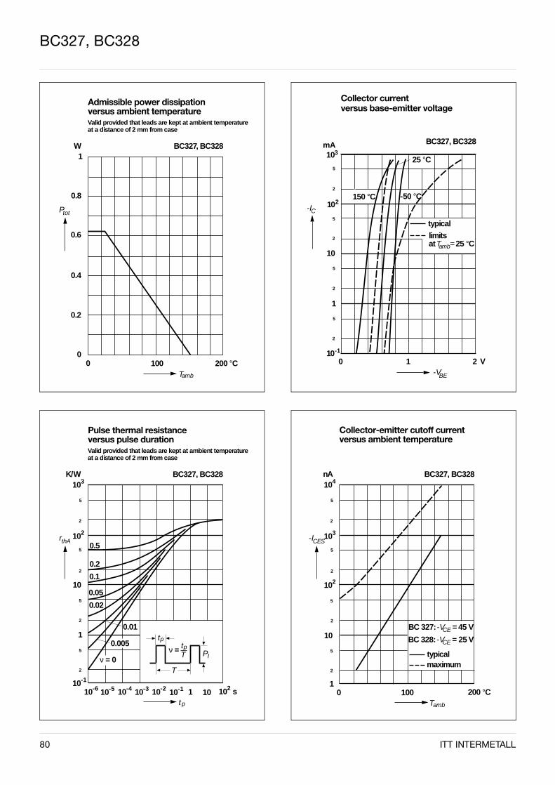
80 ITT INTERMETALL
BC327, BC328
Admissible power dissipation versus ambient temperature
W1
Ptot
0.6
0.4
10000
0.2
Tamb
200 °C
Valid provided that leads are kept at ambient temperatureat a distance of 2 mm from case
BC327, BC328
0.8
Pulse thermal resistance versus pulse duration
K/W
rthA
1
tp
Valid provided that leads are kept at ambient temperatureat a distance of 2 mm from case
BC327, BC328
2
103
5
102
5
2
10
5
2
5
2
10-1
10-6 10-4 10-2 1 10 s2
0.5
0.2
0.1
0.05
tpν = tp
T PI
T
10-5
ν = 0
0.005
10-3 10-1 10
0.02
0.01
Collector current versus base-emitter voltage
mA10
10-IC
10
1
-VBE
3
5
2
2
5
2
5
2
5
2
10-1
0 1 2 V
BC327, BC328
-50 °C
25 °C
150 °C
typical
at T = 25 °Camb
limits
Collector-emitter cutoff current versus ambient temperature
nA
-ICES
Tamb
BC327, BC328
2
104
5
103
5
2
10
5
2
5
2
10 100 200 °C
10
2
BC 327: -V = 45 VCE
BC 328: -V = 25 VCE
typicalmaximum
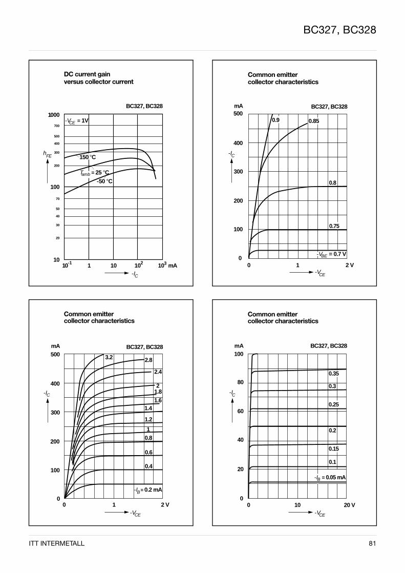
ITT INTERMETALL 81
BC327, BC328
-1
DC current gain versus collector current
1000
hFE
100
10
-IC
700
500
400
300
200
70
50
40
30
20
10 1 10 102 10 mA3
BC327, BC328
-50 °C
-V = 1VCE
150 °C
T = 25 °Camb
Common emitter collector characteristics
500
400
-IC
300
200
100
100
-VCE
2 V
-I = 0.2 mAB
BC327, BC328
0.8
0.6
0.4
1.4
1.2
1
1.6
1.82
2.4
2.83.2
mA
Common emitter collector characteristics
mA500
400
-IC
300
200
100
100
-VCE
2 V
0.8
BC327, BC328
0.75
0.850.9
-V = 0.7 VBE
Common emitter collector characteristics
mA100
-IC
1000
-VCE
20 V
80
60
40
200.1
0.2
0.3
BC327, BC328
-I = 0.05 mAB
0.15
0.25
0.35
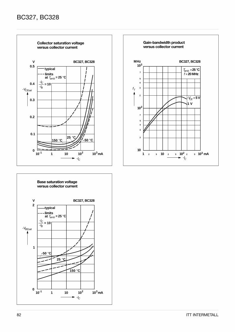
82 ITT INTERMETALL
BC327, BC328
Collector saturation voltage versus collector current
V0.5
10100
-I
BC327, BC328
-V
-I
-1 1 102 310
typical
limitsat
CEsat
= 25 °CTamb
C
-IB= 10
150 °C25 °C
-50 °C
C
mA
0.4
0.3
0.2
0.1
Base saturation voltage versus collector current
V2
1
10100
-I
BC327, BC328
-V
-I
-1 1 102 310
typical
limitsat
BEsat
= 25 °CTamb
C
-IB= 10
150 °C
25 °C
-50 °C
C
mA
Gain-bandwidth product versus collector current
MHz10
10
-IC
3
7
2
2
101
BC327, BC328
5
4
3
7
2
5
4
3
2 5 10 2 5 1022 5 10 mA3
Tamb = 25 °Cf = 20 MHz
-VCE = 5 V
1 V
fT

ITT INTERMETALL 83
BC327, BC328
BC556 … BC559
PNP Silicon Epitaxial Planar Transistorsfor switching and AF amplifier applications.
These transistors are subdivided into three groups A, Band C according to their current gain. The type BC556is available in groups A and B, however, the typesBC557 and BC558 can be supplied in all three groups.The BC559 is a low-noise type available in all threegroups. As complementary types, the NPN transistorsBC546 … BC549 are recommended.
On special request, these transistors are also manu-factured in the pin configuration TO-18.
0.55∅ max.
2.5
B
EC
4.6 3.6
TO-92 Plastic PackageWeight approx. 0.18 gDimensions in mm
Absolute Maximum Ratings
Symbol Value Unit
Collector-Base Voltage BC556BC557
BC558, BC559
–VCBO–VCBO–VCBO
805030
VVV
Collector-Emitter Voltage BC556BC557
BC558, BC559
–VCES–VCES–VCES
805030
VVV
Collector-Emitter Voltage BC556BC557
BC558, BC559
–VCEO–VCEO–VCEO
654530
VVV
Emitter-Base Voltage –VEBO 5 V
Collector Current –IC 100 mA
Peak Collector Current –ICM 200 mA
Peak Base Current –IBM 200 mA
Peak Emitter Current IEM 200 mA
Power Dissipation at Tamb = 25 °C Ptot 5001) mW
Junction Temperature Tj 150 °C
Storage Temperature Range TS –65…+150 °C
1) Valid provided that leads are kept at ambient temperature at a distance of 2 mm from case.
84 ITT INTERMETALL
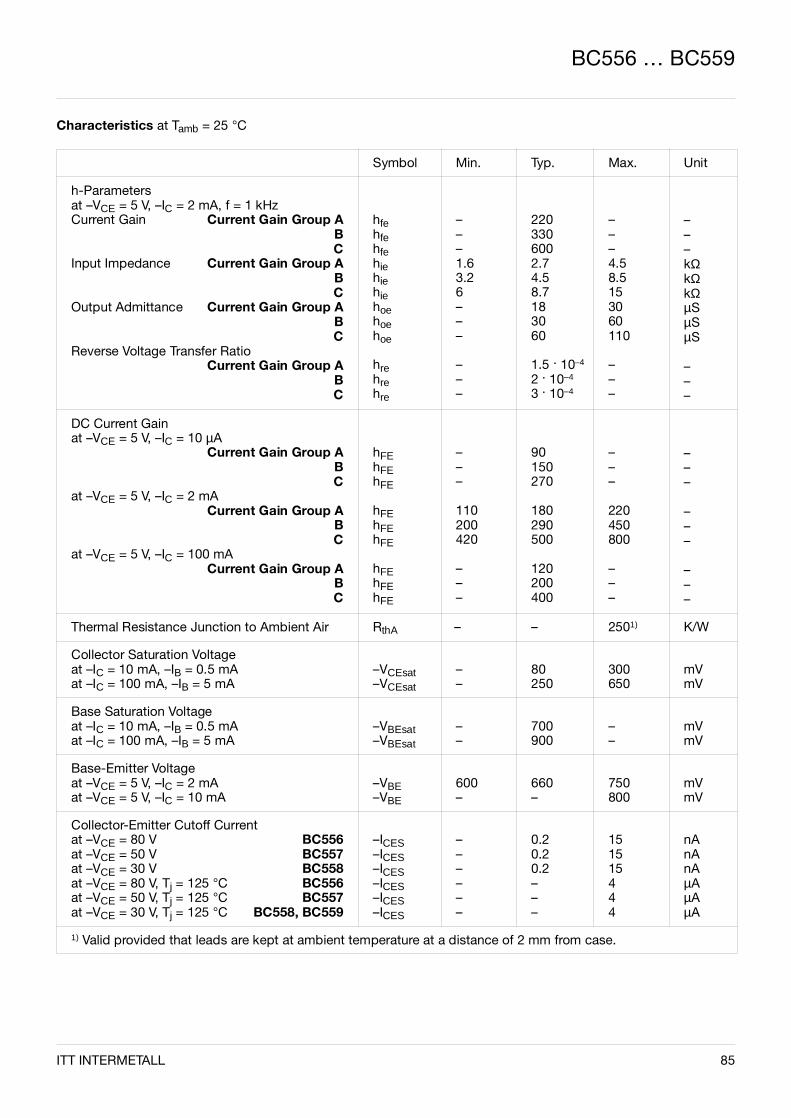
BC556 … BC559
Characteristics at Tamb = 25 °C
Symbol Min. Typ. Max. Unit
h-Parametersat –VCE = 5 V, –IC = 2 mA, f = 1 kHzCurrent Gain Current Gain Group A
BC
Input Impedance Current Gain Group ABC
Output Admittance Current Gain Group ABC
Reverse Voltage Transfer RatioCurrent Gain Group A
BC
hfehfehfehiehiehiehoehoehoe
hrehrehre
–––1.63.26–––
–––
2203306002.74.58.7183060
1.5 · 10–4
2 · 10–4
3 · 10–4
–––4.58.5153060110
–––
–––kΩkΩkΩµSµSµS
–––
DC Current Gainat –VCE = 5 V, –IC = 10 µA
Current Gain Group ABC
at –VCE = 5 V, –IC = 2 mACurrent Gain Group A
BC
at –VCE = 5 V, –IC = 100 mACurrent Gain Group A
BC
hFEhFEhFE
hFEhFEhFE
hFEhFEhFE
–––
110200420
–––
90150270
180290500
120200400
–––
220450800
–––
–––
–––
–––
Thermal Resistance Junction to Ambient Air RthA – – 2501) K/W
Collector Saturation Voltageat –IC = 10 mA, –IB = 0.5 mAat –IC = 100 mA, –IB = 5 mA
–VCEsat–VCEsat
––
80250
300650
mVmV
Base Saturation Voltageat –IC = 10 mA, –IB = 0.5 mAat –IC = 100 mA, –IB = 5 mA
–VBEsat–VBEsat
––
700900
––
mVmV
Base-Emitter Voltageat –VCE = 5 V, –IC = 2 mAat –VCE = 5 V, –IC = 10 mA
–VBE–VBE
600–
660–
750800
mVmV
Collector-Emitter Cutoff Currentat –VCE = 80 V BC556at –VCE = 50 V BC557at –VCE = 30 V BC558at –VCE = 80 V, Tj = 125 °C BC556at –VCE = 50 V, Tj = 125 °C BC557at –VCE = 30 V, Tj = 125 °C BC558, BC559
–ICES–ICES–ICES–ICES–ICES–ICES
––––––
0.20.20.2–––
151515444
nAnAnAµAµAµA
1) Valid provided that leads are kept at ambient temperature at a distance of 2 mm from case.
ITT INTERMETALL 85
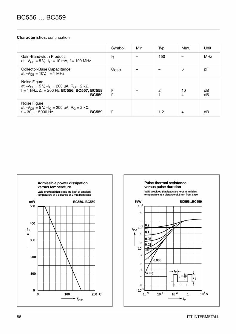
BC556 … BC559
Characteristics, continuation
Symbol Min. Typ. Max. Unit
Gain-Bandwidth Productat –VCE = 5 V, –IC = 10 mA, f = 100 MHz
fT – 150 – MHz
Collector-Base Capacitanceat –VCB = 10V, f = 1 MHz
CCBO – – 6 pF
Noise Figureat –VCE = 5 V, –IC = 200 µA, RG = 2 kΩ,f = 1 kHz, ∆f = 200 Hz BC556, BC557, BC558
BC559FF
––
21
104
dBdB
Noise Figureat –VCE = 5 V, –IC = 200 µA, RG = 2 kΩ,f = 30…15000 Hz BC559 F – 1.2 4 dB
86 ITT INTERMETALL
Pulse thermal resistance versus pulse duration
K/W
rthA
1
tp
Valid provided that leads are kept at ambienttemperature at a distance of 2 mm from case
BC556...BC559
2
103
5
102
5
2
10
5
2
5
2
10-1
10-6 10-4 10-2 1 10 s2
0.2
0.1
0.05
0.02
0.01
0.005
tpν = tp
T PI
T
ν = 0
Admissible power dissipation versus temperature
mW500
Ptot
300
200
10000
100
Tamb
200 °C
Valid provided that leads are kept at ambienttemperature at a distance of 2 mm from case
BC556...BC559
400
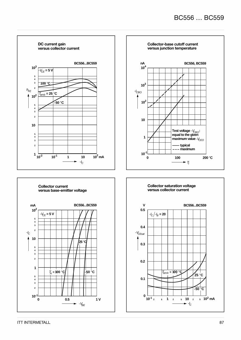
ITT INTERMETALL 87
BC556 … BC559
DC current gain versus collector current
10
5
hFE
101
-IC
3BC556...BC559
4
3
2
102
5
4
3
2
10
54
3
2
-2 10-1 101 102 mA
-50 °C
-VCE = 5 V
100 °C
Tamb = 25 °C
Collector current versus base-emitter voltage
mA10
5
-IC
10
1
010
-VBE
BC556...BC5592
4
3
2
5
4
3
2
5
4
3
2
-1
0.5 1 V
TA = 100 °C -50 °C
25 °C
-VCE = 5 V
Collector-base cutoff current versus junction temperature
nA
-ICBO
10
1000
1
Tj
200 °C
BC556, BC559
103
104
102
10-1
Test voltage -V :equal to the givenmaximum value
typicalmaximum
-VCEO
CBO
Collector saturation voltage versus collector current
V0.5
0.4
-VCEsat
0.3
0.2
10
0.1
-IC
BC556...BC559
102 5 2 5 2 510-1 10 mA2
-50 °C
-I C = 20-I B
Tamb = 100 °C25 °C
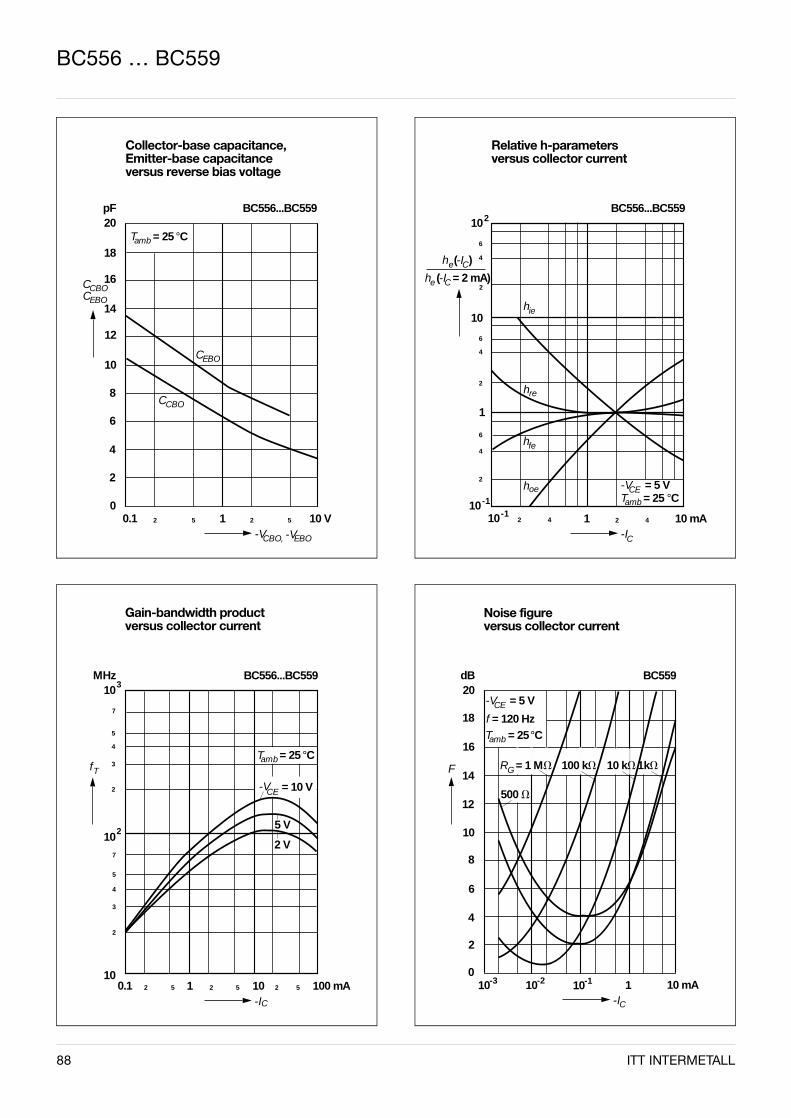
88 ITT INTERMETALL
BC556 … BC559
Collector-base capacitance, Emitter-base capacitance versus reverse bias voltage
pF20
12
8
10.10
4
-VCBO,
10 V
BC556...BC559
16
-VEBO
2
CCBOCEBO
CCBO
CEBO
T = 25 °Camb
18
14
10
6
2
5 2 5
Gain-bandwidth product versus collector current
MHz10
fT
0.1-IC
100 mA
BC556...BC5593
7
5
4
3
2
102
7
5
4
3
2
102 5 1 2 5 10 2 5
5 V
2 V
-V = 10 VCE
T = 25 °Camb
Relative h-parameters versus collector current
10
110
1
-IC
10 mA
BC556...BC559102
6
4
2
6
4
2
6
4
2
-1
10-12 4 2 4
h (-I = 2 mA)e C
h (-I )e C
hie
hoe
hre
hfe
-V = 5 VCET = 25 °Camb
Noise figure versus collector current
dB20
F
12
8
100
6
-IC
10 mA
BC559
18
16
14
10
4
2
-3 10-2 10-1 1
-V = 5 VCE
f = 120 Hz
amb
G
500 V
T = 25 °C
R = 1 MV 100 kV 10 kV 1kV
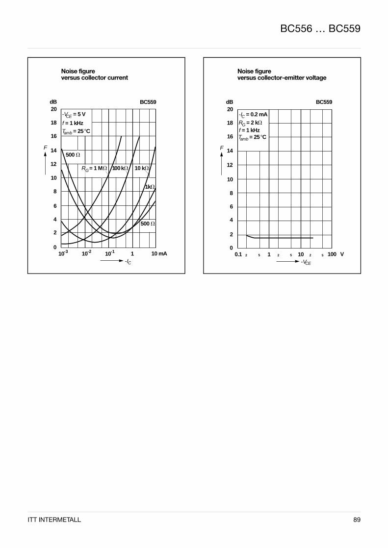
ITT INTERMETALL 89
BC556 … BC559
Noise figure versus collector current
dB20
F
12
8
100
6
-IC
10 mA
BC559
18
16
14
10
4
2
-3 10-2 10-1 1
-V = 5 VCE
f = 1 kHz
amb
500 V
1kV
500 V
T = 25 °C
GR = 1 MV 100 kV 10 kV
Noise figure versus collector-emitter voltage
dB20
F
12
8
0.10
6
-VCE
100 V
BC559
18
16
14
10
4
2
2 1 2
-I = 0.2 mAC
f = 1 kHz
ambT = 25 °C
R = 2 kVG
5 5 10 2 5
BC807, BC808
Absolute Maximum Ratings
Symbol Value Unit
Collector-Emitter Voltage BC807BC808
–VCES–VCES
5030
VV
Collector-Emitter Voltage BC807BC808
–VCEO–VCEO
4525
VV
Emitter-Base Voltage –VEBO 5 V
Collector Current –IC 500 mA
Peak Collector Current –ICM 1000 mA
Peak Base Current –IBM 200 mA
Peak Emitter Current IEM 1000 mA
Power Dissipation at TSB = 50 °C Ptot 3101) mW
Junction Temperature Tj 150 °C
Storage Temperature Range TS –65…+150 °C
1) Device on fiberglass substrate, see layout
PNP Silicon Epitaxial Planar Transistorsfor switching, AF driver and amplifier applications.
Especially suited for automatic insertion in thick- andthin-film circuits.
These transistors are subdivided into three groups -16,-25 and -40 according to their current gain.As complementary types, the NPN transistors BC817and BC818 are recommended.
Pin configuration1 = Collector, 2 = Base, 3 = Emitter.
Marking code
Type Marking
BC807-16-25-40
BC808-16-25-40
5A5B5C
5E5F5G
90
0.4
0.95 0.95
3
0.4 0.4
+0.1
1
2 3
Top View
SOT-23 Plastic PackageWeight approx. 0.008 gDimensions in mm
2.45+0.1
ITT INTERMETALL

BC807, BC808
Characteristics at Tamb = 25 °C
Symbol Min. Typ. Max. Unit
DC Current Gainat –VCE = 1 V, –IC = 100 mA
Current Gain Group-16-25-40
at –VCE = 1 V, –IC = 300 mA -16-25-40
hFEhFEhFEhFEhFEhFE
10016025060100170
––––––
250400600–––
––––––
Thermal Resistance Junction SubstrateBackside
RthSB – – 3201) K/W
Thermal Resistance Junction to Ambient Air RthA – – 4501) K/W
Collector Saturation Voltageat –IC = 500 mA, –IB = 50 mA
–VCEsat – – 0.7 V
Base-Emitter Voltageat –VCE = 1 V, –IC = 300 mA
–VBE – – 1.2 V
Collector-Emitter Cutoff Currentat –VCE = 45 V BC807at –VCE = 25 V BC808at –VCE = 25 V, Tj = 150 °C
–ICES–ICES–ICES
–––
–––
1001005
nAnAµA
Emitter-Base Cutoff Currentat –VEB = 4 V
–IEBO – – 100 nA
Gain-Bandwidth Productat –VCE = 5 V, –IC = 10 mA, f = 50 MHz
fT – 100 – MHz
Collector-Base Capacitanceat –VCB = 10 V, f = 1 MHz
CCBO 12 pF
1) Device on fiberglass substrate, see layout
Layout for RthA testThickness: Fiberglass 1.5 mm
Copper leads 0.3 mm
15 12
5
0.8
7.5
3
1
1.5
5.1
2
2
1
ITT INTERMETALL 91
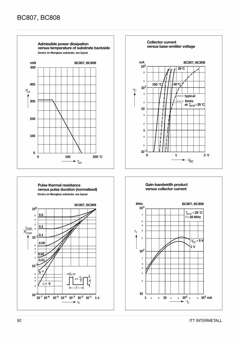
92 ITT INTERMETALL
BC807, BC808
Admissible power dissipation versus temperature of substrate backside
mW500
Ptot
300
200
10000
100
TSR
200 °C
Device on fiberglass substrate, see layout
BC807, BC808
400
Pulse thermal resistance versus pulse duration (normalized)
10
10
RthSB
tp
Device on fiberglass substrate, see layout
0
5
3
-1
5
2
4
2
10-3
10-7 10-6 10-5 10-4 10-3 10-2 1 s
BC807, BC808
tptpT
ν =PI
T
0.1
0.05
0.02
0.01
ν = 0
4
2
4
3
5
3
10-1
5 -3
0.2
0.5
rthSB
10-2
Collector current versus base-emitter voltage
mA10
10-IC
10
1
-VBE
3
5
2
2
5
2
5
2
5
2
10-1
0 1 2 V
BC807, BC808
-50 °C
25 °C
typical
at T =25 °Camblimits
150 °C
Gain-bandwidth product versus collector current
MHz10
10
-IC
3
7
2
2
101
BC807, BC808
5
4
3
7
2
5
4
3
2 5 10 2 5 1022 5 103 mA
Tamb = 25 °Cf = 20 MHz
-VCE = 5 V
1 V
fT
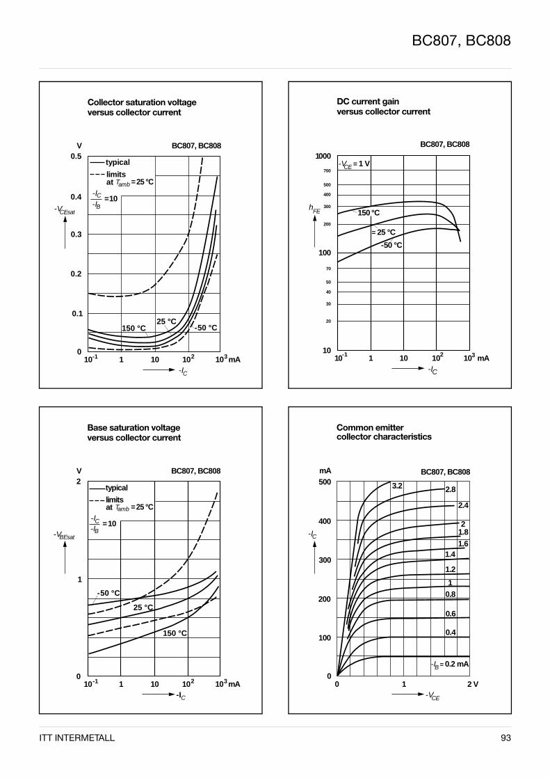
ITT INTERMETALL 93
BC807, BC808
Collector saturation voltage versus collector current
V0.5
10100
-I
BC807, BC808
-V
-I
-1 1 102 310
typical
limitsat
CEsat
= 25 °CTamb
C
-IB= 10
150 °C25 °C
-50 °C
C
mA
0.4
0.3
0.2
0.1
Base saturation voltage versus collector current
V2
1
10100
-I
BC807, BC808
-V
-I
-1 1 102 310
typical
limitsat
BEsat
= 25 °CTamb
C-IB
= 10
150 °C
25 °C
-50 °C
C
mA
-1
DC current gain versus collector current
1000
hFE
100
10
-IC
700
500
400
300
200
70
50
40
30
20
10 1 10 102 10 mA3
BC807, BC808
-50 °C
-V = 1 VCE
150 °C
= 25 °C
Common emitter collector characteristics
500
400
-IC
300
200
100
100
-VCE
2 V
-I = 0.2 mAB
BC807, BC808
0.8
0.6
0.4
1.4
1.2
1
1.6
1.82
2.4
2.83.2
mA
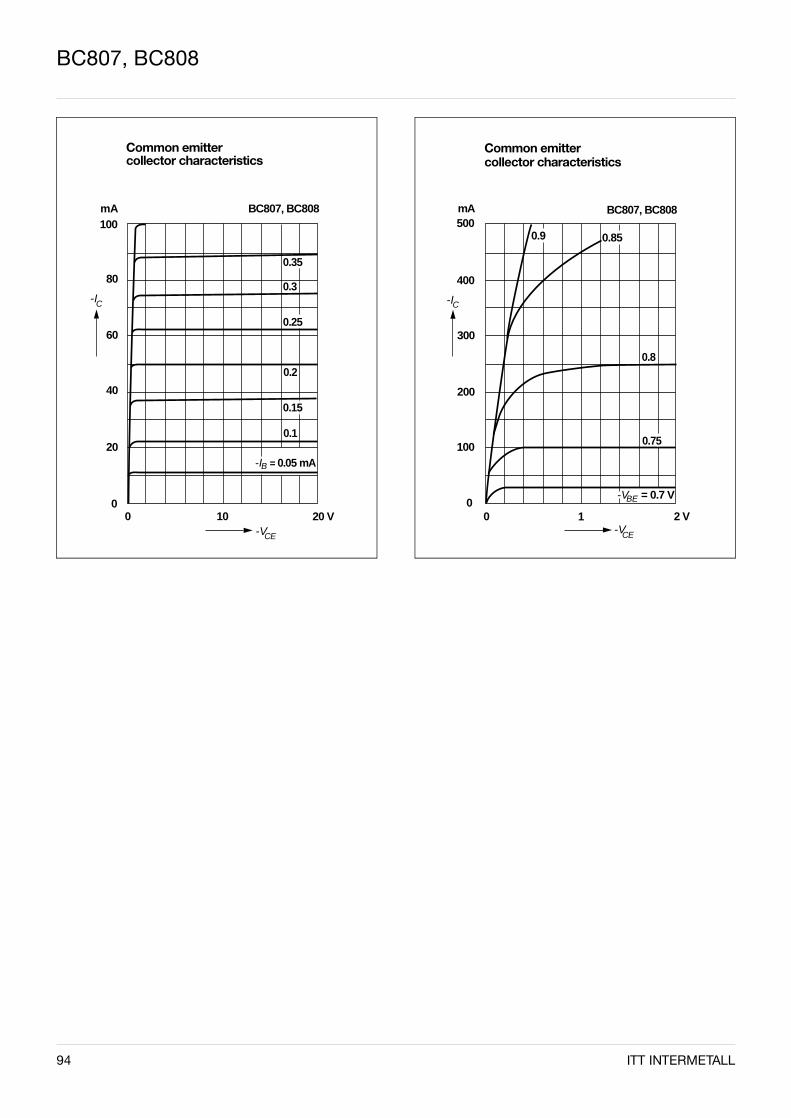
94 ITT INTERMETALL
BC807, BC808
Common emitter collector characteristics
mA100
-IC
1000
-VCE
20 V
80
60
40
200.1
0.2
0.3
BC807, BC808
-I = 0.05 mAB
0.15
0.25
0.35
Common emitter collector characteristics
mA500
400
-IC
300
200
100
100
-VCE
2 V
0.8
BC807, BC808
0.75
0.9
BE-V = 0.7 V
0.85

ITT INTERMETALL 95
BC807, BC808
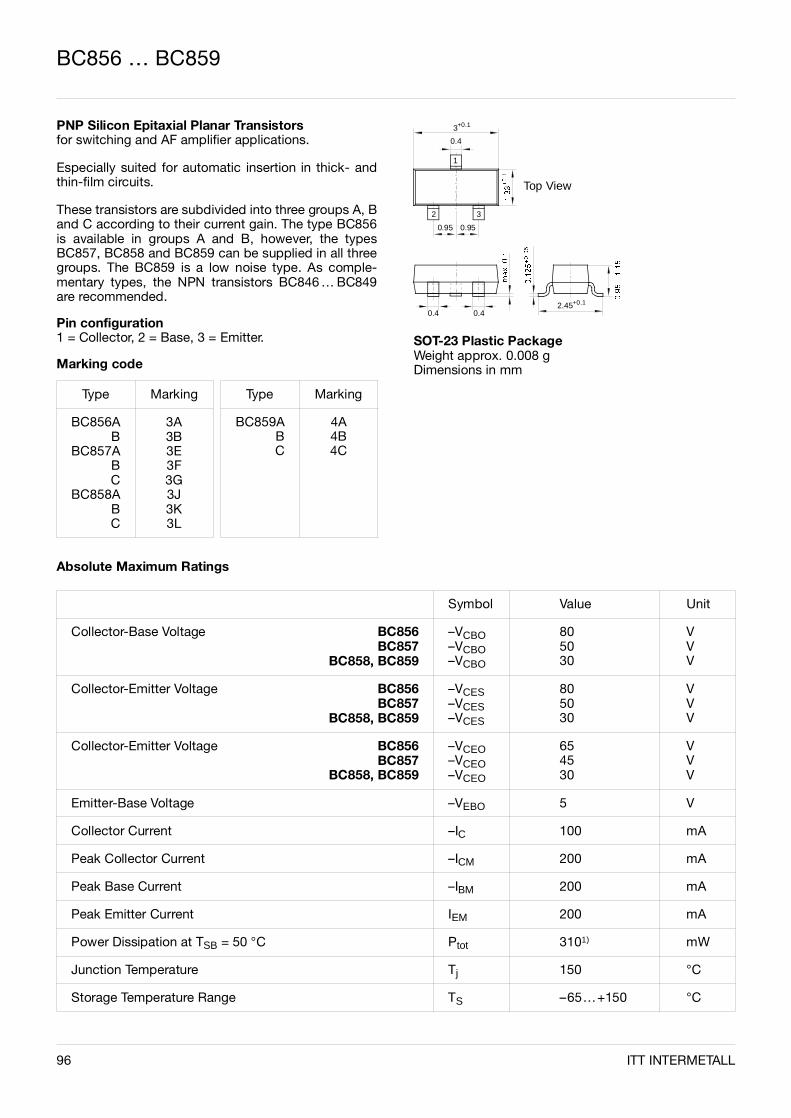
BC856 … BC859
PNP Silicon Epitaxial Planar Transistorsfor switching and AF amplifier applications.
Especially suited for automatic insertion in thick- andthin-film circuits.
These transistors are subdivided into three groups A, Band C according to their current gain. The type BC856is available in groups A and B, however, the typesBC857, BC858 and BC859 can be supplied in all threegroups. The BC859 is a low noise type. As comple-mentary types, the NPN transistors BC846 … BC849are recommended.
Pin configuration1 = Collector, 2 = Base, 3 = Emitter.
Marking code
Type Marking
BC856AB
BC857ABC
BC858ABC
3A3B3E3F3G3J3K3L
Type Marking
BC859ABC
4A4B4C
0.4
0.95 0.95
3
0.4 0.4
+0.1
1
2 3
Top View
SOT-23 Plastic PackageWeight approx. 0.008 gDimensions in mm
2.45+0.1
Absolute Maximum Ratings
Symbol Value Unit
Collector-Base Voltage BC856BC857
BC858, BC859
–VCBO–VCBO–VCBO
805030
VVV
Collector-Emitter Voltage BC856BC857
BC858, BC859
–VCES–VCES–VCES
805030
VVV
Collector-Emitter Voltage BC856BC857
BC858, BC859
–VCEO–VCEO–VCEO
654530
VVV
Emitter-Base Voltage –VEBO 5 V
Collector Current –IC 100 mA
Peak Collector Current –ICM 200 mA
Peak Base Current –IBM 200 mA
Peak Emitter Current IEM 200 mA
Power Dissipation at TSB = 50 °C Ptot 3101) mW
Junction Temperature Tj 150 °C
Storage Temperature Range TS –65…+150 °C
96 ITT INTERMETALL
BC856 … BC859
Characteristics at Tamb = 25 °C
Symbol Min. Typ. Max. Unit
h-Parametersat –VCE = 5 V, –IC = 2 mA, f = 1 kHzCurrent Gain Current Gain Group A
BC
Input Impedance Current Gain Group ABC
Output Admittance Current Gain Group ABC
Reverse Voltage Transfer RatioCurrent Gain Group A
BC
hfehfehfehiehiehiehoehoehoe
hrehrehre
–––1.63.26–––
–––
2203306002.74.58.7183060
1.5 · 10–4
2 · 10–4
3 · 10–4
–––4.58.5153060110
–––
–––kΩkΩkΩµSµSµS
–––
DC Current Gainat –VCE = 5 V, –IC = 10 µA
Current Gain Group ABC
at –VCE = 5 V, –IC = 2 mACurrent Gain Group A
BC
hFEhFEhFE
hFEhFEhFE
–––
110200420
90150270
180290520
–––
220450800
–––
–––
Thermal Resistance Junction to SubstrateBackside
RthSB – – 3201) K/W
Thermal Resistance Junction to Ambient Air RthA – – 4501) K/W
Collector Saturation Voltageat –IC = 10 mA, –IB = 0.5 mAat –IC = 100 mA, –IB = 5 mA
–VCEsat–VCEsat
––
90250
300650
mVmV
Base Saturation Voltageat –IC = 10 mA, –IB = 0.5 mAat –IC = 100 mA, –IB = 5 mA
–VBEsat–VBEsat
––
700900
––
mVmV
Base-Emitter Voltageat –VCE = 5 V, –IC = 2 mAat –VCE = 5 V, –IC = 10 mA
–VBE–VBE
600–
660–
750800
mVmV
Collector-Emitter Cutoff Currentat –VCE = 80 V BC856at –VCE = 50 V BC857at –VCE = 30 V BC858, BC859at –VCE = 80 V, Tj = 125 °C BC856at –VCE = 50 V, Tj = 125 °C BC857at –VCE = 30 V, Tj = 125 °C BC858, BC859at –VCB = 30 Vat –VCB = 30 V, Tj = 150 °C
–ICES–ICES–ICES–ICES–ICES–ICES–ICBO–ICBO
––––––––
0.20.20.2–––––
151515444155
nAnAnAµAµAµAnAµA
Gain-Bandwidth Productat –VCE = 5 V, –IC = 10 mA, f = 100 MHz
fT – 150 – MHz
1) Device on fiberglass substrate, see layout
ITT INTERMETALL 97
BC856 … BC859
Characteristics, continuation
Symbol Min. Typ. Max. Unit
Collector-Base Capacitanceat –VCB = 10 V, f = 1 MHz
CCBO – – 6 pF
Noise Figureat –VCE = 5 V, –IC = 200 µA, RG = 2 kΩ,f = 1 kHz, ∆f = 200 Hz BC856, BC857, BC858
BC859FF
––
21
104
dBdB
Noise Figureat –VCE = 5 V, –IC = 200 µA, RG = 2 kΩ,f = 30…15000 Hz BC859 F – 1.2 4 dB
Layout for RthA testThickness: Fiberglass 1.5 mm
Copper leads 0.3 mm
15 12
5
0.8
7.5
3
1
1.5
5.1
2
2
1
98 ITT INTERMETALL
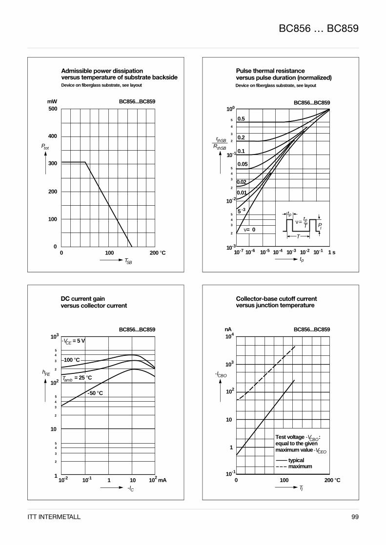
ITT INTERMETALL 99
Admissible power dissipation versus temperature of substrate backside
mW500
Ptot
300
200
10000
100
TSB
200 °C
Device on fiberglass substrate, see layout
BC856...BC859
400
Pulse thermal resistance versus pulse duration (normalized)
10
10
RthSB
tp
Device on fiberglass substrate, see layout
0
5
3
-1
5
2
4
2
10-3
10-7 10-6 10-5 10-4 10-3 10-2 1 s
BC856...BC859
tptpT
ν =PI
T
0.1
0.05
0.02
0.01
ν= 0
4
2
4
3
5
3
10-1
5 -3
0.2
0.5
rthSB
10-2
BC856 … BC859
DC current gain versus collector current
10
5
hFE
101
-IC
3BC856...BC859
4
3
2
102
5
4
3
2
10
54
3
2
-2 10-1 101 102 mA
-50 °C
-VCE = 5 V
100 °C
Tamb = 25 °C
Collector-base cutoff current versus junction temperature
nA
-ICBO
10
1000
1
Tj
200 °C
BC856...BC859
103
104
102
10-1
Test voltage -V :equal to the givenmaximum value
typicalmaximum
-VCEO
CBO
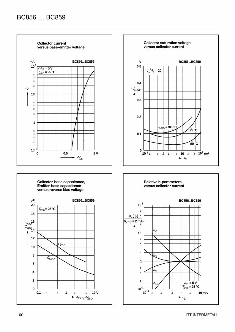
100 ITT INTERMETALL
BC856 … BC859
Collector-base capacitance, Emitter-base capacitance versus reverse bias voltage
pF20
12
8
10.10
4
-VCBO,
10 V
BC856...BC859
16
-VEBO
2
CCBOCEBO
CCBO
CEBO
T = 25 °Camb
18
14
10
6
2
5 2 5
Relative h-parameters versus collector current
10
110
1
-IC
10 mA
BC856...BC859102
6
4
2
6
4
2
6
4
2
-1
10-12 4 2 4
h (-I = 2 mA)e C
h (-I )e C
hie
hoe
hre
hfe
-V = 5 VCET = 25 °Camb
Collector current versus base-emitter voltage
mA10
5
-IC
10
1
010
-VBE
BC856...BC8592
4
3
2
5
4
3
2
5
4
3
2
-1
0.5 1 V
-VCE = 5 VTamb = 25 °C
Collector saturation voltage versus collector current
V0.5
0.4
-VCEsat
0.3
0.2
10
0.1
-IC
BC856...BC859
102 5 2 5 2 510-1 10 mA2
-50 °C
-I C = 20-I B
Tamb = 100 °C25 °C
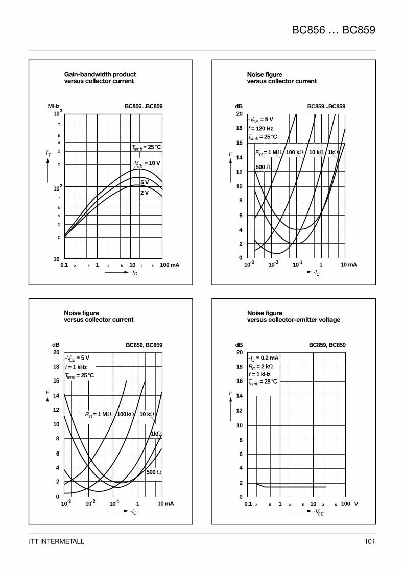
ITT INTERMETALL 101
BC856 … BC859
Noise figure versus collector current
dB20
F
12
8
100
6
-IC
10 mA
BC859, BC859
18
16
14
10
4
2
-3 10-2 10-1 1
-V = 5 VCE
f = 1 kHz
amb
1kV
500 V
T = 25 °C
GR = 1 MV 100 kV 10 kV
Noise figure versus collector-emitter voltage
dB20
F
12
8
0.10
6
-VCE
100 V
BC859, BC859
18
16
14
10
4
2
2 1 2
-I = 0.2 mAC
f = 1 kHz
ambT = 25 °C
R = 2 kVG
5 5 10 2 5
Gain-bandwidth product versus collector current
MHz10
fT
0.1-IC
100 mA
BC856...BC8593
7
5
4
3
2
102
7
5
4
3
2
102 5 1 2 5 10 2 5
5 V
2 V
-V = 10 VCE
T = 25 °Camb
Noise figure versus collector current
dB20
F
12
8
100
6
-IC
10 mA
BC859...BC859
18
16
14
10
4
2
-3 10-2 10-1 1
-V = 5 VCE
f = 120 Hz
amb
G
500 V
T = 25 °C
R = 1 MV 100 kV 10 kV 1kV
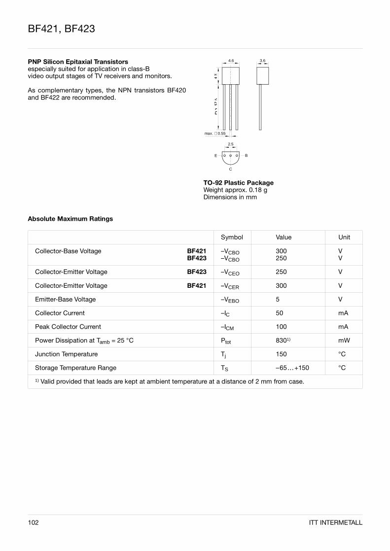
BF421, BF423
PNP Silicon Epitaxial Transistorsespecially suited for application in class-Bvideo output stages of TV receivers and monitors.
As complementary types, the NPN transistors BF420and BF422 are recommended.
0.55∅ max.
2.5
C
BE
4.6 3.6
TO-92 Plastic PackageWeight approx. 0.18 gDimensions in mm
Absolute Maximum Ratings
Symbol Value Unit
Collector-Base Voltage BF421BF423
–VCBO–VCBO
300250
VV
Collector-Emitter Voltage BF423 –VCEO 250 V
Collector-Emitter Voltage BF421 –VCER 300 V
Emitter-Base Voltage –VEBO 5 V
Collector Current –IC 50 mA
Peak Collector Current –ICM 100 mA
Power Dissipation at Tamb = 25 °C Ptot 8301) mW
Junction Temperature Tj 150 °C
Storage Temperature Range TS –65…+150 °C
1) Valid provided that leads are kept at ambient temperature at a distance of 2 mm from case.
102 ITT INTERMETALL
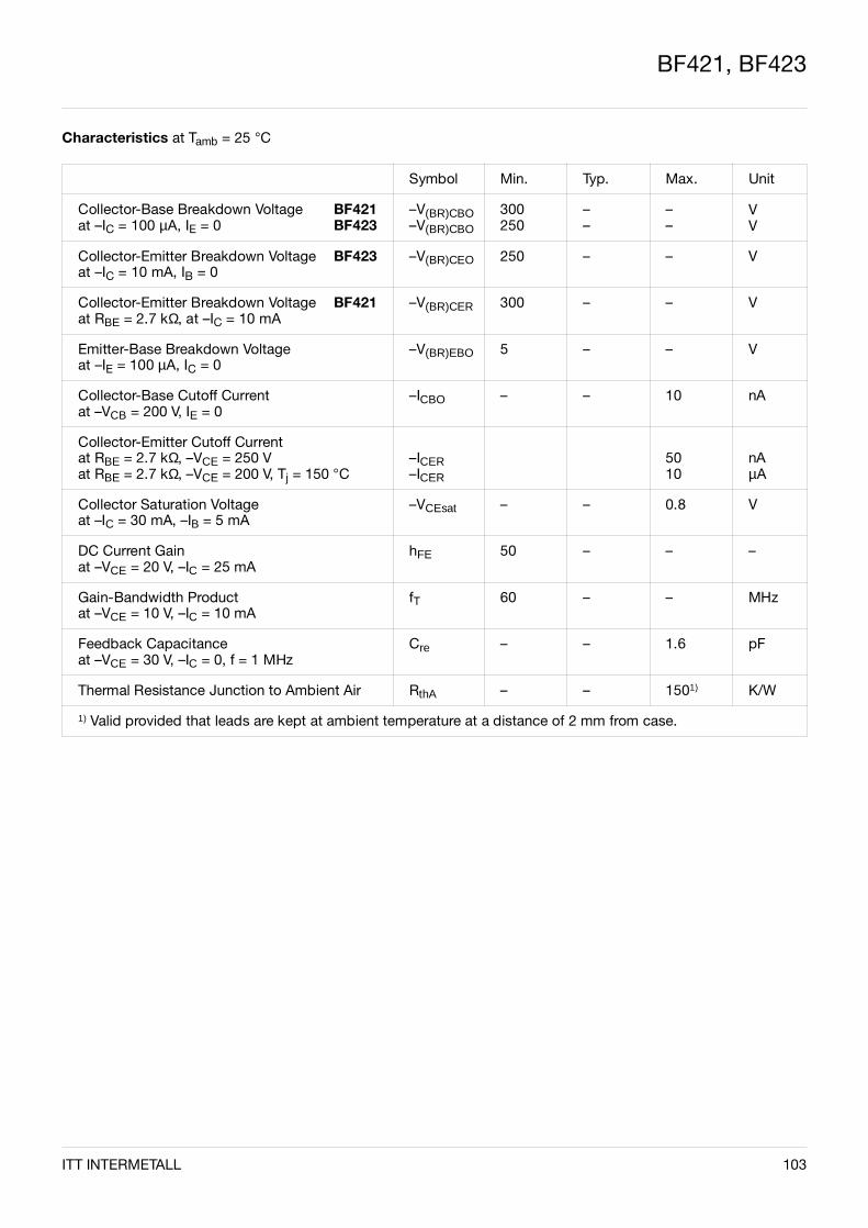
BF421, BF423
Characteristics at Tamb = 25 °C
Symbol Min. Typ. Max. Unit
Collector-Base Breakdown Voltage BF421at –IC = 100 µA, IE = 0 BF423
–V(BR)CBO–V(BR)CBO
300250
––
––
VV
Collector-Emitter Breakdown Voltage BF423at –IC = 10 mA, IB = 0
–V(BR)CEO 250 – – V
Collector-Emitter Breakdown Voltage BF421at RBE = 2.7 kΩ, at –IC = 10 mA
–V(BR)CER 300 – – V
Emitter-Base Breakdown Voltageat –IE = 100 µA, IC = 0
–V(BR)EBO 5 – – V
Collector-Base Cutoff Currentat –VCB = 200 V, IE = 0
–ICBO – – 10 nA
Collector-Emitter Cutoff Currentat RBE = 2.7 kΩ, –VCE = 250 Vat RBE = 2.7 kΩ, –VCE = 200 V, Tj = 150 °C
–ICER–ICER
5010
nAµA
Collector Saturation Voltageat –IC = 30 mA, –IB = 5 mA
–VCEsat – – 0.8 V
DC Current Gainat –VCE = 20 V, –IC = 25 mA
hFE 50 – – –
Gain-Bandwidth Productat –VCE = 10 V, –IC = 10 mA
fT 60 – – MHz
Feedback Capacitanceat –VCE = 30 V, –IC = 0, f = 1 MHz
Cre – – 1.6 pF
Thermal Resistance Junction to Ambient Air RthA – – 1501) K/W
1) Valid provided that leads are kept at ambient temperature at a distance of 2 mm from case.
ITT INTERMETALL 103
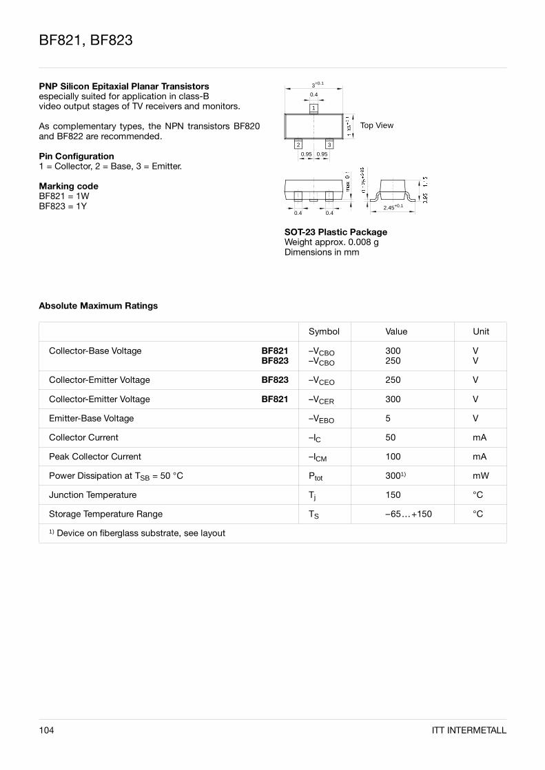
BF821, BF823
PNP Silicon Epitaxial Planar Transistorsespecially suited for application in class-Bvideo output stages of TV receivers and monitors.
As complementary types, the NPN transistors BF820and BF822 are recommended.
Pin Configuration1 = Collector, 2 = Base, 3 = Emitter.
Marking codeBF821 = 1WBF823 = 1Y
0.4
0.95 0.95
3
0.4 0.4
+0.1
1
2 3
Top View
SOT-23 Plastic PackageWeight approx. 0.008 gDimensions in mm
2.45+0.1
Absolute Maximum Ratings
Symbol Value Unit
Collector-Base Voltage BF821BF823
–VCBO–VCBO
300250
VV
Collector-Emitter Voltage BF823 –VCEO 250 V
Collector-Emitter Voltage BF821 –VCER 300 V
Emitter-Base Voltage –VEBO 5 V
Collector Current –IC 50 mA
Peak Collector Current –ICM 100 mA
Power Dissipation at TSB = 50 °C Ptot 3001) mW
Junction Temperature Tj 150 °C
Storage Temperature Range TS –65…+150 °C
1) Device on fiberglass substrate, see layout
104 ITT INTERMETALL
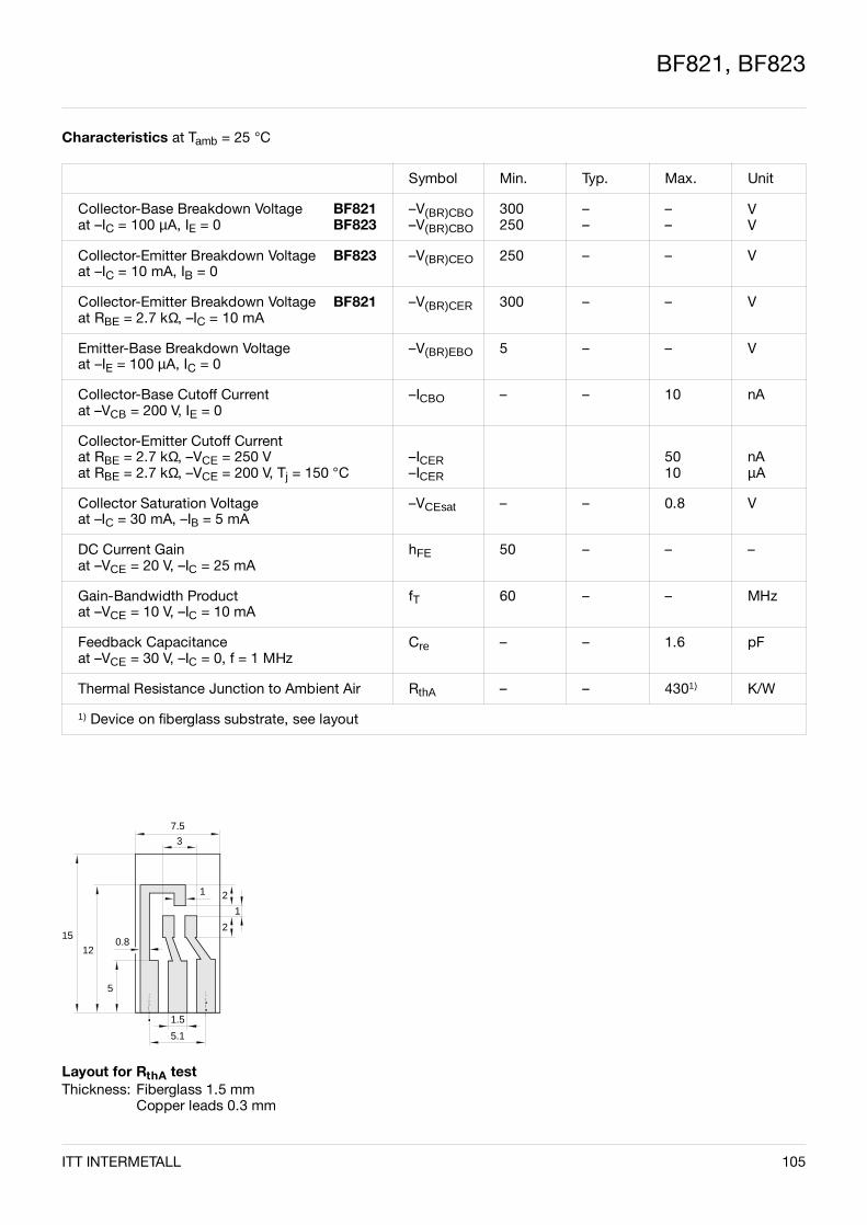
BF821, BF823
Characteristics at Tamb = 25 °C
Symbol Min. Typ. Max. Unit
Collector-Base Breakdown Voltage BF821at –IC = 100 µA, IE = 0 BF823
–V(BR)CBO–V(BR)CBO
300250
––
––
VV
Collector-Emitter Breakdown Voltage BF823at –IC = 10 mA, IB = 0
–V(BR)CEO 250 – – V
Collector-Emitter Breakdown Voltage BF821at RBE = 2.7 kΩ, –IC = 10 mA
–V(BR)CER 300 – – V
Emitter-Base Breakdown Voltageat –IE = 100 µA, IC = 0
–V(BR)EBO 5 – – V
Collector-Base Cutoff Currentat –VCB = 200 V, IE = 0
–ICBO – – 10 nA
Collector-Emitter Cutoff Currentat RBE = 2.7 kΩ, –VCE = 250 Vat RBE = 2.7 kΩ, –VCE = 200 V, Tj = 150 °C
–ICER–ICER
5010
nAµA
Collector Saturation Voltageat –IC = 30 mA, –IB = 5 mA
–VCEsat – – 0.8 V
DC Current Gainat –VCE = 20 V, –IC = 25 mA
hFE 50 – – –
Gain-Bandwidth Productat –VCE = 10 V, –IC = 10 mA
fT 60 – – MHz
Feedback Capacitanceat –VCE = 30 V, –IC = 0, f = 1 MHz
Cre – – 1.6 pF
Thermal Resistance Junction to Ambient Air RthA – – 4301) K/W
1) Device on fiberglass substrate, see layout
Layout for RthA testThickness: Fiberglass 1.5 mm
Copper leads 0.3 mm
15 12
5
0.8
7.5
3
1
1.5
5.1
2
2
1
ITT INTERMETALL 105
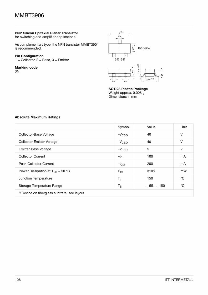
MMBT3906
PNP Silicon Epitaxial Planar Transistorfor switching and amplifier applications.
As complementary type, the NPN transistor MMBT3904 is recommended.
Pin Configuration1 = Collector, 2 = Base, 3 = Emitter.
Marking code3N
0.4
0.95 0.95
3
0.4 0.4
+0.1
1
2 3
Top View
SOT-23 Plastic PackageWeight approx. 0.008 gDimensions in mm
2.45+0.1
Absolute Maximum Ratings
Symbol Value Unit
Collector-Base Voltage –VCBO 40 V
Collector-Emitter Voltage –VCEO 40 V
Emitter-Base Voltage –VEBO 5 V
Collector Current –IC 100 mA
Peak Collector Current –ICM 200 mA
Power Dissipation at TSB = 50 °C Ptot 3101) mW
Junction Temperature Tj 150 °C
Storage Temperature Range TS –55…+150 °C
1) Device on fiberglass subtrate, see layout
106 ITT INTERMETALL
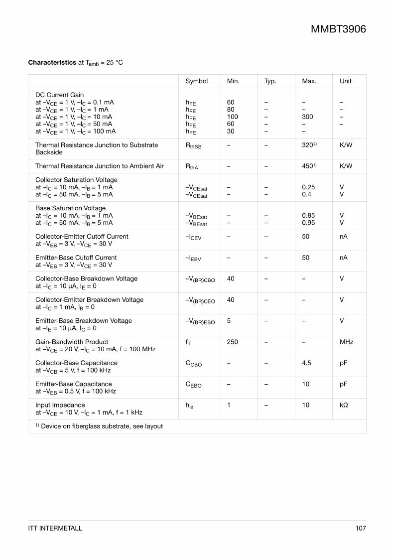
MMBT3906
Characteristics at Tamb = 25 °C
Symbol Min. Typ. Max. Unit
DC Current Gainat –VCE = 1 V, –IC = 0.1 mAat –VCE = 1 V, –IC = 1 mAat –VCE = 1 V, –IC = 10 mAat –VCE = 1 V, –IC = 50 mAat –VCE = 1 V, –IC = 100 mA
hFEhFEhFEhFEhFE
60801006030
–––––
––300––
––––
Thermal Resistance Junction to SubstrateBackside
RthSB – – 3201) K/W
Thermal Resistance Junction to Ambient Air RthA – – 4501) K/W
Collector Saturation Voltageat –IC = 10 mA, –IB = 1 mAat –IC = 50 mA, –IB = 5 mA
–VCEsat–VCEsat
––
––
0.250.4
VV
Base Saturation Voltageat –IC = 10 mA, –IB = 1 mAat –IC = 50 mA, –IB = 5 mA
–VBEsat–VBEsat
––
––
0.850.95
VV
Collector-Emitter Cutoff Currentat –VEB = 3 V, –VCE = 30 V
–ICEV – – 50 nA
Emitter-Base Cutoff Currentat –VEB = 3 V, –VCE = 30 V
–IEBV – – 50 nA
Collector-Base Breakdown Voltageat –IC = 10 µA, IE = 0
–V(BR)CBO 40 – – V
Collector-Emitter Breakdown Voltageat –IC = 1 mA, IB = 0
–V(BR)CEO 40 – – V
Emitter-Base Breakdown Voltageat –IE = 10 µA, IC = 0
–V(BR)EBO 5 – – V
Gain-Bandwidth Productat –VCE = 20 V, –IC = 10 mA, f = 100 MHz
fT 250 – – MHz
Collector-Base Capacitanceat –VCB = 5 V, f = 100 kHz
CCBO – – 4.5 pF
Emitter-Base Capacitanceat –VEB = 0.5 V, f = 100 kHz
CEBO – – 10 pF
Input Impedance at –VCE = 10 V, –IC = 1 mA, f = 1 kHz
hie 1 – 10 kΩ
1) Device on fiberglass substrate, see layout
ITT INTERMETALL 107
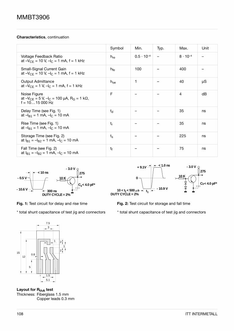
MMBT3906
Characteristics, continuation
Fig. 1: Test circuit for delay and rise time Fig. 2: Test circuit for storage and fall time
* total shunt capacitance of test jig and connectors * total shunt capacitance of test jig and connectors
Symbol Min. Typ. Max. Unit
Voltage Feedback Ratio at –VCE = 10 V, –IC = 1 mA, f = 1 kHz
hre 0.5 · 10–4 – 8 · 10–4 –
Small-Signal Current Gain at –VCE = 10 V, –IC = 1 mA, f = 1 kHz
hfe 100 – 400 –
Output Admittanceat –VCE = 1 V, –IC = 1 mA, f = 1 kHz
hoe 1 – 40 µS
Noise Figureat –VCE = 5 V, –IC = 100 µA, RG = 1 kΩ,f = 10…15 000 Hz
F – – 4 dB
Delay Time (see Fig. 1)at –IB1 = 1 mA, –IC = 10 mA
td – – 35 ns
Rise Time (see Fig. 1)at –IB1 = 1 mA, –IC = 10 mA
tr – – 35 ns
Storage Time (see Fig. 2)at IB1 = –IB2 = 1 mA, –IC = 10 mA
ts – – 225 ns
Fall Time (see Fig. 2)at IB1 = –IB2 = 1 mA, –IC = 10 mA
tf – – 75 ns
300 nsDUTY CYCLE = 2%
- 0.5 V
- 10.6 V
< 10 ns- 3.0 V
27510 K
C < 4.0 pF*3
0
+ 9.1V - 3.0 V275
10 K
C < 4.0 pF*3
10 < t < 500 msDUTY CYCLE = 2%
- 10.9 Vt11
< 1.0 ns
Layout for RthA testThickness: Fiberglass 1.5 mm
Copper leads 0.3 mm
15 12
5
0.8
7.5
3
1
1.5
5.1
2
2
1
108 ITT INTERMETALL

MMBT3906
ITT INTERMETALL 109

MMBTA92, MMBTA93
PNP Silicon Epitaxial Planar Transistorsespecially suited as line switch in telephone subsetsand in video output stages of TV receivers and moni-tors.
As complementary types, the PNP transistors MMBTA42and MMBTA43 are recommended.
Pin Configuration1 = Collector, 2 = Base, 3 = Emitter
Marking CodeMMBTA92 = 2DMMBTA93 = 2E
0.4
0.95 0.95
3
0.4 0.4
+0.1
1
2 3
Top View
SOT-23 Plastic PackageWeight approx. 0.008 gDimensions in mm
2.45+0.1
Absolute Maximum Ratings
Symbol Value Unit
Collector-Emitter Voltage MMBTA92MMBTA93
–VCEO–VCEO
300200
VV
Collector-Base Voltage MMBTA92MMBTA93
–VCBO–VCBO
300200
VV
Emitter-Base Voltage –VEBO 5 V
Collector Current –IC 500 mA
Power Dissipation1) at TSB = 50 °C Ptot 3001) mW
Junction Temperature Tj 150 °C
Storage Temperature Range TS –65…+150 °C
1) Device on fiberglass substrate, see layout
110 ITT INTERMETALL
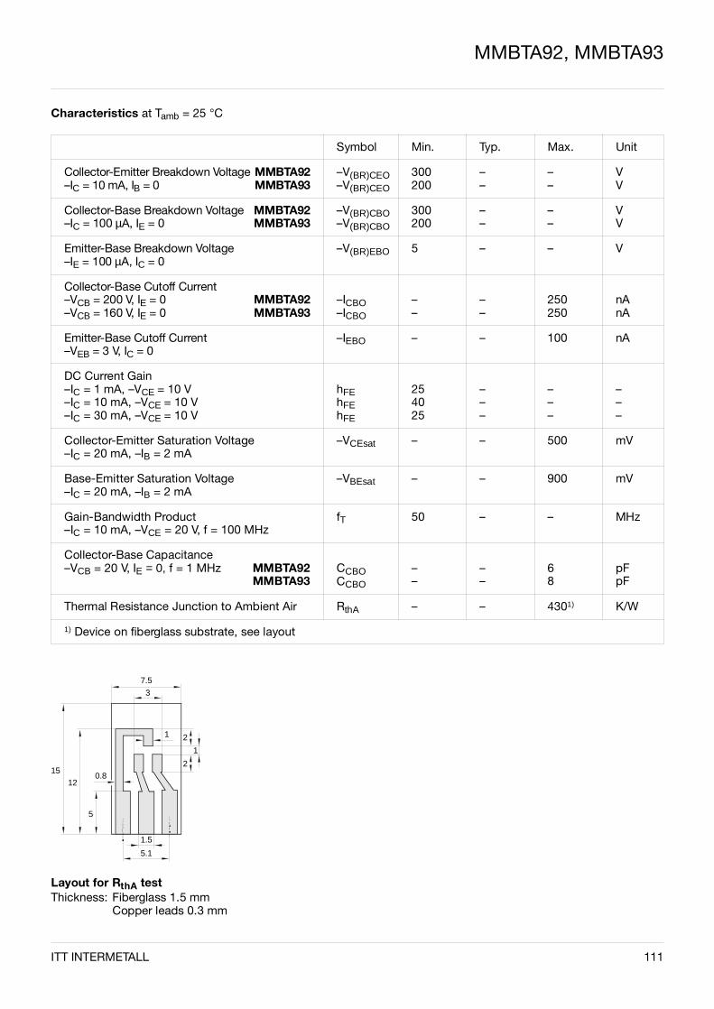
MMBTA92, MMBTA93
Characteristics at Tamb = 25 °C
Symbol Min. Typ. Max. Unit
Collector-Emitter Breakdown Voltage MMBTA92–IC = 10 mA, IB = 0 MMBTA93
–V(BR)CEO–V(BR)CEO
300200
––
––
VV
Collector-Base Breakdown Voltage MMBTA92–IC = 100 µA, IE = 0 MMBTA93
–V(BR)CBO–V(BR)CBO
300200
––
––
VV
Emitter-Base Breakdown Voltage–IE = 100 µA, IC = 0
–V(BR)EBO 5 – – V
Collector-Base Cutoff Current–VCB = 200 V, IE = 0 MMBTA92–VCB = 160 V, IE = 0 MMBTA93
–ICBO–ICBO
––
––
250250
nAnA
Emitter-Base Cutoff Current–VEB = 3 V, IC = 0
–IEBO – – 100 nA
DC Current Gain–IC = 1 mA, –VCE = 10 V–IC = 10 mA, –VCE = 10 V–IC = 30 mA, –VCE = 10 V
hFEhFEhFE
254025
–––
–––
–––
Collector-Emitter Saturation Voltage–IC = 20 mA, –IB = 2 mA
–VCEsat – – 500 mV
Base-Emitter Saturation Voltage–IC = 20 mA, –IB = 2 mA
–VBEsat – – 900 mV
Gain-Bandwidth Product–IC = 10 mA, –VCE = 20 V, f = 100 MHz
fT 50 – – MHz
Collector-Base Capacitance–VCB = 20 V, IE = 0, f = 1 MHz MMBTA92
MMBTA93CCBOCCBO
––
––
68
pFpF
Thermal Resistance Junction to Ambient Air RthA – – 4301) K/W
1) Device on fiberglass substrate, see layout
Layout for RthA testThickness: Fiberglass 1.5 mm
Copper leads 0.3 mm
15 12
5
0.8
7.5
3
1
1.5
5.1
2
2
1
ITT INTERMETALL 111

MPSA92, MPSA93
PNP Silicon Epitaxial Planar Transistorsespecially suited as line switch in telephone subsetsand in video output stages of TV receivers and moni-tors.
As complementary types, the PNP transistors MPSA42and MPSA43 are recommended.
0.55∅ max.
2.5
B
CE
4.6 3.6
TO-92 Plastic PackageWeight approx. 0.18 gDimensions in mm
Absolute Maximum Ratings
Symbol Value Unit
Collector-Emitter Voltage MPSA92MPSA93
–VCEO–VCEO
300200
VV
Collector-Base Voltage MPSA92MPSA93
–VCBO–VCBO
300200
VV
Emitter-Base Voltage –VEBO 5 V
Collector Current –IC 500 mA
Power Dissipation at Tamb = 25 °C Ptot 6251) mW
Junction Temperature Tj 150 °C
Storage Temperature Range TS –65…+150 °C
1) Valid provided that lead are kept at ambient temperature at a distance of 2 mm from case.
112 ITT INTERMETALL
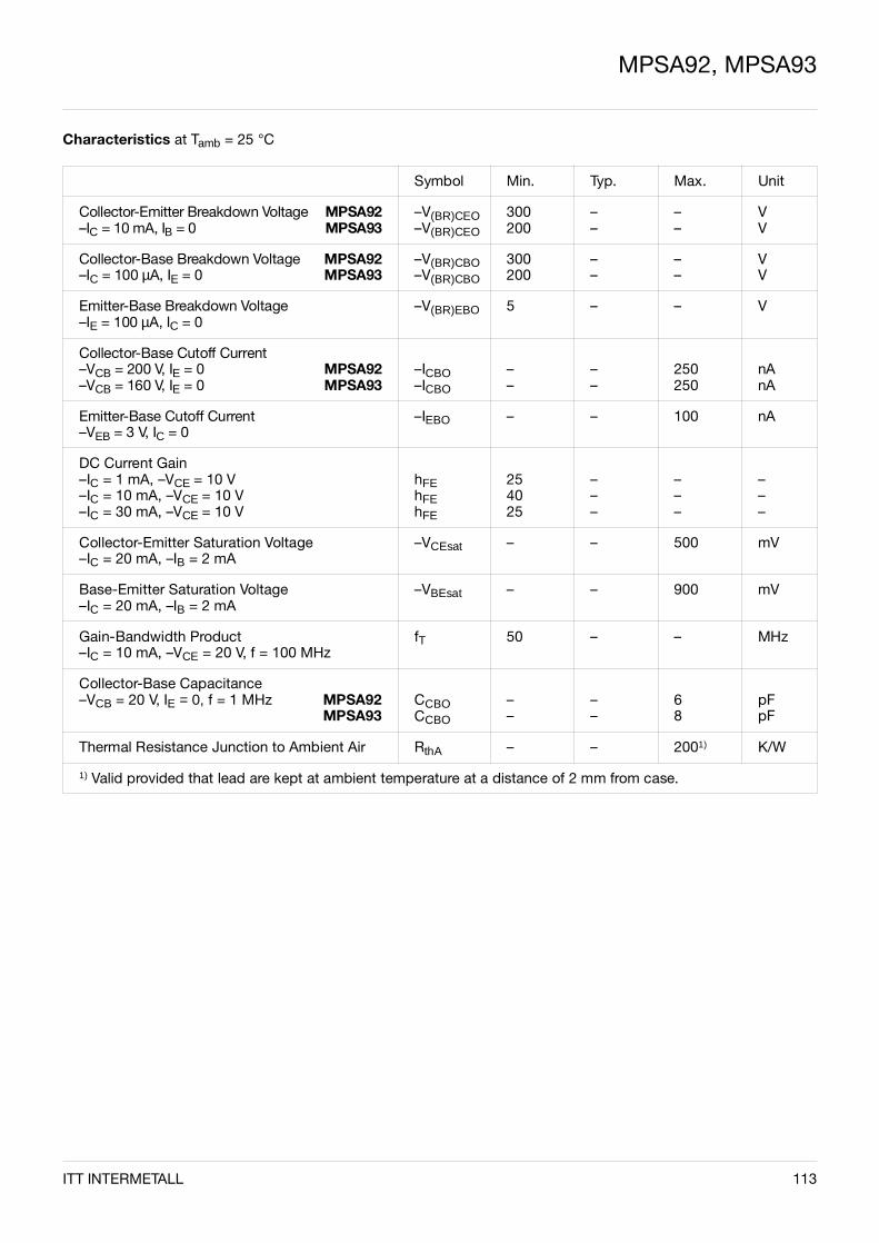
MPSA92, MPSA93
Characteristics at Tamb = 25 °C
Symbol Min. Typ. Max. Unit
Collector-Emitter Breakdown Voltage MPSA92–IC = 10 mA, IB = 0 MPSA93
–V(BR)CEO–V(BR)CEO
300200
––
––
VV
Collector-Base Breakdown Voltage MPSA92–IC = 100 µA, IE = 0 MPSA93
–V(BR)CBO–V(BR)CBO
300200
––
––
VV
Emitter-Base Breakdown Voltage–IE = 100 µA, IC = 0
–V(BR)EBO 5 – – V
Collector-Base Cutoff Current–VCB = 200 V, IE = 0 MPSA92–VCB = 160 V, IE = 0 MPSA93
–ICBO–ICBO
––
––
250250
nAnA
Emitter-Base Cutoff Current–VEB = 3 V, IC = 0
–IEBO – – 100 nA
DC Current Gain–IC = 1 mA, –VCE = 10 V–IC = 10 mA, –VCE = 10 V–IC = 30 mA, –VCE = 10 V
hFEhFEhFE
254025
–––
–––
–––
Collector-Emitter Saturation Voltage–IC = 20 mA, –IB = 2 mA
–VCEsat – – 500 mV
Base-Emitter Saturation Voltage–IC = 20 mA, –IB = 2 mA
–VBEsat – – 900 mV
Gain-Bandwidth Product–IC = 10 mA, –VCE = 20 V, f = 100 MHz
fT 50 – – MHz
Collector-Base Capacitance–VCB = 20 V, IE = 0, f = 1 MHz MPSA92
MPSA93CCBOCCBO
––
––
68
pFpF
Thermal Resistance Junction to Ambient Air RthA – – 2001) K/W
1) Valid provided that lead are kept at ambient temperature at a distance of 2 mm from case.
ITT INTERMETALL 113

114 ITT INTERMETALL
DMOS Transistors (N-Channel)
ITT INTERMETALL 115

2N7000
N-Channel Enhancement Mode DMOS Transistor
Features– high input impedance– low gate threshold voltage– low drain-source ON resistance– high-speed switching– no minority carrier storage time– CMOS logic compatible input– no thermal runaway– no secondary breakdown
TO-92 Plastic PackageWeight approx. 0.18 gDimensions in mm
0.55∅ max.
2.5
G
DS
4.6 3.6
Absolute Maximum Ratings
Inverse Diode
Symbol Value Unit
Drain-Source Voltage VDSS 60 V
Drain-Gate Voltage VDGS 60 V
Gate-Source Voltage (pulsed) VGS ± 20 V
Drain Current (continuous) ID 300 mA
Power Dissipation at Tamb = 25 °C Ptot 8301) mW
Junction Temperature Tj 150 °C
Storage Temperature Range TS –65…+150 °C
1) Valid provided that leads are kept at ambient temperature at a distance of 2 mm from case.
Symbol Value Unit
Max. Forward Current (continuous)at Tamb = 25 °C
IF 500 mA
Forward Voltage Drop (typ.)at VGS = 0, IF = 0.5 A, Tj = 25 °C
VF 850 mV
116 ITT INTERMETALL
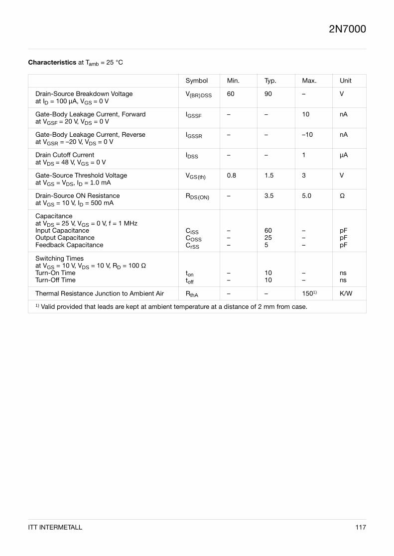
2N7000
Characteristics at Tamb = 25 °C
Symbol Min. Typ. Max. Unit
Drain-Source Breakdown Voltageat ID = 100 µA, VGS = 0 V
V(BR)DSS 60 90 – V
Gate-Body Leakage Current, Forwardat VGSF = 20 V, VDS = 0 V
IGSSF – – 10 nA
Gate-Body Leakage Current, Reverseat VGSR = –20 V, VDS = 0 V
IGSSR – – –10 nA
Drain Cutoff Current at VDS = 48 V, VGS = 0 V
IDSS – – 1 µA
Gate-Source Threshold Voltageat VGS = VDS, ID = 1.0 mA
VGS(th) 0.8 1.5 3 V
Drain-Source ON Resistanceat VGS = 10 V, ID = 500 mA
RDS(ON) – 3.5 5.0 Ω
Capacitanceat VDS = 25 V, VGS = 0 V, f = 1 MHzInput CapacitanceOutput CapacitanceFeedback Capacitance
CiSSCOSSCrSS
–––
60255
–––
pFpFpF
Switching Timesat VGS = 10 V, VDS = 10 V, RD = 100 ΩTurn-On TimeTurn-Off Time
tontoff
––
1010
––
nsns
Thermal Resistance Junction to Ambient Air RthA – – 1501) K/W
1) Valid provided that leads are kept at ambient temperature at a distance of 2 mm from case.
ITT INTERMETALL 117
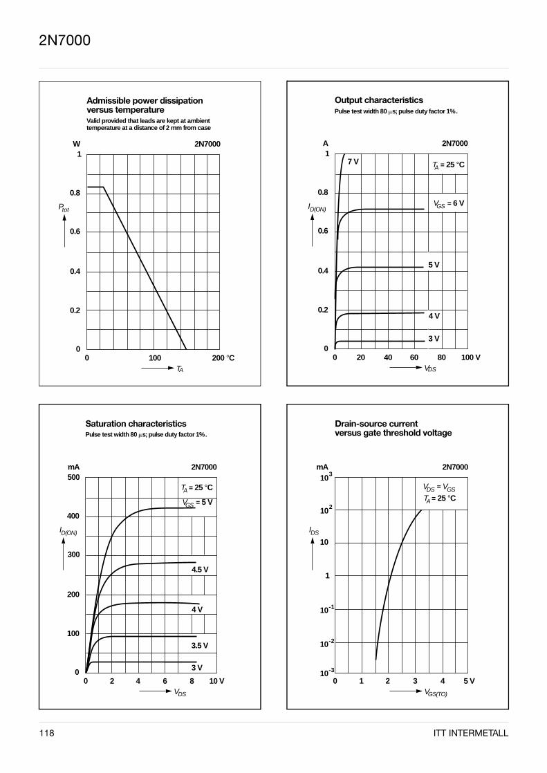
118 ITT INTERMETALL
2N7000
Output characteristics
A1
0.6
0.4
4000
0.2
VDS
100 V
Pulse test width 80 ms; pulse duty factor 1%.
2N7000
0.8
20 60 80
ID(ON)
T = 25 °CA
V = 6 VGS
5 V
4 V
3 V
7 V
Admissible power dissipation versus temperature
W1
Ptot
0.6
0.4
10000
0.2
TA
200 °C
Valid provided that leads are kept at ambient temperature at a distance of 2 mm from case
2N7000
0.8
Saturation characteristics
mA500
ID(ON)
300
200
600
100
VDS
10 V
Pulse test width 80 ms; pulse duty factor 1%.
2N7000
400
T = 25 °CA
V = 5 VGS
2 4 8
3 V
3.5 V
4 V
4.5 V
Drain-source current versus gate threshold voltage
mA
0VGS(TO)
5 V
2N7000
10
1
10-1
103
102
10-2
10-3
1 2 3 4
IDS
V = VDS GS
T = 25 °CA
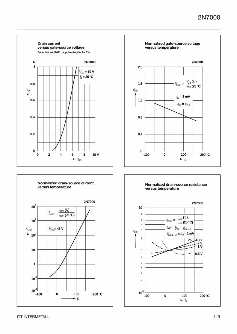
ITT INTERMETALL 119
Normalized drain-source resistance versus temperature
10
1
-100TA
200 °C
2N7000
10-1
0
rDSn
7
5
4
3
2
7
5
4
3
2
100
rDS (T )A
(25 °C)r =DSn rDS
∆V = V – V GS
GS (TO)V at I = 1 mAD
>3 V2 V1 V
0.5 V
∆V
GS(TO)
2N7000
Normalized gate-source voltage versus temperature
VGS
-100TA
200 °C
2N70002.0
100
n
VGS (T )A
(25 °C)
I = 1 mAD
1.6
1.2
0.8
0.4
00
V =GSn VGS
V = DS VGS
Normalized drain-source current versus temperature
-100TA
200 °C
2N7000104
103
102
10
1
10-2
0 100
IDSn
IDS (T )A
IDS (25 °C)
V = 45 VDS
10-1
I =DSn
Drain current versus gate-source voltage
A1
ID
0.6
0.4
00
0.2
VGS
10 V
Pulse test width 80 ms; pulse duty factor 1%.
2N7000
0.8
2 4 6 8
V = 10 VDS
T = 25 °CA
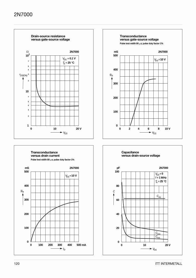
120 ITT INTERMETALL
2N7000
Transconductance versus gate-source voltage
mS500
gfs
00
VGS
10 V
Pulse test width 80 ms; pulse duty factor 1%
2N7000
400
300
200
100
2 4 6 8
V = 10 VDS
Transconductance versus drain current
mS500
gfs
00
ID
500 mA
Pulse test width 80 ms; pulse duty factor 1%
2N7000
400
300
200
100
100 200 300 400
V = 10 VDS
Capacitance versus drain-source voltage
pF100
C
1000
VDS
20 V
2N7000
80
60
40
20
V = 0GSf = 1 MHzT = 25 °CA
Ciss
CossCrss
Drain-source resistance versus gate-source voltage
V
rDS(ON)
1001
VGS
20 V
2N7000102
7
5
4
3
2
10
7
5
4
3
2
V = 0.1 VDS
T = 25 °CA

ITT INTERMETALL 121
2N7000
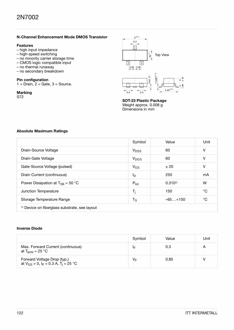
2N7002
N-Channel Enhancement Mode DMOS Transistor
Features– high input impedance– high-speed switching– no minority carrier storage time– CMOS logic compatible input– no thermal runaway– no secondary breakdown
Pin configuration1 = Drain, 2 = Gate, 3 = Source.
Marking S72
0.4
0.95 0.95
3
0.4 0.4
+0.1
1
2 3
Top View
SOT-23 Plastic PackageWeight approx. 0.008 gDimensions in mm
2.45+0.1
Absolute Maximum RatingsAbsolute Maximum Ratings
Inverse Diode
Symbol Value Unit
Drain-Source Voltage VDSS 60 V
Drain-Gate Voltage VDGS 60 V
Gate-Source-Voltage (pulsed) VGS ±20 V
Drain Current (continuous) ID 250 mA
Power Dissipation at TC = 50 °C Ptot 0.3101) W
Junction Temperature Tj 150 °C
Storage Temperature Range TS –55 …+150 °C
1) Ceramic Substrate 0.7mm; 2.5 cm2 area.
Symbol Value Unit
Max. Forward Current (continuous)at Tamb = 25 °C
IF 0.3 A
Forward Voltage Drop (typ.)at VGS = 0, IF = 0.3 A, Tj = 25 °C
VF 0.85 V
Symbol Value Unit
Drain-Source Voltage VDSS 60 V
Drain-Gate Voltage VDGS 60 V
Gate-Source Voltage (pulsed) VGS ± 20 V
Drain Current (continuous) ID 250 mA
Power Dissipation at TSB = 50 °C Ptot 0.3101) W
Junction Temperature Tj 150 °C
Storage Temperature Range TS –65…+150 °C
1) Device on fiberglass substrate, see layout
122 ITT INTERMETALL
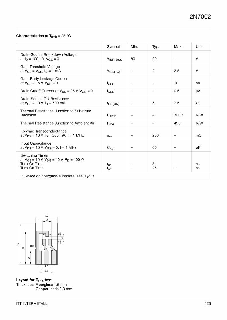
2N7002
Characteristics at Tamb = 25 °C
Symbol Min. Typ. Max. Unit
Drain-Source Breakdown Voltageat ID = 100 µA, VGS = 0 V(BR)DSS 60 90 – V
Gate Threshold Voltageat VGS = VDS, ID = 1 mA VGS(TO) – 2 2.5 V
Gate-Body Leakage Currentat VGS = 15 V, VDS = 0 IGSS – – 10 nA
Drain Cutoff Current at VDS = 25 V, VGS = 0 IDSS – – 0.5 µA
Drain-Source ON Resistanceat VGS = 10 V, ID = 500 mA rDS(ON) – 5 7.5 Ω
Thermal Resistance Junction to SubstrateBackside RthSB – – 3201) K/W
Thermal Resistance Junction to Ambient Air RthA – – 4501) K/W
Forward Transconductanceat VDS = 10 V, ID = 200 mA, f = 1 MHz gm – 200 – mS
Input Capacitanceat VDS = 10 V, VGS = 0, f = 1 MHz Ciss – 60 – pF
Switching Timesat VGS = 10 V, VDS = 10 V, RD = 100 ΩTurn-On TimeTurn-Off Time
tontoff
––
525
––
nsns
1) Device on fiberglass substrate, see layout
Layout for RthA testThickness: Fiberglass 1.5 mm
Copper leads 0.3 mm
15 12
5
0.8
7.5
3
1
1.5
5.1
2
2
1
ITT INTERMETALL 123
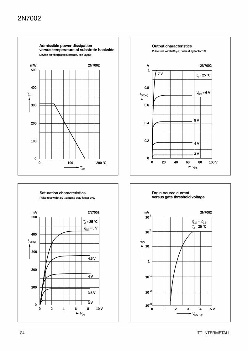
124 ITT INTERMETALL
2N7002
Admissible power dissipation versus temperature of substrate backside
mW500
Ptot
300
200
10000
100
TSB
200 °C
Device on fiberglass substrate, see layout
2N7002
400
Saturation characteristics
mA500
ID(ON)
300
200
600
100
VDS
10 V
Pulse test width 80 ms; pulse duty factor 1%.
2N7002
400
T = 25 °CA
V = 5 VGS
2 4 8
3 V
3.5 V
4 V
4.5 V
Output characteristics
A1
0.6
0.4
4000
0.2
VDS
100 V
Pulse test width 80 ms; pulse duty factor 1%.
2N7002
0.8
20 60 80
ID(ON)
T = 25 °CA
V = 6 VGS
5 V
4 V
3 V
7 V
Drain-source current versus gate threshold voltage
mA
0VGS(TO)
5 V
2N7002
10
1
10-1
103
102
10-2
10-3
1 2 3 4
IDS
V = VDS GS
T = 25 °CA
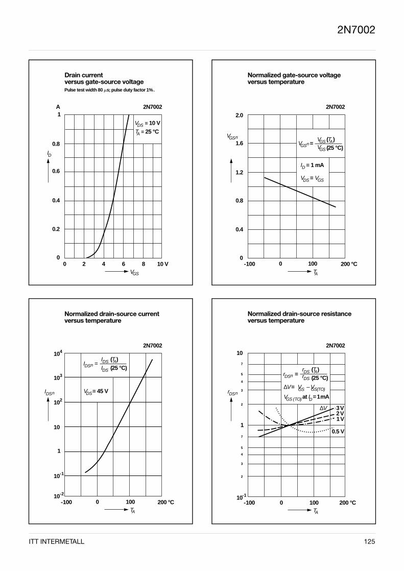
ITT INTERMETALL 125
2N7002
Drain current versus gate-source voltage
A1
ID
0.6
0.4
00
0.2
VGS
10 V
Pulse test width 80 ms; pulse duty factor 1%.
2N7002
0.8
2 4 6 8
V = 10 VDS
T = 25 °CA
Normalized drain-source current versus temperature
-100TA
200 °C
2N7002104
103
102
10
1
10-2
0 100
IDSn
IDS (T )A
IDS (25 °C)
V = 45 VDS
10-1
I =DSn
Normalized gate-source voltage versus temperature
VGS
-100TA
200 °C
2N70022.0
100
n VGS (T )A
(25 °C)
I = 1 mAD
1.6
1.2
0.8
0.4
00
V =GSnVGS
V = DS VGS
Normalized drain-source resistance versus temperature
10
1
-100TA
200 °C
2N7002
10-1
0
rDSn
7
5
4
3
2
7
5
4
3
2
100
rDS (T )A
(25 °C)r =DSn rDS
∆V = V – V GS
GS (TO)V at I = 1 mAD
3 V2 V1 V
0.5 V
∆V
GS(TO)
&
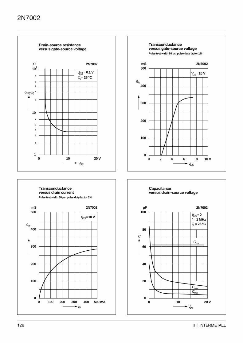
126 ITT INTERMETALL
2N7002
Drain-source resistance versus gate-source voltage
V
rDS(ON)
1001
VGS
20 V
2N7002102
7
5
4
3
2
10
7
5
4
3
2
V = 0.1 VDST = 25 °CA
Transconductance versus drain current
mS500
gfs
00
ID
500 mA
Pulse test width 80 ms; pulse duty factor 1%
2N7002
400
300
200
100
100 200 300 400
V = 10 VDS
Transconductance versus gate-source voltage
mS500
gfs
00
VGS
10 V
Pulse test width 80 ms; pulse duty factor 1%
2N7002
400
300
200
100
2 4 6 8
V = 10 VDS
Capacitance versus drain-source voltage
pF100
C
1000
VDS
20 V
2N7002
80
60
40
20
V = 0GSf = 1 MHzT = 25 °CA
Ciss
CossCrss

ITT INTERMETALL 127
2N7002
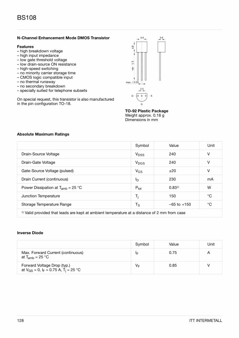
BS108
N-Channel Enhancement Mode DMOS Transistor
Features– high breakdown voltage– high input impedance– low gate threshold voltage– low drain-source ON resistance– high-speed switching– no minority carrier storage time– CMOS logic compatible input– no thermal runaway– no secondary breakdown– specially suited for telephone subsets
On special request, this transistor is also manufacturedin the pin configuration TO-18.
0.55∅ max.
2.5
G
SD
4.6 3.6
TO-92 Plastic PackageWeight approx. 0.18 gDimensions in mm
Absolute Maximum Ratings
Symbol Value Unit
Drain-Source Voltage VDSS 240 V
Drain-Gate Voltage VDGS 240 V
Gate-Source Voltage (pulsed) VGS ±20 V
Drain Current (continuous) ID 230 mA
Power Dissipation at Tamb = 25 °C Ptot 0.831) W
Junction Temperature Tj 150 °C
Storage Temperature Range TS –65 to +150 °C
1) Valid provided that leads are kept at ambient temperature at a distance of 2 mm from case
Inverse Diode
Symbol Value Unit
Max. Forward Current (continuous)at Tamb = 25 °C
IF 0.75 A
Forward Voltage Drop (typ.)at VGS = 0, IF = 0.75 A, Tj = 25 °C
VF 0.85 V
128 ITT INTERMETALL

BS108
Characteristics at Tamb = 25 °C
Symbol Min. Typ. Max. Unit
Drain-Source Breakdown Voltageat ID = 100 µA, VGS = 0
V(BR)DSS 240 250 – V
Gate-Body Leakage Currentat VGS = 15 V, VDS = 0
IGSS – – 10 nA
Drain Cutoff Currentat VDS = 130 V, VGS = 0at VDS = 70 V, VGS = 0.2 V
IDSSIDSX
––
––
125
µAµA
Gate-Source Threshold Voltageat VGS = VDS, ID = 1 mA
VGS(TO) 0.8 1.5 2.5 V
Drain-Source ON Resistanceat VGS = 2.8 V, ID = 100 mA
RDS(ON) – 5.5 8 Ω
Thermal Resistance Junction to Ambient Air RthA – – 1501) K/W
Capacitanceat VDS = 20 V, VGS = 0, f = 1 MHzInput CapacitanceOutput CapacitanceFeedback Capacitance
CiSSCOSSCrSS
–––
80205
–––
pFpFpF
Switching Timesat VGS = 10 V, VDS = 10 V, RD = 100 ΩTurn-On TimeTurn-Off Time
tontoff
––
550
––
nsns
1) Valid provided that leads are kept at ambient temperature at a distance of 2 mm from case
ITT INTERMETALL 129
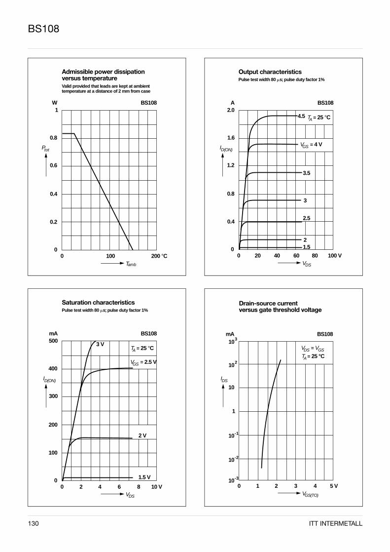
130 ITT INTERMETALL
BS108
Admissible power dissipation versus temperature
W1
Ptot
0.6
0.4
10000
0.2
Tamb
200 °C
Valid provided that leads are kept at ambient temperature at a distance of 2 mm from case
BS108
0.8
Output characteristics
A2.0
ID(ON)
1.2
0.8
6000
0.4
VDS
100 V
Pulse test width 80 ms; pulse duty factor 1%
BS108
1.6
T = 25 °CA
V = 4 VGS
20 40 80
3
3.5
2
4.5
2.5
1.5
Saturation characteristics
mA500
ID(ON)
300
200
600
100
VDS
10 V
Pulse test width 80 ms; pulse duty factor 1%
BS108
400
T = 25 °CA
V = 2.5 VGS
2 4 8
1.5 V
2 V
3 V
Drain-source current versus gate threshold voltage
mA
0VGS(TO)
5 V
BS108
10
1
10-1
103
102
10-2
10-3
1 2 3 4
IDS
V = VDS GS
T = 25 °CA
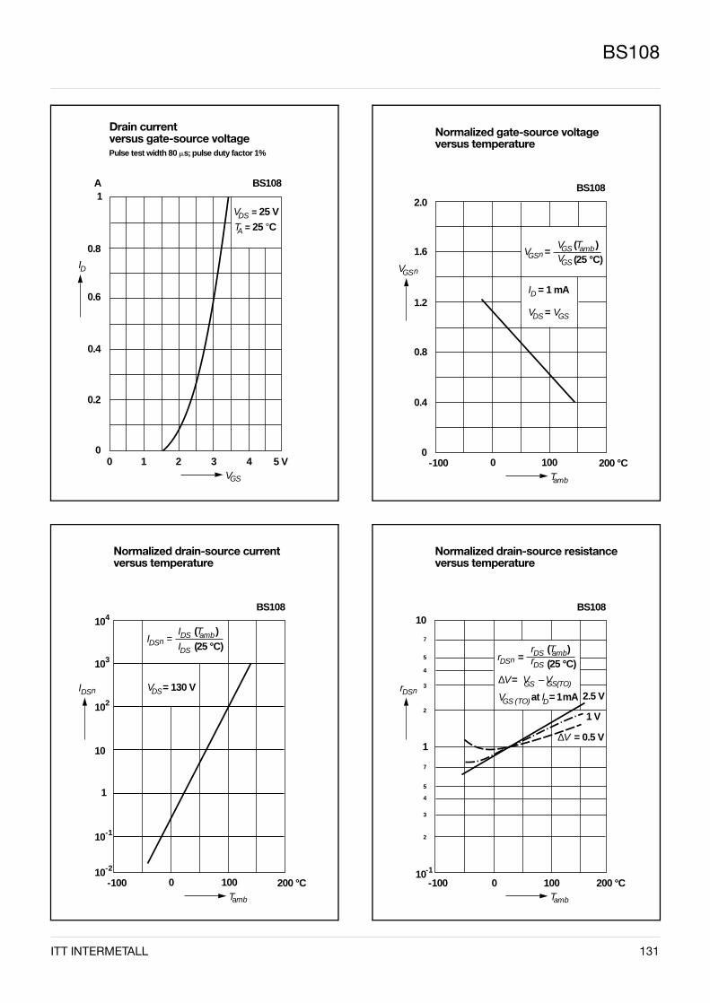
ITT INTERMETALL 131
BS108
Normalized gate-source voltage versus temperature
VGS
-100Tamb
200 °C
BS1082.0
100
n
VGS (T )amb
(25 °C)
I = 1 mAD
1.6
1.2
0.8
0.4
00
V =GSn VGS
V = DS VGS
Drain current versus gate-source voltage
A1
ID
0.6
0.4
00
0.2
VGS
5 V
Pulse test width 80 ms; pulse duty factor 1%
BS108
0.8
1 2 3 4
V = 25 VDS
T = 25 °CA
Normalized drain-source current versus temperature
-100Tamb
200 °C
BS108104
103
102
10
1
10-2
0 100
IDSn
IDS (T )amb
IDS (25 °C)
V = 130 VDS
10-1
I =DSn
Normalized drain-source resistance versus temperature
10
1
-100Tamb
200 °C
BS108
10-1
0
rDSn
7
5
4
3
2
7
5
4
3
2
100
rDS (T )amb
(25 °C)r =DSn rDS
∆V = V – V GS
GS (TO)V at I = 1 mAD2.5 V
1 V
= 0.5 V∆V
GS(TO)
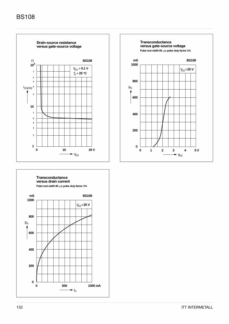
132 ITT INTERMETALL
BS108
Transconductance versus gate-source voltage
mS1000
gfs
00
VGS
Pulse test width 80 ms; pulse duty factor 1%
BS108
800
600
400
200
V = 25 VDS
1 2 3 4 5 V
Drain-source resistance versus gate-source voltage
V
rDS(ON)
1001
VGS
20 V
BS108102
7
5
4
3
2
10
7
5
4
3
2
V = 0.1 VDS
T = 25 °CA
Transconductance versus drain current
mS1000
gfs
00
ID
1000 mA
Pulse test width 80 ms; pulse duty factor 1%
BS108
800
600
400
200
500
V = 25 VDS

ITT INTERMETALL 133
BS108

BS109
N-Channel Enhancement Mode DMOS Transistor
Features– high input impedance– low gate threshold voltage– low drain-source ON resistance– high-speed switching– no minority carrier storage time– CMOS logic compatible input– no thermal runaway– no secondary breakdown 0.55∅ max.
2.5
G
SD
4.6 3.6
TO-92 Plastic PackageWeight approx. 0.18 gDimensions in mm
Absolute Maximum Ratings
Symbol Value Unit
Drain-Source Voltage VDSS 400 V
Drain-Gate Voltage VDGS 400 V
Gate-Source Voltage (pulsed) VGS ±20 V
Drain Current (continuous) at Tamb = 25 °C ID 120 mA
Power Dissipation at Tamb = 25 °C Ptot 8301) mW
Junction Temperature Tj 150 °C
Storage Temperature Range TS –65 to +150 °C
1) Valid provided that leads are kept at ambient temperature at a distance of 2 mm from case.
Inverse Diode
Symbol Value Unit
Max. Forward Current (continuous)at Tamb = 25 °C
IF 400 mA
Forward Voltage Drop (typ.)at VGS = 0 V, IF = 400 mA, Tj = 25 °C
VF 1.0 V
134 ITT INTERMETALL
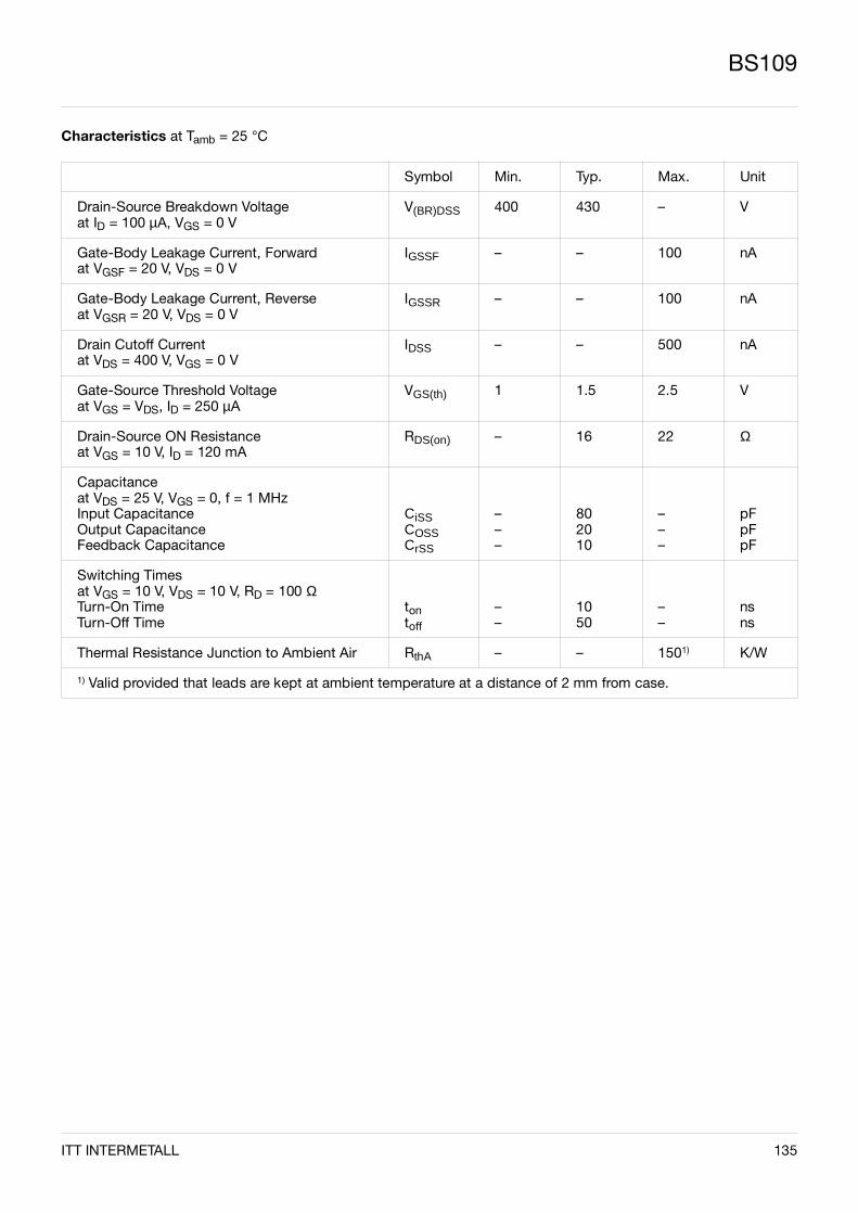
BS109
Characteristics at Tamb = 25 °C
Symbol Min. Typ. Max. Unit
Drain-Source Breakdown Voltageat ID = 100 µA, VGS = 0 V
V(BR)DSS 400 430 – V
Gate-Body Leakage Current, Forwardat VGSF = 20 V, VDS = 0 V
IGSSF – – 100 nA
Gate-Body Leakage Current, Reverseat VGSR = 20 V, VDS = 0 V
IGSSR – – 100 nA
Drain Cutoff Currentat VDS = 400 V, VGS = 0 V
IDSS – – 500 nA
Gate-Source Threshold Voltageat VGS = VDS, ID = 250 µA
VGS(th) 1 1.5 2.5 V
Drain-Source ON Resistanceat VGS = 10 V, ID = 120 mA
RDS(on) – 16 22 Ω
Capacitanceat VDS = 25 V, VGS = 0, f = 1 MHzInput CapacitanceOutput CapacitanceFeedback Capacitance
CiSSCOSSCrSS
–––
802010
–––
pFpFpF
Switching Timesat VGS = 10 V, VDS = 10 V, RD = 100 ΩTurn-On TimeTurn-Off Time
tontoff
––
1050
––
nsns
Thermal Resistance Junction to Ambient Air RthA – – 1501) K/W
1) Valid provided that leads are kept at ambient temperature at a distance of 2 mm from case.
ITT INTERMETALL 135
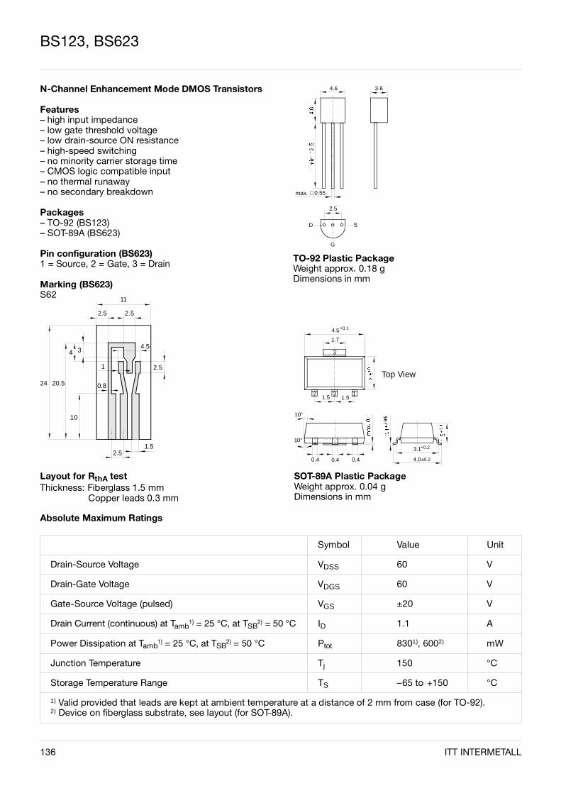
BS123, BS623
Thickness: Fiberglass 1.5 mmCopper leads 0.3 mm
Absolute Maximum Ratings
Symbol Value Unit
Drain-Source Voltage VDSS 60 V
Drain-Gate Voltage VDGS 60 V
Gate-Source Voltage (pulsed) VGS ±20 V
Drain Current (continuous) at Tamb1) = 25 °C, at TSB
2) = 50 °C ID 1.1 A
Power Dissipation at Tamb1) = 25 °C, at TSB
2) = 50 °C Ptot 8301), 6002) mW
Junction Temperature Tj 150 °C
Storage Temperature Range TS –65 to +150 °C
1) Valid provided that leads are kept at ambient temperature at a distance of 2 mm from case (for TO-92).2) Device on fiberglass substrate, see layout (for SOT-89A).
N-Channel Enhancement Mode DMOS Transistors
Features– high input impedance– low gate threshold voltage– low drain-source ON resistance– high-speed switching– no minority carrier storage time– CMOS logic compatible input– no thermal runaway– no secondary breakdown
Packages– TO-92 (BS123)– SOT-89A (BS623)
Pin configuration (BS623)1 = Source, 2 = Gate, 3 = Drain
Marking (BS623)S62
Layout for RthA test
2.51.5
11
2.5 2.5
24 20.5
10
4 3
0.8
1
4.5
2.5
136
0.55∅ max.
2.5
G
SD
4.6 3.6
TO-92 Plastic PackageWeight approx. 0.18 gDimensions in mm
SOT-89A Plastic PackageWeight approx. 0.04 gDimensions in mm
1.7
4.5
1.5 1.5
10°
0.40.4 0.4 4.0
3.1
±0.2
+0.1
10°+0.2
3
2 3 1
Top View
ITT INTERMETALL
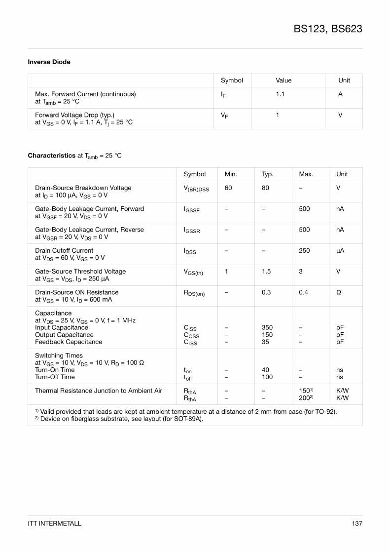
BS123, BS623
Characteristics at Tamb = 25 °C
Symbol Min. Typ. Max. Unit
Drain-Source Breakdown Voltageat ID = 100 µA, VGS = 0 V
V(BR)DSS 60 80 – V
Gate-Body Leakage Current, Forwardat VGSF = 20 V, VDS = 0 V
IGSSF – – 500 nA
Gate-Body Leakage Current, Reverseat VGSR = 20 V, VDS = 0 V
IGSSR – – 500 nA
Drain Cutoff Currentat VDS = 60 V, VGS = 0 V
IDSS – – 250 µA
Gate-Source Threshold Voltageat VGS = VDS, ID = 250 µA
VGS(th) 1 1.5 3 V
Drain-Source ON Resistanceat VGS = 10 V, ID = 600 mA
RDS(on) – 0.3 0.4 Ω
Capacitanceat VDS = 25 V, VGS = 0 V, f = 1 MHzInput CapacitanceOutput CapacitanceFeedback Capacitance
CiSSCOSSCrSS
–––
35015035
–––
pFpFpF
Switching Timesat VGS = 10 V, VDS = 10 V, RD = 100 ΩTurn-On TimeTurn-Off Time
tontoff
––
40100
––
nsns
Thermal Resistance Junction to Ambient Air RthARthA
––
––
1501)
2002)K/WK/W
1) Valid provided that leads are kept at ambient temperature at a distance of 2 mm from case (for TO-92).2) Device on fiberglass substrate, see layout (for SOT-89A).
Inverse Diode
Symbol Value Unit
Max. Forward Current (continuous)at Tamb = 25 °C
IF 1.1 A
Forward Voltage Drop (typ.)at VGS = 0 V, IF = 1.1 A, Tj = 25 °C
VF 1 V
ITT INTERMETALL 137
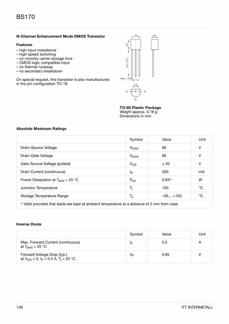
BS170
N-Channel Enhancement Mode DMOS Transistor
Features– high input impedance– high-speed switching– no minority carrier storage time– CMOS logic compatible input– no thermal runaway– no secondary breakdown
On special request, this transistor is also manufacturedin the pin configuration TO-18.
0.55∅ max.
2.5
G
SD
4.6 3.6
TO-92 Plastic PackageWeight approx. 0.18 gDimensions in mm
Absolute Maximum Ratings
Inverse Diode
Symbol Value Unit
Drain-Source Voltage VDSS 60 V
Drain-Gate Voltage VDGS 60 V
Gate-Source Voltage (pulsed) VGS ± 20 V
Drain Current (continuous) ID 300 mA
Power Dissipation at Tamb = 25 °C Ptot 0.831) W
Junction Temperature Tj 150 °C
Storage Temperature Range Ts –65…+150 °C
1) Valid provided that leads are kept at ambient temperature at a distance of 2 mm from case.
Symbol Value Unit
Max. Forward Current (continuous)at Tamb = 25 °C
IF 0.5 A
Forward Voltage Drop (typ.)at VGS = 0, IF = 0.5 A, Tj = 25 °C
VF 0.85 V
138 ITT INTERMETALL
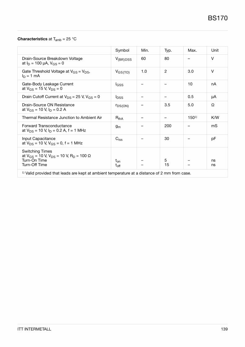
BS170
Characteristics at Tamb = 25 °C
Symbol Min. Typ. Max. Unit
Drain-Source Breakdown Voltageat ID = 100 µA, VGS = 0
V(BR)DSS 60 80 – V
Gate Threshold Voltage at VGS = VDS,ID = 1 mA
VGS(TO) 1.0 2 3.0 V
Gate-Body Leakage Currentat VGS = 15 V, VDS = 0
IGSS – – 10 nA
Drain Cutoff Current at VDS = 25 V, VGS = 0 IDSS – – 0.5 µA
Drain-Source ON Resistanceat VGS = 10 V, ID = 0.2 A
rDS(ON) – 3.5 5.0 Ω
Thermal Resistance Junction to Ambient Air RthA – – 1501) K/W
Forward Transconductanceat VDS = 10 V, ID = 0.2 A, f = 1 MHz
gm – 200 – mS
Input Capacitanceat VDS = 10 V, VGS = 0, f = 1 MHz
Ciss – 30 – pF
Switching Timesat VGS = 10 V, VDS = 10 V, RD = 100 ΩTurn-On TimeTurn-Off Time
tontoff
––
515
––
nsns
1) Valid provided that leads are kept at ambient temperature at a distance of 2 mm from case.
ITT INTERMETALL 139
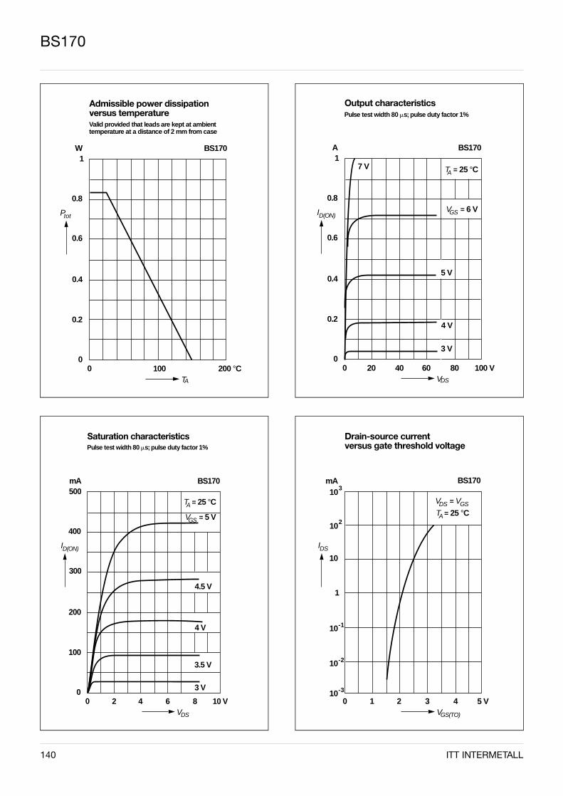
140 ITT INTERMETALL
Drain-source current versus gate threshold voltage
mA
0VGS(TO)
5 V
BS170
10
1
10-1
103
102
10-2
10-3
1 2 3 4
IDS
V = VDS GS
T = 25 °CA
Saturation characteristics
mA500
ID(ON)
300
200
600
100
VDS
10 V
Pulse test width 80 ms; pulse duty factor 1%
BS170
400
T = 25 °CA
V = 5 VGS
2 4 8
3 V
3.5 V
4 V
4.5 V
Output characteristics
A1
0.6
0.4
4000
0.2
VDS
100 V
Pulse test width 80 ms; pulse duty factor 1%
BS170
0.8
20 60 80
ID(ON)
T = 25 °CA
V = 6 VGS
5 V
4 V
3 V
7 V
Admissible power dissipation versus temperature
W1
Ptot
0.6
0.4
10000
0.2
TA
200 °C
Valid provided that leads are kept at ambient temperature at a distance of 2 mm from case
BS170
0.8
BS170
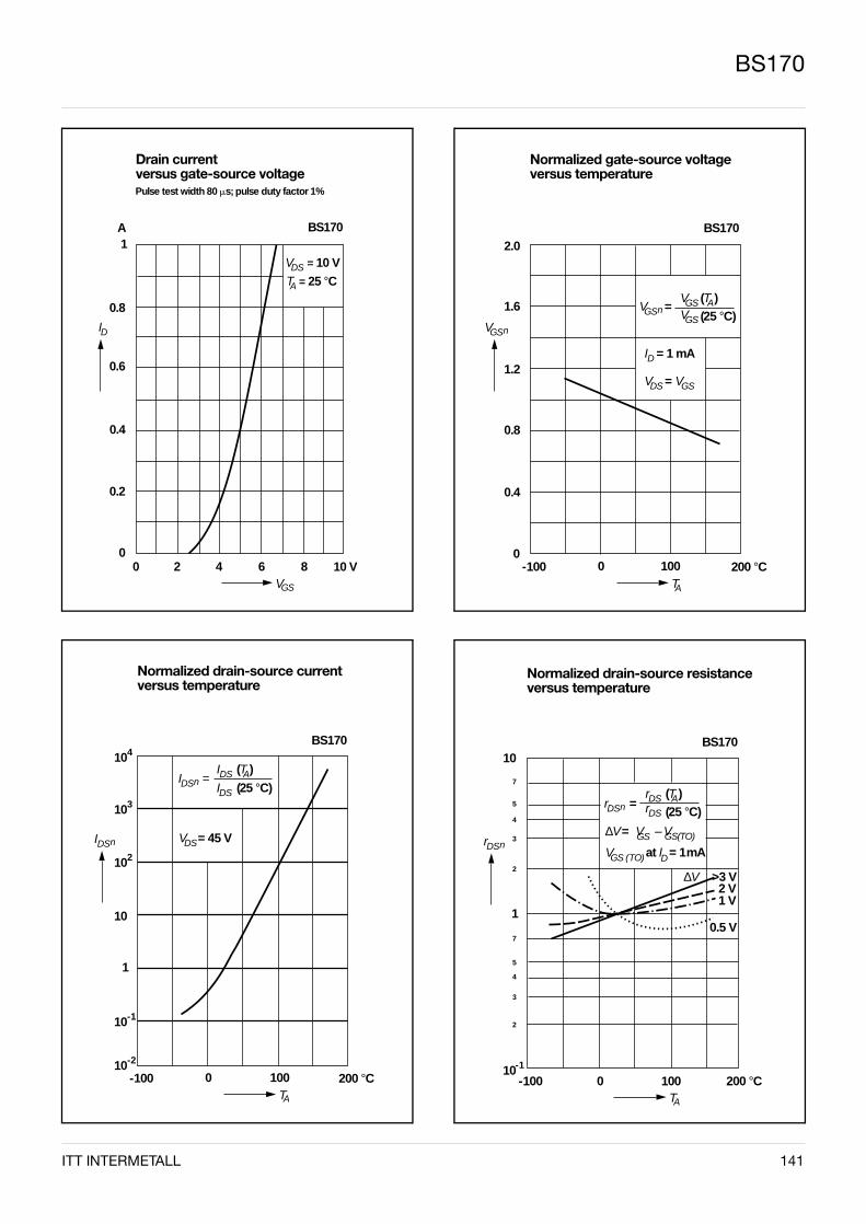
ITT INTERMETALL 141
Normalized drain-source resistance versus temperature
10
1
-100TA
200 °C
BS170
10-1
0
rDSn
7
5
4
3
2
7
5
4
3
2
100
rDS (T )A
(25 °C)r =DSn rDS
∆V = V – V GS
GS (TO)V at I = 1 mAD
>3 V2 V1 V
0.5 V
∆V
GS(TO)
Normalized drain-source current versus temperature
-100TA
200 °C
BS170104
103
102
10
1
10-2
0 100
IDSn
IDS (T )A
IDS (25 °C)
V = 45 VDS
10-1
I =DSn
Normalized gate-source voltage versus temperature
VGS
-100TA
200 °C
BS1702.0
100
n
VGS (T )A
(25 °C)
I = 1 mAD
1.6
1.2
0.8
0.4
00
V =GSn VGS
V = DS VGS
Drain current versus gate-source voltage
A1
ID
0.6
0.4
00
0.2
VGS
10 V
Pulse test width 80 ms; pulse duty factor 1%
BS170
0.8
2 4 6 8
V = 10 VDS
T = 25 °CA
BS170
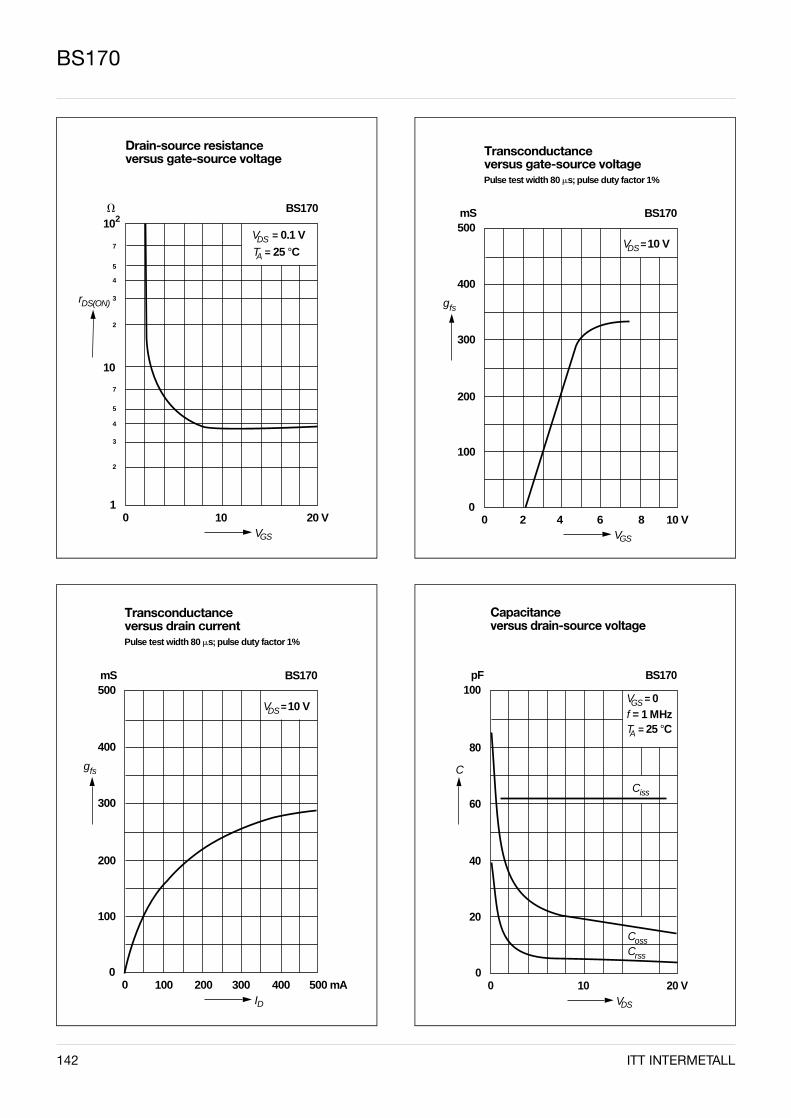
142 ITT INTERMETALL
Capacitance versus drain-source voltage
pF100
C
1000
VDS
20 V
BS170
80
60
40
20
V = 0GSf = 1 MHzT = 25 °CA
Ciss
CossCrss
Transconductance versus drain current
mS500
gfs
00
ID
500 mA
Pulse test width 80 ms; pulse duty factor 1%
BS170
400
300
200
100
100 200 300 400
V = 10 VDS
Drain-source resistance versus gate-source voltage
V
rDS(ON)
1001
VGS
20 V
BS170102
7
5
4
3
2
10
7
5
4
3
2
V = 0.1 VDS
T = 25 °CA
Transconductance versus gate-source voltage
mS500
gfs
00
VGS
10 V
Pulse test width 80 ms; pulse duty factor 1%
BS170
400
300
200
100
2 4 6 8
V = 10 VDS
BS170

ITT INTERMETALL 143
BS170

BS809
Absolute Maximum Ratings
Symbol Value Unit
Drain-Source Voltage VDSS 400 V
Drain-Gate Voltage VDGS 400 V
Gate-Source Voltage (pulsed) VGS ±20 V
Drain Current (continuous) at TSB = 50 °C ID 100 mA
Power Dissipation at TSB = 50 °C Ptot 3101) mW
Junction Temperature Tj 150 °C
Storage Temperature Range TS –65 to +150 °C
1) Device on fiberglass substrate, see layout
Inverse Diode
Symbol Value Unit
Max. Forward Current (continuous)at Tamb = 25 °C
IF 300 mA
Forward Voltage Drop (typ.)at VGS = 0 V, IF = 300 mA, Tj = 25 °C
VF 1.0 V
N-Channel Enhancement Mode DMOS Transistor
Features– high input impedance– low gate threshold voltage– low drain-source ON resistance– high-speed switching– no minority carrier storage time– CMOS logic compatible input– no thermal runaway– no secondary breakdown
Pin Configuration1 = Drain, 2 = Gate, 3 = Source
MarkingS09
144
0.4
0.95 0.95
3
0.4 0.4
+0.1
1
2 3
Top View
SOT-23 Plastic PackageWeight approx. 0.008 gDimensions in mm
2.45+0.1
ITT INTERMETALL
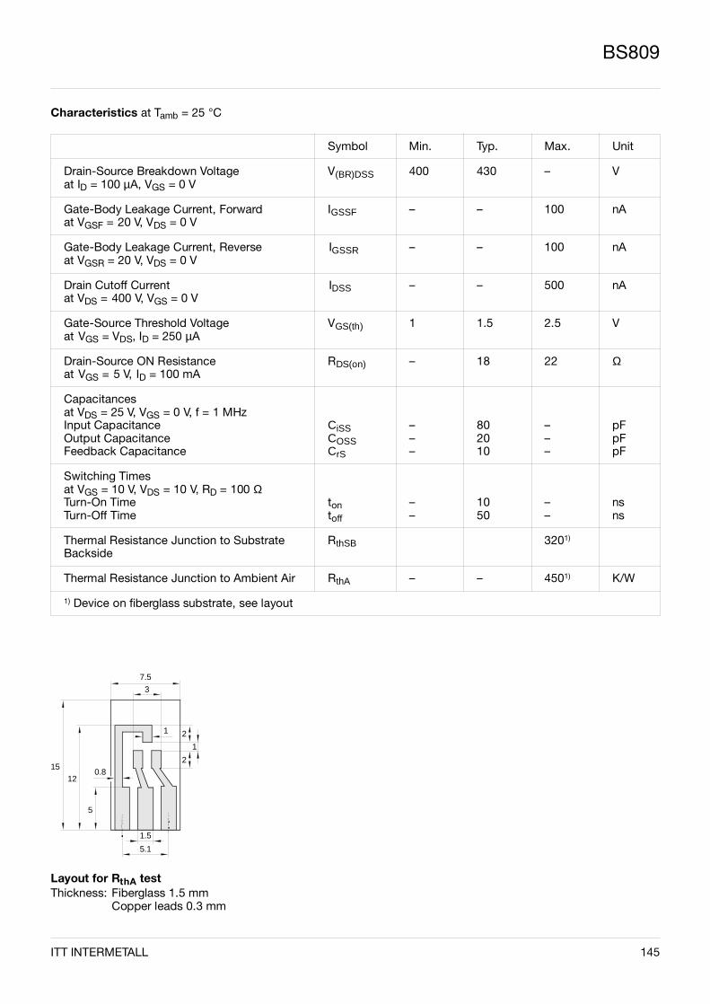
BS809
Characteristics at Tamb = 25 °C
Symbol Min. Typ. Max. Unit
Drain-Source Breakdown Voltageat ID = 100 µA, VGS = 0 V
V(BR)DSS 400 430 – V
Gate-Body Leakage Current, Forwardat VGSF = 20 V, VDS = 0 V
IGSSF – – 100 nA
Gate-Body Leakage Current, Reverseat VGSR = 20 V, VDS = 0 V
IGSSR – – 100 nA
Drain Cutoff Currentat VDS = 400 V, VGS = 0 V
IDSS – – 500 nA
Gate-Source Threshold Voltageat VGS = VDS, ID = 250 µA
VGS(th) 1 1.5 2.5 V
Drain-Source ON Resistanceat VGS = 5 V, ID = 100 mA
RDS(on) – 18 22 Ω
Capacitancesat VDS = 25 V, VGS = 0 V, f = 1 MHzInput CapacitanceOutput CapacitanceFeedback Capacitance
CiSSCOSSCrS
–––
802010
–––
pFpFpF
Switching Timesat VGS = 10 V, VDS = 10 V, RD = 100 ΩTurn-On TimeTurn-Off Time
tontoff
––
1050
––
nsns
Thermal Resistance Junction to SubstrateBackside
RthSB 3201)
Thermal Resistance Junction to Ambient Air RthA – – 4501) K/W
1) Device on fiberglass substrate, see layout
Layout for RthA testThickness: Fiberglass 1.5 mm
Copper leads 0.3 mm
15 12
5
0.8
7.5
3
1
1.5
5.1
2
2
1
ITT INTERMETALL 145

BS828
N-Channel Enhancement Mode DMOS Transistor
Features– high breakdown voltage– high input impedance– high-speed switching– no minority carrier storage time– CMOS logic compatible input– no thermal runaway– no secondary breakdown– specially suited for telephone subsets
Pin configuration1 = Drain, 2 = Gate, 3 = Source.
MarkingS28
0.4
0.95 0.95
3
0.4 0.4
+0.1
1
2 3
Top View
SOT-23 Plastic PackageWeight approx. 0.008 gDimensions in mm
2.45+0.1
Absolute Maximum Ratings
Inverse Diode
Symbol Value Unit
Drain-Source Voltage VDSS 240 V
Drain-Gate Voltage VDGS 240 V
Gate-Source Voltage (pulsed) VGS ± 20 V
Drain Current (continuous) ID 230 mA
Power Dissipation at TSB = 50 °C Ptot 0.3101) W
Junction Temperature Tj 150 °C
Storage Temperature Range TS –65…+150 °C
1) Device on fiberglass substrate, see layout
Symbol Value Unit
Max. Forward Current (continuous)at Tamb = 25 °C
IF 0.3 A
Forward Voltage Drop (typ.)at VGS = 0, IF = 0.3 A, Tj = 25 °C
VF 0.85 V
146 ITT INTERMETALL
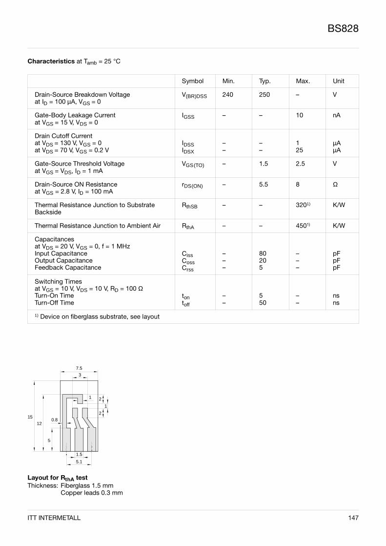
BS828
Characteristics at Tamb = 25 °C
Symbol Min. Typ. Max. Unit
Drain-Source Breakdown Voltageat ID = 100 µA, VGS = 0
V(BR)DSS 240 250 – V
Gate-Body Leakage Currentat VGS = 15 V, VDS = 0
IGSS – – 10 nA
Drain Cutoff Currentat VDS = 130 V, VGS = 0at VDS = 70 V, VGS = 0.2 V
IDSSIDSX
––
––
125
µAµA
Gate-Source Threshold Voltageat VGS = VDS, ID = 1 mA
VGS(TO) – 1.5 2.5 V
Drain-Source ON Resistanceat VGS = 2.8 V, ID = 100 mA
rDS(ON) – 5.5 8 Ω
Thermal Resistance Junction to SubstrateBackside
RthSB – – 3201) K/W
Thermal Resistance Junction to Ambient Air RthA – – 4501) K/W
Capacitancesat VDS = 20 V, VGS = 0, f = 1 MHzInput CapacitanceOutput CapacitanceFeedback Capacitance
CissCossCrss
–––
80205
–––
pFpFpF
Switching Timesat VGS = 10 V, VDS = 10 V, RD = 100 ΩTurn-On TimeTurn-Off Time
tontoff
––
550
––
nsns
1) Device on fiberglass substrate, see layout
ITT INTERMETALL 147
Layout for RthA testThickness: Fiberglass 1.5 mm
Copper leads 0.3 mm
15 12
5
0.8
7.5
3
1
1.5
5.1
2
2
1
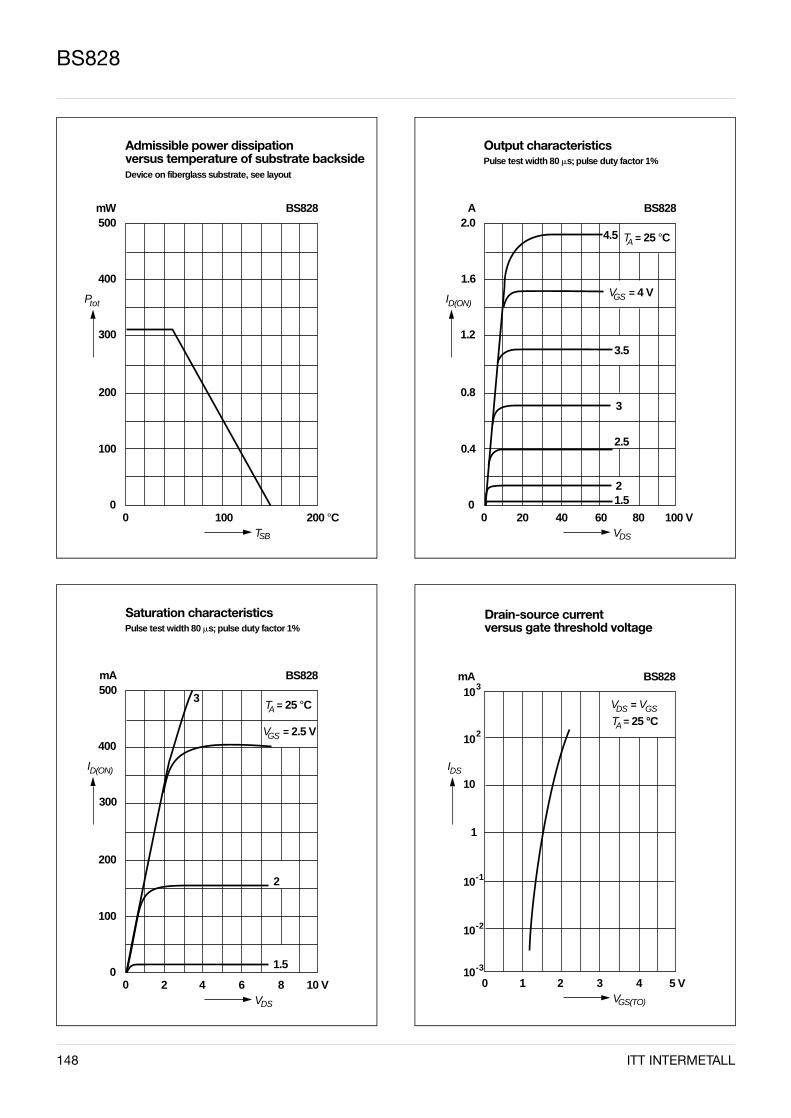
148 ITT INTERMETALL
BS828
Admissible power dissipation versus temperature of substrate backside
mW500
Ptot
300
200
10000
100
TSB
200 °C
Device on fiberglass substrate, see layout
BS828
400
Saturation characteristics
mA500
ID(ON)
300
200
600
100
VDS
10 V
Pulse test width 80 ms; pulse duty factor 1%
BS828
400
T = 25 °CA
V = 2.5 VGS
2 4 8
1.5
2
3
Output characteristics
A2.0
ID(ON)
1.2
0.8
6000
0.4
VDS
100 V
Pulse test width 80 ms; pulse duty factor 1%
BS828
1.6
T = 25 °CA
V = 4 VGS
20 40 80
3
3.5
2
4.5
2.5
1.5
Drain-source current versus gate threshold voltage
mA
0VGS(TO)
5 V
BS828
10
1
10-1
103
102
10-2
10-3
1 2 3 4
IDS
V = VDS GS
T = 25 °CA
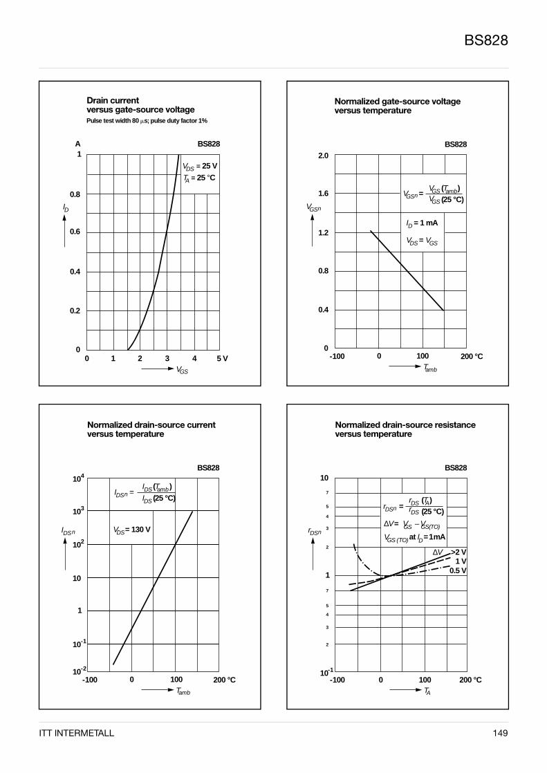
ITT INTERMETALL 149
BS828
Drain current versus gate-source voltage
A1
ID
0.6
0.4
00
0.2
VGS
5 V
Pulse test width 80 ms; pulse duty factor 1%
BS828
0.8
1 2 3 4
V = 25 VDS
T = 25 °CA
Normalized drain-source current versus temperature
-100Tamb
200 °C
BS828104
103
102
10
1
10-2
0 100
IDSn
IDS (T )amb
IDS (25 °C)
V = 130 VDS
10-1
I =DSn
Normalized gate-source voltage versus temperature
VGS
-100Tamb
200 °C
BS8282.0
100
n
VGS (T )amb
(25 °C)
I = 1 mAD
1.6
1.2
0.8
0.4
00
V =GSn VGS
V = DS VGS
Normalized drain-source resistance versus temperature
10
1
-100TA
200 °C
BS828
10-1
0
rDSn
7
5
4
3
2
7
5
4
3
2
100
rDS (T )A
(25 °C)r =DSn rDS
∆V = V – V GS
GS (TO)V at I = 1 mAD
>2 V1 V
0.5 V
∆V
GS(TO)
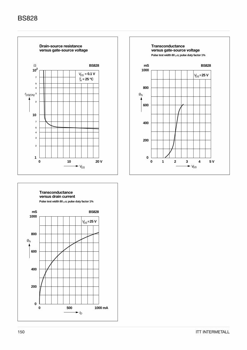
150 ITT INTERMETALL
BS828
Drain-source resistance versus gate-source voltage
V
rDS(ON)
1001
VGS
20 V
BS828102
7
5
4
3
2
10
7
5
4
3
2
V = 0.1 VDS
T = 25 °CA
Transconductance versus gate-source voltage
mS1000
gfs
00
VGS
Pulse test width 80 ms; pulse duty factor 1%
BS828
800
600
400
200
V = 25 VDS
1 2 3 4 5 V
Transconductance versus drain current
mS1000
gfs
00
ID
1000 mA
Pulse test width 80 ms; pulse duty factor 1%
BS828
800
600
400
200
500
V = 25 VDS

BS828
ITT INTERMETALL 151

BS870
N-Channel Enhancement Mode DMOS Transistor
Features– high input impedance– high-speed switching– no minority carrier storage time– CMOS logic compatible input– no thermal runaway– no secondary breakdown
Pin configuration1 = Drain, 2 = Gate, 3 = Source.
Marking S70
0.4
0.95 0.95
3
0.4 0.4
+0.1
1
2 3
Top View
SOT-23 Plastic PackageWeight approx. 0.008 gDimensions in mm
2.45+0.1
Absolute Maximum Ratings
Inverse Diode
Symbol Value Unit
Drain-Source Voltage VDSS 60 V
Drain-Gate Voltage VDGS 60 V
Gate-Source Voltage (pulsed) VGS ± 20 V
Drain Current (continuous) ID 250 mA
Power Dissipation at TSB = 50 °C Ptot 0.3101) W
Junction Temperature Tj 150 °C
Storage Temperature Range TS –65…+150 °C
1) Device on fiberglass substrate, see layout
Symbol Value Unit
Max. Forward Current (continuous)at Tamb = 25 °C
IF 0.3 A
Forward Voltage Drop (typ.)at VGS = 0, IF = 0.3 A, Tj = 25 °C
VF 0.85 V
152 ITT INTERMETALL
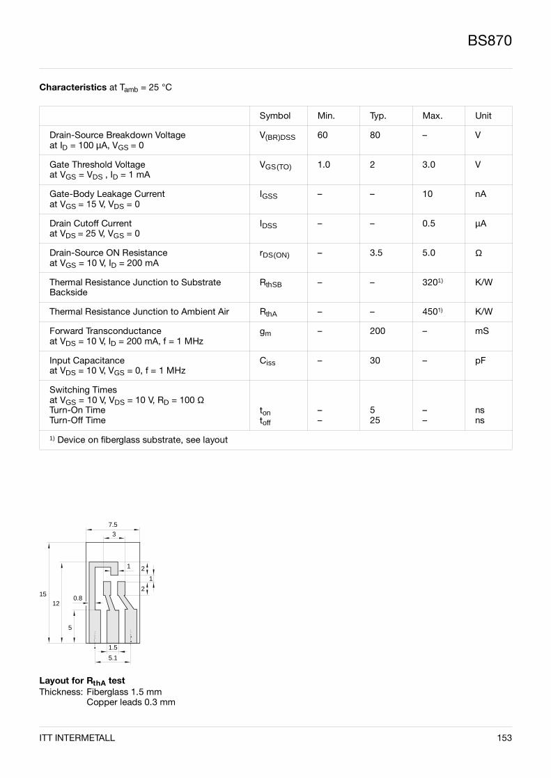
BS870
Characteristics at Tamb = 25 °C
Symbol Min. Typ. Max. Unit
Drain-Source Breakdown Voltageat ID = 100 µA, VGS = 0
V(BR)DSS 60 80 – V
Gate Threshold Voltageat VGS = VDS , ID = 1 mA
VGS(TO) 1.0 2 3.0 V
Gate-Body Leakage Currentat VGS = 15 V, VDS = 0
IGSS – – 10 nA
Drain Cutoff Current at VDS = 25 V, VGS = 0
IDSS – – 0.5 µA
Drain-Source ON Resistanceat VGS = 10 V, ID = 200 mA
rDS(ON) – 3.5 5.0 Ω
Thermal Resistance Junction to SubstrateBackside
RthSB – – 3201) K/W
Thermal Resistance Junction to Ambient Air RthA – – 4501) K/W
Forward Transconductanceat VDS = 10 V, ID = 200 mA, f = 1 MHz
gm – 200 – mS
Input Capacitanceat VDS = 10 V, VGS = 0, f = 1 MHz
Ciss – 30 – pF
Switching Timesat VGS = 10 V, VDS = 10 V, RD = 100 ΩTurn-On TimeTurn-Off Time
tontoff
––
525
––
nsns
1) Device on fiberglass substrate, see layout
Layout for RthA testThickness: Fiberglass 1.5 mm
Copper leads 0.3 mm
15 12
5
0.8
7.5
3
1
1.5
5.1
2
2
1
ITT INTERMETALL 153
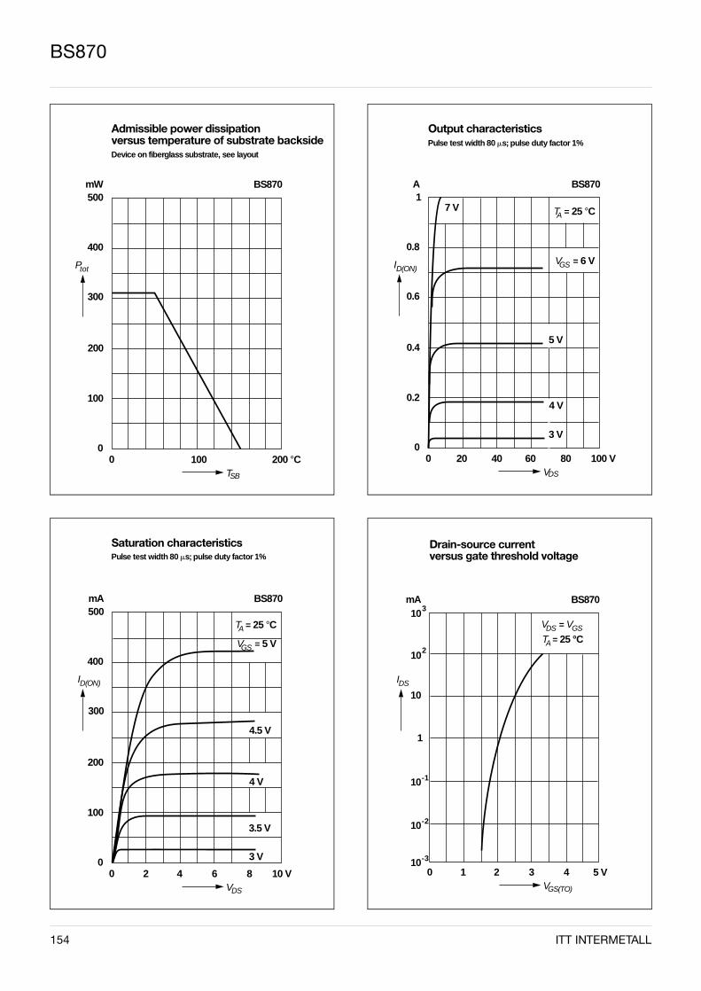
154 ITT INTERMETALL
BS870
Admissible power dissipation versus temperature of substrate backside
mW500
Ptot
300
200
10000
100
TSB
200 °C
Device on fiberglass substrate, see layout
BS870
400
Saturation characteristics
mA500
ID(ON)
300
200
600
100
VDS
10 V
Pulse test width 80 ms; pulse duty factor 1%
BS870
400
T = 25 °CA
V = 5 VGS
2 4 8
3 V
3.5 V
4 V
4.5 V
Output characteristics
A1
0.6
0.4
4000
0.2
VDS
100 V
Pulse test width 80 ms; pulse duty factor 1%
BS870
0.8
20 60 80
ID(ON)
T = 25 °CA
V = 6 VGS
5 V
4 V
3 V
7 V
Drain-source current versus gate threshold voltage
mA
0VGS(TO)
5 V
BS870
10
1
10-1
103
102
10-2
10-3
1 2 3 4
IDS
V = VDS GS
T = 25 °CA
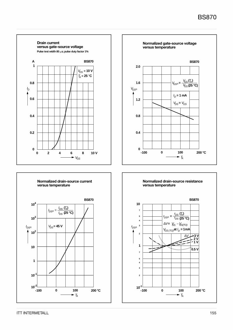
ITT INTERMETALL 155
BS870
Drain current versus gate-source voltage
A1
ID
0.6
0.4
00
0.2
VGS
10 V
Pulse test width 80 ms; pulse duty factor 1%
BS870
0.8
2 4 6 8
V = 10 VDS
T = 25 °CA
Normalized drain-source current versus temperature
-100TA
200 °C
BS870104
103
102
10
1
10-2
0 100
IDSn
IDS (T )A
IDS (25 °C)
V = 45 VDS
10-1
I =DSn
Normalized gate-source voltage versus temperature
VGS
-100TA
200 °C
BS8702.0
100
n
VGS (T )A
(25 °C)
I = 1 mAD
1.6
1.2
0.8
0.4
00
V =GSn VGS
V = DS VGS
Normalized drain-source resistance versus temperature
10
1
-100TA
200 °C
BS870
10-1
0
rDSn
7
5
4
3
2
7
5
4
3
2
100
rDS (T )A
(25 °C)r =DSn rDS
∆V = V – V GS
GS (TO)V at I = 1 mAD
>3 V2 V1 V
0.5 V
∆V
GS(TO)
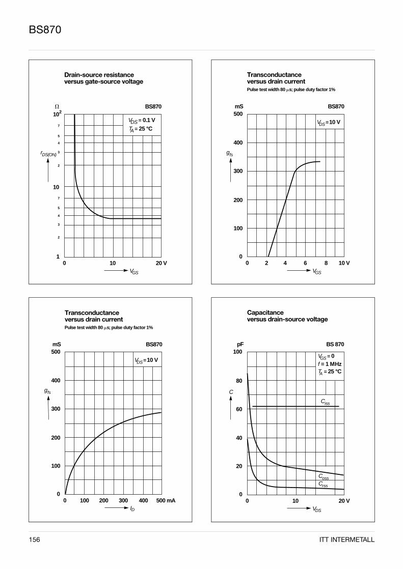
156 ITT INTERMETALL
BS870
Drain-source resistance versus gate-source voltage
V
rDS(ON)
1001
VGS
20 V
BS870102
7
5
4
3
2
10
7
5
4
3
2
V = 0.1 VDST = 25 °CA
Transconductance versus drain current
mS500
gfs
00
ID
500 mA
Pulse test width 80 ms; pulse duty factor 1%
BS870
400
300
200
100
100 200 300 400
V = 10 VDS
Transconductance versus drain current
mS500
gfs
00
VGS
10 V
Pulse test width 80 ms; pulse duty factor 1%
BS870
400
300
200
100
2 4 6 8
V = 10 VDS
Capacitance versus drain-source voltage
pF100
C
1000
VDS
20 V
BS 870
80
60
40
20
V = 0GSf = 1 MHzT = 25 °CA
Ciss
CossCrss

ITT INTERMETALL 157
BS870

158 ITT INTERMETALL
DMOS Transistors (P-Channel)
ITT INTERMETALL 159
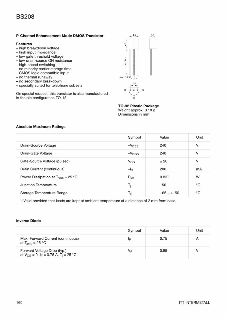
BS208
P-Channel Enhancement Mode DMOS Transistor
Features– high breakdown voltage– high input impedance– low gate threshold voltage– low drain-source ON resistance– high-speed switching– no minority carrier storage time– CMOS logic compatible input– no thermal runaway– no secondary breakdown– specially suited for telephone subsets
On special request, this transistor is also manufacturedin the pin configuration TO-18.
0.55∅ max.
2.5
G
SD
4.6 3.6
TO-92 Plastic PackageWeight approx. 0.18 gDimensions in mm
Absolute Maximum Ratings
Inverse Diode
Symbol Value Unit
Drain-Source Voltage –VDSS 240 V
Drain-Gate Voltage –VDGS 240 V
Gate-Source Voltage (pulsed) VGS ± 20 V
Drain Current (continuous) –ID 200 mA
Power Dissipation at Tamb = 25 °C Ptot 0.831) W
Junction Temperature Tj 150 °C
Storage Temperature Range TS –65…+150 °C
1) Valid provided that leads are kept at ambient temperature at a distance of 2 mm from case.
Symbol Value Unit
Max. Forward Current (continuous)at Tamb = 25 °C
IF 0.75 A
Forward Voltage Drop (typ.)at VGS = 0, IF = 0.75 A, Tj = 25 °C
VF 0.85 V
160 ITT INTERMETALL
BS208
Characteristics at Tamb = 25 °C
Symbol Min. Typ. Max. Unit
Drain-Source Breakdown Voltageat –ID = 100 µA, VGS = 0
–V(BR)DSS 240 250 – V
Gate-Body Leakage Currentat –VGS = 15 V, VDS = 0
–IGSS – – 10 nA
Drain Cutoff Currentat –VDS = 130 V, VGS = 0at –VDS = 70 V, –VGS = 0.2 V
–IDSS–IDSX
––
––
125
µAµA
Gate-Source Threshold Voltageat VGS = VDS, –ID = 1 mA
–VGS(TO) 0.8 1.5 2.5 V
Drain-Source ON Resistanceat –VGS = 5 V, –ID = 100 mA
rDS(ON) – 7 14 Ω
Thermal Resistance Junction to Ambient Air RthA – – 1501) K/W
Capacitancesat –VDS = 20 V, VGS = 0, f = 1 MHzInput CapacitanceOutput CapacitanceFeedback Capacitance
CissCossCrss
–––
2003010
–––
pFpFpF
Switching Times at –ID = 200 mA, –UGS = 10 VTurn-on TimeFall Time
tontf
––
515
––
nsns
1) Valid provided that leads are kept at ambient temperature at a distance of 2 mm from case.
ITT INTERMETALL 161
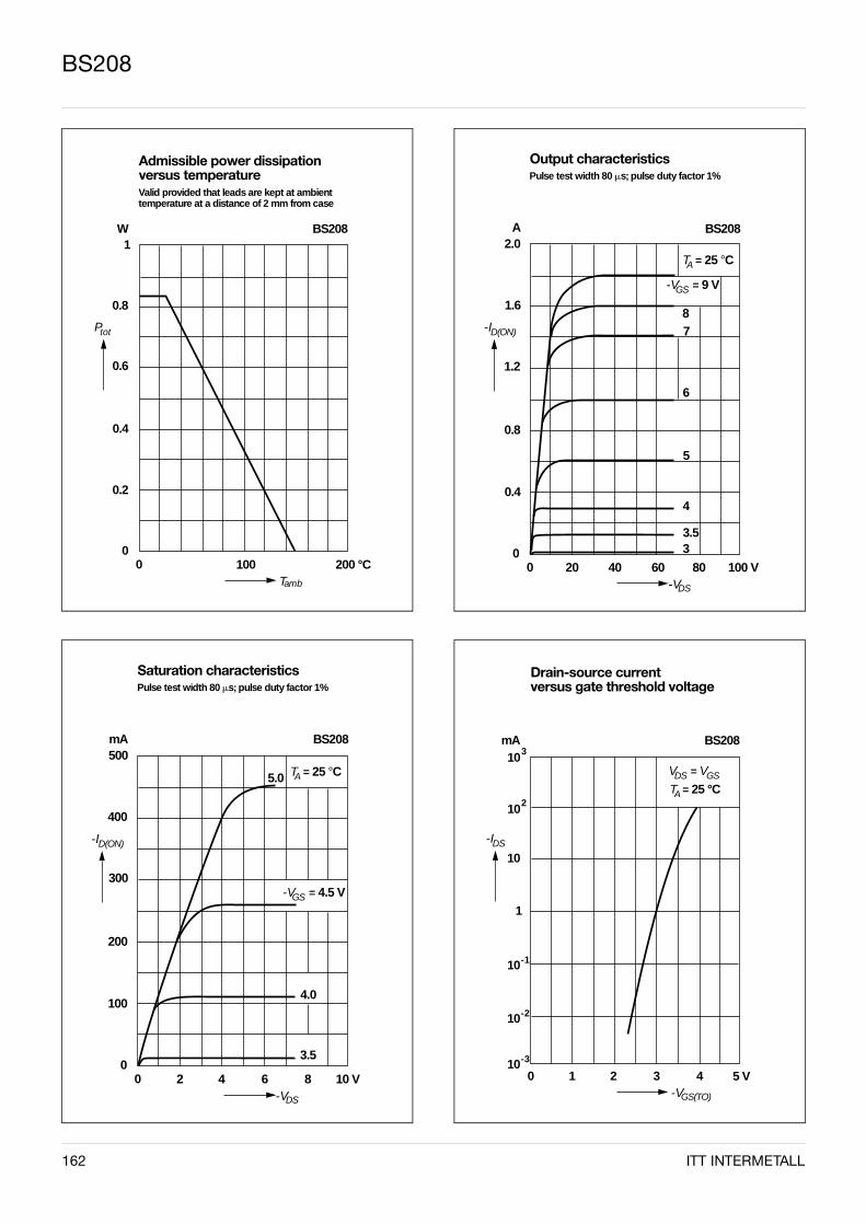
162 ITT INTERMETALL
BS208
Output characteristics
A2.0
-ID(ON)
1.2
0.8
6000
0.4
-VDS
100 V
Pulse test width 80 ms; pulse duty factor 1%
BS208
1.6
T = 25 °CA
-V = 9 VGS
20 40 80
5
6
3.5
4
3
87
Admissible power dissipation versus temperature
W1
Ptot
0.6
0.4
10000
0.2
Tamb
200 °C
Valid provided that leads are kept at ambient temperature at a distance of 2 mm from case
BS208
0.8
Saturation characteristics
mA500
-ID(ON)
300
200
600
100
-VDS
10 V
Pulse test width 80 ms; pulse duty factor 1%
BS208
400
T = 25 °CA
-V = 4.5 VGS
2 4 8
3.5
4.0
5.0
Drain-source current versus gate threshold voltage
mA
0-VGS(TO)
5 V
BS208
10
1
10-1
103
102
10-2
10-3
1 2 3 4
-IDS
V = VDS GS
T = 25 °CA
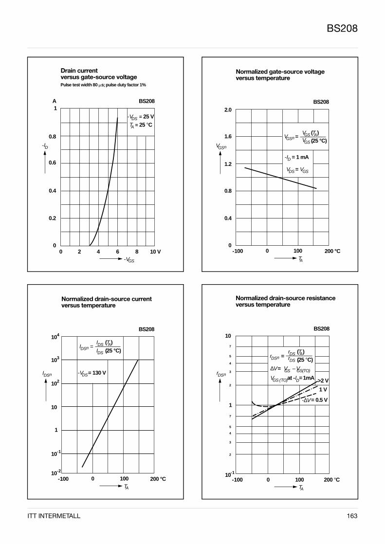
ITT INTERMETALL 163
BS208
Normalized gate-source voltage versus temperature
VGS
-100TA
200 °C
BS2082.0
100
n
VGS (T )A
(25 °C)
-I = 1 mAD
1.6
1.2
0.8
0.4
00
V =GSn VGS
V = DS VGS
Normalized drain-source current versus temperature
-100TA
200 °C
BS208104
103
102
10
1
10-2
0 100
IDSn
IDS (T )A
IDS (25 °C)
-V = 130 VDS
10-1
I =DSn
Drain current versus gate-source voltage
A1
-ID
0.6
0.4
00
0.2
-VGS
10 V
Pulse test width 80 ms; pulse duty factor 1%
BS208
0.8
2 4 6 8
-V = 25 VDS
T = 25 °CA
Normalized drain-source resistance versus temperature
10
1
-100TA
200 °C
BS208
10-1
0
rDSn
7
5
4
3
2
7
5
4
3
2
100
rDS (T )A
(25 °C)r =DSn rDS
∆V = V – V GS
GS (TO)V at -I = 1mAD >2 V
1 V
= 0.5 V-∆V
GS(TO)
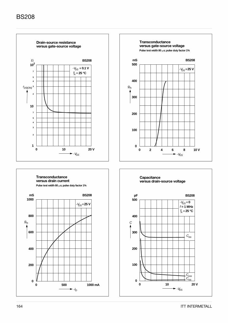
164 ITT INTERMETALL
BS208
Transconductance versus gate-source voltage
mS500
gfs
00
-VGS
Pulse test width 80 ms; pulse duty factor 1%
BS208
400
300
200
100
-V = 25 VDS
2 4 6 8 10 V
Transconductance versus drain current
mS1000
gfs
00
-ID
1000 mA
Pulse test width 80 ms; pulse duty factor 1%
BS208
800
600
400
200
500
-V = 25 VDS
Capacitance versus drain-source voltage
pF500
C
1000
-VDS
20 V
BS208
400
300
200
100
-V = 0GSf = 1 MHzT = 25 °CA
CossCrss
Ciss
Drain-source resistance versus gate-source voltage
V
rDS(ON)
1001
-VGS
20 V
BS208102
7
5
4
3
2
10
7
5
4
3
2
-V = 0.1 VDS
T = 25 °CA

ITT INTERMETALL 165
BS208

BS209
P-Channel Enhancement Mode DMOS Transistor
Features– high input impedance– low gate threshold voltage– low drain-source ON resistance– high-speed switching– no minority carrier storage time– CMOS logic compatible input– no thermal runaway– no secondary breakdown 0.55∅ max.
2.5
G
SD
4.6 3.6
TO-92 Plastic PackageWeight approx. 0.18 gDimensions in mm
Absolute Maximum Ratings
Symbol Value Unit
Drain-Source Voltage –VDSS 400 V
Drain-Gate Voltage –VDGS 400 V
Gate-Source Voltage (pulsed) VGS ±20 V
Drain Current (continuous) at Tamb = 25 °C –ID 120 mA
Power Dissipation at Tamb = 25 °C Ptot 8301) mW
Junction Temperature Tj 150 °C
Storage Temperature Range TS –65 to +150 °C
1) Valid provided that leads are kept at ambient temperature at a distance of 2 mm from case.
Inverse Diode
Symbol Value Unit
Max. Forward Current (continuous)at Tamb = 25 °C
IF 400 mA
Forward Voltage Drop (typ.)at VGS = 0 V, IF = 400 mA, Tj = 25 °C
VF 1.0 V
166 ITT INTERMETALL

BS209
Characteristics at Tamb = 25 °C
Symbol Min. Typ. Max. Unit
Drain-Source Breakdown Voltageat –ID = 100 µA, VGS = 0 V
–V(BR)DSS 400 430 – V
Gate-Body Leakage Current, Forwardat –VGSF = 20 V, VDS = 0 V
–IGSSF – – 100 nA
Gate-Body Leakage Current, Reverseat –VGSR = 20 V, VDS = 0 V
–IGSSR – – 100 nA
Drain Cutoff Currentat –VDS = 400 V, VGS = 0 V
–IDSS – – 500 nA
Gate-Source Threshold Voltageat VGS = VDS, –ID = 250 µA
–VGS(th) 1 1.5 2.5 V
Drain-Source ON Resistanceat –VGS = 5 V, –ID = 120 mA
RDS(on) – 50 60 Ω
Capacitanceat –VDS = 25 V, VGS = 0, f = 1 MHzInput CapacitanceOutput CapacitanceFeedback Capacitance
CiSSCOSSCrSS
–––
2003010
–––
pFpFpF
Switching Timesat –VGS = 10 V, –VDS = 10 V, RD = 100 ΩTurn-On TimeTurn-Off Time
tontoff
––
1050
––
nsns
Thermal Resistance Junction to Ambient Air RthA – – 1501) K/W
1) Valid provided that leads are kept at ambient temperature at a distance of 2 mm from case.
ITT INTERMETALL 167

BS223
P-Channel Enhancement Mode DMOS Transistor
Features– high input impedance– low gate threshold voltage– low drain-source ON resistance– high-speed switching– no minority carrier storage time– CMOS logic compatible input– no thermal runaway– no secondary breakdown 0.55∅ max.
2.5
G
SD
4.6 3.6
TO-92 Plastic PackageWeight approx. 0.18 gDimensions in mm
Absolute Maximum Ratings
Symbol Value Unit
Drain-Source Voltage –VDSS 60 V
Drain-Gate Voltage –VDGS 60 V
Gate-Source Voltage (pulsed) VGS ±20 V
Drain Current (continuous) at Tamb = 25 °C –ID 1 A
Power Dissipation at Tamb = 25 °C Ptot 8301) mW
Junction Temperature Tj 150 °C
Storage Temperature Range TS –65 to +150 °C
1) Valid provided that leads are kept at ambient temperature at a distance of 2 mm from case.
Inverse Diode
Symbol Value Unit
Max. Forward Current (continuous)at Tamb = 25 °C
IF 1 A
Forward Voltage Drop (typ.)at VGS = 0 V, IF = 1 mA, Tj = 25 °C
VF 1.0 V
168 ITT INTERMETALL
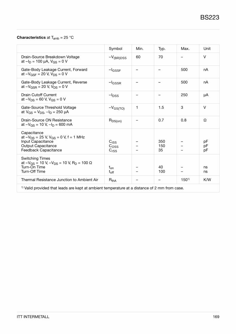
BS223
Characteristics at Tamb = 25 °C
Symbol Min. Typ. Max. Unit
Drain-Source Breakdown Voltageat –ID = 100 µA, VGS = 0 V
–V(BR)DSS 60 70 – V
Gate-Body Leakage Current, Forwardat –VGSF = 20 V, VDS = 0 V
–IGSSF – – 500 nA
Gate-Body Leakage Current, Reverseat –VGSR = 20 V, VDS = 0 V
–IGSSR – – 500 nA
Drain Cutoff Currentat –VDS = 60 V, VGS = 0 V
–IDSS – – 250 µA
Gate-Source Threshold Voltageat VGS = VDS, –ID = 250 µA
–VGS(TO) 1 1.5 3 V
Drain-Source ON Resistanceat –VGS = 10 V, –ID = 600 mA
RDS(on) – 0.7 0.8 Ω
Capacitanceat –VDS = 25 V, VGS = 0 V, f = 1 MHzInput CapacitanceOutput CapacitanceFeedback Capacitance
CiSSCOSSCrSS
–––
35015035
–––
pFpFpF
Switching Timesat –VGS = 10 V, –VDS = 10 V, RD = 100 ΩTurn-On TimeTurn-Off Time
tontoff
––
40100
––
nsns
Thermal Resistance Junction to Ambient Air RthA – – 1501) K/W
1) Valid provided that leads are kept at ambient temperature at a distance of 2 mm from case.
ITT INTERMETALL 169
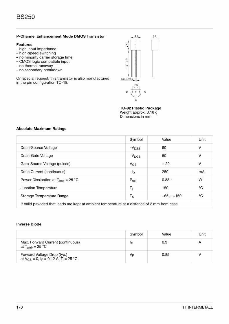
BS250
P-Channel Enhancement Mode DMOS Transistor
Features– high input impedance– high-speed switching– no minority carrier storage time– CMOS logic compatible input– no thermal runaway– no secondary breakdown
On special request, this transistor is also manufacturedin the pin configuration TO-18.
0.55∅ max.
2.5
G
SD
4.6 3.6
TO-92 Plastic PackageWeight approx. 0.18 gDimensions in mm
Absolute Maximum Ratings
Inverse Diode
Symbol Value Unit
Drain-Source Voltage –VDSS 60 V
Drain-Gate Voltage –VDGS 60 V
Gate-Source Voltage (pulsed) VGS ± 20 V
Drain Current (continuous) –ID 250 mA
Power Dissipation at Tamb = 25 °C Ptot 0.831) W
Junction Temperature Tj 150 °C
Storage Temperature Range TS –65…+150 °C
1) Valid provided that leads are kept at ambient temperature at a distance of 2 mm from case.
Symbol Value Unit
Max. Forward Current (continuous)at Tamb = 25 °C
IF 0.3 A
Forward Voltage Drop (typ.)at VGS = 0, IF = 0.12 A, Tj = 25 °C
VF 0.85 V
170 ITT INTERMETALL
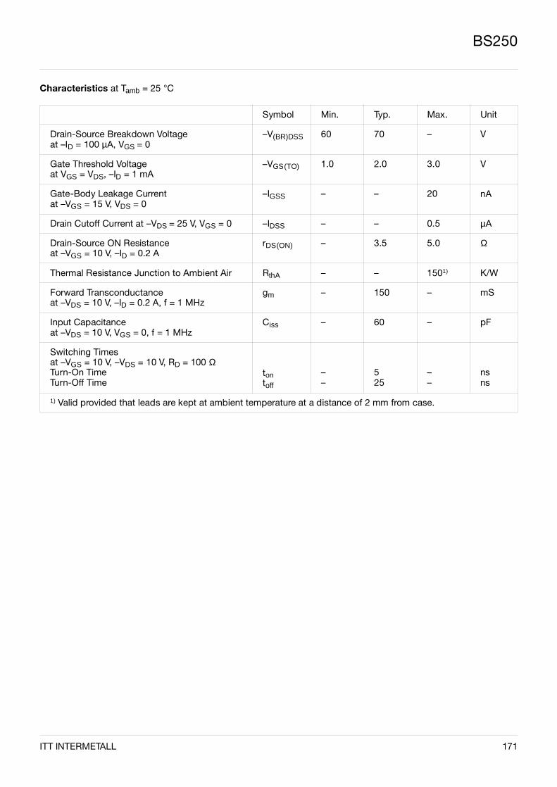
BS250
Characteristics at Tamb = 25 °C
Symbol Min. Typ. Max. Unit
Drain-Source Breakdown Voltageat –ID = 100 µA, VGS = 0
–V(BR)DSS 60 70 – V
Gate Threshold Voltageat VGS = VDS, –ID = 1 mA
–VGS(TO) 1.0 2.0 3.0 V
Gate-Body Leakage Currentat –VGS = 15 V, VDS = 0
–IGSS – – 20 nA
Drain Cutoff Current at –VDS = 25 V, VGS = 0 –IDSS – – 0.5 µA
Drain-Source ON Resistanceat –VGS = 10 V, –ID = 0.2 A
rDS(ON) – 3.5 5.0 Ω
Thermal Resistance Junction to Ambient Air RthA – – 1501) K/W
Forward Transconductanceat –VDS = 10 V, –ID = 0.2 A, f = 1 MHz
gm – 150 – mS
Input Capacitanceat –VDS = 10 V, VGS = 0, f = 1 MHz
Ciss – 60 – pF
Switching Timesat –VGS = 10 V, –VDS = 10 V, RD = 100 ΩTurn-On TimeTurn-Off Time
tontoff
––
525
––
nsns
1) Valid provided that leads are kept at ambient temperature at a distance of 2 mm from case.
ITT INTERMETALL 171
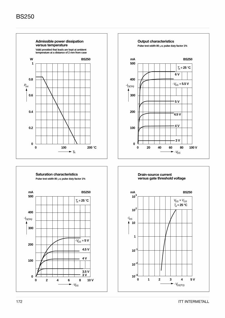
172 ITT INTERMETALL
BS250
Admissible power dissipation versus temperature
W1
Ptot
0.6
0.4
10000
0.2
TA
200 °C
Valid provided that leads are kept at ambient temperature at a distance of 2 mm from case
BS250
0.8
Output characteristics
mA500
-ID(ON)
300
200
6000
100
-VDS
100 V
Pulse test width 80 ms; pulse duty factor 1%
BS250
400
T = 25 °CA
-V = 5.5 VGS
20 40 80
6 V
4.5 V
5 V
3 V
4 V
Saturation characteristics
mA500
-ID(ON)
300
200
600
100
-VDS
10 V
Pulse test width 80 ms; pulse duty factor 1%
BS250
400
T = 25 °CA
-V = 5 VGS
2 4 8
3 V3.5 V
4 V
4.5 V
Drain-source current versus gate threshold voltage
mA
0-VGS(TO)
5 V
BS250
10
1
10-1
103
102
10-2
10-3
1 2 3 4
-IDS
V = VDS GS
T = 25 °CA
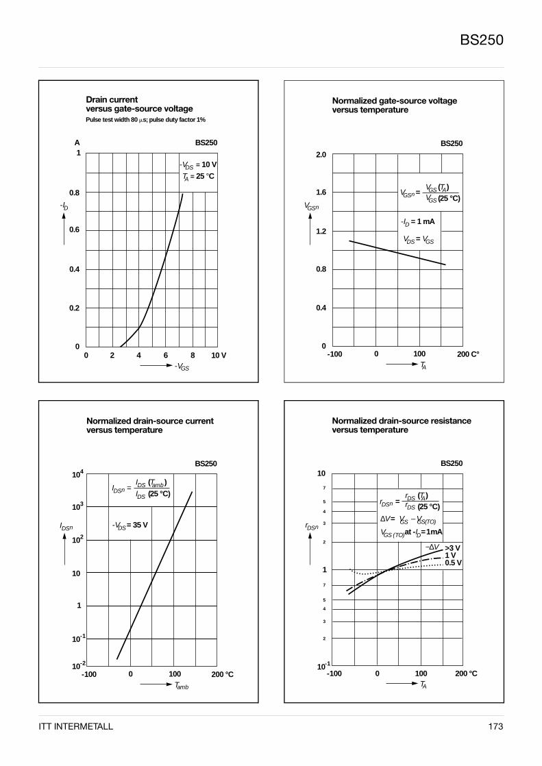
ITT INTERMETALL 173
BS250
Drain current versus gate-source voltage
A1
-ID
0.6
0.4
00
0.2
-VGS
10 V
Pulse test width 80 ms; pulse duty factor 1%
BS250
0.8
2 4 6 8
-V = 10 VDS
T = 25 °CA
Normalized drain-source current versus temperature
-100Tamb
200 °C
BS250104
103
102
10
1
10-2
0 100
IDSn
IDS (T )amb
IDS (25 °C)
-V = 35 VDS
10-1
I =DSn
Normalized drain-source resistance versus temperature
10
1
-100TA
200 °C
BS250
10-1
0
rDSn
7
5
4
3
2
7
5
4
3
2
100
rDS (T )A
(25 °C)r =DSn rDS
∆V = V – V GS
GS (TO)V at -I = 1 mAD
>3 V1 V0.5 V
−∆V
GS(TO)
Normalized gate-source voltage versus temperature
VGS
-100TA
200 C°
BS2502.0
100
n
VGS (T )A
(25 °C)
-I = 1 mAD
1.6
1.2
0.8
0.4
00
V =GSn VGS
V = DS VGS
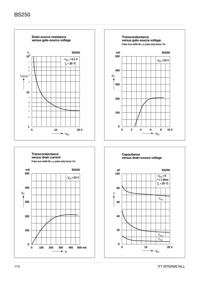
174 ITT INTERMETALL
BS250
Drain-source resistance versus gate-source voltage
V
rDS(ON)
1001
-VGS
20 V
BS250102
7
5
4
3
2
10
7
5
4
3
2
-V = 0.1 VDS
T = 25 °CA
Transconductance versus gate-source voltage
mS500
gfs
00
-VGS
10 V
Pulse test width 80 ms; pulse duty factor 1%
BS250
400
300
200
100
2 4 6 8
-V = 10 VDS
Transconductance versus drain current
mS500
gfs
00
-ID
500 mA
Pulse test width 80 ms; pulse duty factor 1%
BS250
400
300
200
100
100 200 300 400
-V = 10 VDS
Capacitance versus drain-source voltage
pF100
C
1000
-VDS
20 V
BS250
80
60
40
20
-V = 0GSf = 1 MHzT = 25 °CA
Ciss
Coss
Crss

ITT INTERMETALL 175
BS250
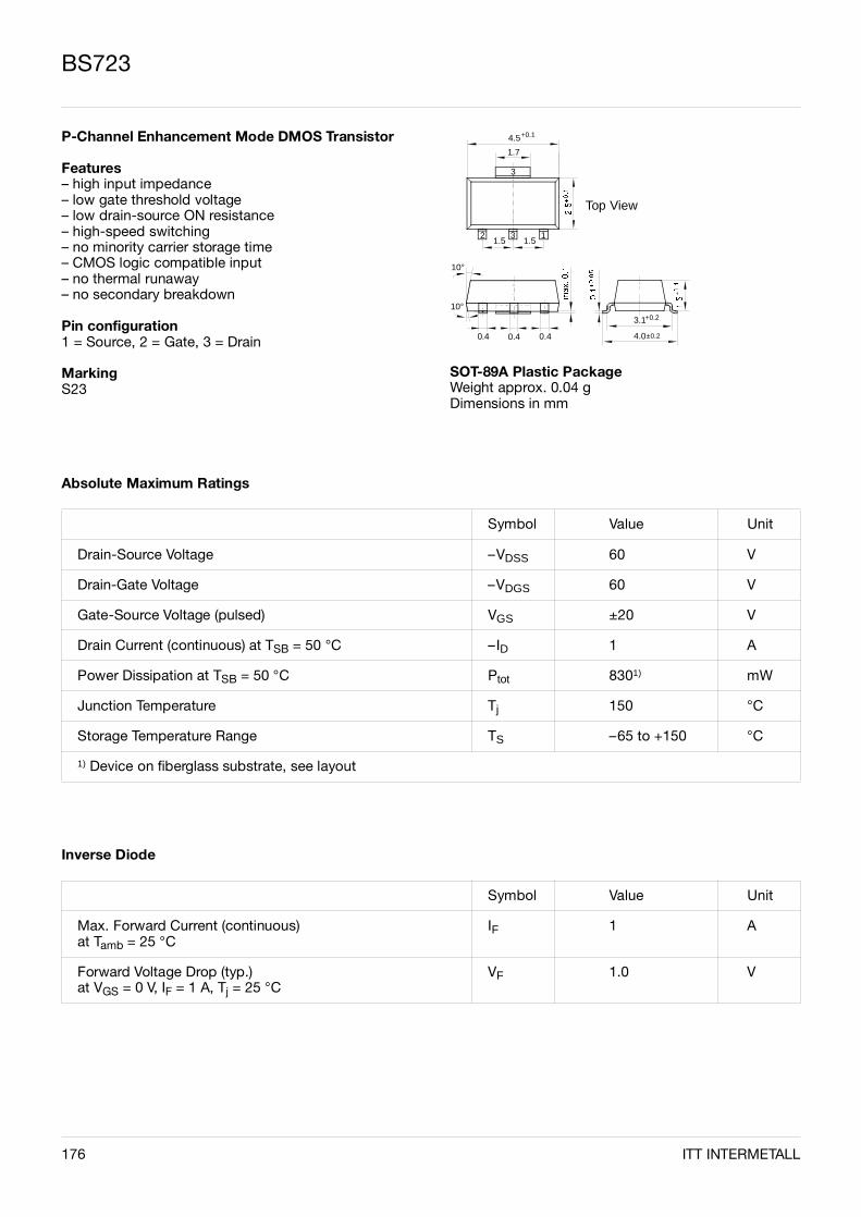
BS723
Absolute Maximum Ratings
Symbol Value Unit
Drain-Source Voltage –VDSS 60 V
Drain-Gate Voltage –VDGS 60 V
Gate-Source Voltage (pulsed) VGS ±20 V
Drain Current (continuous) at TSB = 50 °C –ID 1 A
Power Dissipation at TSB = 50 °C Ptot 8301) mW
Junction Temperature Tj 150 °C
Storage Temperature Range TS –65 to +150 °C
1) Device on fiberglass substrate, see layout
Inverse Diode
Symbol Value Unit
Max. Forward Current (continuous)at Tamb = 25 °C
IF 1 A
Forward Voltage Drop (typ.)at VGS = 0 V, IF = 1 A, Tj = 25 °C
VF 1.0 V
P-Channel Enhancement Mode DMOS Transistor
Features– high input impedance– low gate threshold voltage– low drain-source ON resistance– high-speed switching– no minority carrier storage time– CMOS logic compatible input– no thermal runaway– no secondary breakdown
Pin configuration1 = Source, 2 = Gate, 3 = Drain
MarkingS23
176
SOT-89A Plastic PackageWeight approx. 0.04 gDimensions in mm
1.7
4.5
1.5 1.5
10°
0.40.4 0.4 4.0
3.1
±0.2
+0.1
10°+0.2
3
2 3 1
Top View
ITT INTERMETALL
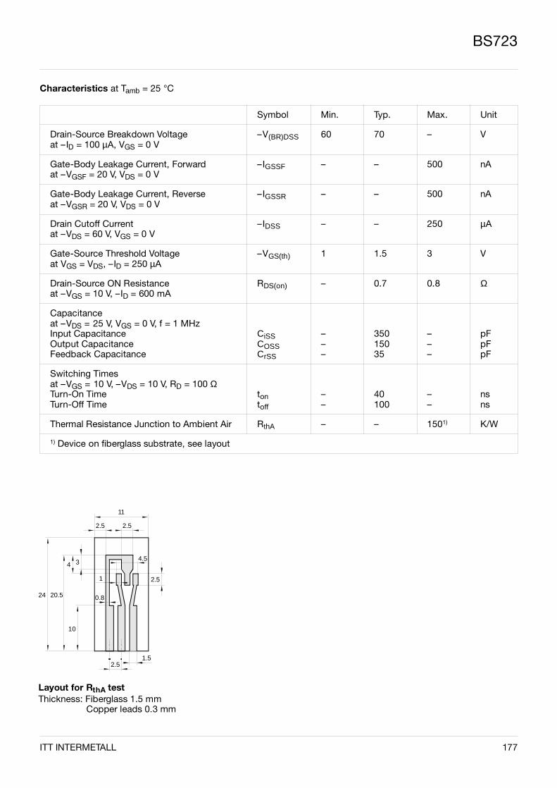
BS723
Characteristics at Tamb = 25 °C
Symbol Min. Typ. Max. Unit
Drain-Source Breakdown Voltageat –ID = 100 µA, VGS = 0 V
–V(BR)DSS 60 70 – V
Gate-Body Leakage Current, Forwardat –VGSF = 20 V, VDS = 0 V
–IGSSF – – 500 nA
Gate-Body Leakage Current, Reverseat –VGSR = 20 V, VDS = 0 V
–IGSSR – – 500 nA
Drain Cutoff Currentat –VDS = 60 V, VGS = 0 V
–IDSS – – 250 µA
Gate-Source Threshold Voltageat VGS = VDS, –ID = 250 µA
–VGS(th) 1 1.5 3 V
Drain-Source ON Resistanceat –VGS = 10 V, –ID = 600 mA
RDS(on) – 0.7 0.8 Ω
Capacitanceat –VDS = 25 V, VGS = 0 V, f = 1 MHzInput CapacitanceOutput CapacitanceFeedback Capacitance
CiSSCOSSCrSS
–––
35015035
–––
pFpFpF
Switching Timesat –VGS = 10 V, –VDS = 10 V, RD = 100 ΩTurn-On TimeTurn-Off Time
tontoff
––
40100
––
nsns
Thermal Resistance Junction to Ambient Air RthA – – 1501) K/W
1) Device on fiberglass substrate, see layout
Layout for RthA testThickness: Fiberglass 1.5 mm
Copper leads 0.3 mm
2.51.5
11
2.5 2.5
24 20.5
10
4 3
0.8
1
4.5
2.5
ITT INTERMETALL 177
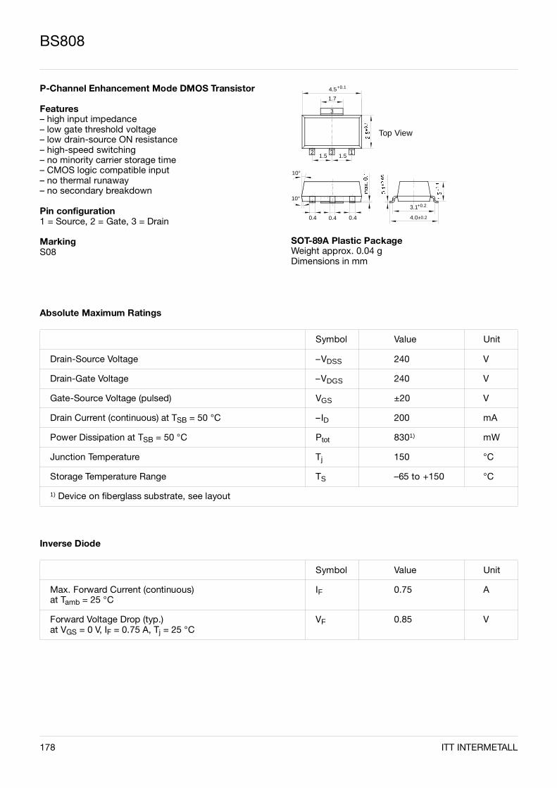
BS808
Absolute Maximum Ratings
Symbol Value Unit
Drain-Source Voltage –VDSS 240 V
Drain-Gate Voltage –VDGS 240 V
Gate-Source Voltage (pulsed) VGS ±20 V
Drain Current (continuous) at TSB = 50 °C –ID 200 mA
Power Dissipation at TSB = 50 °C Ptot 8301) mW
Junction Temperature Tj 150 °C
Storage Temperature Range TS –65 to +150 °C
1) Device on fiberglass substrate, see layout
Inverse Diode
Symbol Value Unit
Max. Forward Current (continuous)at Tamb = 25 °C
IF 0.75 A
Forward Voltage Drop (typ.)at VGS = 0 V, IF = 0.75 A, Tj = 25 °C
VF 0.85 V
P-Channel Enhancement Mode DMOS Transistor
Features– high input impedance– low gate threshold voltage– low drain-source ON resistance– high-speed switching– no minority carrier storage time– CMOS logic compatible input– no thermal runaway– no secondary breakdown
Pin configuration1 = Source, 2 = Gate, 3 = Drain
MarkingS08
178
SOT-89A Plastic PackageWeight approx. 0.04 gDimensions in mm
1.7
4.5
1.5 1.5
10°
0.40.4 0.4 4.0
3.1
±0.2
+0.1
10°+0.2
3
2 3 1
Top View
ITT INTERMETALL
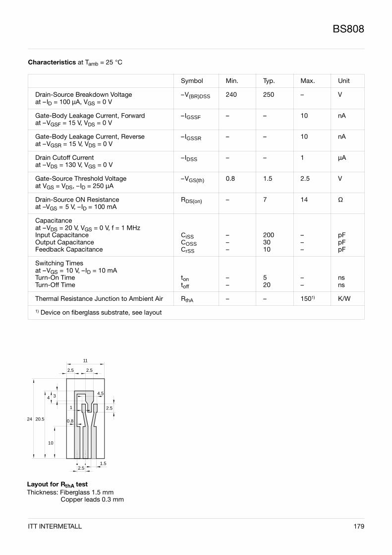
BS808
Characteristics at Tamb = 25 °C
Symbol Min. Typ. Max. Unit
Drain-Source Breakdown Voltageat –ID = 100 µA, VGS = 0 V
–V(BR)DSS 240 250 – V
Gate-Body Leakage Current, Forwardat –VGSF = 15 V, VDS = 0 V
–IGSSF – – 10 nA
Gate-Body Leakage Current, Reverseat –VGSR = 15 V, VDS = 0 V
–IGSSR – – 10 nA
Drain Cutoff Currentat –VDS = 130 V, VGS = 0 V
–IDSS – – 1 µA
Gate-Source Threshold Voltageat VGS = VDS, –ID = 250 µA
–VGS(th) 0.8 1.5 2.5 V
Drain-Source ON Resistanceat –VGS = 5 V, –ID = 100 mA
RDS(on) – 7 14 Ω
Capacitanceat –VDS = 20 V, VGS = 0 V, f = 1 MHzInput CapacitanceOutput CapacitanceFeedback Capacitance
CiSSCOSSCrSS
–––
2003010
–––
pFpFpF
Switching Timesat –VGS = 10 V, –ID = 10 mATurn-On TimeTurn-Off Time
tontoff
––
520
––
nsns
Thermal Resistance Junction to Ambient Air RthA – – 1501) K/W
1) Device on fiberglass substrate, see layout
Layout for RthA testThickness: Fiberglass 1.5 mm
Copper leads 0.3 mm
2.51.5
11
2.5 2.5
24 20.5
10
4 3
0.8
1
4.5
2.5
ITT INTERMETALL 179
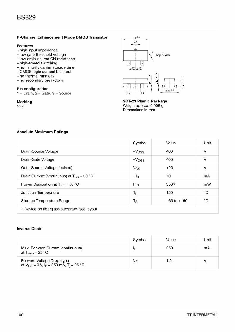
BS829
Absolute Maximum Ratings
Symbol Value Unit
Drain-Source Voltage –VDSS 400 V
Drain-Gate Voltage –VDGS 400 V
Gate-Source Voltage (pulsed) VGS ±20 V
Drain Current (continuous) at TSB = 50 °C – ID 70 mA
Power Dissipation at TSB = 50 °C Ptot 3501) mW
Junction Temperature Tj 150 °C
Storage Temperature Range TS –65 to +150 °C
1) Device on fiberglass substrate, see layout
Inverse Diode
Symbol Value Unit
Max. Forward Current (continuous)at Tamb = 25 °C
IF 350 mA
Forward Voltage Drop (typ.)at VGS = 0 V, IF = 350 mA, Tj = 25 °C
VF 1.0 V
P-Channel Enhancement Mode DMOS Transistor
Features– high input impedance– low gate threshold voltage– low drain-source ON resistance– high-speed switching– no minority carrier storage time– CMOS logic compatible input– no thermal runaway– no secondary breakdown
Pin configuration1 = Drain, 2 = Gate, 3 = Source
MarkingS29
180
0.4
0.95 0.95
3
0.4 0.4
+0.1
1
2 3
Top View
SOT-23 Plastic PackageWeight approx. 0.008 gDimensions in mm
2.45+0.1
ITT INTERMETALL
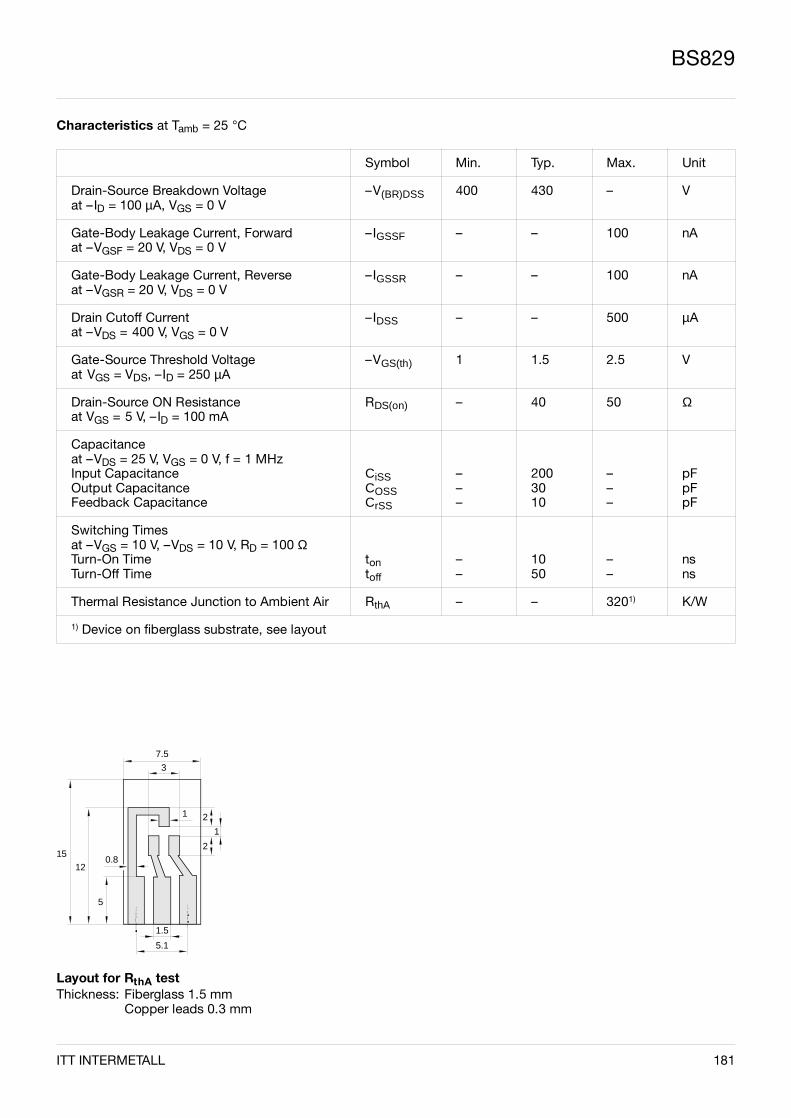
BS829
Characteristics at Tamb = 25 °C
Symbol Min. Typ. Max. Unit
Drain-Source Breakdown Voltageat –ID = 100 µA, VGS = 0 V
–V(BR)DSS 400 430 – V
Gate-Body Leakage Current, Forwardat –VGSF = 20 V, VDS = 0 V
–IGSSF – – 100 nA
Gate-Body Leakage Current, Reverseat –VGSR = 20 V, VDS = 0 V
–IGSSR – – 100 nA
Drain Cutoff Currentat –VDS = 400 V, VGS = 0 V
–IDSS – – 500 µA
Gate-Source Threshold Voltageat VGS = VDS, –ID = 250 µA
–VGS(th) 1 1.5 2.5 V
Drain-Source ON Resistanceat VGS = 5 V, –ID = 100 mA
RDS(on) – 40 50 Ω
Capacitanceat –VDS = 25 V, VGS = 0 V, f = 1 MHzInput CapacitanceOutput CapacitanceFeedback Capacitance
CiSSCOSSCrSS
–––
2003010
–––
pFpFpF
Switching Timesat –VGS = 10 V, –VDS = 10 V, RD = 100 ΩTurn-On TimeTurn-Off Time
tontoff
––
1050
––
nsns
Thermal Resistance Junction to Ambient Air RthA – – 3201) K/W
1) Device on fiberglass substrate, see layout
Layout for RthA testThickness: Fiberglass 1.5 mm
Copper leads 0.3 mm
15 12
5
0.8
7.5
3
1
1.5
5.1
2
2
1
ITT INTERMETALL 181

BS850
P-Channel Enhancement Mode DMOS Transistor
Features– high input impedance– high-speed switching– no minority carrier storage time– CMOS logic compatible input– no thermal runaway– no secondary breakdown
Pin configuration1 = Drain, 2 = Gate, 3 = Source
Marking S50
0.4
0.95 0.95
3
0.4 0.4
+0.1
1
2 3
Top View
SOT-23 Plastic PackageWeight approx. 0.008 gDimensions in mm
2.45+0.1
Absolute Maximum Ratings
Inverse Diode
Symbol Value Unit
Drain-Source Voltage –VDSS 60 V
Drain-Gate Voltage –VDGS 60 V
Gate-Source Voltage (pulsed) VGS ± 20 V
Drain Current (continuous) –ID 250 mA
Power Dissipation at TSB = 50 °C Ptot 0.3101) W
Junction Temperature Tj 150 °C
Storage Temperature Range TS –65…+150 °C
1) Device on fiberglass substrate, see layout
Symbol Value Unit
Max. Forward Current (continuous)at Tamb = 25 °C
IF 0.3 A
Forward Voltage Drop (typ.)at VGS = 0, IF = 0.12 A, Tj = 25 °C
VF 0.85 V
182 ITT INTERMETALL
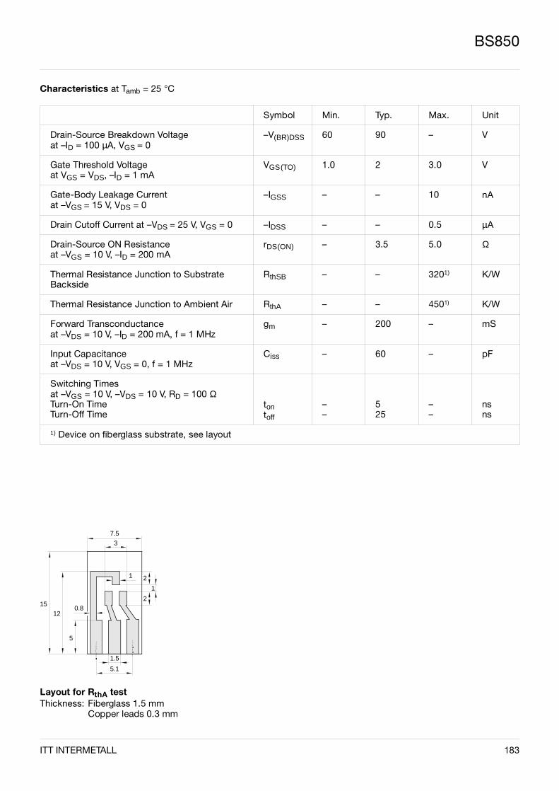
BS850
Characteristics at Tamb = 25 °C
Symbol Min. Typ. Max. Unit
Drain-Source Breakdown Voltageat –ID = 100 µA, VGS = 0
–V(BR)DSS 60 90 – V
Gate Threshold Voltageat VGS = VDS, –ID = 1 mA
VGS(TO) 1.0 2 3.0 V
Gate-Body Leakage Currentat –VGS = 15 V, VDS = 0
–IGSS – – 10 nA
Drain Cutoff Current at –VDS = 25 V, VGS = 0 –IDSS – – 0.5 µA
Drain-Source ON Resistanceat –VGS = 10 V, –ID = 200 mA
rDS(ON) – 3.5 5.0 Ω
Thermal Resistance Junction to SubstrateBackside
RthSB – – 3201) K/W
Thermal Resistance Junction to Ambient Air RthA – – 4501) K/W
Forward Transconductanceat –VDS = 10 V, –ID = 200 mA, f = 1 MHz
gm – 200 – mS
Input Capacitanceat –VDS = 10 V, VGS = 0, f = 1 MHz
Ciss – 60 – pF
Switching Timesat –VGS = 10 V, –VDS = 10 V, RD = 100 ΩTurn-On TimeTurn-Off Time
tontoff
––
525
––
nsns
1) Device on fiberglass substrate, see layout
Layout for RthA testThickness: Fiberglass 1.5 mm
Copper leads 0.3 mm
15 12
5
0.8
7.5
3
1
1.5
5.1
2
2
1
ITT INTERMETALL 183

184 ITT INTERMETALL
BS850
Admissible power dissipation versus temperature of substrate backside
mW500
Ptot
300
200
10000
100
TSB
200 °C
Device on fiberglass substrate, see layout
BS850
400
Saturation characteristics
mA500
-ID(ON)
300
200
600
100
-VDS
10 V
Pulse test width 80 ms; pulse duty factor 1%
BS850
400
T = 25 °CA
-V = 5 VGS
2 4 8
3 V
3.5 V
4 V
4.5 V
Output characteristics
A1
0.6
0.4
4000
0.2
-VDS
100 V
Pulse test width 80 ms; pulse duty factor 1%
BS850
0.8
20 60 80
-ID(ON)
T = 25 °CA
-V = 6 VGS
5 V
4 V
3 V
7 V
Drain-source current versus gate threshold voltage
mA
0-VGS(TO)
5 V
BS850
10
1
10-1
103
102
10-2
10-3
1 2 3 4
-IDS
V = VDS GS
T = 25 °CA
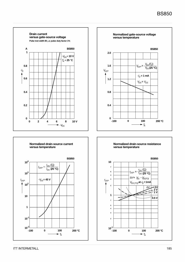
ITT INTERMETALL 185
BS850
Drain current versus gate-source voltage
A1
-ID
0.6
0.4
00
0.2
-VGS
10 V
Pulse test width 80 ms; pulse duty factor 1%
BS850
0.8
2 4 6 8
-V = 10 VDS
T = 25 °CA
Normalized drain-source current versus temperature
-100TA
200 °C
BS850104
103
102
10
1
10-2
0 100
IDSn
IDS (T )A
IDS (25 °C)
-V = 45 VDS
10-1
I =DSn
Normalized gate-source voltage versus temperature
VGS
-100TA
200 °C
BS8502.0
100
n
VGS (T )A
(25 °C)
-I = 1 mAD
1.6
1.2
0.8
0.4
00
V =GSn VGS
V = DS VGS
Normalized drain-source resistance versus temperature
10
1
-100TA
200 °C
BS850
10-1
0
rDSn
7
5
4
3
2
7
5
4
3
2
100
rDS (T )A
(25 °C)r =DSn rDS
∆V = V – V GS
GS (TO)V at -I = 1 mAD
> 3 V2 V1 V
0.5 V
∆V
GS(TO)
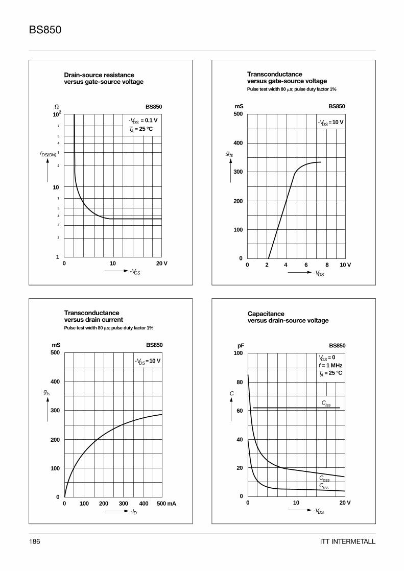
186 ITT INTERMETALL
BS850
Drain-source resistance versus gate-source voltage
V
rDS(ON)
1001
-VGS
20 V
BS850102
7
5
4
3
2
10
7
5
4
3
2
-V = 0.1 VDS
T = 25 °CA
Transconductance versus drain current
mS500
gfs
00
-ID
500 mA
Pulse test width 80 ms; pulse duty factor 1%
BS850
400
300
200
100
100 200 300 400
-V = 10 VDS
Transconductance versus gate-source voltage
mS500
gfs
00
-VGS
10 V
Pulse test width 80 ms; pulse duty factor 1%
BS850
400
300
200
100
2 4 6 8
-V = 10 VDS
Capacitance versus drain-source voltage
pF100
C
1000
-VDS
20 V
BS850
80
60
40
20
V = 0GSf = 1 MHzT = 25 °CA
Ciss
CossCrss

ITT INTERMETALL 187
BS850

188 ITT INTERMETALL
Darlington Transistors
ITT INTERMETALL 189
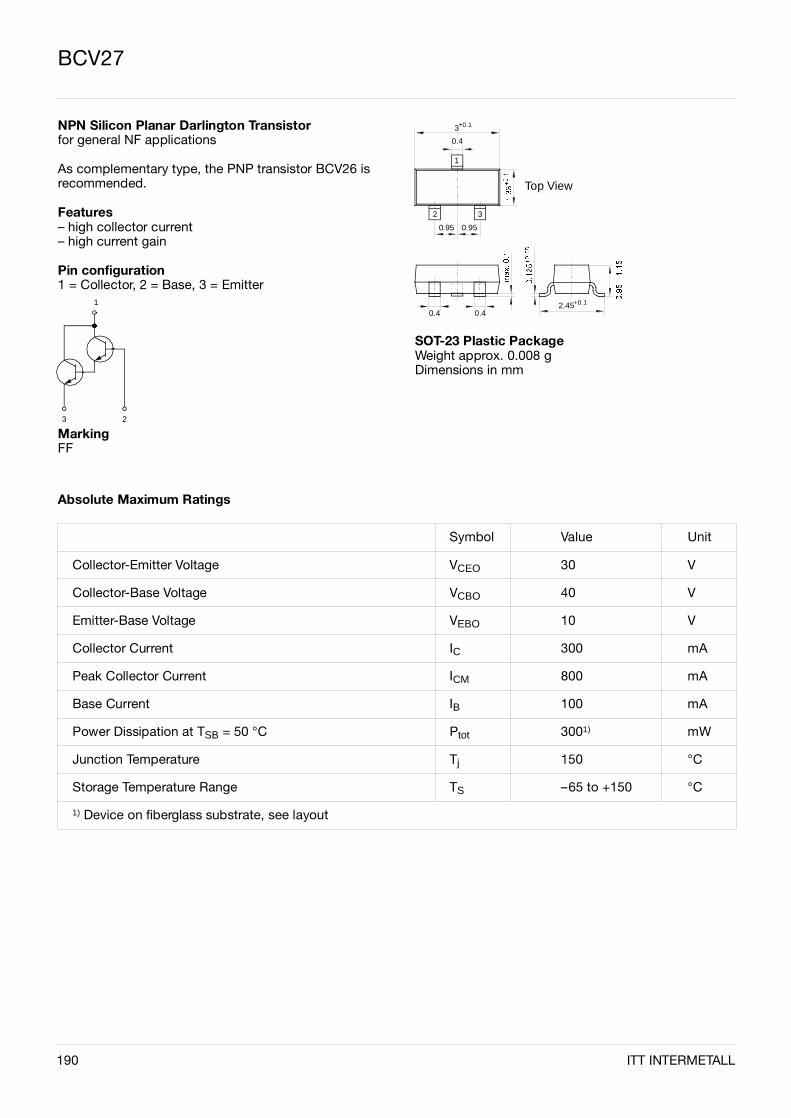
BCV27
Absolute Maximum Ratings
Symbol Value Unit
Collector-Emitter Voltage VCEO 30 V
Collector-Base Voltage VCBO 40 V
Emitter-Base Voltage VEBO 10 V
Collector Current IC 300 mA
Peak Collector Current ICM 800 mA
Base Current IB 100 mA
Power Dissipation at TSB = 50 °C Ptot 3001) mW
Junction Temperature Tj 150 °C
Storage Temperature Range TS –65 to +150 °C
1) Device on fiberglass substrate, see layout
NPN Silicon Planar Darlington Transistorfor general NF applications
As complementary type, the PNP transistor BCV26 isrecommended.
Features– high collector current– high current gain
Pin configuration1 = Collector, 2 = Base, 3 = Emitter
MarkingFF
3 2
1
190
0.4
0.95 0.95
3
0.4 0.4
+0.1
1
2 3
Top View
SOT-23 Plastic PackageWeight approx. 0.008 gDimensions in mm
2.45+0.1
ITT INTERMETALL
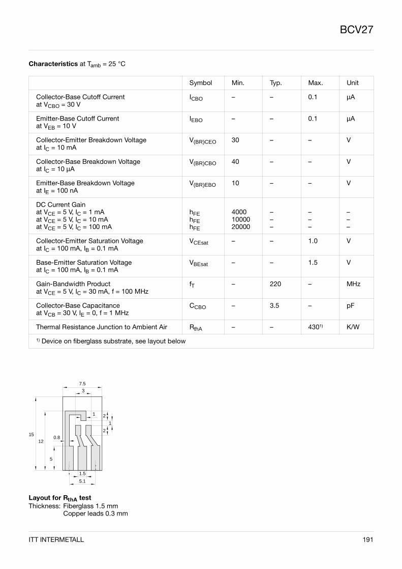
BCV27
Characteristics at Tamb = 25 °C
Symbol Min. Typ. Max. Unit
Collector-Base Cutoff Currentat VCBO = 30 V
ICBO – – 0.1 µA
Emitter-Base Cutoff Currentat VEB = 10 V
IEBO – – 0.1 µA
Collector-Emitter Breakdown Voltageat IC = 10 mA
V(BR)CEO 30 – – V
Collector-Base Breakdown Voltageat IC = 10 µA
V(BR)CBO 40 – – V
Emitter-Base Breakdown Voltageat IE = 100 nA
V(BR)EBO 10 – – V
DC Current Gainat VCE = 5 V, IC = 1 mAat VCE = 5 V, IC = 10 mAat VCE = 5 V, IC = 100 mA
hFEhFEhFE
40001000020000
–––
–––
–––
Collector-Emitter Saturation Voltageat IC = 100 mA, IB = 0.1 mA
VCEsat – – 1.0 V
Base-Emitter Saturation Voltageat IC = 100 mA, IB = 0.1 mA
VBEsat – – 1.5 V
Gain-Bandwidth Productat VCE = 5 V, IC = 30 mA, f = 100 MHz
fT – 220 – MHz
Collector-Base Capacitanceat VCB = 30 V, IE = 0, f = 1 MHz
CCBO – 3.5 – pF
Thermal Resistance Junction to Ambient Air RthA – – 4301) K/W
1) Device on fiberglass substrate, see layout below
Layout for RthA testThickness: Fiberglass 1.5 mm
Copper leads 0.3 mm
15 12
5
0.8
7.5
3
1
1.5
5.1
2
2
1
ITT INTERMETALL 191

BCV26
Absolute Maximum Ratings
Symbol Value Unit
Collector-Emitter Voltage –VCEO 30 V
Collector-Base Voltage –VCBO 40 V
Emitter-Base Voltage –VEBO 10 V
Collector Current –IC 300 mA
Peak Collector Current –ICM 800 mA
Base Current –IB 100 mA
Power Dissipation at TSB = 50 °C Ptot 3001) mW
Junction Temperature Tj 150 °C
Storage Temperature Range TS –65 to +150 °C
1) Device on fiberglass substrate, see layout
PNP Silicon Planar Darlington Transistorfor general NF applications
As complementary type, the NPN transistor BCV27 isrecommended.
Features– high collector current– high current gain
Pin configuration1 = Collector, 2 = Base, 3 = Emitter
MarkingFD
3 2
1
192
0.4
0.95 0.95
3
0.4 0.4
+0.1
1
2 3
Top View
SOT-23 Plastic PackageWeight approx. 0.008 gDimensions in mm
2.45+0.1
ITT INTERMETALL

BCV26
Characteristics at Tamb = 25 °C
Symbol Min. Typ. Max. Unit
Collector-Base Cutoff Currentat –VCBO = 30 V
–ICBO – – 0.1 µA
Emitter-Base Cutoff Currentat –VEB = 10 V
–IEBO – – 0.1 µA
Collector-Emitter Breakdown Voltageat –IC = 10 mA
–V(BR)CEO 30 – – V
Collector-Base Breakdown Voltageat IC = 10 µA
–V(BR)CBO 40 – – V
Emitter-Base Breakdown Voltageat –IE = 100 nA
–V(BR)EBO 10 – – V
DC Current Gainat –VCE = 5 V, –IC = 1 mAat –VCE = 5 V, –IC = 10 mAat –VCE = 5 V, –IC = 100 mA
hFEhFEhFE
40001000020000
–––
–––
–––
Collector-Emitter Saturation Voltageat –IC = 100 mA, –IB = 0.1 mA
–VCEsat – – 1.0 V
Base-Emitter Saturation Voltageat –IC = 100 mA, –IB = 0.1 mA
–VBEsat – – 1.5 V
Gain-Bandwidth Productat –VCE = 5 V, –IC = 30 mA, f = 100 MHz
fT – 220 – MHz
Collector-Base Capacitanceat –VCB = 30 V, IE = 0, f = 1 MHz
CCBO – 3.5 – pF
Thermal Resistance Junction to Ambient Air RthA – – 4301) K/W
1) Device on fiberglass substrate, see layout below
Layout for RthA testThickness: Fiberglass 1.5 mm
Copper leads 0.3 mm
15 12
5
0.8
7.5
3
1
1.5
5.1
2
2
1
ITT INTERMETALL 193

194 ITT INTERMETALL

ITT INTERMETALL 195
Bias Resistor Transistors

DTC114EK
Absolute Maximum Ratings
Symbol Value Unit
Supply Voltage VSUP 50 V
Input Voltage VI 40 V
–VI 10 V
Collector Current IC 50 mA
Peak Collector Current ICM 100 mA
Power Dissipation Ptot 3001) mW
Junction Temperature Tj 125 °C
Storage Temperature Range TS –65 to +125 °C
1) Device on fiberglass substrate, see layout
NPN Bias Resistor Transistor
The built-in bias resistor allows inverter circuit configu-ration without external resistors for input.
Pin configuration1 = Collector/OUT2 = Base/IN3 = Emitter/GND
MarkingEC4
Equivalent circuit
R1
R2
IN
IN
OUT R1 = 10 kΩ
GND R2 = 10 kΩ
OUT
GND
196
0.4
0.95 0.95
3
0.4 0.4
+0.1
1
2 3
Top View
SOT-23 Plastic PackageWeight approx. 0.008 gDimensions in mm
2.45+0.1
ITT INTERMETALL
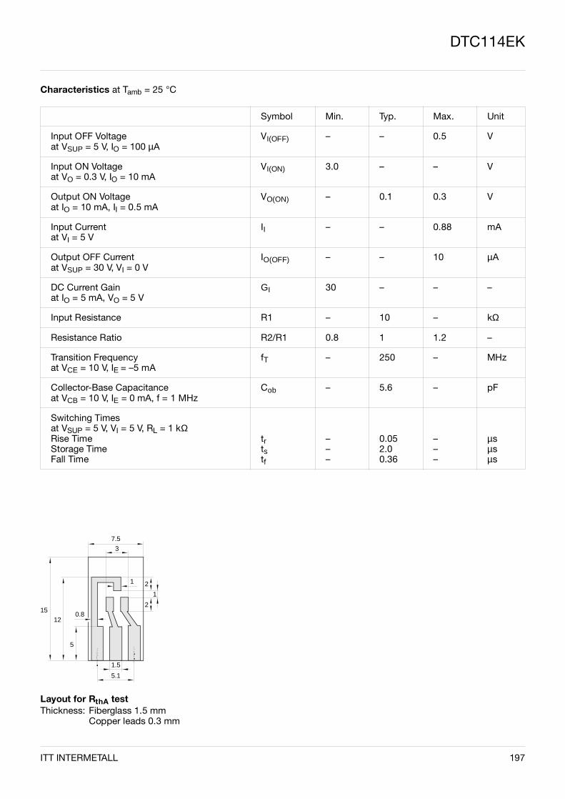
DTC114EK
Characteristics at Tamb = 25 °C
Symbol Min. Typ. Max. Unit
Input OFF Voltageat VSUP = 5 V, IO = 100 µA
VI(OFF) – – 0.5 V
Input ON Voltageat VO = 0.3 V, IO = 10 mA
VI(ON) 3.0 – – V
Output ON Voltageat IO = 10 mA, II = 0.5 mA
VO(ON) – 0.1 0.3 V
Input Currentat VI = 5 V
II – – 0.88 mA
Output OFF Currentat VSUP = 30 V, VI = 0 V
IO(OFF) – – 10 µA
DC Current Gainat IO = 5 mA, VO = 5 V
GI 30 – – –
Input Resistance R1 – 10 – kΩ
Resistance Ratio R2/R1 0.8 1 1.2 –
Transition Frequencyat VCE = 10 V, IE = –5 mA
fT – 250 – MHz
Collector-Base Capacitanceat VCB = 10 V, IE = 0 mA, f = 1 MHz
Cob – 5.6 – pF
Switching Timesat VSUP = 5 V, VI = 5 V, RL = 1 kΩRise TimeStorage TimeFall Time
trtstf
–––
0.052.00.36
–––
µsµsµs
Layout for RthA testThickness: Fiberglass 1.5 mm
Copper leads 0.3 mm
15 12
5
0.8
7.5
3
1
1.5
5.1
2
2
1
ITT INTERMETALL 197
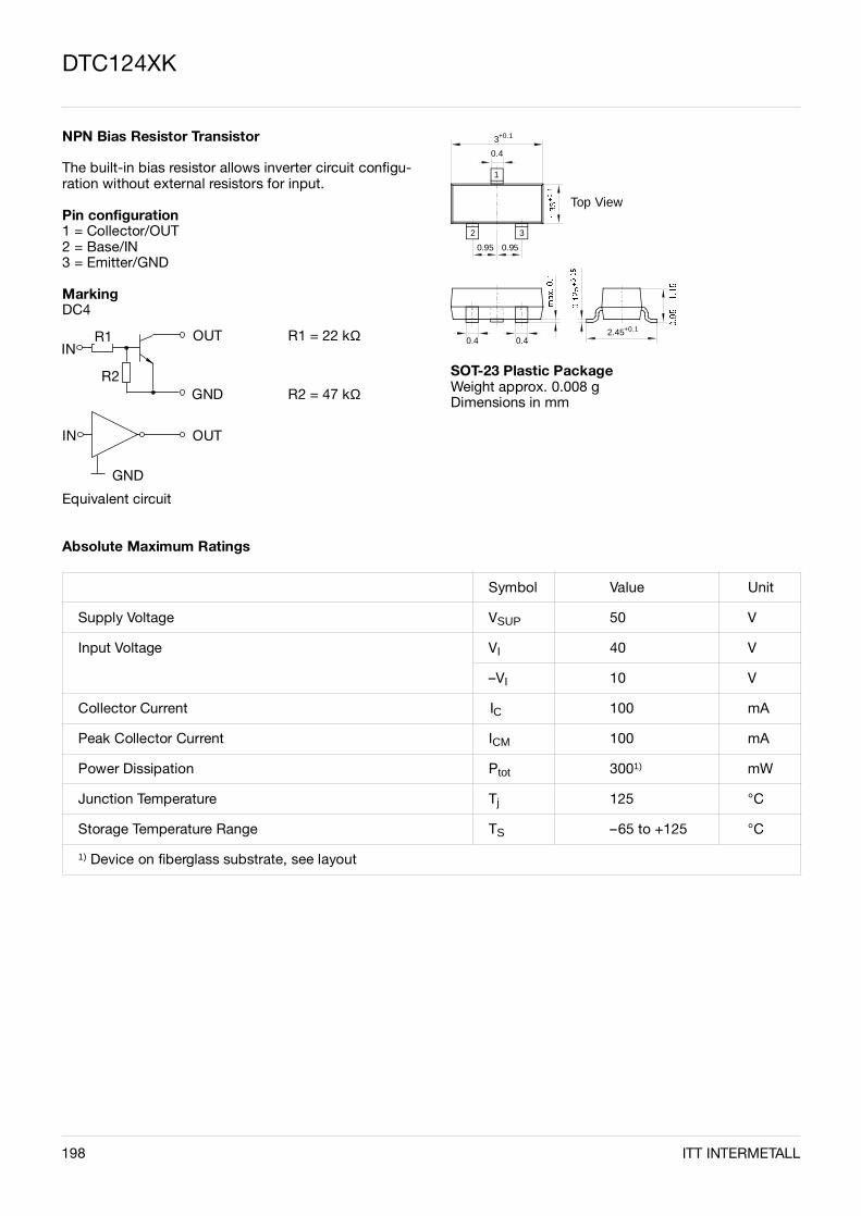
DTC124XK
Absolute Maximum Ratings
Symbol Value Unit
Supply Voltage VSUP 50 V
Input Voltage VI 40 V
–VI 10 V
Collector Current IC 100 mA
Peak Collector Current ICM 100 mA
Power Dissipation Ptot 3001) mW
Junction Temperature Tj 125 °C
Storage Temperature Range TS –65 to +125 °C
1) Device on fiberglass substrate, see layout
NPN Bias Resistor Transistor
The built-in bias resistor allows inverter circuit configu-ration without external resistors for input.
Pin configuration1 = Collector/OUT2 = Base/IN3 = Emitter/GND
MarkingDC4
Equivalent circuit
R1
R2
IN
IN
OUT R1 = 22 kΩ
GND R2 = 47 kΩ
OUT
GND
198
0.4
0.95 0.95
3
0.4 0.4
+0.1
1
2 3
Top View
SOT-23 Plastic PackageWeight approx. 0.008 gDimensions in mm
2.45+0.1
ITT INTERMETALL

DTC124XK
Characteristics at Tamb = 25 °C
Symbol Min. Typ. Max. Unit
Input OFF Voltageat VSUP = 5 V, IO = 100 µA
VI(OFF) – – 0.4 V
Input ON Voltageat VO = 0.3 V, IO = 2 mA
VI(ON) 2.5 – – V
Output ON Voltageat IO = 10 mA, II = 0.5 mA
VO(ON) – 0.1 0.3 V
Input Currentat VI = 0.5 V
II – – 0.36 mA
Output OFF Currentat VSUP = 30 V, VI = 0 V
IO(OFF) – – 10 µA
DC Current Gainat IO = 5 mA, VO = 5 V
GI 68 – – –
Input Resistance R1 – 22 – kΩ
Resistance Ratio R2/R1 1.7 2.1 2.6 –
Transition Frequencyat VCE = 10 V, IE = –5 mA
fT – 250 – MHz
Collector-Base Capacitanceat VCB = 10 V, IE = 0 mA, f = 1 MHz
Cob – 4.3 – pF
Switching Timesat VSUP = 5 V, VI = 5 V, RL = 1 kΩRise TimeStorage TimeFall Time
trtstf
–––
0.122.00.35
–––
µsµsµs
Layout for RthA testThickness: Fiberglass 1.5 mm
Copper leads 0.3 mm
15 12
5
0.8
7.5
3
1
1.5
5.1
2
2
1
ITT INTERMETALL 199

200 ITT INTERMETALL
ITT INTERMETALL 201
ITT INTERMETALL Sales Offices
GermanyITT INTERMETALLHans-Bunte-Strasse 19D-79108 FreiburgP.O. Box 840D-79008 FreiburgTel. ++49-761-517-0Fax ++49-761-517-2174
Hong KongITT Semiconductors (FE) Ltd.Room 5, 15th Floor, Block B,Veristrong Industrial CentreNo. 34-36, Au Pui Wan StreetFo Tan, ShatinNew TerritoriesHong KongTel. ++852-2688-0894Fax ++852-2687-4861
JapanITT Semiconductors (FE) Ltd.P.O. Box 4718th Floor, Sumitomo BuildingShinjuku-kuTokyo 163-02Tel. ++81-3-3347-8881Fax ++81-3-3347-8844
SingaporeITT Semiconductors (FE) Ltd.Representative Office150 Orchard Road # 07-13Orchard PlazaSingapore 0923Tel. ++65-732-65-66Fax ++65-737-73-92
United KingdomITT Semiconductors UK(for Discrete Semiconductors)Ms. Julie VollerJays CloseViables Industrial EstateBasingstokeHampshire RG22 4BWTel. ++44-1256-346-394Fax ++44-1256-346-395
ITT Semiconductors UK(for Integrated Circuits)Mr. John ThorogoodP.O. Box 1827GranboroughBucks. MK18 3ZTTel. ++44-1926-670-670Fax ++44-1926-670-676
ITT Semiconductors UK(for Integrated Circuits)Mr. Julian RichardsP.O. Box 81GuildfordSurrey GU2 6FYTel. ++44-1483-566-333Fax ++44-1483-566-332
USASales Headquarters:ITT Semiconductors2500 West Higgins RoadSuite 1015Hoffman Estates, IL 60195Tel. ++1-847-519-9610Fax ++1-847-519-9615
Central Area:ITT Semiconductors909 West Maumee StreetElmhurst BuildingAngola, IN 46703Tel. ++1-219-833-1960Fax ++1-219-665-2811
Western Area:ITT Semiconductors2635 North First StreetSuite 101San José, CA 95134Tel. ++1-408 526-2084Fax ++1-408 324-1379
202 ITT INTERMETALL
ITT INTERMETALL Distributors / Agents
AustraliaCRUSADER Electronic Components Pty. Ltd.P.O. Box 226Padstow NSW 2211Tel. (02) 792 3922Fax (02) 792 1446
AustriaTRANSOHMVertriebsgesellschaft m.b.H.Kolbegasse 68A-1232 WienTel. (0431) 6 10 66-0Fax (0431) 6 10 66-10
SPOERLE ELECTRONICDistribution International GmbHHeiligenstädter Strasse 52A-1190 WienTel. (02 22) 36 36 50-0Fax (02 22) 3 69 22 73
BelgiumSPOERLE ELECTRONICDistribution International GmbHKeiberg IIMinervastraat, 14/B2B-1930 ZaventemTel. (02) 725 46 60Fax (02) 725 45 11
CanadaFarnell Electronic Services300 North Rivermede RoadConcord, Ontario L4K 2Z4Tel. (416) 798-4884Fax (416) 798-4889
ChinaWalasey Ltd.Shanghai Liaison OfficeRoom 1708, Block 1Hu Ban Building1250, Zhong Shan Rd., North, #1ShanghaiP.R.C.Tel. (21) 516-1882 or (21) 542-4152Fax (21) 542-4152
Czech RepublicSPOERLE ELECTRONIC spol. s.r.o.Charkovska 24101 00 PrahaTel. (2) 73 13 55 Fax (2) 73 13 54
DenmarkFarnell Electronic ServicesNaverland 29DK-2600 GlostrupTel. (42) 45 66 45Fax (42) 45 07 86
FinlandFarnell Electronic ServicesTyöpajakatu 5SF-00580 HelsinkiTel. (0) 4766-0Fax (0) 4766-6318
FranceARROW ELECTRONIQUE78-79, rue des SoletsSilic 585F-94663 Rungis CEDEXTel. (1) 49 78 49 78Fax (1) 49 78 05 96
Farnell Electronic ServicesP.O. Box 69 - St. AubinF-91192 Gif s/Yvette CEDEX Tel. (1) 6 98 58-383Fax (1) 6 98 58-399
Dimacel Composants63, rue Jean JauresP.O. Box 116F-95874 Bezons CEDEXTel. (1) 34 23 70 00Fax (1) 30 76 31 97
ITT INTERMETALLMr. Francois BoubetAgent Technico-Commercial11, rue de RimoronF-91650 Breux-JouyTel. (1) 64 58 60 60Fax (1) 64 58 60 60
RutronikComposants ElectroniquesLe SaillantF-19130 VoutezacTel. (55) 84 74 83Fax (55) 84 79 00
GermanyBeck GmbH & Co. Eltersdorfer Strasse 7D-90425 Nürnberg Tel. (0911) 9 34 08-0Fax (0911) 9 34 08-28
Farnell Electronic ServicesBahnhofstrasse 44D-71696 MöglingenTel. (07141) 487-0Fax (07141) 487-210
Future Electronics Deutschland GmbHMünchner Str. 18D-85774 UnterföhringTel. (089) 957 27-0Fax (089) 957 27-173
RUTRONIKElektronische BauelementeGmbHRSC-Halbleiter GmbHIndustriestrasse 2D-75228 IspringenTel. (07231) 801-0Fax (07231) 822 82
SPOERLE ELECTRONICMax-Planck-Strasse 1-3D-63303 Dreieich Tel. (06103) 304-8Fax (06103) 304-455
Hong KongWalasey Ltd. Room 1010, 10th FloorAPEC PlazaNo. 49, Hoi Yuen RoadKwun TongKowloon Hong KongTel. 2357-1676Fax 2357-1189
ARRAY Electronics Ltd.24th Floor, Wyler Centre, Phase 2No. 200, Tai Lin Pai RoadKwai ChungNew TerritoriesHong KongTel. 2418-3700 or 2418-3800Fax 2418-6992 or 2418-6993
ItalyTARA S.R.L.Viale Milanofiori, E5I-20090 Assago (Milano)Tel. (02) 82 470 232Fax (02) 82 426 31
Silverstar Ltd. S.P.A.Viale Fulvio Testi, 28020126 Milano, MITel. (02) 66 12 51Fax (02) 66 10 13 59
Rebosio Componenti S.P.A.Viale G. Prati, 320051 Limbiate (Milano)Tel. (02) 99 65 767Fax (02) 99 62 968
Farnell S.P.A.Viale Milanofiori E/520094 Assago (Milano)Tel. (02) 82 470Fax (02) 82 42 631
Eurodis Fanton S.R.L.Via Olindo Simoni, 840011 Anzola d’Emilia, BOTel. (05) 17 35 015Fax (05) 17 35 013
JapanUNI Electronics Inc. P.O. Box 68Sumitomo BuildingShinjuku-kuTokyo 163Tel. (03) 33 47-8878Fax (03) 33 47-8808
KoreaSOEI KOREA Inc.WooNam Building, 4th Floor824-22, Yeoksam-dongKangnam-kuSeoul 135-080Tel. (02) 508 3221Fax (02) 508 3229
NetherlandsSPOERLE ELECTRONICDistribution International GmbHColtbaan 17NL-3439 NG NieuwegeinTel. (03402) 912 34Fax (03402) 467 64/359 24
Farnell Electronic ServicesChroomstraat 28NL-2718 RR ZoetermeerTel. (079) 613-161Fax (079) 613-169
ITT INTERMETALL 203
ITT INTERMETALL Distributors / Agents
NorwayFarnell Electronic ServicesKarihaugun 89N-1001 Oslo Tel. (47) 2232-1270Fax (47) 2232-5120
PolandSPOERLE ELECTRONICPolska Sp. z.o.o. ul. Domaniewska 4102-672 WarschauTel. (22) 640 03 49or (22) 640 04 47/48/49Fax (22) 640 03 48
SingaporeUNI Electronics PTE. Ltd.1 Tanglin Road #03-260Orchard Parade Hotel(Podium Block)Singapore 1024Tel. (+65) 235 77 40or (+65) 235 82 57 Fax (+65) 235 52 98
South AfricaElectronic Building Elements (Pty) Ltd.P.O. Box 912-1222Silverton, 0127Tel. (012) 803-7680Fax (012) 803-8294
SpainAKTA SPAIN S.A.Roger de Llúria, 155ENTLO 2.a
E-08037 BarcelonaTel. (3) 218 49 49 - 415 22 66Fax (3) 237 07 80
AMITRON-ARROW S.A.Albasanz, 75E-28037 MadridTel. (1) 304 30 40Fax (1) 327 24 72
SwedenFarnell Electronic ServicesAnkdammsgatan 32P.O. Box 1330S-17126 SolnaTel. (08) 83 00 20Fax (08) 27 13 03
Ericsson ProcompIsafjordsgatan 16S-16481 Kista-StockholmTel. (08) 757 40 40Fax (08) 757 41 10
SwitzerlandFarnell Electronic ServicesBrandschenkestrasse 178CH-8027 ZürichTel. (01) 2 04 61 11Fax (01) 2 04 64 54
AKTA Multikomponent AGAlte Steinhauserstr. 3Postfach 5039CH-6330 ChamTel. (041) 740 14 42Fax (041) 740 13 23
SPOERLE ELECTRONICDistribution International GmbHCherstr. 4PostfachCH-8152 Opfikon-GlattbruggTel. (01) 1 874 6262Fax (01) 1 874 6200
SPOERLE ELECTRONICDistribution International GmbHEn ChamardCH-1442 Montagny s/YverdonTel. (024) 27 01 00Fax (024) 24 52 45
TaiwanWesTech Electronics, Inc.P.O. Box 55-04665F, No. 197Ho Ping E. Road, Sec. 1Taipei, Taiwan 106, R.O.C.Tel. (02) 356-0620Fax (02) 394-2047
TurkeyBIGSTARElektronik Sanayi ve Ticaret A.S.Okcu Musa Cad. 69/2TR-80020 Karaköy-IstanbulTel. (0) 212 252 59 15 (3 lines)Fax (0) 212 252 54 38
INTER A.S.Kadiköy HasircibasiCaddesi No. 55TR-81310 IstanbulTel. (0) 216 349 94 00 (30 lines)Fax (0) 216 349 94 30
United KingdomARROW Electronics (UK) Ltd.St. Martins Business CentreCambridge RoadBedford MK42 0LFTel. (01234) 34 72 11Fax (01234) 21 46 74
Farnell Electronic ServicesEdinburgh WayHarlow, EssexCM20 2DFTel. (01279) 44 11 44Fax (01279) 44 16 87
First Principals Ltd.2 Walker RoadBardon HillCoalvilleLeicestershire LE67 1TUTel. (01530) 51 12 95Fax (01530) 51 12 96
Flint Distribution Ltd.Enterprise HouseAshby RoadCoalvilleLeicestershire LE67 3LATel. (01530) 51 03 35Fax (01530) 51 02 75
Future Electronics Ltd. Future HousePoyle RoadColnbrook Slough, Berks.SL3 0EZTel. (01075) 368 70 00Fax (01075) 368 91 00
HB Electronics Ltd.Lever StreetBolton, Lancs.B13 6BJTel. (01204) 38 63 61Fax (01204) 38 49 11
Farnell Electronic Services346 Edinburgh AvenueSloughSL1 4TUTel. (01753) 82 42 12Fax (01753) 82 41 60
USADiodes Incorporated3050 East Hillcrest DriveWestlake Village, CA 91362Tel. (805) 446-4800Fax (805) 446-4850
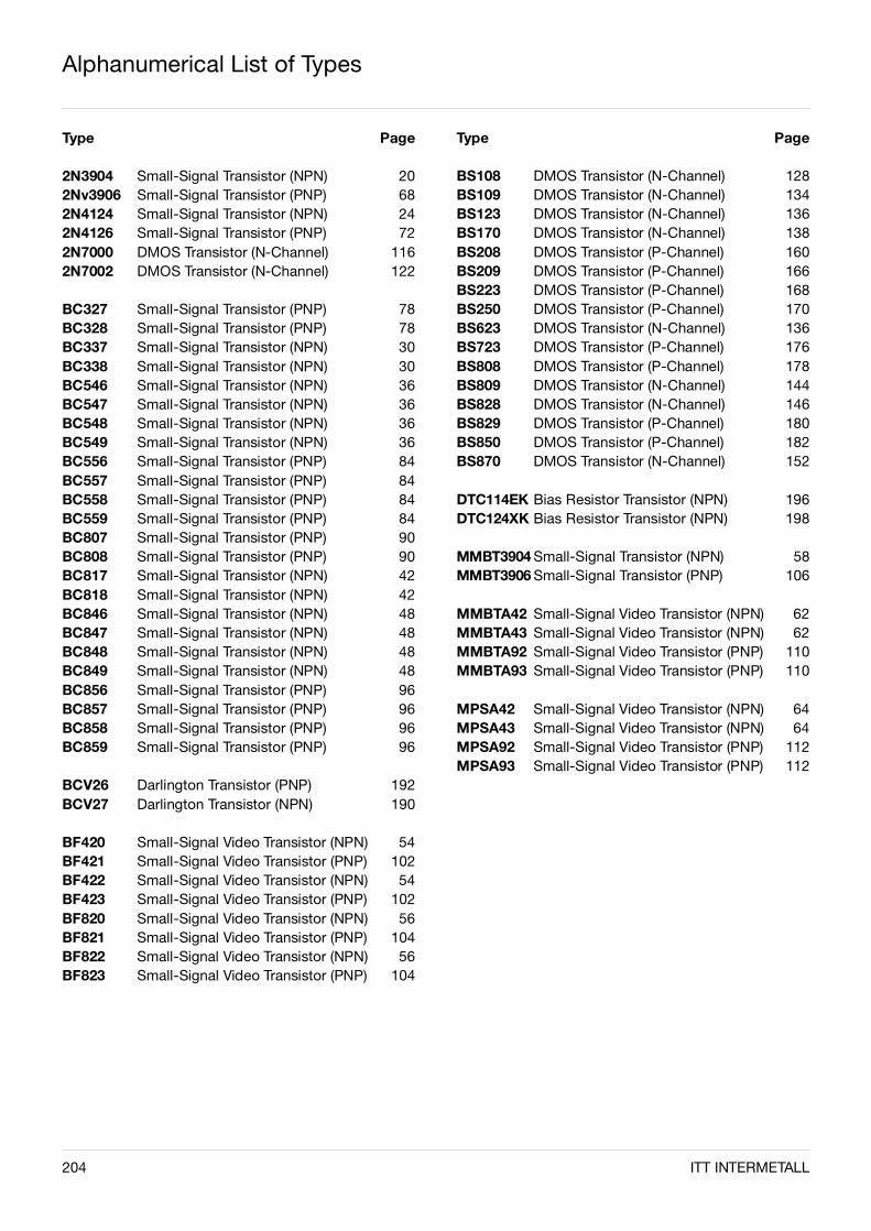
204 ITT INTERMETALL
Type Page
2N3904 Small-Signal Transistor (NPN) 202Nv3906 Small-Signal Transistor (PNP) 682N4124 Small-Signal Transistor (NPN) 242N4126 Small-Signal Transistor (PNP) 722N7000 DMOS Transistor (N-Channel) 1162N7002 DMOS Transistor (N-Channel) 122
BC327 Small-Signal Transistor (PNP) 78BC328 Small-Signal Transistor (PNP) 78BC337 Small-Signal Transistor (NPN) 30BC338 Small-Signal Transistor (NPN) 30BC546 Small-Signal Transistor (NPN) 36BC547 Small-Signal Transistor (NPN) 36BC548 Small-Signal Transistor (NPN) 36BC549 Small-Signal Transistor (NPN) 36BC556 Small-Signal Transistor (PNP) 84BC557 Small-Signal Transistor (PNP) 84BC558 Small-Signal Transistor (PNP) 84BC559 Small-Signal Transistor (PNP) 84BC807 Small-Signal Transistor (PNP) 90BC808 Small-Signal Transistor (PNP) 90BC817 Small-Signal Transistor (NPN) 42BC818 Small-Signal Transistor (NPN) 42BC846 Small-Signal Transistor (NPN) 48BC847 Small-Signal Transistor (NPN) 48BC848 Small-Signal Transistor (NPN) 48BC849 Small-Signal Transistor (NPN) 48BC856 Small-Signal Transistor (PNP) 96BC857 Small-Signal Transistor (PNP) 96BC858 Small-Signal Transistor (PNP) 96BC859 Small-Signal Transistor (PNP) 96
BCV26 Darlington Transistor (PNP) 192BCV27 Darlington Transistor (NPN) 190
BF420 Small-Signal Video Transistor (NPN) 54BF421 Small-Signal Video Transistor (PNP) 102BF422 Small-Signal Video Transistor (NPN) 54BF423 Small-Signal Video Transistor (PNP) 102BF820 Small-Signal Video Transistor (NPN) 56BF821 Small-Signal Video Transistor (PNP) 104BF822 Small-Signal Video Transistor (NPN) 56BF823 Small-Signal Video Transistor (PNP) 104
Type Page
BS108 DMOS Transistor (N-Channel) 128BS109 DMOS Transistor (N-Channel) 134BS123 DMOS Transistor (N-Channel) 136BS170 DMOS Transistor (N-Channel) 138BS208 DMOS Transistor (P-Channel) 160BS209 DMOS Transistor (P-Channel) 166BS223 DMOS Transistor (P-Channel) 168BS250 DMOS Transistor (P-Channel) 170BS623 DMOS Transistor (N-Channel) 136BS723 DMOS Transistor (P-Channel) 176BS808 DMOS Transistor (P-Channel) 178BS809 DMOS Transistor (N-Channel) 144BS828 DMOS Transistor (N-Channel) 146BS829 DMOS Transistor (P-Channel) 180BS850 DMOS Transistor (P-Channel) 182BS870 DMOS Transistor (N-Channel) 152
DTC114EK Bias Resistor Transistor (NPN) 196DTC124XK Bias Resistor Transistor (NPN) 198
MMBT3904 Small-Signal Transistor (NPN) 58MMBT3906 Small-Signal Transistor (PNP) 106
MMBTA42 Small-Signal Video Transistor (NPN) 62MMBTA43 Small-Signal Video Transistor (NPN) 62MMBTA92 Small-Signal Video Transistor (PNP) 110MMBTA93 Small-Signal Video Transistor (PNP) 110
MPSA42 Small-Signal Video Transistor (NPN) 64MPSA43 Small-Signal Video Transistor (NPN) 64MPSA92 Small-Signal Video Transistor (PNP) 112MPSA93 Small-Signal Video Transistor (PNP) 112
Alphanumerical List of Types
INTERMETALL semiconductors
ITT INTERMETALL Printed in GermanyHans-Bunte-Strasse 19 Edition 1996D-79108 Freiburg (Germany) Order No. 6240-15-1EP.O. Box 840D-79008 Freiburg (Germany)Tel. +49-7 61-5 17-0Fax +49-7 61-5 17-21 74E-mail: [email protected]: http://www.itt-sc.de


