FUJITSU SEMICONDUCTOR DATA SHEET Copyright 2016 FUJITSU SEMICONDUCTOR LIMITED 2016.10 Memory FRAM 64 K (8 K × 8) Bit I 2 C MB85RC64TA ■ DESCRIPTION The MB85RC64TA is an FRAM (Ferroelectric Random Access Memory) chip in a configuration of 8,192 words × 8 bits, using the ferroelectric process and silicon gate CMOS process technologies for forming the nonvolatile memory cells. Unlike SRAM, the MB85RC64TA is able to retain data without using a data backup battery. The read/write endurance of the nonvolatile memory cells used for the MB85RC64TA has improved to be at least 10 13 cycles, significantly outperforming Flash memory and E 2 PROM in the number. The MB85RC64TA does not need a polling sequence after writing to the memory such as the case of Flash memory or E 2 PROM. ■ FEATURES • Bit configuration : 8,192 words × 8 bits • Two-wire serial interface : Fully controllable by two ports: serial clock (SCL) and serial data (SDA). • Operating frequency : 3.4 MHz (Max @HIGH SPEED MODE) 1 MHz (Max @FAST MODE PLUS) • Read/write endurance : 10 13 times / byte • Data retention : 10 years ( + 85 °C), 95 years ( + 55 °C), over 200 years ( + 35 °C) • Operating power supply voltage : 1.8 V to 3.6 V • Low power consumption : Operating power supply current 170 μA (Typ @3.4 MHz) Standby current 8 μA (Typ) Sleep current 4 μA (Typ) • Operation ambient temperature range : − 40 °C to + 85 °C • Package : 8-pin plastic SOP (FPT-8P-M09) 8-pin plastic SON (LCC-8P-M04) RoHS compliant DS501-00044-2v0-E
Transcript
FUJITSU SEMICONDUCTORDATA SHEET DS501-00044-2v0-E
Memory FRAM
64 K (8 K × 8) Bit I2C
MB85RC64TA
■ DESCRIPTIONThe MB85RC64TA is an FRAM (Ferroelectric Random Access Memory) chip in a configuration of 8,192 words × 8 bits, using the ferroelectric process and silicon gate CMOS process technologies for forming thenonvolatile memory cells.
Unlike SRAM, the MB85RC64TA is able to retain data without using a data backup battery.
The read/write endurance of the nonvolatile memory cells used for the MB85RC64TA has improved to beat least 1013 cycles, significantly outperforming Flash memory and E2PROM in the number.
The MB85RC64TA does not need a polling sequence after writing to the memory such as the case of Flashmemory or E2PROM.
■ FEATURES• Bit configuration : 8,192 words × 8 bits• Two-wire serial interface : Fully controllable by two ports: serial clock (SCL) and serial data (SDA).• Operating frequency : 3.4 MHz (Max @HIGH SPEED MODE)
1 MHz (Max @FAST MODE PLUS)• Read/write endurance : 1013 times / byte• Data retention : 10 years ( + 85 °C), 95 years ( + 55 °C), over 200 years ( + 35 °C)• Operating power supply voltage : 1.8 V to 3.6 V• Low power consumption : Operating power supply current 170 μA (Typ @3.4 MHz)
Standby current 8 μA (Typ)Sleep current 4 μA (Typ)
• Operation ambient temperature range : − 40 °C to + 85 °C• Package : 8-pin plastic SOP (FPT-8P-M09)
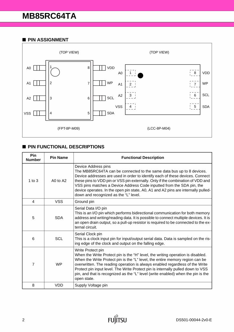
Device Address pinsThe MB85RC64TA can be connected to the same data bus up to 8 devices. Device addresses are used in order to identify each of these devices. Connect these pins to VDD pin or VSS pin externally. Only if the combination of VDD and VSS pins matches a Device Address Code inputted from the SDA pin, the device operates. In the open pin state, A0, A1 and A2 pins are internally pulled-down and recognized as the “L” level.
4 VSS Ground pin
5 SDA
Serial Data I/O pinThis is an I/O pin which performs bidirectional communication for both memory address and writing/reading data. It is possible to connect multiple devices. It is an open drain output, so a pull-up resistor is required to be connected to the ex-ternal circuit.
6 SCLSerial Clock pinThis is a clock input pin for input/output serial data. Data is sampled on the ris-ing edge of the clock and output on the falling edge.
7 WP
Write Protect pinWhen the Write Protect pin is the “H” level, the writing operation is disabled. When the Write Protect pin is the “L” level, the entire memory region can be overwritten. The reading operation is always enabled regardless of the Write Protect pin input level. The Write Protect pin is internally pulled down to VSS pin, and that is recognized as the “L” level (write enabled) when the pin is the open state.
8 VDD Supply Voltage pin
VSS SDA
A1
VDD
SCLA2
A0
WP
8
7
6
54
3
2
1
(TOP VIEW)
(FPT-8P-M09)
(TOP VIEW)
(LCC-8P-M04)
2
3
4
1
7
6
5
8
VSS SDA
A1
VDD
SCLA2
A0
WP
2 DS501-00044-2v0-E
MB85RC64TA
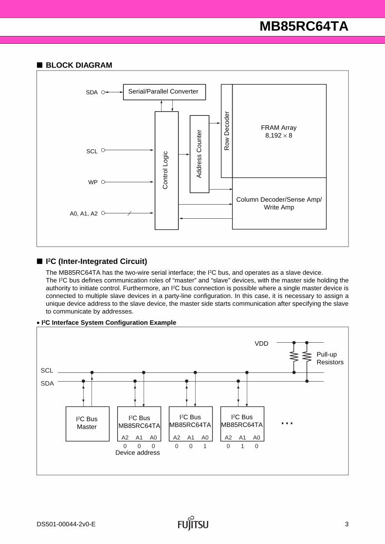
■ BLOCK DIAGRAM
■ I2C (Inter-Integrated Circuit)The MB85RC64TA has the two-wire serial interface; the I2C bus, and operates as a slave device. The I2C bus defines communication roles of “master” and “slave” devices, with the master side holding theauthority to initiate control. Furthermore, an I2C bus connection is possible where a single master device isconnected to multiple slave devices in a party-line configuration. In this case, it is necessary to assign aunique device address to the slave device, the master side starts communication after specifying the slaveto communicate by addresses.
• I2C Interface System Configuration Example
WP
A0, A1, A2
SDA
SCL Row
Dec
oder
Add
ress
Cou
nter
FRAM Array8,192 × 8
Serial/Parallel Converter
Column Decoder/Sense Amp/Write Amp
Con
trol
Log
ic
SCL
SDA
A2 A1 A0
0 0 0
A2 A1 A0
0 0 1
A2 A1 A0
0 1 0
...I2C Bus Master
I2C BusMB85RC64TA
I2C BusMB85RC64TA
I2C BusMB85RC64TA
Pull-up Resistors
Device address
VDD
DS501-00044-2v0-E 3
MB85RC64TA
■ I2C COMMUNICATION PROTOCOL The I2C bus is a two wire serial interface that uses a bidirectional data bus (SDA) and serial clock (SCL). Adata transfer can only be initiated by the master, which will also provide the serial clock for synchronization.The SDA signal should change while the SCL is the “L” level. However, as an exception, when starting andstopping communication sequence, the SDA is allowed to change while the SCL is the “H” level.
• Start Condition
To start read or write operations by the I2C bus, change the SDA input from the “H” level to the “L” level whilethe SCL input is in the “H” level.
• Stop Condition
To stop the I2C bus communication, change the SDA input from the “L” level to the “H” level while the SCLinput is in the “H” level. In the reading operation, inputting the stop condition finishes reading and enters thestandby state. In the writing operation, inputting the stop condition finishes inputting the rewrite data andenters the standby state.
• Start Condition, Stop Condition
Note : At the write operation, the FRAM device does not need the programming wait time (tWC) after issuing the Stop Condition.
SCL
SDA
Start Stop
“H” or “L”
4 DS501-00044-2v0-E
MB85RC64TA
■ ACKNOWLEDGE (ACK)In the I2C bus, serial data including address or memory information is sent in units of 8 bits. The acknowledgesignal indicates that every 8 bits of the data is successfully sent and received. The receiver side usuallyoutputs the “L” level every time on the 9th SCL clock after each 8 bits are successfully transmitted andreceived. On the transmitter side, the bus is temporarily released to Hi-Z every time on this 9th clock to allowthe acknowledge signal to be received and checked. During this Hi-Z-released period, the receiver side pullsthe SDA line down to indicate the “L” level that the previous 8 bits communication is successfully received.
In case the slave side receives Stop condition before sending or receiving the ACK “L” level, the slave sidestops the operation and enters to the standby state. On the other hand, the slave side releases the bus stateafter sending or receiving the NACK “H” level. The master side generates Stop condition or Start conditionin this released bus state.
• Acknowledge timing overview diagram
SCL 1 2 3 8 9
SDA
Start
ACK
The transmitter side should always release SDA on the 9th bit. At this time, the receiver side outputs a pull-down if the previous 8 bits data are received correctly (ACK re-sponse).
DS501-00044-2v0-E 5
MB85RC64TA
■ DEVICE ADDRESS WORD (Slave address) Following the start condition, the master sends the 8 bits device address word to start I2C communication.The device address word (8 bits) consists of a device Type code (4 bits), device address code (3 bits), anda read/write code (1 bit).
• Device Type Code (4 bits)
The upper 4 bits of the device address word are a device type code that identifies the device type, and arefixed at “1010” for the MB85RC64TA.
• Device Address Code (3 bits)
Following the device type code, the 3 bits of the device address code are input in order of A2, A1 and A0.The device address code identifies one device from up to eight devices connected to the bus. Each MB85RC64TA is given a unique 3 bits code on the device address pin (external hardware pin A2, A1and A0). The slave only responds if the received device address code is equal to this unique 3 bits code.
• Read/Write Code (1 bit)
The 8th bit of the device address word is the R/W (read/write) code. When the R/W code is “0”, a writeoperation is enabled, and the R/W code is “1”, a read operation is enabled for the MB85RC64TA.
It turns to a stand-by state if the device code is not “1010” or device address code does not equal to pinsA2, A1 and A0.
• Device Address Word
. .
. .
Start
ACK (SDA is the "L" level)
1 2 3 4 5 6 7 8 9 1 2
SCL
SDA ACK
Start Condition
Device Code Device Address Code Read/Write Code
A
S
S 1 0 1 0 A2 A1 A0 R/W A
Access from master
Access from slave
6 DS501-00044-2v0-E
MB85RC64TA
■ DATA STRUCTUREIn the I2C bus, the acknowledge “L” level is output on the 9th bit by a slave, after the 8 bits of the deviceaddress word following the start condition are input by a master. After confirming the acknowledge responseby the master, the master outputs 8 bits × 2 memory address to the slave. When the each memory addressinput ends, the slave again outputs the acknowledge “L” level. After this operation, the I/O data follows inunits of 8 bits, with the acknowledge “L” level output after every 8 bits.
It is determined by the R/W code whether the data line is driven by the master or the slave. However, theclock line shall be driven by the master. For a write operation, the slave will accept 8 bits from the master,then send an acknowledge. If the master detects the acknowledge, the master will transfer the next 8 bits.For a read operation, the slave will place 8 bits on the data line, then wait for an acknowledge from the master.
■ FRAM ACKNOWLEDGE -- POLLING NOT REQUIREDThe MB85RC64TA performs write operations at the same speed as read operations, so any waiting time foran ACK polling* does not occur. The write cycle takes no additional time.
*: In E2PROM, the Acknowledge Polling is performed as a progress check whether rewriting is executed or not.It is normal to judge by the 9th bit of Acknowledge whether rewriting is performed or not after inputting the start condition and then the device address word (8 bits) during rewriting.
■ WRITE PROTECT (WP) The entire memory array can be write protected using the Write Protect pin. When the Write Protect pin isset to the “H” level, the entire memory array will be write protected. When the Write Protect pin is the “L”level, entire memory array will be rewritten. Reading is allowed regardless of the WP pin's “H” level or “L” level.
Note : The Write Protect pin is pulled down internally to VSS pin, therefore if the Write Protect pin is open, the pin status is detected as the “L” level (write enabled).
DS501-00044-2v0-E 7
MB85RC64TA
■ COMMAND• Byte Write
If the device address word (R/W “0” input) is sent following the start condition, the slave responds with anACK. After this ACK, write addresses and data are sent in the same way, and the write ends by generatinga stop condition at the end.
Note : In the MB85RC64TA, input “000” as the upper 3 bits of the MSB.
• Page Write
If additional 8 bits are continuously sent after the same command (except stop condition) as Byte Write, apage write is performed. The memory address rolls over to first memory address (0000H) at the end of theaddress. Therefore, if more than 8 Kbytes are sent, the data is overwritten in order starting from the start ofthe memory address that was written first. Because FRAM performs the high-speed write operations, thedata will be written to FRAM right after the ACK response finished.
Note : It is not necessary to take a period for internal write operation cycles from the buffer to the memory after the stop condition is generated.
LSB
Start Condition
Stop Condition
ACK (SDA is the "L" level)A
S
P
MSB
0 0 0 X X X X X X X X X X X X X
S A2 A1 A0 A A A A PAddress
High 8bitsAddressLow 8bits
Write Data 8bits01 0 1 0
Access from master
Access from slave
Start Condition
Stop Condition
ACK (SDA is the "L" level)A
S
P
S A2 A1 A0 A A A A A PAddress
High 8bitsAddressLow 8bits
Write Data 8bits
Write Data ...01 0 1 0
Access from master
Access from slave
8 DS501-00044-2v0-E
MB85RC64TA
• Current Address Read
When the previous write or read operation finishes successfully up to the stop condition and assumes thelast accessed address is “n”, then the address at “n+1” is read by sending the following command unlessturning the power off. If the memory address is last address, the address counter will roll over to 0000H. Thecurrent address in memory address buffer is undefined immediately after the power is turned on.
• Random Read
The one byte of data from the memory address saved in the memory address buffer can be read outsynchronously to SCL by specifying the address in the same way as for a write, and then issuing anotherstart condition and sending the Device Address Word (R/W “1” input).
The final NACK is issued by the receiver that receives the data. In this case, this bit is issued by the masterside.
Start Condition
Stop Condition
ACK(SDA is the "L" level)A
S
P
NACK (SDA is the "H" level)N
S A2 A1 A0 A N PRead
Data 8bits
(n+1) address
11 0 1 0
Access from master
Access from slave
Start Condition
Stop Condition
ACK (SDA is the "L" level)A
S
P
NACK (SDA is the "H" level)N
S A2 A1 A0 A A A PAddress
High 8bitsAddressLow 8bits01 0 1 0 S A2 A1 A0 A11 0 1 0
Read Data 8bits N
Access from master
Access from slave
DS501-00044-2v0-E 9
MB85RC64TA
• Sequential Read
Data can be received continuously following the Device address word (R/W “1” input) after specifying theaddress in the same way as for Random Read. If the read reaches the end of address, the internal readaddress automatically rolls over to first memory address 0000H and keeps reading.
Stop Condition
ACK (SDA is the "L" level)A
P
NACK (SDA is the "H" level)N
A A A N PRead Data 8bits
Read Data 8bits
ReadData
......
Access from master
Access from slave
10 DS501-00044-2v0-E
MB85RC64TA
• High Speed Mode
MB85RC64TA supports High Speed mode up to 3.4 MHz. By sending an entry command (0000 1XXX) afterstart condition from the master side, it informs to the slave that the data transmission with High Speed modewill start.
Since there is no slave side which is allowed to respond to this entry command, NACK response continuesfrom the slave side. After the master side recognizes this NACK response, the master side changes its stateto High Speed mode and enables the bidirectional communication up to 3.4 MHz.
By sending Stop condition, it exits out of the state in High Speed communication.
A
S
P
N
S A2 A1 A N PRead
Data 8bits11 0 1 0 A0S 1 X NX0 0 0 0 X
A A A N PRead Data 8bits
Read Data 8bits
ReadData
......
S A2 A1 A A A A PAddress
High 8bitsAddress
Low 8bitsWrite
Data 8bits01 0 1 0 A0S 1 X NX0 0 0 0 X
S A2 A1 A A A A A PAddress
High 8bitsAddress
Low 8bitsWrite
Data 8bitsWrite Data0 ...1 0 1 0 A0S 1 X NX0 0 0 0 X
S A2 A1 A A A PAddress
High 8bitsAddressLow 8bits01 0 1 0 S A2 A1 A11 0 1 0
Read Data 8bits NA0 A0S 1 X NX0 0 0 0 X
S A2 A1 A A AAddress
High 8bitsAddressLow 8bits01 0 1 0 S A2 A1 A11 0 1 0
Read Data 8bits AA0 A0S 1 X NX0 0 0 0 X ...
A
N
Access from master
Access from slave
Start Condition
Stop ConditionACK(SDA is the “L” level)NACK(SDA is the “H” level)
Byte Write @High Speed Mode
Page Write @High Speed Mode
Current Address Read @High Speed Mode
Random Address Read @High Speed Mode
Sequential Read @High Speed Mode
High Speed ModeStandard ModeFast ModeFast Mode Plus
DS501-00044-2v0-E 11
MB85RC64TA
• Sleep Mode
MB85RC64TA provides Sleep mode which reduces less current consumption than Standby mode, by stoop-ing the internal regulator circuits. Following sequences enable the Sleep mode transition.
<Transition to Sleep mode>
a) The master sends start condition followed by F8H.b) After ACK response from slave, the master sends the device address word.
In this device address word, Read/Write code are Don't care.c) After ACK response from slave, the master re-sends the start condition followed by 86H.d) The slave moves to Sleep mode after ACK response to the master.
Even if the MB85RC64TA stays in the Sleep mode, SDA and SCL signals are monitored. Following sequencesenable the transition to Standby mode after recovery time (tREC) of internal regulator circuits.
<Exit from Sleep mode>
a) The master sends start condition followed by device address word.In this device address word, Read/Write code are Don't care.
b) At the rising edge of 9th clock from start condition, an internal regulator starts to operate its recoverysequence.
c) After the recovery time (tREC) passed, standby mode enabled.
After returning to Standby mode, reading and writing are enabled by sending each command starts with startcondition.
S 1 1 1 1 1 0 0 0 1 0 1 0 A2 A1 A S 1 0 0 0 0 1 1A 0R/WA0 A P
A
S
P
Access from slave
Start Condition
Stop Condition
ACK(SDA is the “L” level)
Access from master
1 0 1 0 A2 A1 XS R/WA0
A
S
1 0 1 0 A2 A1 AS R/WA0
Access from slave
Start Condition
ACK(SDA is the “L” level)
Access from master
Recoveryoperation
Start recovery operation
12 DS501-00044-2v0-E
MB85RC64TA
• Device ID
The Device ID command reads fixed Device ID. The size of Device ID is 3 bytes and consists of manufacturerID and product ID. The Device ID is read-only and can be read out by following sequences.
a) The master sends the Reserved Slave ID F8H after the START condition.b) The master sends the device address word after the ACK response from the slave.
In this device address word, R/W code are “Don't care”.c) The master re-sends the START condition followed by the Reserved Slave ID F9H after the ACK response
from the slave.d) The master read out the Device ID succeedingly in order of Data Byte 1st / 2nd / 3rd after the ACK
response from the slave. e) The master responds the NACK (SDA is the “H” level) after reading 3 bytes of the Device ID.
In case the master respond the ACK after reading 3 bytes of the Device ID, the master re-reading the Device ID from the 1st byte.
Fujitsu Semiconductor Density = 3H Proprietary use
Manufacture ID = 00AH Product ID = 358H
Data Byte 1st Data Byte 2nd Data Byte 3rd
ReservedSlave ID
(F8H)
ReservedSlave ID
(F9H)A 1 0 1 0 A2 A1
R/
WA SS A Data Byte
1stData Byte
2ndData Byte
3rdA A N P
S
P
A
N
A0
Access from master
Access from slave
Stop Condition
ACK (SDA is the "L" level)
NACK (SDA is the "H" level)
Start Condition
DS501-00044-2v0-E 13
MB85RC64TA
■ SOFTWARE RESET SEQUENCE OR COMMAND RETRYIn case the malfunction has occurred after power on, the master side stopped the I2C communication duringprocessing, or unexpected malfunction has occurred, execute the following (1) software recovery sequencejust before each command, or (2) retry command just after failure of each command.
(1) Software Reset Sequence
Since the slave side may be outputting “L” level, do not force to drive “H” level, when the master side drivesthe SDA port. This is for preventing a bus conflict. The additional hardware is not necessary for this softwarereset sequence.
(2) Command Retry
Command retry is useful to recover from failure response during I2C communication.
SCL
SDA
9 set of “Start Conditions and one “1” data”
Send “Start Condition and one data “1””.Repeat these 9 times just before Write or Read command.
Hi-Z state by pull up Resistor
14 DS501-00044-2v0-E
MB85RC64TA
■ ABSOLUTE MAXIMUM RATINGS
*: These parameters are based on the condition that VSS is 0 V.
WARNING: Semiconductor devices can be permanently damaged by application of stress (voltage, current, temperature, etc.) in excess of absolute maximum ratings. Do not exceed these ratings.
■ RECOMMENDED OPERATING CONDITIONS
*1: These parameters are based on the condition that VSS is 0 V.
*2: Ambient temperature when only this device is working. Please consider it to be the almost same as the package surface temperature.
WARNING: The recommended operating conditions are required in order to ensure the normal operation of the semiconductor device. All of the device's electrical characteristics are warranted when the device is operated within these ranges.
Always use semiconductor devices within their recommended operating condition ranges. Operation outside these ranges may adversely affect reliability and could result in device failure.No warranty is made with respect to uses, operating conditions, or combinations not represented on the data sheet. Users considering application outside the listed conditions are advised to contact their representatives beforehand.
Parameter SymbolRating
UnitMin Max
Power supply voltage* VDD − 0.5 + 4.0 V
Input voltage* VIN − 0.5 VDD + 0.5 ( ≤ 4.0) V
Output voltage* VOUT − 0.5 VDD + 0.5 ( ≤ 4.0) V
Operation ambient temperature TA − 40 + 85 °C
Storage temperature Tstg − 55 + 125 °C
Parameter SymbolValue
UnitMin Typ Max
Power supply voltage*1 VDD 1.8 3.3 3.6 V
Operation ambient temperature*2 TA − 40 ⎯ + 85 °C
DS501-00044-2v0-E 15
MB85RC64TA
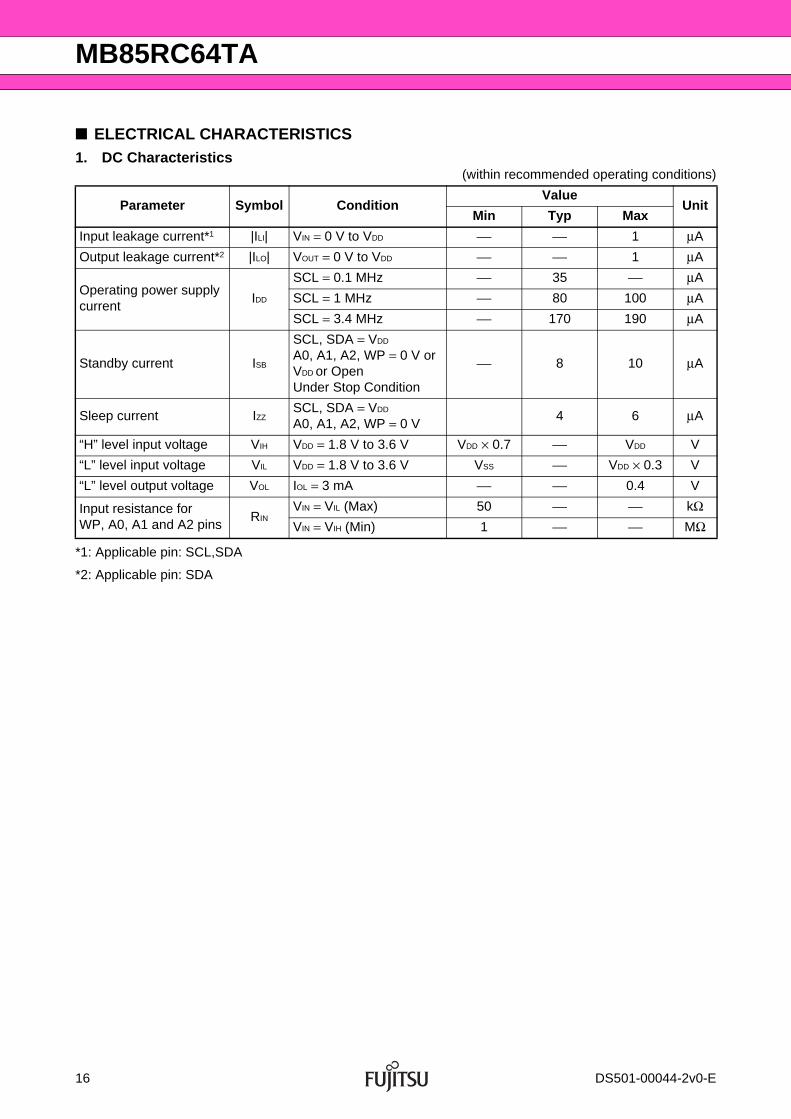
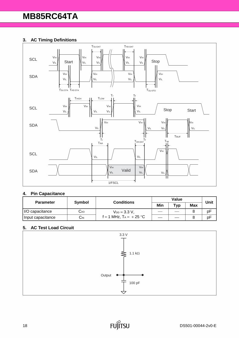
■ ELECTRICAL CHARACTERISTICS1. DC Characteristics
(within recommended operating conditions)
*1: Applicable pin: SCL,SDA
*2: Applicable pin: SDA
Parameter Symbol ConditionValue
UnitMin Typ Max
Input leakage current*1 |ILI| VIN = 0 V to VDD ⎯ ⎯ 1 μA
Output leakage current*2 |ILO| VOUT = 0 V to VDD ⎯ ⎯ 1 μA
Operating power supply current
IDD
SCL = 0.1 MHz ⎯ 35 ⎯ μA
SCL = 1 MHz ⎯ 80 100 μA
SCL = 3.4 MHz ⎯ 170 190 μA
Standby current ISB
SCL, SDA = VDD
A0, A1, A2, WP = 0 V or VDD or OpenUnder Stop Condition
⎯ 8 10 μA
Sleep current IZZSCL, SDA = VDD
A0, A1, A2, WP = 0 V4 6 μA
“H” level input voltage VIH VDD = 1.8 V to 3.6 V VDD × 0.7 ⎯ VDD V
“L” level input voltage VIL VDD = 1.8 V to 3.6 V VSS ⎯ VDD × 0.3 V
I/O capacitance CI/O VDD = 3.3 V, f = 1 MHz, TA = + 25 °C
⎯ ⎯ 8 pF
Input capacitance CIN ⎯ ⎯ 8 pF
Start
StartStop
Stop
Valid
SCL
SDA
SCL
SDA
SCL
SDA
VIH
VIL
VIH
VIL
VIH
VIL
VIH
VIL
VIH
VIL
VIH
VIL
VIH
VIL
VIH
VIL
VIH
VIL
VIH
VIL
VIH
VIL
VIH
VIL
VIH
VIL
VIH
VIL
VIH
VIH VIH
TSU:DAT
TSU:STA THD:STA
THIGH TLOW
TDH:DAT
1/FSCL
TSU:STO
THD:DAT
VIH
VIH
VIH
VIL
VIL
VIL
VIL
VIL
VIL
VIL VIL
TBUFTfTr
TfTr
TAATsp
3.3 V
100 pF
Output
1.1 kΩ
18 DS501-00044-2v0-E
MB85RC64TA
■ POWER ON/OFF SEQUENCE
If the device does not operate within the specified conditions of read cycle, write cycle or power on/offsequence, memory data can not be guaranteed.
■ FRAM CHARACTERISTICS
*1 : Total number of reading and writing defines the minimum value of endurance, as an FRAM memory operates with destructive readout mechanism.
*2 : Minimum values define retention time of the first reading/writing data right after shipment, and these values are calculated by qualification results.
Parameter SymbolValue
UnitMin Max
SDA, SCL level hold time during power down tpd 85 ⎯ ns
SDA, SCL level hold time during power up tpu 250 ⎯ μs
Power supply rising time tr 0.05 ⎯ ms/V
Power supply falling time tf 0.1 ⎯ ms/V
Internal regulator recovery time tREC ⎯ 400 μs
Item Min Max Unit Parameter
Read/Write Endurance*1 1013 ⎯ Times/byte Operation Ambient Temperature TA = + 85 °C
Data Retention*2
10 ⎯
Years
Operation Ambient Temperature TA = + 85 °C
95 ⎯ Operation Ambient Temperature TA = + 55 °C
≥ 200 ⎯ Operation Ambient Temperature TA = + 35 °C
* : SDA, SCL (Max) < VDD + 0.5 V
0 V
SDA, SCL > VDD × 0.8 * SDA, SCL > VDD × 0.8 *
tpd tputrtf
VIL (Max)
VIH (Min)
VDD (Min)
VDD
SDA, SCL : Don't careSDA, SCL SDA, SCL
0 V
VIL (Max)
VIH (Min)
VDD (Min)
VDD
DS501-00044-2v0-E 19
MB85RC64TA
■ NOTE ON USE• We recommend programming of the device after reflow. Data written before reflow cannot be guaranteed. • During the access period from the start condition to the stop condition, keep the level of WP, A0, A1 and
A2 pins to the “H” level or the “L” level.
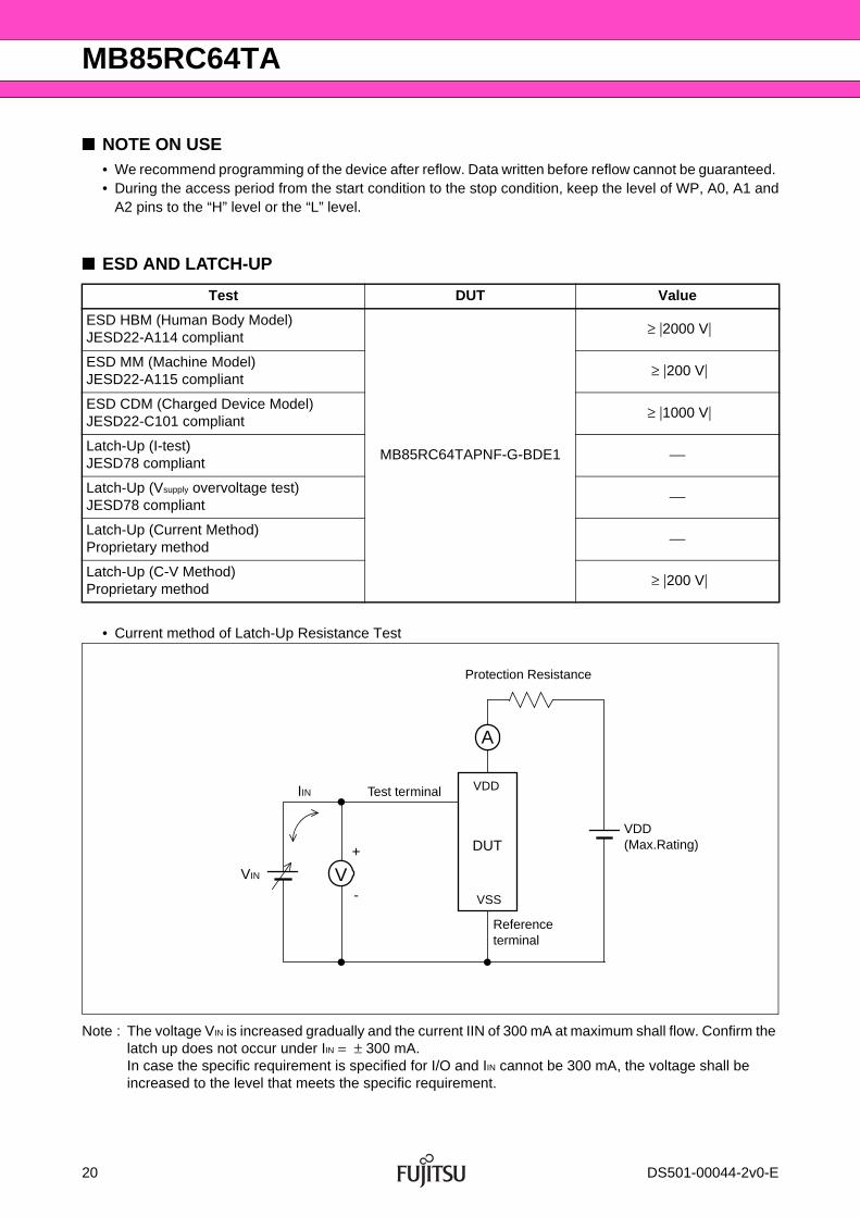
■ ESD AND LATCH-UP
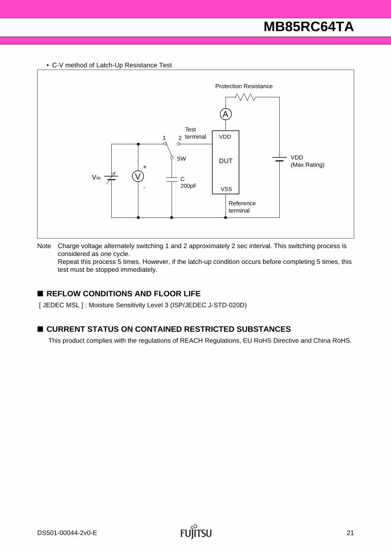
• Current method of Latch-Up Resistance Test
Note : The voltage VIN is increased gradually and the current IIN of 300 mA at maximum shall flow. Confirm the latch up does not occur under IIN = ± 300 mA.In case the specific requirement is specified for I/O and IIN cannot be 300 mA, the voltage shall be increased to the level that meets the specific requirement.
Note Charge voltage alternately switching 1 and 2 approximately 2 sec interval. This switching process is considered as one cycle. Repeat this process 5 times. However, if the latch-up condition occurs before completing 5 times, this test must be stopped immediately.
■ REFLOW CONDITIONS AND FLOOR LIFE [ JEDEC MSL ] : Moisture Sensitivity Level 3 (ISP/JEDEC J-STD-020D)
■ CURRENT STATUS ON CONTAINED RESTRICTED SUBSTANCES This product complies with the regulations of REACH Regulations, EU RoHS Directive and China RoHS.
VDD
VSS
DUT
VIN
+
-
SW
1 2
C200pF
V
A
Test terminal
Protection Resistance
VDD(Max.Rating)
Reference terminal
DS501-00044-2v0-E 21
MB85RC64TA
■ ORDERING INFORMATION
*: Please contact our sales office about minimum shipping quantity.
Part number Package Shipping form Minimum shipping quantity
MB85RC64TAPNF-G-BDE1 8-pin, plastic SOP
(FPT-8P-M09)Tube ⎯*
MB85RC64TAPNF-G-BDERE1 8-pin, plastic SOP
(FPT-8P-M09)Embossed Carrier tape 1500
MB85RC64TAPN-G-AMEWE18-pin, plastic SON
(LCC-8P-M04)Embossed Carrier tape 1500
22 DS501-00044-2v0-E
MB85RC64TA
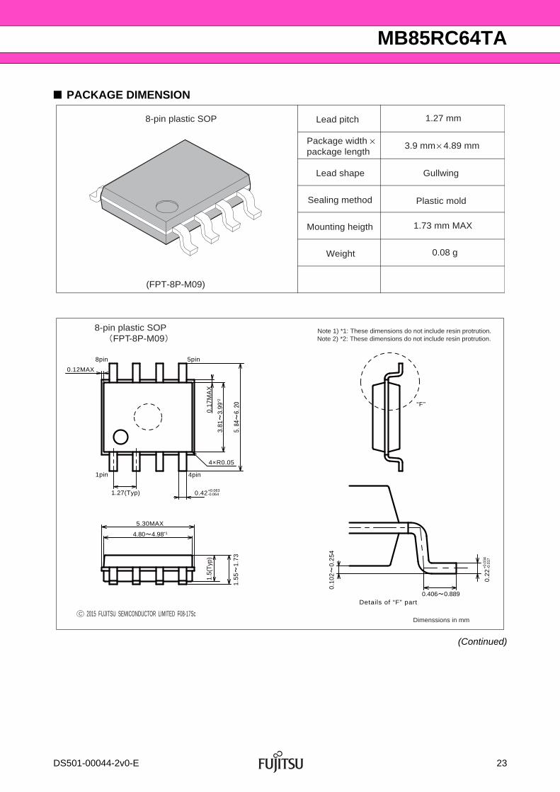
■ PACKAGE DIMENSION
(Continued)
8-pin plastic SOP Lead pitch 1.27 mm
Package width ×package length
3.9 mm× 4.89 mm
Lead shape Gullwing
Sealing method Plastic mold
Mounting heigth 1.73 mm MAX
Weight 0.08 g
8-pin plastic SOPFPT-8P-M09
(FPT-8P-M09)
Note 1) *1: These dimensions do not include resin protrution.
1pin 4pin
5pin8pin
1.5(
Typ
)
4.80 4.98*1
0.10
20.
254
0.406 0.889Deta i ls of “F” part
3.81
3.99
*2
0.17
MA
X
0.12MAX
4×R0.05
5.30MAX
0.22
+0.0
34-0
.017
0.42+0.063-0.0641.27(Typ)
1.55
1.73
C 2015 FUJITSU SEMICONDUCTOR LIMITED F08-17Sc
“F”
Note 2) *2: These dimensions do not include resin protrution.
Dimenssions in mm
DS501-00044-2v0-E 23
MB85RC64TA
(Continued)
8-pin plastic SON Lead pitch 0.5 mm
Package width ×package length
2.0 mm × 3.0 mm
Sealing method Plastic mold
Mounting height 0.75 mm MAX
Weight 0.015g
8-pin plastic SON(LCC-8P-M04)
(LCC-8P-M04)
C 2011 FUJITSU SEMICONDUCTOR LIMITED HMbC8-04Sc-1-1
(.079±.003)2.00±0.07
INDEX AREA
3.00±0.07(.118±.003) (.055±.004)
1.40±0.10
(.010±.002)0.25±0.05
1.6±0.10(.063±.004)
0.05(.002) MAX 0.15(.006)
(.016±.003)0.40±0.07
0.50(.020)
TYP
1PIN CORNER(C0.30(C.012))
(.028±.002)0.70±0.05
Dimensions in mm (inches).Note: The values in parentheses are reference values.
24 DS501-00044-2v0-E
MB85RC64TA
■ MARKING
[MB85RC64TAPNF-G-BDE1][MB85RC64TAPNF-G-BDERE1]
[FPT-8P-M09]
C 6 4 TA1 1 5 4 7
7 0 1
[MB85RC64TAPN-G-AMEWE1]
[LCC-8P-M04]
Y Y W WC64 TA
0XX
DS501-00044-2v0-E 25
MB85RC64TA
■ MAJOR CHANGES IN THIS EDITIONA change on a page is indicated by a vertical line drawn on the left side of that page.
Page Section Change Results
1 ■ FEATURES Added Data retention under 85 °C.
19 ■ FRAM CHARACTERISTICS Added Data retention under 85 °C.
All Rights Reserved.FUJITSU SEMICONDUCTOR LIMITED, its subsidiaries and affiliates (collectively, "FUJITSU SEMICONDUCTOR") reserves the right to make changes to the information contained in this document without notice. Please contact your FUJITSU SEMICONDUCTOR sales representatives before order of FUJITSU SEMICONDUCTOR device. Information contained in this document, such as descriptions of function and application circuit examples is presented solely for reference to examples of operations and uses of FUJITSU SEMICONDUCTOR device. FUJITSU SEMICONDUCTOR disclaimsany and all warranties of any kind, whether express or implied, related to such information, including, without limitation, quality, accuracy, performance, proper operation of the device or non-infringement. If you develop equipment or product incorporating theFUJITSU SEMICONDUCTOR device based on such information, you must assume any responsibility or liability arising out of orin connection with such information or any use thereof. FUJITSU SEMICONDUCTOR assumes no responsibility or liability for anydamages whatsoever arising out of or in connection with such information or any use thereof. Nothing contained in this document shall be construed as granting or conferring any right under any patents, copyrights, or any otherintellectual property rights of FUJITSU SEMICONDUCTOR or any third party by license or otherwise, express or implied. FUJITSU SEMICONDUCTOR assumes no responsibility or liability for any infringement of any intellectual property rights or otherrights of third parties resulting from or in connection with the information contained herein or use thereof. The products described in this document are designed, developed and manufactured as contemplated for general use including without limitation, ordinary industrial use, general office use, personal use, and household use, but are not designed, developed andmanufactured as contemplated (1) for use accompanying fatal risks or dangers that, unless extremely high levels of safety is secured,could lead directly to death, personal injury, severe physical damage or other loss (including, without limitation, use in nuclear facility, aircraft flight control system, air traffic control system, mass transport control system, medical life support system and military application), or (2) for use requiring extremely high level of reliability (including, without limitation, submersible repeaterand artificial satellite). FUJITSU SEMICONDUCTOR shall not be liable for you and/or any third party for any claims or damagesarising out of or in connection with above-mentioned uses of the products. Any semiconductor devices fail or malfunction with some probability. You are responsible for providing adequate designs and safeguards against injury, damage or loss from such failures or malfunctions, by incorporating safety design measures into your facility, equipments and products such as redundancy, fire protection, and prevention of overcurrent levels and other abnormal operating conditions. The products and technical information described in this document are subject to the Foreign Exchange and Foreign Trade ControlLaw of Japan, and may be subject to export or import laws or regulations in U.S. or other countries. You are responsible for ensuringcompliance with such laws and regulations relating to export or re-export of the products and technical information described herein. All company names, brand names and trademarks herein are property of their respective owners.