672 IEEE TRANSACTIONS ON CIRCUITS AND SYSTEMS—I: REGULAR PAPERS, VOL. 55, NO. 2, MARCH 2008
Low-Power VLSI Implementation of the InnerReceiver for OFDM-Based WLAN Systems
Alfonso Troya, Member, IEEE, Koushik Maharatna, Member, IEEE, Milos Krstic, Eckhard Grass,Ulrich Jagdhold, and Rolf Kraemer, Member, IEEE
Abstract—In this paper, we propose low-power designs for thesynchronizer and channel estimator units of the Inner Receiver inwireless local area network systems. The objective of the work isthe optimization, with respect to power, area, and latency, of boththe signal processing algorithms themselves and their implemen-tation. Novel circuit design strategies have been employed to re-alize optimal hardware and power efficient architectures for thefast Fourier transform, arctangent computation unit, numericallycontrolled oscillator, and the decimation filters. The use of multipleclock domains and clock gating reduces the power consumptionfurther. These blocks have been integrated into an experimentaldigital baseband processor for the IEEE 802.11a standard imple-mented in the 0.25- m 5-metal layer BiCMOS technology fromInstitute for High Performance Microelectronics.
Index Terms—Coordinate rotation digital computer (CORDIC),fast Fourier transform (FFT), orthogonal frequency-division mul-tiplexing (OFDM), wireless local area network (WLAN).
I. INTRODUCTION
THE use of the orthogonal frequency division multiplexing(OFDM) technique is currently an active field of research
in the area of communication and has been used to develop wire-less local area network (WLAN) systems, for example the IEEE802.11a/g standards [1], [2]. New standardisation processes al-ready foresee the application of OFDM in future WLAN [3]and ultra-wide-band (UWB) systems [4]. The concept under-lying such a system is to modulate a number of mutually or-thogonal sub-carriers with the input data. This enables the real-ization of high-speed transmission systems. However, the entiresystem performance depends on maintaining the orthogonalityof the sub-carriers and failing to maintain this property results indetrimental effects for example inter-carrier interference (ICI)and inter-symbol interference (ISI) during signal reception. Ina real system, the orthogonality property of the sub-carriers canbe disturbed during the RF up- and down-conversion and by thecharacteristics of the transmission channel.
Manuscript received July 24, 2006; revised December 15, 2006; June 11,2007, and June 24, 2007. This paper was recommended by Associate EditorK. Chakrabarty.
A. Troya was with Institute for High Performance Microelectronics (IHP),Frankfurt (Oder) 15236, Germany. He is now with the European Patent Office,2280-HV Rijswijk, The Netherlands (e-mail: [email protected]).
K. Maharatna was with Institute for High Performance Microelectronics(IHP), Frankfurt (Oder) 15236, Germany. He is now with the ElectronicsSystem Design Group, University of Southampton, Southampton SO17 B1J,U.K. (e-mail: [email protected]).
Digital Object Identifier 10.1109/TCSI.2007.913732
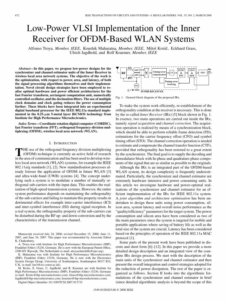
Fig. 1. General block diagram of the proposed IRx.
To make the system work efficiently, re-establishment of theorthogonality condition at the receiver is necessary. This is doneby the so called Inner Receiver (IRx) [5] block shown in Fig. 1.In essence, two main operations are carried out inside the IRx,namely signal acquisition and channel correction. The acquisi-tion operation is realized by means of a synchronization block,which should be able to perform reliable frame detection (FD),estimations for the carrier frequency offset (CFO) and symboltiming offset (STO). The channel correction operation is neededto estimate and compensate the channel transfer function (CTF),provided that orthogonality has been restored to a great extentby the synchronizer. The final goal is to supply the decoding anddemodulator block with In-phase and quadrature-phase compo-nents of the signal that are as similar as possible to the originals.
Although the IRx is an integrated part of the OFDM-basedWLAN system, its design complexity is frequently underesti-mated. Particularly, the synchronizer and channel estimator areextremely hardware intensive and power consuming units. Inthis article we investigate hardware and power-optimal real-izations of the synchronizer and channel estimator for an ef-ficient implementation of the IRx for IEEE 802.11a system.A joint algorithm and architecture optimisation has been un-dertaken to design these units using power consumption, sil-icon area, system latency and overall noise performance as the“quality/efficiency” parameters for the target system. The powerconsumption and silicon area have been considered as two ofthe main parameters since the system is targeted for mobile andportable applications where saving of battery life as well as thetotal size of the system are crucial. Latency has been consideredbased on the principles of operation of the IEEE 802.11a MACprotocol [1].
Some parts of the present work have been published in dis-crete and short form [6]–[12]. In this paper we provide a moredetailed design description and an integrated view of the com-plete IRx design process. We start with the description of themain units of the synchronizer and channel estimator and thenpresent the overall integration and control strategies adopted forthe reduction of power dissipation. The rest of the paper is or-ganized as follows. Section II looks into the algorithmic for-mulations of the synchronizer and channel estimator in brief(since detailed algorithmic analysis is beyond the scope of this
TROYA et al.: LOW-POWER VLSI IMPLEMENTATION OF THE IRX 673
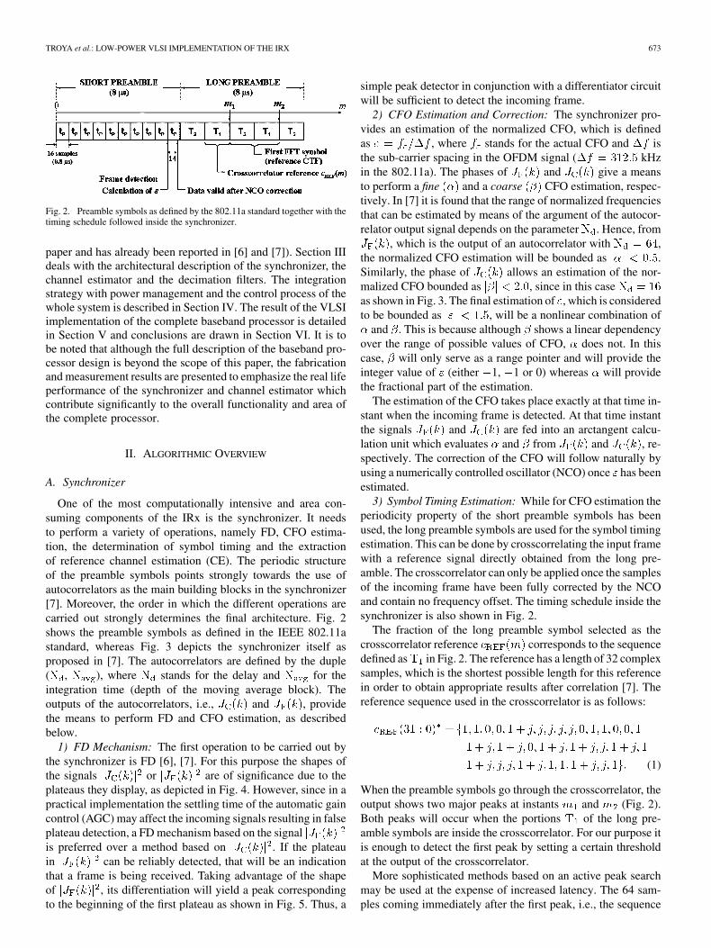
Fig. 2. Preamble symbols as defined by the 802.11a standard together with thetiming schedule followed inside the synchronizer.
paper and has already been reported in [6] and [7]). Section IIIdeals with the architectural description of the synchronizer, thechannel estimator and the decimation filters. The integrationstrategy with power management and the control process of thewhole system is described in Section IV. The result of the VLSIimplementation of the complete baseband processor is detailedin Section V and conclusions are drawn in Section VI. It is tobe noted that although the full description of the baseband pro-cessor design is beyond the scope of this paper, the fabricationand measurement results are presented to emphasize the real lifeperformance of the synchronizer and channel estimator whichcontribute significantly to the overall functionality and area ofthe complete processor.
II. ALGORITHMIC OVERVIEW
A. Synchronizer
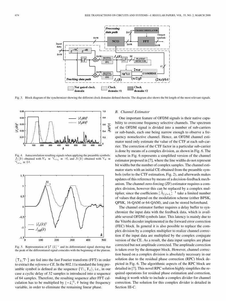
One of the most computationally intensive and area con-suming components of the IRx is the synchronizer. It needsto perform a variety of operations, namely FD, CFO estima-tion, the determination of symbol timing and the extractionof reference channel estimation (CE). The periodic structureof the preamble symbols points strongly towards the use ofautocorrelators as the main building blocks in the synchronizer[7]. Moreover, the order in which the different operations arecarried out strongly determines the final architecture. Fig. 2shows the preamble symbols as defined in the IEEE 802.11astandard, whereas Fig. 3 depicts the synchronizer itself asproposed in [7]. The autocorrelators are defined by the duple( , ), where stands for the delay and for theintegration time (depth of the moving average block). Theoutputs of the autocorrelators, i.e., and , providethe means to perform FD and CFO estimation, as describedbelow.
1) FD Mechanism: The first operation to be carried out bythe synchronizer is FD [6], [7]. For this purpose the shapes ofthe signals or are of significance due to theplateaus they display, as depicted in Fig. 4. However, since in apractical implementation the settling time of the automatic gaincontrol (AGC) may affect the incoming signals resulting in falseplateau detection, a FD mechanism based on the signalis preferred over a method based on . If the plateauin can be reliably detected, that will be an indicationthat a frame is being received. Taking advantage of the shapeof , its differentiation will yield a peak correspondingto the beginning of the first plateau as shown in Fig. 5. Thus, a
simple peak detector in conjunction with a differentiator circuitwill be sufficient to detect the incoming frame.
2) CFO Estimation and Correction: The synchronizer pro-vides an estimation of the normalized CFO, which is definedas , where stands for the actual CFO and isthe sub-carrier spacing in the OFDM signal ( kHzin the 802.11a). The phases of and give a meansto perform a fine and a coarse CFO estimation, respec-tively. In [7] it is found that the range of normalized frequenciesthat can be estimated by means of the argument of the autocor-relator output signal depends on the parameter . Hence, from
, which is the output of an autocorrelator with ,the normalized CFO estimation will be bounded as .Similarly, the phase of allows an estimation of the nor-malized CFO bounded as , since in this caseas shown in Fig. 3. The final estimation of , which is consideredto be bounded as , will be a nonlinear combination of
and . This is because although shows a linear dependencyover the range of possible values of CFO, does not. In thiscase, will only serve as a range pointer and will provide theinteger value of (either 1, 1 or 0) whereas will providethe fractional part of the estimation.
The estimation of the CFO takes place exactly at that time in-stant when the incoming frame is detected. At that time instantthe signals and are fed into an arctangent calcu-lation unit which evaluates and from and , re-spectively. The correction of the CFO will follow naturally byusing a numerically controlled oscillator (NCO) once has beenestimated.
3) Symbol Timing Estimation: While for CFO estimation theperiodicity property of the short preamble symbols has beenused, the long preamble symbols are used for the symbol timingestimation. This can be done by crosscorrelating the input framewith a reference signal directly obtained from the long pre-amble. The crosscorrelator can only be applied once the samplesof the incoming frame have been fully corrected by the NCOand contain no frequency offset. The timing schedule inside thesynchronizer is also shown in Fig. 2.
The fraction of the long preamble symbol selected as thecrosscorrelator reference corresponds to the sequencedefined as in Fig. 2. The reference has a length of 32 complexsamples, which is the shortest possible length for this referencein order to obtain appropriate results after correlation [7]. Thereference sequence used in the crosscorrelator is as follows:
(1)
When the preamble symbols go through the crosscorrelator, theoutput shows two major peaks at instants and (Fig. 2).Both peaks will occur when the portions of the long pre-amble symbols are inside the crosscorrelator. For our purpose itis enough to detect the first peak by setting a certain thresholdat the output of the crosscorrelator.
More sophisticated methods based on an active peak searchmay be used at the expense of increased latency. The 64 sam-ples coming immediately after the first peak, i.e., the sequence
674 IEEE TRANSACTIONS ON CIRCUITS AND SYSTEMS—I: REGULAR PAPERS, VOL. 55, NO. 2, MARCH 2008
Fig. 3. Block diagram of the synchronizer showing the different clock domains defined therein. The diagram also shows the bit length of the most relevant signals.
Fig. 4. Autocorrelation resulting signals when applying the preamble symbols:J (k) obtained with N = N = 16, and J (k) obtained with N =N = 64.
Fig. 5. Representation of jJ (k)j and its differentiated signal showing thatthe peak of the differentiated signal coincides with the beginning of the plateau.
are fed into the fast Fourier transform (FFT) in orderto extract the reference CE. In the 802.11a standard the long pre-amble symbol is defined as the sequence , i.e., in ourcase a cyclic delay of 32 samples is introduced into a sequenceof 64 samples. Therefore, the resulting sequence after FFT cal-culation has to be multiplied by , being the frequencyvariable, in order to eliminate the remaining linear phase.
B. Channel Estimator
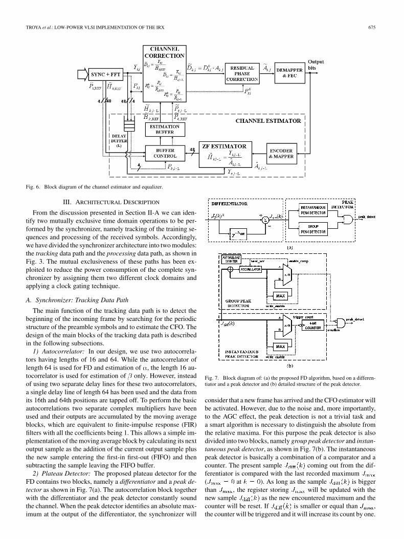
One important feature of OFDM signals is their native capa-bility to overcome frequency selective channels. The spectrumof the OFDM signal is divided into a number of sub-carriersor sub-bands, each one being narrow enough to observe a fre-quency nonselective channel. Hence, an OFDM channel esti-mator need only estimate the value of the CTF at each sub-car-rier. The correction of the CTF factor in a particular sub-carrieris done by means of a complex division, as shown in Fig. 6. Thescheme in Fig. 6 represents a simplified version of the channelestimator proposed in [7], where the line widths do not representbit widths but the number of complex samples. The channel esti-mator starts with an initial CE obtained from the preamble sym-bols (refer to the CTF estimation, Fig. 2), and afterwards makesupdates of this reference by means of a decision-feedback mech-anism. The channel zero-forcing (ZF) estimator requires a com-plex division, however this can be replaced by a complex mul-tiplier, since the coefficients take a limited numberof values that depend on the modulation scheme (either BPSK,QPSK, 16-QAM or 64-QAM), and can be stored beforehand.
The channel estimator further requires a delay buffer to syn-chronize the input data with the feedback data, which is avail-able several OFDM symbols later. This latency is mainly due tothe Viterbi decoder implemented in the forward error correction(FEC) block. In general it is also possible to replace the com-plex division by a complex multiplier to realize channel correc-tion if the input data are multiplied by the complex conjugateversion of the CE. As a result, the data input samples are phasecorrected but not amplitude corrected. The amplitude correctionis taken over by the demapper block. However, channel correc-tion based on a complex division is absolutely necessary in oursolution due to the residual phase correction (RPC) block de-picted in Fig. 6. The algorithmic aspects of the RPC block aredetailed in [7]. This novel RPC solution highly simplifies the re-quired operations for residual phase estimation and correction,making it worth while to include a complex divider for channelcorrection. The solution for this complex divider is detailed inSection III-C.
TROYA et al.: LOW-POWER VLSI IMPLEMENTATION OF THE IRX 675
Fig. 6. Block diagram of the channel estimator and equalizer.
III. ARCHITECTURAL DESCRIPTION
From the discussion presented in Section II-A we can iden-tify two mutually exclusive time domain operations to be per-formed by the synchronizer, namely tracking of the training se-quences and processing of the received symbols. Accordingly,we have divided the synchronizer architecture into two modules:the tracking data path and the processing data path, as shown inFig. 3. The mutual exclusiveness of these paths has been ex-ploited to reduce the power consumption of the complete syn-chronizer by assigning them two different clock domains andapplying a clock gating technique.
A. Synchronizer: Tracking Data Path
The main function of the tracking data path is to detect thebeginning of the incoming frame by searching for the periodicstructure of the preamble symbols and to estimate the CFO. Thedesign of the main blocks of the tracking data path is describedin the following subsections.
1) Autocorrelator: In our design, we use two autocorrela-tors having lengths of 16 and 64. While the autocorrelator oflength 64 is used for FD and estimation of , the length 16 au-tocorrelator is used for estimation of only. However, insteadof using two separate delay lines for these two autocorrelators,a single delay line of length 64 has been used and the data fromits 16th and 64th positions are tapped off. To perform the basicautocorrelations two separate complex multipliers have beenused and their outputs are accumulated by the moving averageblocks, which are equivalent to finite-impulse response (FIR)filters with all the coefficients being 1. This allows a simple im-plementation of the moving average block by calculating its nextoutput sample as the addition of the current output sample plusthe new sample entering the first-in first-out (FIFO) and thensubtracting the sample leaving the FIFO buffer.
2) Plateau Detector: The proposed plateau detector for theFD contains two blocks, namely a differentiator and a peak de-tector as shown in Fig. 7(a). The autocorrelation block togetherwith the differentiator and the peak detector constantly soundthe channel. When the peak detector identifies an absolute max-imum at the output of the differentiator, the synchronizer will
Fig. 7. Block diagram of: (a) the proposed FD algorithm, based on a differen-tiator and a peak detector and (b) detailed structure of the peak detector.
consider that a new frame has arrived and the CFO estimator willbe activated. However, due to the noise and, more importantly,to the AGC effect, the peak detection is not a trivial task anda smart algorithm is necessary to distinguish the absolute fromthe relative maxima. For this purpose the peak detector is alsodivided into two blocks, namely group peak detector and instan-taneous peak detector, as shown in Fig. 7(b). The instantaneouspeak detector is basically a combination of a comparator and acounter. The present sample coming out from the dif-ferentiator is compared with the last recorded maximum( at ). As long as the sample is biggerthan , the register storing will be updated with thenew sample as the new encountered maximum and thecounter will be reset. If is smaller or equal than ,the counter will be triggered and it will increase its count by one.
676 IEEE TRANSACTIONS ON CIRCUITS AND SYSTEMS—I: REGULAR PAPERS, VOL. 55, NO. 2, MARCH 2008
If this situation persists until the counter overflows, the instan-taneous peak detector will activate a signal stating that a relativepeak has been found inside the counting scope of the counter.On the other hand, the group peak detector is used to detect thefalling edges in , and its main component is also a com-parator circuit. Here, the input signal is accumulated in groupsof six samples and the average value of the present group is com-pared with the previous one. If the value for the present groupis smaller than the one stored from the previous group, then itcan be interpreted as the starting point of the falling slope. Ifthe group peak detector finds a falling slope at the same time asthe instantaneous peak detector finds a relative peak, then thedetected peak is actually an absolute peak and accordingly thedetected frame is acquired by asserting the signal peak_detectshown in Fig. 7.
The influence of noise in the FD algorithm is mitigated by ap-plying a threshold to the signal prior to plateau detec-tion. At the time instant when the peak_detect becomes active,the sample from at that particular time instant is stored ina register and the arctangent calculator is activated. On the nextclock cycle the signal is also input to the arctangentcalculator.
3) Arctangent Computation Unit: The arctangent compu-tation unit computes the phase angles of the complex signals
and to generate the values of and , respectively.In practice, it outputs the values of and since thearctangent computation is bounded in the range and
, . Evaluation of arctangents is a nontrivialand computationally intensive task. For this purpose the coor-dinate rotation digital computer (CORDIC) algorithm has beenused in its vectoring mode of operation in circular coordinates[13]. The most attractive point about CORDIC is that it requiresonly shift-and-add operations and thus the resulting hardware isvery economical. However, the main limitations of the classicalCORDIC approach are twofold: slow operation speed and thegeneration of a bulk scale factor, whose compensation requiresextra circuitry and processing time, yet it should be noted thatthe scale factor compensation is not necessary in the evaluationof arctangent.
In [9], we have developed a virtually scaling-free CORDICalgorithm that eliminates the requirement of the scale factorcompensation step, speeds up the CORDIC operation by adap-tively executing only the required iterations and exhibits guar-anteed convergence over the entire coordinate space. In thisformulation it is considered a one-sided vector rotation onlyas opposed to the classical CORDIC, which approximates thetarget angle/final vector through to-and-fro vector rotation. Theoperation of the scaling-free CORDIC can be described by thefollowing equation set [9]:
(2)
where and are the components of the final output vector,is the accumulated angle up to the th iteration,
, is the wordlength, and rounds to the nearestinteger towards minus infinity.
The basic idea for designing a virtually scaling-free CORDICprocessor lies in extending the convergence range of the scaling-free CORDIC algorithm given by (2), which originally has alimited range of convergence, by applying a technique knownas domain folding. Using domain folding we have shown thatthe result of the CORDIC operation with any target angle/vector(for rotation/vectoring operation) lying in the coordinate spacecan be computed by first mapping the angle/vector to a range
and then executing the CORDIC operation on it. Fig. 8shows a flowchart of the virtually scaling-free CORDIC algo-rithm operating in the vectoring mode. The complete theoreticalformulation and performance results can be found in [9] and areomitted here for conciseness.
It is pretty straightforward to map the algorithm to hardware.However, from an implementation point of view, further opti-mization can be done by exploiting one sided vector rotation inthe virtually scaling-free CORDIC framework.
Rotating the vector in one direction only essentially meansthat the accumulated angle can be described as a pure summa-tion of powers of two. In this process, the iteration steps not ac-tually needed are skipped. The final accumulated angle can bedescribed by a bit pattern that contains logic “1” correspondingto the required iteration steps and logic “0” corresponding to thenot required iterations. In essence, this technique eliminates allthe unnecessary addition/subtraction operations along the angleaccumulation datapath and reduces the hardware cost dras-tically. This process is described by the flow chart in Fig. 8.
An implementation of this algorithm is described in detail in[10]. However, in this particular work we need only the arct-angent computation part of the complete vectoring CORDIC.The arctangent computation unit consists of three modules viz.the domain detection circuit, the basic CORDIC section, andthe output unit as shown in Fig. 9(a). An analysis of the targetspecification shows that a 16-bit arctangent computation unit issufficient for our purpose. Two’s complement arithmetic is usedthroughout the implementation.
The domain detection circuit is responsible for detecting theappropriate quadrant and the corresponding domain in whichthe vector lays. It consists of two comparators, two adders anda scaling unit of . The scaling circuit is realized using ashift-and-add technique and thus it is more economical than afull multiplier. It generates two 2-bit signals, namely quad anddomain. While the quad signal indicates the initial quadrant inwhich the vector lays, the domain signal indicates the domain inthe first quadrant from where the vector has been mapped. Theentire operation requires one clock cycle.
The basic data path unit (called elementary rotationalunit) used for constructing the CORDIC pipeline is shownin Fig. 9(b), where is the iteration index. It consists of fourshifters and four adder/subtracters. For the pipelined imple-mentation the shifters get reduced to only the wire connectionsand thus, the effective hardware complexity of the elementaryrotational unit becomes equal to four adder/subtracters only.However, for a 16-bit implementation and for the hard-ware complexity of the basic rotational unit becomes equal totwo adder/subtracters since a right shift by 15-bits only resultsin retention of the sign bit. Each of these basic data path unitsis also equipped with a signal which is asserted when the
TROYA et al.: LOW-POWER VLSI IMPLEMENTATION OF THE IRX 677
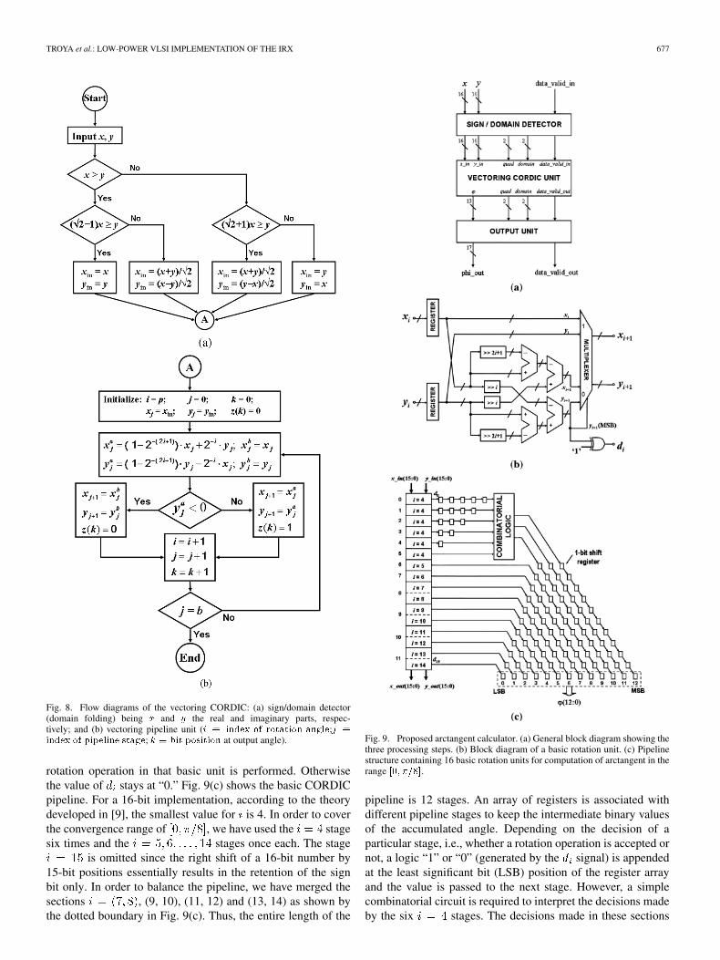
Fig. 8. Flow diagrams of the vectoring CORDIC: (a) sign/domain detector(domain folding) being x and y the real and imaginary parts, respec-tively; and (b) vectoring pipeline unit (i � index of rotation angle;j �index of pipeline stage; k � bit position at output angle).
rotation operation in that basic unit is performed. Otherwisethe value of stays at “0.” Fig. 9(c) shows the basic CORDICpipeline. For a 16-bit implementation, according to the theorydeveloped in [9], the smallest value for is 4. In order to coverthe convergence range of , we have used the stagesix times and the stages once each. The stage
is omitted since the right shift of a 16-bit number by15-bit positions essentially results in the retention of the signbit only. In order to balance the pipeline, we have merged thesections , (9, 10), (11, 12) and (13, 14) as shown bythe dotted boundary in Fig. 9(c). Thus, the entire length of the
Fig. 9. Proposed arctangent calculator. (a) General block diagram showing thethree processing steps. (b) Block diagram of a basic rotation unit. (c) Pipelinestructure containing 16 basic rotation units for computation of arctangent in therange [0; �=8].
pipeline is 12 stages. An array of registers is associated withdifferent pipeline stages to keep the intermediate binary valuesof the accumulated angle. Depending on the decision of aparticular stage, i.e., whether a rotation operation is accepted ornot, a logic “1” or “0” (generated by the signal) is appendedat the least significant bit (LSB) position of the register arrayand the value is passed to the next stage. However, a simplecombinatorial circuit is required to interpret the decisions madeby the six stages. The decisions made in these sections
678 IEEE TRANSACTIONS ON CIRCUITS AND SYSTEMS—I: REGULAR PAPERS, VOL. 55, NO. 2, MARCH 2008
give the three most significant bits (MSBs) of the final represen-tation of the accumulated angle. At the end, the basic CORDICpipeline generates a 13-bit unsigned value for the accumulatedangle which can be further processed by the output unit.
The data and the information about the quadrant (signal quad)and domain (signal domain) shown in Fig. 9(a) of the initialvector detected in the domain detection circuitry are transferredsynchronously between two successive sections of the pipelinein a local register transfer manner. This means that each of thedata in different sections of the pipeline has a token attributedto it that carries the information about the initial quadrant anddomain of that particular data (not shown in Fig. 9(c)), which isused by the output unit to generate the final result.
The main hardware of the output unit consists of one adderand some registers. Depending on the domain and quad signals,it generates the final phase angle by addition/subtraction of theaccumulated angle to/from or in accordance with thetheory developed in [9]. At the same time it asserts an outputenable signal for two cycles to indicate to the Combine blockthat valid data are now present at its input. All the operations inthis unit are performed in one clock cycle.
The entire architecture exhibits a latency of 14 clock cycles.The total hardware complexity of the arctangent unit is 816 fulladders and 553 registers. A big advantage of this design is thatit completely eliminates all the arithmetic operations associ-ated with the angle accumulation data path of a conventionalCORDIC implementation. This results in about 35% saving interms of registers although the required number of adders isslightly more than that of the classical CORDIC implementa-tion when used for computing the arctangent function only.
4) Combine Unit: The combine unit is responsible for thenonlinear combination of and (or strictly speaking and
to generate the estimated normalized CFO . Itconsists of four 17-bit comparators, some logic circuitry with asmall number of logic gates, two adder/subtractors and a multi-plexer. The comparators are required for comparing the valuesof with and . The conditionsor are determined by checking the most significantbit of . The adder/subtractors compute the termsand in parallel and these are fed into the multi-plexer along with . The output from the logic circuitry actsas the select line of this multiplexer, choosing the appropriatevalue for . However, the input data to the NCO needs to be
, which is represented using 17 bits and is obtained byshifting the value of by six bit positions to the right. Thisvalue is stored in the NCO register when the signal rot_val_okis asserted by the combine unit. Note that no sign inversion of
is required since the results provided by the arctan-gent calculator already contain the correct sign information forfrequency correction.
B. Synchronizer: Processing Data Path
Activity of the processing data path starts when the signalrot_val_ok is asserted by the combine unit. This part of the syn-chronizer performs the carrier frequency error correction, esti-mates the symbol timing and obtains the reference CE. It con-sists mainly of the NCO, the 64-point FFT and the crosscorre-
lator. The designs of the NCO and the FFT blocks are describedin the following subsections.
1) NCO: The main task of the NCO is to multiply the thinput data by , where . A natural choice forcarrying out such an operation is a complex multiplier with alook-up table (ROM memory) where the pre-computed valuesof one period of the sine and cosine functions are stored. Thissolution is also known as direct digital synthesis (DDS), and itsmain drawback is the size of the ROM memories. Hence, eachmemory position contains the phase value ,
, where is the number of addressing bits, i.e., thephase increment between two memory positions equals .In our case the phase increment is given by ,resulting in the design condition . The arctangentcalculator has been designed to provide a minimum value of
, which results in . Since each sample ofthe sine/cosine functions is represented with 16 bits, the totalmemory requirement of the DDS solution is 32 KB. Obviouslythe memory requirement could be reduced to the half if thesine/cosine functions were obtained by addressing one singlememory, but this would double the required clock frequency andincrease the control burden. On the contrary, the CORDIC algo-rithm in its rotational mode of operation in circular coordinateoffers a flexible and hardware efficient realization of the NCO[13]. To design the NCO we have used once again the virtuallyscaling-free adaptive CORDIC method developed in [9]. Thetheoretical details of this unit, including the data for numericalaccuracy and hardware comparison with similar kind of proces-sors, can be found in [11], and is not provided here due to spacerestrictions. However, for the sake of completeness we presenta brief description of it subsequently.
The general structure of the NCO is nearly the same as thatfor the arctangent computation unit. It consists of three mod-ules namely, the domain detection circuitry, the basic CORDICpipeline and the output unit. However, although the basicCORDIC pipeline of the NCO and the arctangent computationunit are the same, there are some subtle differences owing tothe fact that while the arctangent unit computes the phase angle,the NCO actually rotates the input vector by a target angle. Forimplementation of the NCO we have selected a binary two’scomplement fixed-point representation and the decimal 1 isrepresented as 00100000000000000. Now, once again, becauseof the domain folding [9], all the angles lying in the coordinatespace are effectively mapped into the range . Thus,the effective maximum target angle that has to be computedis . Using the definition of decimal 1stated above, this angle can be represented in binary formatas 00001100100100001 with an error of . Thus, fromthe implementation point of view, by representing the absolutevalue of any angle lying in this modified convergence rangeone can omit the first 4 MSBs and use the 13 LSBs. In ourarchitecture we use this fact to reduce the total computation inthe angle approximation data path.
The domain detection circuitry has two 16-bit wide datawords for the two primary inputs (the real and imaginary partof the input data respectively) and a 17-bit data word for thetarget angle. In our implementation we have assumed that thetarget angle lies in the range and thus it can be rep-
TROYA et al.: LOW-POWER VLSI IMPLEMENTATION OF THE IRX 679
resented by 17 bits. The principal task of the domain detectioncircuitry is to detect the sign and domain of the target angle andsubsequently, it applies the domain folding technique to derivethe 13-bit unsigned representation of the modified target angle
. Like the arctangent computation unit, it also generates two2-bit signals, namely domain and quad which have identicalfunctionality of the domain and quad signals of the arctangentcomputation unit. The entire operation in this unit is performedin one clock cycle.
The domain detection unit needs two 16-bit adders and twocomparators. However, in both comparators one of the inputvariables is constant. The hardware complexity of each of thesecomparators is estimated conservatively as equivalent to one4-bit adder.
As mentioned earlier, the basic CORDIC pipeline of the NCOuses an elementary rotational unit (shown in Fig. 9(b), withoutthe circuitry for signal) similar to the one employed in the arc-tangent unit. Since we use one-sided vector rotation only [9],[11] the target angle is approximated as a pure summation of
. As a result, the appropriate elementary rotational sectionsto be selected for a particular target angle have a one-to-onecorrespondence with the position of a logic “1” in the 13-bitunsigned representation of . As an example, let us consider
(0.349 radian): The binary unsigned representation ofthis angle is 1011001010111. To achieve this target angle, therotational sections that have to be activated are , 4, 4, 4, 4,5, 8, 10, 12, 13, and 14. The three MSBs of are used to decidethe number of active stages with . In the present examplethese bits are . The deactivated elementary rotationalsections (corresponding to the bit positions having logic “0”)are bypassed. This implies a significant reduction of arithmeticcomputations that results in a reduction of power consumption.It is to be noted that as the range of is , under no con-dition a logic “1” can arise at twelfth-, eleventh-, and tenth-bitposition of the unsigned representation of simultaneously. Tokeep the pipeline operation intact, we feed the individual bits ofthe 13-bit unsigned representation of to the appropriate ele-mentary rotational sections as an enable signal for that partic-ular section through an array of single bit shift registers. Thenumber of the shift registers corresponding to each section ischosen in such a manner that the appropriate section gets en-abled at the correct clock cycle. To generate the enable signalsfor the six sections, we need a simple logic combina-tion of the twelfth, eleventh, and tenth bit. For the other elemen-tary rotational sections the respective bits can be fed directly tothe 0th shift register of the corresponding shift register array.This arrangement essentially mimics the procedure for adap-tive selection of the elementary rotational stages described in [9]and eliminates the attendant hardware for the angle approxima-tion data path completely. The structure of the basic pipelinedCORDIC processor using this arrangement is shown in Fig. 10.Here the solid lines indicate the boundary of each of the ele-mentary rotational sections whereas the dotted lines indicate theconcatenated elementary rotational stages.
The last unit of the NCO block is the output unit. This circuitconsists of two fixed scaling units of and two adder/sub-tracter units. Each of the scaling units is realized using five16-bit adders. Thus, the overall hardware complexity of this
Fig. 10. Basic pipelined structure of the proposed NCO.
unit is equivalent to twelve 16-bit adders. Depending on the do-main and quad signals this unit assigns the sign, applies eithera scaling of or simply passes the output vector emergingfrom the pipelined CORDIC to the primary output. All the op-erations in the output unit are completed in one clock cycle.
The total hardware cost associated with the NCO is equiv-alent to 768 full adders and 533 registers. Although the hard-ware complexity of the basic CORDIC pipeline is the same forboth the arctangent computation unit and the NCO, the maindifference comes from the domain detection and output units.Compared to the hardware cost of the conventional CORDICprocessor with scaling circuitry, the design requires 22% lessadders and 53% less registers, and on average 50% less compu-tation to converge to the target angle [9], [11]. The significantsaving in hardware as well as the number of computations re-duces the power consumption of the design.
2) Symbol Timing Estimator: The processing task followingthe frequency offset correction is the symbol timing estimation.As has been discussed in Section II, this has been performedusing the long preamble symbol and crosscorrelator. Thecrosscorrelator compares the input symbols with the referencesymbol given in (1). However, from an implementation point ofview, the complex crosscorrelator is a very hardware and powerconsuming component since it requires complex multiplicationoperations. To alleviate this problem we have used a simplifiedscheme for the crosscorrelator based on simple 1-bit XNOR
multipliers. The basic multiplier cell used here is shown inFig. 11(a). In this scheme instead of multiplying -bit complexnumbers, the XNOR multiplier only performs multiplication ofthe sign bit of the complex input values and assigns “1” whenthis value is positive and “0” otherwise. A further simplificationof this structure is possible if one of the inputs is fixed andknown beforehand. In this simplification the XNOR gates can bereplaced by inverters resulting into smaller silicon area.
The overall structure of the crosscorrelator is shown inFig. 11(b). The structure of each of the multiplier cells isdecided upon the reference signal (given by(1)), where it has already been explained that the reference iscomplex conjugated, hard-limited and order-reversed.
680 IEEE TRANSACTIONS ON CIRCUITS AND SYSTEMS—I: REGULAR PAPERS, VOL. 55, NO. 2, MARCH 2008
Fig. 11. Block diagram of: (a) sign-bit complex multiplier and (b) crosscorre-lator with indication of bit lengths.
As discussed in Section II, the result of this crosscorrelationshows two major peaks at the instants and in Fig. 2. Forour purpose it is sufficient to detect the first peak by setting athreshold value at the output of the crosscorrelator. A single realmultiplier is used to compute the square of the absolute magni-tude of the complex signal emerging from the crosscorrelatoroutput. This value is compared with the predefined thresholdvalue for detecting the occurrence of the first peak. The 64 in-coming samples immediately after the first peak are fed intothe FFT processor for the reference CE, which is used by thechannel correction block.
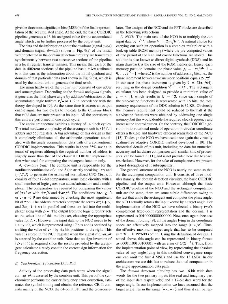
3) FFT Processor: The third part of the processing data pathis the FFT processor. The 64 data samples coming after thesymbol timing detection are used as its input. However, beforeFFT operation, the data symbols go through a cyclic prefix ex-traction block since for every data symbol, 80 samples are ex-pected but only the last 64 are fed to the FFT block. Accordingto the 802.11a standard [1], a 64-point FFT [or inverse FFT(IFFT)] computation has to be performed in 4 s. As discussedin [12] a radix-2 butterfly algorithm is not a good choice forachieving the required speed. Radix-4 FFT formulation has thepotential to satisfy the speed but a radix-8 reformulation of the64-point FFT gives some advantages in terms of power and sil-icon area. A particularly important feature for radix-8 formula-tion is the reduction of the number of nontrivial complex mul-tiplications. This can be achieved by considering the fact thatthe twiddle factors for the first two columns of a decimation intime (DIT) 8-point FFT flow graph are either 1 or whereasthe twiddle factors required for the third column can be easilyrealized using only a shift-and-add principle. Considering thiswe have selected a radix-8 implementation of the 64-point FFT.
Fig. 12. Block diagram of the 64-point FFT/IFFT processor.
The detailed design of the FFT/IFFT processor can be foundin [12]. Here we provide a brief overview of the design forcompleteness.
As discussed in [12], the 64-point FFT can be computed byperforming two 8-point FFTs. Here every eighth sample of theinput data set forms a data subset that undergoes 8-point FFTcomputation. The result of the first 8-point FFT has to be multi-plied by the corresponding inter-dimensional coefficientsbefore the computation of the second 8-point FFT. In this for-mulation 49 nontrivial complex multiplications are needed for a64-point FFT computation [12]. These can be performed usingonly eight pairs of unique nontrivial twiddle factors and thusless storage space is required for the twiddle factors comparedto the other algorithms.
The block diagram of the FFT processor is shown in Fig. 12.It consists of an input buffer of size 56 16 bits, two 8-pointFFT units, one multiplier unit, one internal storage buffer ofsize 64 16 bits and an output buffer of size 56 16 bits.The incoming data samples are fed into the input buffer in a se-rial manner and the outputs are tapped off from the positions
where , which serve as the inputs to thefirst 8-point FFT. At every clock cycle the data at position ofthe input buffer is shifted to the position , ranging from1 to 56. Thus, after 56 cycles (when the buffer is full) the ap-propriate data becomes self-aligned with the inputs of the first8-point FFT. This arrangement substantially reduces the numberof globally multiplexed wires. Owing to the reduced complexityof the 8-point FFT we have realized it in a fully parallel mannerand thereby perform the 8-point FFT in one clock cycle. Thedata coming out from the first 8-point FFT are then fed into themultiplication unit where they are multiplied by eight pairs oftwiddle factors. To save area and power, we have utilized theshift-and-add principle for doing the multiplication operationand thus each of the twiddle factors reduces to a hard-wired con-nection of adders [12]. Eight such hard-wired twiddle factorsare placed in parallel and hence eight complex multiplicationsare carried out in one single clock cycle. The resulting data arestored in an intermediate buffer from where they are fed intothe second 8-point FFT unit. To reduce the number of globallymultiplexed wires an approach similar to the input buffer (down-ward shifting of data at every clock cycle) has been adopted.The data coming out from the second 8-point FFT are fed atthe positions, , of the output buffer and thedata residing in the buffer are shifted downwards by one po-sition at every clock cycle to generate the serial output in thecorrect order.
Although it is possible to use a serial architecture for the mul-tiplier unit, we have avoided it for two reasons: Firstly, using aserial architecture incurs significantly more global wiring since
TROYA et al.: LOW-POWER VLSI IMPLEMENTATION OF THE IRX 681
each output of the 8-point FFT (16-bit complex data) has to bemultiplexed at the input of the multiplier unit. There are signifi-cant routing overheads involved in this. Secondly, if a complexmultiplier is used with a small RAM to store the values of thetwiddle factors, then, in order to maintain the timing, it needs tobe run at a frequency eight times higher than the base frequency(20 MHz). This leads to high power dissipation as well as com-plex multiple-frequency design. On top of this, since data comefrom the 8-point FFT in parallel, one needs to keep a buffer tohold the data set, which once again consumes significant area.Alternatively, a serial 8-point FFT architecture may be used witha complex multiplier. Although it eliminates the requirement ofbuffering, it would increase the data multiplexing, and henceglobal routing, at the input of the 8-point FFT enormously. Inaddition, in order to meet the timing specification, the entireprocessor would need to operate at a much higher clock fre-quency than 20 MHz, which once again would result in highpower dissipation.
To control the entire operation we have used a 5-bit mastercontrol counter; the operations of the different parts of the archi-tecture are synchronized with the count number. On the otherhand, two separate 6-bit counters have been used for control-ling the input and output unit. The overall FFT block can beenabled by asserting a signal data_valid_in. The input controlcounter gets incremented at every clock cycle to track the datainput phase. Once the 56th datum is entered, the input controlcounter enables the master control counter and from then onthe operations are controlled by the master counter. Similarly,on availability of the first output data set to the output buffer,the master counter enables the output counter, which then con-trols the data movement in the output buffer. Upon activationthe output counter also asserts the signal data_valid_out to in-dicate that the valid data is now available at the output.
This architecture performs the parallel-to-parallel FFT in 23clock cycles and thus a clock rate of 20 MHz is sufficient tosatisfy the timing requirements.
A detailed performance comparison of this processor withsome other existing 64-point FFT processors is made in [12]considering the number of cycles, silicon area and power con-sumption. The comparison shows that this processor offers sig-nificant advantages in all the three areas. These performanceparameters are omitted from this paper; interested readers arereferred to [12] for a detailed analysis.
The last operation in the processing data path is channel re-ordering. After FFT computation, the output is arranged in nat-ural order, which needs to be changed for further processing.This is done in the output buffer of the FFT processor itselfby a simple hard-wired mapping of the data emerging from thesecond 8-point FFT to the output register.
C. Channel Correction
As described earlier, the chosen method for CE is based ona decision-directed approach, in which the demodulated bits(output from the Viterbi decoder) are used by the algorithm asa reference to perform the CE. The CE block requires a numberof buffers to compensate for the latency of the Viterbi decoder.This latency comes from the fact that the CE algorithm works
on a symbol basis whereas the number of bits transmitted oneach symbol varies according to the transmission rate. The pro-cessing latency of the channel estimator block in the forwarddirection is fixed (650 ns) but the loop latency varies due to thedifferent processing times required by the Viterbi decoder fordifferent data rates. The loop delay (the time elapsed betweenthe data being available at the output of the channel estimatorand the coded information for the same symbol appearing at theoutput of the feedback loop) varies between 11.3 s (54 Mbps)to 15.05 s (6 Mbps.) This means that the CE needs to buffer upto four OFDM symbols in the worst case. Nevertheless, the loopdelay does not affect the MAC layer, but the processing latency,i.e., 650 ns.
A key component in the CE is the complex divider. The divi-sion of two complex values andresults in with
(3)
Nevertheless, the following simplification of (3) is possible:
(4)
In (4) the values and have a common element, which has to be calculated only once. Comparing (3) with
(4) shows that the latter requires three more addition operationsthan the former, but at the same time it saves one multiplicationoperation, which comparatively is much more computationallyintensive than the three adders. However, two real division op-erations are to be performed as explained next.
The realization of the real dividers is based on a pipelined im-plementation of the linear CORDIC algorithm, where the rela-tionship between the input and the output vectors may be writtenas follows [13]:
(5)
Again, the CORDIC algorithm is used in vectoring mode byaccumulating only the necessary rotations until the condition
is reached (or at least becomes a machine zero.)From (5) it is readily seen that in this case .
In our implementation it is considered that both andare always positive variables. The input stage to the dividershould ensure this condition and provide the sign informationin the form of a token that has to be propagated through thepipeline. Similar to the circular CORDIC implementation (see
682 IEEE TRANSACTIONS ON CIRCUITS AND SYSTEMS—I: REGULAR PAPERS, VOL. 55, NO. 2, MARCH 2008
Section III), the angle is expressed as an addition of elemen-tary positive angles , , yielding thefollowing modifications to (5):
(6)
Each stage will have three input signals and threeoutput signals obtained as follows:
(7.a)
(7.b)
(7.c)
with the initialization , and .At each stage the input is right-shifted by po-
sitions. Since should always be positive, the operation in(7.b) is only performed if and if theMSBs in are all zero. In this case (7.c) is equivalent to settingthe bit at position in to a logic “1.” If both conditions arenot satisfied, then and . We have realized a16-bit implementation: the input is represented using 16 bitswhereas the input requires 32 bits. The whole operation hasa latency of 16 clock cycles, but after this the data delay insteadis only one clock cycle.
D. Decimation Filter
Interpolation and decimation filters are necessary to adapt thesampling rates at the analog-digital interface as shown in Fig. 1.In this section we concentrate on the decimation filters, but thesame filters may be used for interpolation with slight modifi-cations. The solution is driven by two properties that must beexhibited by the filter.
1) It must show a constant group delay in order to minimizethe error vector magnitude after the FFT operation.
2) Although the filter must have a very steep transition band,its order should be small so as to avoid ISI.
The decimation is realized by two concatenated identical dec-imators with a factor . Each decimator containsa low-pass filter that is expressed as an average of twoall-pass filters and , i.e.
(8)
with
(9)
Both phases, and , are monotonically de-creasing functions. It is straightforward to see that the passbandof will occur when whereas, the stop-band will occur when .
Another way to express a low-pass filter is by using apolyphase representation [14], i.e.
(10)
In our particular scenario, both filters and ,must be all-pass filters. Therefore, in order to design a low-passfilter with approximately linear phase in the passband, the fol-lowing optimization problem has to be solved.
1) ; for .2) ; for .
The above are under the assumption that(all-pass filter of order .) The parameters and arethe passband and stopband frequencies, respectively. Further-more, the filter needs to be of order according to[15] in order to obtain a low-pass characteristic.
The previous statement is a nontrivial optimization problemthat has been tackled by several authors in the literature[15]–[17]. In our case, the solution proposed in [15] has beenadopted, since it seems to provide the simplest algorithm.The number of coefficients, and consequently, the number ofdegrees of freedom for an th-order linear phase low-passfilter is . In our implementation we chosea value of . Fig. 13(a) and (b) depicts the magnitudeand phase of the obtained filter with and
, which shows an attenuation in the stopbandof 20 dB. The final implementation of the whole decimatoris shown in Fig. 13(c), where we make use of the so-calledNoble Identity #1, as provided in [14]. As a result, the filtersdo not need to run at 80 and 40 MHz but at 40 and 20 MHz,with the subsequent power saving. The overall attenuation inthe stopband is 40 dB. By invoking Noble Identity #2 a similarsimplification can be achieved for the interpolation filters [14].
After synthesis, the decimator resulted in a cell area of0.32 mm with an estimated power consumption of 4.3 mW.
IV. SYSTEM INTEGRATION: CONTROL STRATEGY AND
POWER MANAGEMENT
As mentioned earlier, the control of the complete IRx is nottrivial. Instead of using a single central controller it is easier toemploy distributed control with token flow. Considering this, themain architecture of the IRx has been configured in such a waythat it forms a linear pipeline structure. Each module has beenprovided with an input data valid signal. Assertion of this signalactivates the respective modules. Similarly, upon completion ofthe computation, each module asserts an output data valid signalwhich indicates that the output data is now valid. The output datavalid signal of one module is tied to the input data valid signal ofthe next module in the pipeline thus forming a distributed selfcontrolled architecture. The distributed control not only easesthe controlling of the entire architecture but also helps to reducethe power consumption using a clock gating approach.
Unfortunately the design flow we have used is based on stan-dard cell and therefore it was not possible for us to use tran-sistor level power optimization techniques for the power crit-ical blocks. To reduce the power consumption we have adopted
TROYA et al.: LOW-POWER VLSI IMPLEMENTATION OF THE IRX 683
Fig. 13. Design of the decimation low-pass filter withR = 2,! = 2�(9=40) and ! = 2�(11=40). (a) Magnitude of H(z). (b) Group delay of H(z). (c) Finalfilter design as the concatenation of two low-pass filters H(z).
two fold approaches. Firstly, the algorithms of all the compu-tationally intensive blocks are reformulated in such a way thatthey require less number of computations and their architecturallevel mapping has been done with particular emphasis on re-duction of the number of global wires as discussed in the fore-going sections. Secondly, the timing behaviour of the blocks hasbeen carefully analyzed and the design has been divided into dif-ferent clock domains. As an example, we have shown the clockdomain partitioning for the synchroniser in Fig. 3. Extensiveclock gating has been applied throughout the design to reducethe unwanted clock transition and thereby reducing the powerconsumption.
In the particular case of the synchronizer, although a singleCORDIC implementation could have performed both thearctangent calculation, and the NCO operation, we mappedboth operations onto different processors. This separation notonly eases the control flow but also helps to reduce the powerconsumption when clock gating is applied. Please note thatonce the FD and the value of are determined, the trackingdata path (including the arctangent calculator) can be switchedoff completely through clock gating. Using this approach, apower reduction of 54% has been achieved at the expense of33% increase in silicon area compared to the single CORDICalternative.
For the final integration of the synchronizer and the CE in anexperimental baseband processor we decided to omit the FFTunit from the synchronizer. This is because the data path of thebaseband itself has an IFFT/FFT unit which could be reused toperform the reference channel extraction. Since the FFT is oneof the most power and hardware consuming blocks, the reuse ofthis block is preferred at the expense of a slightly more compli-cated control structure.
TABLE IBASEBAND PROCESSOR AREA AND ESTIMATED POWER PROFILE
V. VLSI IMPLEMENTATION AND COMPARISON
The result of our work has been the realization of an ex-perimental baseband processor chip compatible with the IEEE802.11a standard, in which the proposed IRx has been integratedalong with the other system components. The synthesis resultsfor the baseband chip are shown in Table I. These results havebeen obtained using Institute for High Performance Microelec-tronics (IHP)’s 0.25- m 5-metal layer BiCMOS process. Thepower estimations at the layout level have been provided by
684 IEEE TRANSACTIONS ON CIRCUITS AND SYSTEMS—I: REGULAR PAPERS, VOL. 55, NO. 2, MARCH 2008
Fig. 14. Die photo of IEEE 802.11a experimental baseband processor chip de-veloped at the IHP.
the Synopsys’ PrimePower tool, which supplies fairly realisticpower estimates based on the switching activity inside the chipunder certain operating conditions. However, in Table I we keepthe power consumption of the FFT/IFFT module separated fromthe Transmitter (TX) and Receiver (RX) sections of the base-band processor since it is common to both of them. In this case,a transmission with 54 Mbps was used for the power estima-tions. The Prime Power based estimation of power consumptionof the entire chip is 393 mW, of which the power consumptionin transmit and receive direction are 104 and 146 mW respec-tively. The measurements of the fabricated chip showed that inthe realistic scenario with transmission and reception of 100-Bframes at 54 Mbps, the average dynamic power consumption ofthe processor is 332 mW which matches with the Prime Powerprediction. The chip area is 33 mm including pads (core areaonly 19.5 mm ), and the die photograph of the chip is shownin Fig. 14. Additionally, the overall digital processing latencyis 8.36 s in the receive mode for the 54 Mbps case, measuredas the time from the last I/Q sample entering the baseband pro-cessor to the last data byte coming out from the Viterbi decoder.In the transmit mode this latency is only 0.35 s.
We compare our architecture with three other architecturesproposed earlier [18]–[20]. It is to be noted that because ofthe use of different technologies and implementation strategiesadopted for the referenced designs it is extremely difficult tomake a fair comparison with these designs. We provide the com-parisons only to highlight the main contributions of this work.
The architecture proposed in [18] uses 0.25- m 5-layerCMOS technology with 2.5 V core supply. The power con-sumptions of the core at 54 Mbps data rate are 219 mW and203 mW for transmit and receive directions respectively, whichare higher than the ones presented in this work.
The design proposed in [19] uses 0.18- m 6-layer CMOStechnology and 1.5-V core power supply. Like our design it uses20/40/80 MHz clock frequencies. But the additional feature isthat it integrates the MAC and PHY layers. The power consump-tion of the chip is 958 mW. It is not mentioned under whichcondition the power is measured. Also the breakdown of powerconsumption for MAC and PHY are not clearly stated making itdifficult to compare with the digital core presented in this work.
The architecture proposed in [20] uses 0.25- m technologyand 2.5-V supply voltage. The power consumption is 109 mWwhich is lower than that of our design. Unfortunately once againit is not mentioned at which condition the power measurementis done. Also it does not include several of the key functionalblocks which are included in our design like the scrambler, theconvolutional encoder, and the interleaver in the transmit direc-tion; and the deinterleaver, the descrambler, the residual phasecorrector and the Viterbi decoder in the receive direction. Nev-ertheless, it includes a CFO tracking algorithm which is not nec-essary in our design. Another important difference of our designwith the design in [20] is that although both the channel estima-tors are decision-directed the design in [20] makes a hard de-cision on the bits after the channel correction and this decisionis fed back to the channel estimator which leads to much lessdata storage. Our design uses the output of Viterbi decoder asthe input for the feedback loop. This improves the performancesignificantly but also increases the number of OFDM symbols tobe stored which consequently increases the size of the requiredRAM.
VI. CONCLUSION
In this paper, we have investigated the main issues related tothe VLSI realization of the IRx as the most challenging compo-nent of an experimental baseband processing chip compatiblewith the IEEE 802.11a standard. Optimizing computationallyintensive units like FFT, NCO etc., at the algorithm level for thereduction of arithmetic operations and then properly mappingthese to architecture results in the overall power dissipation re-ducing significantly. Partitioning the design into different clockdomains and adopting a distributed control strategy in conjunc-tion with clock gating reduces the power consumption further.The power and area figures obtained confirm the energy effi-ciency of the solution when compared with other solutions re-ported in the literature.
ACKNOWLEDGMENT
The authors would like to thank Prof. U. Ramacher andDr. B. Gunzelmann for their unconditional support in pub-lishing this paper. They also would like to thank Prof. A. Brownfor his insightful comments and all the anonymous reviewersfor their constructive criticism.
REFERENCES
[1] Wireless LAN Medium Access Control (MAC) and Physical Layer(PHY) Specifications: High Speed Physical Layer in the 5-GHz Band,IEEE P802.11a/D7.0, 1999, Part II.
[2] Wireless LAN Medium Access Control (MAC) and PhysicalLayer (PHY) specifications. Amendment 4: Further Higher DataRate in the 2.4-GHz Band, IEEE P802.11G, 2003, Standard forIT—Telecommunications and information exchange between systemsLAN/MAN—Part II.
[3] WIGWAM Project (Wireless Gigabit With Advanced Multi-media Support), [Official website of the] [Online]. Available:http://www.wigwam-project.com
[4] WiMedia Alliance, [Official website of the] [Online]. Available: http://www.multibandofdm.org
[5] H. Meyr, M. Moeneclaey, and S. Fechtel, Digital CommunicationReceivers: Synchronization, Channel Estimation, and Signal Pro-cessing. New York: Wiley, 1998.
TROYA et al.: LOW-POWER VLSI IMPLEMENTATION OF THE IRX 685
[6] A. Troya, “Synchronization and Channel Estimation in OFDM: Algo-rithms for Efficient Implementation of WLAN Systems,” Ph.D. disser-tation, Technical University of Brandenburg, Cottbus, Germany, 2005.
[7] A. Troya, K. Maharatna, M. Krstic, E. Grass, U. Jagdhold, and R.Kraemer, “Efficient inner-receiver design for OFDM-based WLANsystem,” IEEE Trans. Wireless Commun., vol. 6, no. 4, pp. 1374–1385,2006.
[8] M. Krstic, A. Troya, K. Maharatna, and E. Grass, “Optimized low-power synchronizer design for the IEEE 802.11a standard,” in Proc.IEEE ICASSP’03, Apr. 2003, vol. II, pp. 333–336.
[9] K. Maharatna, A. Troya, S. Banerjee, and E. Grass, “Virtually scaling-free adaptive CORDIC rotator,” Proc. IEE Comput. Digit. Tech., vol.151, no. 6, pp. 448–456, Nov. 2004.
[10] K. Maharatna, A. Troya, S. Banerjee, and E. Grass, “A CORDIC likeprocessor for computation of arctangent and absolute magnitude of avector,” in Proc. IEEE ISCAS’04, Vancouver, Canada, May 2004, vol.II, pp. 713–716.
[11] K. Maharatna, S. Banerjee, E. Grass, M. Krstic, and A. Troya, “Modi-fied virtually scaling free adaptive CORDIC rotator algorithm and ar-chitecture,” IEEE Trans. Circuits Syst. Video Technol., vol. 15, no. 11,pp. 1463–1474, Nov. 2005.
[12] K. Maharatna, E. Grass, and U. Jagdhold, “A 64-point Fourier trans-form chip for high-speed wireless LAN application using OFDM,”IEEE J. Solid-State Circuits, vol. 39, no. 3, pp. 484–493, Mar. 2004.
[13] J. S. Walther, “A unified algorithm for elementary functions,” in Proc.Joint Spring Comput. Conf., Jul. 1971, vol. 38, pp. 379–385.
[14] P. P. Vaidyanathan, Multirate Systems and Filter Banks. EnglewoodCliffs, NJ: Prentice Hall, 1993.
[15] H. Johansson and L. Wanhammar, Design of bireciprocal linear-phaselattice wave digital Filters Linköping, Sweden, Rep. LiTH-ISY-R-1877, 1996.
[16] A. Krukowski and I. Kale, “Polyphase filter design with reduced phasenonlinearity,” in Proc. 5th WSES/IEEE World Multiconf. Circuits, Syst.,Commun. Comput. CSCC’01, Rethymnon, Crete, Greece, Jul. 2001.
[17] S. S. Lawson, “On design techniques for approximately linear phaserecursive digital filters,” in Proc. IEEE ISCAS’97, Jun. 1997, pp.2212–2215.
[18] J. Thomson et al., “An integrated 802.11a baseband and MAC pro-cessor,” in Dig. Tech. Papers IEEE ISSCC 2002, Feb. 2002, vol. 1, pp.126–127.
[19] T. Fujisawa et al., “A single-chip 802.11a MAC/PHY with a 32-bRISC processor,” IEEE J. Solid-State Circuits, vol. 38, no. 11, pp.2001–2009, Nov. 2003.
[20] W. H. Tseng, C. C. Chang, and C. K. Wang, “Digital VLSI OFDMtransceiver architecture for wireless SoC design,” in Proc. IEEEISCAS’05, 2005, pp. 5794–5797.
Alfonso Troya (M’95) was born in Barcelona, Spain,in 1975. He received the M.Sc. degree in telecom-munications engineering from the Technical Univer-sity of Catalonia, Barcelona, Spain, and the Dr.-Ing.degree from Brandenburg University of Technology,Cottbus, Germany, in 1999 and 2004, respectively.
He joined the Institute for High Performance Mi-croelectronics (IHP), Frankfurt (Oder), Germany, in1999, as a Research Associate in the Wireless Com-munication Systems Department, where he workedon the development and implementation of digital
signal processing algorithms for broadband wireless communication systems.In October 2004 he joined Infineon Technologies AG, Munich, Germany, asan Algorithm Concept Engineer, where he was involved in the development oforthogonal frequency-division multiplexing based communication systems andtheir implementation on Software-defined radio architectures. In April 2007he joined the European Patent Office, Rijswijk, The Netherlands, as a PatentExaminer in the Audio, Video and Media Directorate.
Koushik Maharatna (M’02) received the M.Sc. de-gree in electronic science from Calcutta University,Calcutta, India, in 1995 and the Ph.D. degree fromJadavpur University, Calcutta, India, in 2002.
From 1996 to 2000, he was involved in projectssponsored by the Government of India undertaken atthe Indian Institute of Technology (IIT), Kharagpur,India. From 2000 to 2003, he was a ResearchScientist with Institute for High Performance Mi-croelectronics (IHP), Frankfurt (Oder), Germany.During this phase, his main involvement was related
to the design of a single-chip modem for the IEEE 802.11a standard. InSeptember 2006, he joined the Electronics System Design Group, Schoolof Electronics and Computer Science of the University of Southampton,Southampton, U.K., where he is currently a Senior Lecturer. His researchinterests include development of VLSI architectures for the application indigital signal processing and communication, computer arithmetic, low-powerdigital circuit design, analog signal processing, and cellular neural networks.
Milos Krstic was born in Nis, Serbia, in 1973. Hereceived the Dipl.-Ing. and the M.Sc. degrees in elec-tronics from the University of Nis, Nis, Serbia, in1997 and 2001, respectively, and the Dr.-Ing. degreein electronics from Brandenburg University of Tech-nology, Cottbus, Germany, in 2006.
Since 2001, he has been with the Institute forHigh Performance Microelectronics (IHP), Frankfurt(Oder), Germany, as a Research Associate withinthe Wireless Communication Systems Department,where he is currently working on low-power digital
design techniques for wireless applications and globally asynchronous locallysynchronous (GALS) methodologies for digital systems integration.
Eckhard Grass received the Dr.-Ing. degree inelectronics from the Humboldt University, Berlin,Germany, in 1992.
He worked as a Visiting Research Fellow atLoughborough University, Loughborough, U.K.,from 1993 to 1995 and as a Senior Lecturer inMicroelectronics at the University of Westminster,Westminster, London, U.K., from 1995 to 1999. Hehas been with the Institute for High PerformanceMicroelectronics (IHP), Frankfurt (Oder), Germany,since 1999, where he currently leads a project on
the development and implementation of a broadband wireless communicationsystem in the 60-GHz band. His research interests include data-driven (asyn-chronous) signal processing structures and low-power VLSI implementation ofcommunication systems.
Ulrich Jagdhold received the Diploma in physics(M.Sc. degree) from the Technical University ofDresden, Dresden, Germany, in 1987.
From 1987 to 1996, he was with the TechnologyIntegration Group, Institute for High PerformanceMicroelectronics (IHP), Frankfurt (Oder), Germany,working on CMOS, BiCMOS, and SiGe technolo-gies and device physics. In 1997, he joined theWireless Communication Systems Department ofIHP, where he has been working on wireless localarea network system development projects, focusing
on baseband integration issues and application-specific integrated circuitsdesign, including development of digital CMOS libraries.
686 IEEE TRANSACTIONS ON CIRCUITS AND SYSTEMS—I: REGULAR PAPERS, VOL. 55, NO. 2, MARCH 2008
Rolf Kraemer (M’79) received his Diploma andPh.D. degrees in electrical engineering and computerscience from the Rheinsch-Westfälische TechnischeHochschule (RWTH) Aachen, Aachen, Germany, in1979 and 1985, respectively.
He has worked for 15 years in R&D of commu-nication and multimedia systems at Philips ResearchLaboratories in Hamburg and Aachen. Since 1998 hehas been s a Professor of Systems at the BrandenburgUniversity of Technology, Cottbus, Germany. He alsoleads the Wireless Communication Systems Depart-
ment of the Institute for High Performance Microelectronics (IHP), where hisresearch focus is on wireless Internet systems spanning from application downto system-on-chip. He is co-founder of the startup company lesswire AG, wherehe holds the position of the Chief Technology Officer. He has published over150 conference and journal papers, and holds 16 international patents.
Prof. Kraemer is a member of the IEEE Computer Society, the VDE-NTG,and the German Informatics Society.