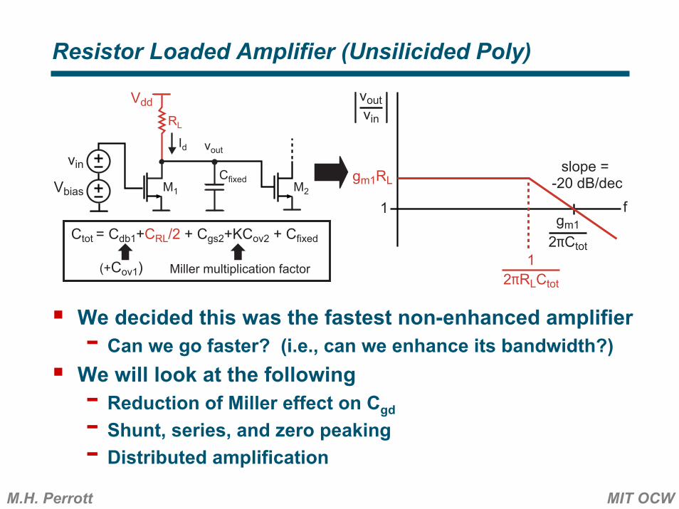
We decided this was the fastest non-enhanced amplifier- Can we go faster? (i.e., can we enhance its bandwidth?)
We will look at the following- Reduction of Miller effect on Cgd- Shunt, series, and zero peaking- Distributed amplification
M1
RL
vout
M2
Cfixed
Id
Vbias
vin
Ctot = Cdb1+CRL/2 + Cgs2+KCov2 + Cfixed
Miller multiplication factor(+Cov1)
1
voutvin
f
slope = -20 dB/dec
gm12πCtot
gm1RL
2πRLCtot
1
Vdd
M.H. Perrott MIT OCW
Cgd is quite significant compared to Cgs- In 0.18µ CMOS, Cgd is about 45% the value of Cgs
Input capacitance calculation
- For 0.18µ CMOS, gain of 3, input cap is almost tripled over Cgs!
M1
RL
vout
CL
Id
Vbias
vin
CgdZin
Rs
Cgs
Miller Effect on Cgd Is Significant
M.H. Perrott MIT OCW
Reduction of Cgd Impact Using a Cascode Device
The cascode device lowers the gain seen by Cgd of M1
- For 0.18m CMOS and gain of 3, impact of Cgd is reduced by 30%:
Issue: cascoding lowers achievable voltage swing
M1
RL vout
CL
Vbias
vin
CgdZin
Rs
Cgs
Vbias2M2
M.H. Perrott MIT OCW
Source-Coupled Amplifier
Remove impact of Miller effect by sending signal through source node rather than drain node- Cgd not Miller multiplied AND impact of Cgs cut in half!
The bad news- Signal has to go through source node (Csb significant)- Power consumption doubled
M1
Vbias
vin
Cgd
Rs
M2
RL
Cgd
2Ibias
voutZin
M.H. Perrott MIT OCW
Neutralization
Consider canceling the effect of Cgd- Choose CN = Cgd- Charging of Cgd now provided by CN
Benefit: Impact of Cgd removedIssues:- How do we create the inverting amplifier?- What happens if CN is not precisely matched to Cgd?
M1
RL
vout
CL
Id
Vbias
vin
CgdZin
Rs
Cgs
-1CN
M.H. Perrott MIT OCW
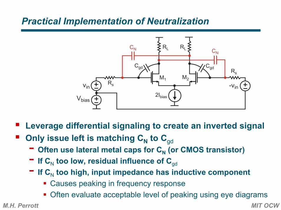
Practical Implementation of Neutralization
Leverage differential signaling to create an inverted signalOnly issue left is matching CN to Cgd- Often use lateral metal caps for CN (or CMOS transistor)- If CN too low, residual influence of Cgd- If CN too high, input impedance has inductive component
Causes peaking in frequency responseOften evaluate acceptable level of peaking using eye diagrams
M1
RL
Vbias
vin
Cgd
Rs
CN
M2
RL
Cgd
2Ibias
CN
-vin
Rs
M.H. Perrott MIT OCW
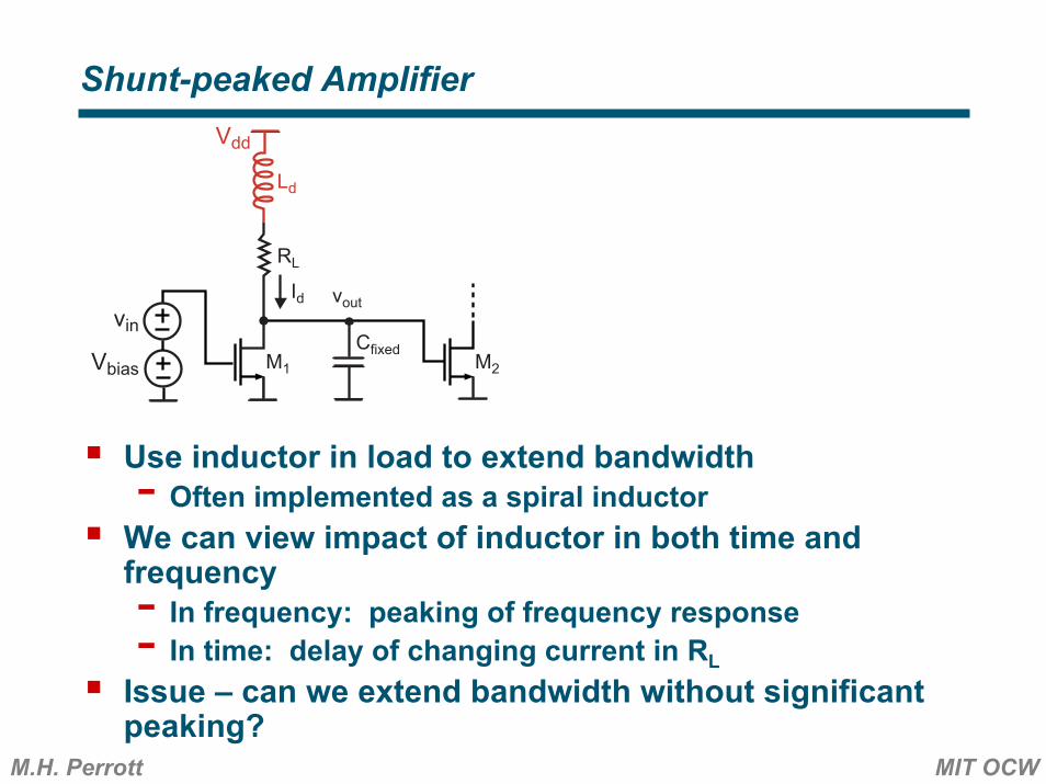
Shunt-peaked Amplifier
Use inductor in load to extend bandwidth- Often implemented as a spiral inductorWe can view impact of inductor in both time and frequency- In frequency: peaking of frequency response- In time: delay of changing current in RL
Issue – can we extend bandwidth without significant peaking?
M1
RL
vout
M2
Cfixed
Id
Vbias
vin
Vdd
Ld
M.H. Perrott MIT OCW
Shunt-peaked Amplifier - Analysis
Expression for gain
Parameterize with
- Corresponds to ratio of RC to LR time constants
M1
RL
vout
M2
Cfixed
Id
Vbias
vin
Vdd
Ld
RL
Ld
Ctotiin=gmvin
vout
Small Signal ModelZout
M.H. Perrott MIT OCW
The Impact of Choosing Different Values of m – Part 1
Parameterized gain expression
Comparison of new and old 3 dB frequencies
Want to solve for w2/w1
RL
Ld
Ctotiin=gmvin
vout
Small Signal ModelZout
M.H. Perrott MIT OCW
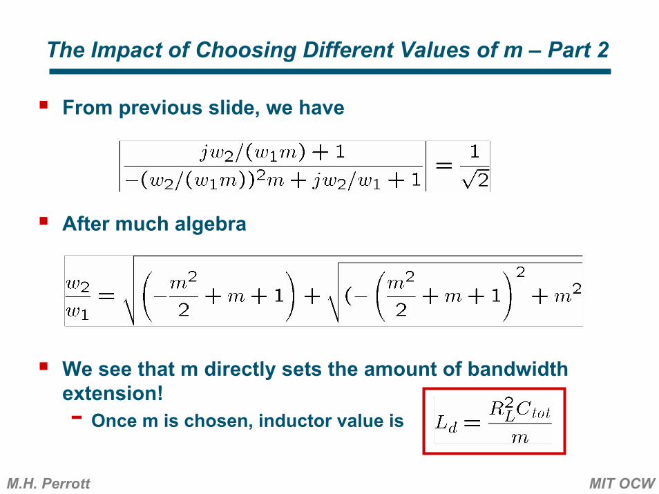
The Impact of Choosing Different Values of m – Part 2
From previous slide, we have
After much algebra
We see that m directly sets the amount of bandwidth extension!- Once m is chosen, inductor value is
M.H. Perrott MIT OCW
Plot of Bandwidth Extension Versus m
0 1 2 3 4 5 6 7 8 9 101.1
1.2
1.3
1.4
1.5
1.6
1.7
1.8
1.9
Bandwidth Extension (w2/w
1) Versus m
w1/w
2
m
Highest extension: w2/w1 = 1.85 at m ≈ 1.41- However, peaking occurs!
M.H. Perrott MIT OCW
Plot of Transfer Function Versus m
Maximum bandwidth: m = 1.41 (extension = 1.85)Maximally flat response: m = 2.41 (extension = 1.72)Best phase response: m = 3.1 (extension = 1.6)No peaking: m = infinityEye diagrams often used to evaluate best m
1/100 1/10 1 10 100-45
-40
-35
-30
-25
-20
-15
-10
-5
0
5
Nor
mal
ized
Gai
n (d
B)
Normalized Frequency (Hz)
Normalized Gain for Shunt Peaked Amplifier For Different m Values
m=1.41m=2.41
m=3.1m=infinity
M.H. Perrott MIT OCW
To Do
Add eye diagrams
M.H. Perrott MIT OCW
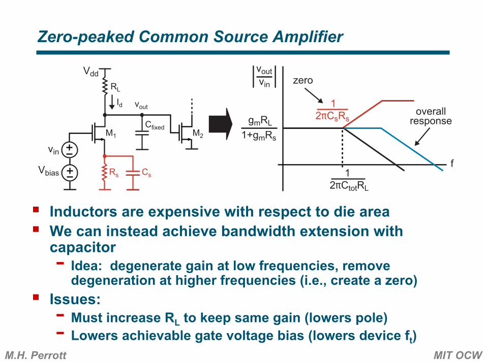
Zero-peaked Common Source Amplifier
Inductors are expensive with respect to die areaWe can instead achieve bandwidth extension with capacitor- Idea: degenerate gain at low frequencies, remove
degeneration at higher frequencies (i.e., create a zero)Issues:- Must increase RL to keep same gain (lowers pole)- Lowers achievable gate voltage bias (lowers device ft)
M1
RL
vout
M2
Cfixed
Id
Vbias
vin
Vdd
Rs Cs
voutvin
f
gmRL
2πCtotRL
1
2πCsRs
1
1+gmRs
zero
overallresponse
M.H. Perrott MIT OCW
Back to Inductors – Shunt and Series Peaking
Combine shunt peaking with a series inductor- Bandwidth extension by converting to a second order
filter responseCan be designed for proper peaking
Increases delay of amplifier
M1
RL
vout
M2
Cfixed
Id
Vbias
vin
Vdd
L1
L2
voutvin
f
gmRL
2πCtotRL
1
-40 dB/dec-20 dB/dec
M.H. Perrott MIT OCW
T-Coil Bandwidth Enhancement
Uses coupled inductors to realize T inductor network- Works best if capacitance at drain of M1 is much less than
the capacitance being driven at the output loadSee Chap. 8 of Tom Lee’s book (pp 187-191) for analysisSee S. Galal, B. Ravazi, “10 Gb/s Limiting Amplifier and Laser/Modulator Driver in 0.18u CMOS”, ISSCC 2003, pp 188-189 and “Broadband ESD Protection …”, pp. 182-183
M1
RL
vout
M2
Cfixed
Id
Vbias
vin
Vdd
L1
L2L3
M1
vout
M2
CfixedVbias
vin
L2
L1
CB
k
RL
Vdd
M.H. Perrott MIT OCW
Bandwidth Enhancement With ft Doublers
A MOS transistor has ft calculated as
ft doubler amplifiers attempt to increase the ratio of transconductance to capacitance
M1 M2
2Ibias
I1 I2
Vbias
vin
We can make the argument that differential amplifiers are ft doublers- Capacitance seen by Vin for single-ended input:- Difference in current:
Transconductance to Cap ratio is doubled:
M.H. Perrott MIT OCW
Creating a Single-Ended Output
Input voltage is again dropped across two transistors- Ratio given by voltage divider in capacitance
Ideally is ½ of input voltage on Cgs of each deviceInput voltage source sees the series combination of the capacitances of each device- Ideally sees ½ of the Cgs of M1
Currents of each device add to ideally yield ratio:
M1 M2
2Ibias
I1 I2
Vbias
vinM1
M2
Ibias
Io
Vbias
vin
Ibias
M.H. Perrott MIT OCW
Creating the Bias for M2
Use current mirror for bias- Inspired by bipolar circuits (see Tom Lee’s book, page 198)
Need to set Vbias such that current through M1 has the desired current of Ibias- The current through M2 will ideally match that of M1
Problem: achievable bias voltage across M1 (and M2) is severely reduced (thereby reducing effective ft of device)- Do ft doublers have an advantage in CMOS?
M1 M2
2Ibias
I1 I2
Vbias
vinM1
M2
Ibias
Io
Vbias
vin
Ibias
M1
M2
Io
Vbias
vin
IbiasM3
M.H. Perrott MIT OCW
Increasing Gain-Bandwidth Product Through Cascading
We can significantly increase the gain of an amplifier by cascading n stages
- Issue – bandwidth degrades, but by how much?
Amp Amp
Cfixed
Amp
Cfixed
A1 + s/wo
A1 + s/wo
A1 + s/wo
vin vout
vin vout
M.H. Perrott MIT OCW
Analytical Derivation of Overall Bandwidth
The overall 3-db bandwidth of the amplifier is where
- w1 is the overall bandwidth- A and wo are the gain and bandwidth of each section
- Bandwidth decreases much slower than gain increases!Overall gain bandwidth product of amp can be increased!
M.H. Perrott MIT OCW
Transfer Function for Cascaded Sections
1/100 1/10 1 10 100-80
-70
-60
-50
-40
-30
-20
-10
0
Nor
mal
ized
Gai
n (d
B)
Normalized Frequency (Hz)
Normalized Transfer Function for Cascaded Sections
n=1
n=2
n=3
n=4
-3
M.H. Perrott MIT OCW
Choosing the Optimal Number of Stages
To first order, there is a constant gain-bandwidth product for each stage
- Increasing the bandwidth of each stage requires that we lower its gain
- Can make up for lost gain by cascading more stagesWe found that the overall bandwidth is calculated as
Assume that we want to achieve gain G with n stages
From this, Tom Lee finds optimum gain ≈ 1.65- See Tom Lee’s book, pp 207-211
M.H. Perrott MIT OCW
Achievable Bandwidth Versus G and n
0 5 10 15 20 25 300
0.05
0.1
0.15
0.2
0.25
Achievable Bandwidth (Normalized to f )t Versus Gain (G) and Number of Stages (n)
n
w1/
wt
0.3
A=1.65
A=3
G=10
G=100
G=1000
Optimum gain per stage is about 1.65- Note than gain
per stage derived from plot as
- Maximum is fairly soft, though
Can dramatically lower power (and improve noise) by using larger gain per stage
M.H. Perrott MIT OCW
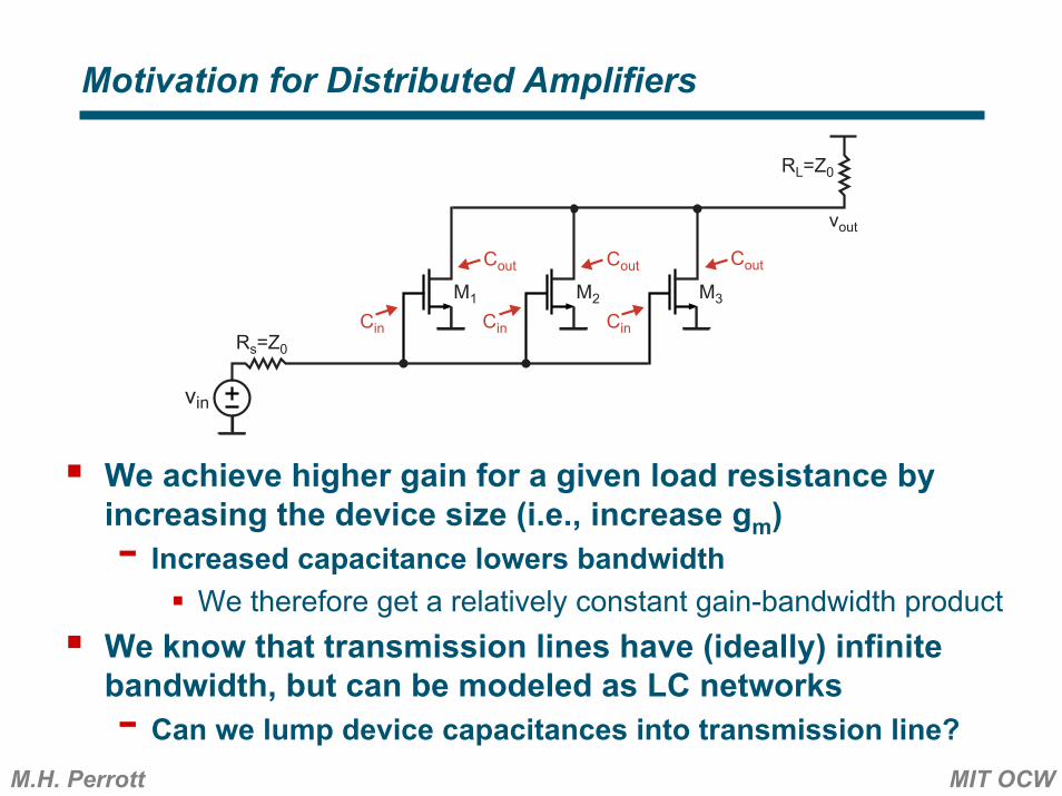
Motivation for Distributed Amplifiers
We achieve higher gain for a given load resistance by increasing the device size (i.e., increase gm)- Increased capacitance lowers bandwidth
We therefore get a relatively constant gain-bandwidth productWe know that transmission lines have (ideally) infinite bandwidth, but can be modeled as LC networks- Can we lump device capacitances into transmission line?
M1 M2 M3
vout
vin
Rs=Z0
RL=Z0
Cin CinCin
Cout Cout Cout
M.H. Perrott MIT OCW
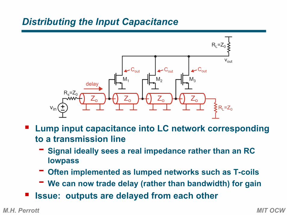
Distributing the Input Capacitance
Lump input capacitance into LC network corresponding to a transmission line- Signal ideally sees a real impedance rather than an RC
lowpass- Often implemented as lumped networks such as T-coils- We can now trade delay (rather than bandwidth) for gain
Issue: outputs are delayed from each other
M1 M2 M3
Zo Zo Zo Zo
vout
RL=Z0
delay
vin
Rs=Z0
RL=Z0
Cout Cout Cout
M.H. Perrott MIT OCW
Distributing the Output Capacitance
Delay the outputs same amount as the inputs- Now the signals match up- We have also distributed the output capacitance!
Benefit – high bandwidthNegatives – high power, poorer noise performance, expensive in terms of chip area- Each transistor gain is adding rather than multiplying!
M1
Zo Zo Zo Zo
M2 M3
Zo Zo Zo Zo
RL=Z0
vout
RL=Z0
delay
delay
vin
Rs=Z0
RL=Z0
M.H. Perrott MIT OCW
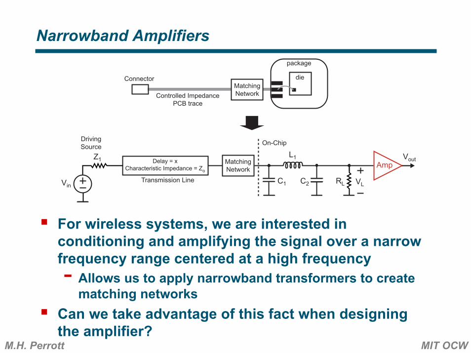
Narrowband Amplifiers
For wireless systems, we are interested in conditioning and amplifying the signal over a narrow frequency range centered at a high frequency- Allows us to apply narrowband transformers to create
matching networksCan we take advantage of this fact when designing the amplifier?
VLC1 RL
L1Delay = xCharacteristic Impedance = Zo
Transmission Line
Z1
VinC2
dieConnector
Controlled ImpedancePCB trace
package
On-ChipDrivingSource
AmpVout
MatchingNetwork
MatchingNetwork
M.H. Perrott MIT OCW
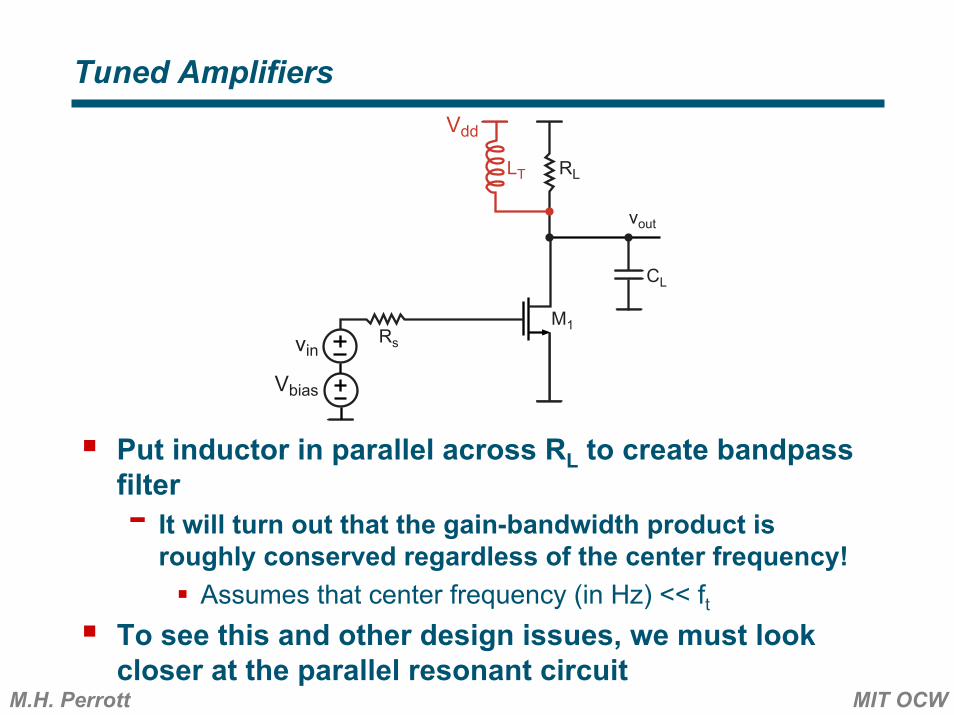
Tuned Amplifiers
Put inductor in parallel across RL to create bandpassfilter- It will turn out that the gain-bandwidth product is
roughly conserved regardless of the center frequency!Assumes that center frequency (in Hz) << ft
To see this and other design issues, we must look closer at the parallel resonant circuit
M1
vout
CL
Vbias
vinRs
Vdd
LT RL
M.H. Perrott MIT OCW
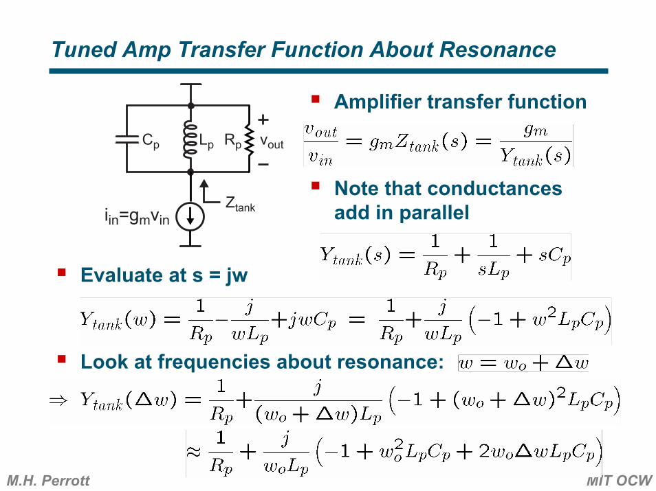
Tuned Amp Transfer Function About Resonance
Evaluate at s = jw
Look at frequencies about resonance:
RpLpCp
iin=gmvinZtank
vout
Amplifier transfer function
Note that conductancesadd in parallel
M.H. Perrott MIT OCW
Tuned Amp Transfer Function About Resonance (Cont.)
From previous slide
Simplifies to RC circuit for bandwidth calculation!
=0
RpLpCp
iin=gmvinZtank
vout
voutvin
w
slope =-20 dB/dec
gmRp
Rp2Cp
1
wo
Rp2Cp
1
RpCp
1
M.H. Perrott MIT OCW
Gain-Bandwidth Product for Tuned Amplifiers
The gain-bandwidth product:
The above expression is independent of center frequency!- In practice, we need to operate at a frequency less than
the ft of the device
RpLpCp
iin=gmvinZtank
vout
voutvin
w
slope =-20 dB/dec
gmRp
Rp2Cp
1
wo
Rp2Cp
1
RpCp
1
M.H. Perrott MIT OCW
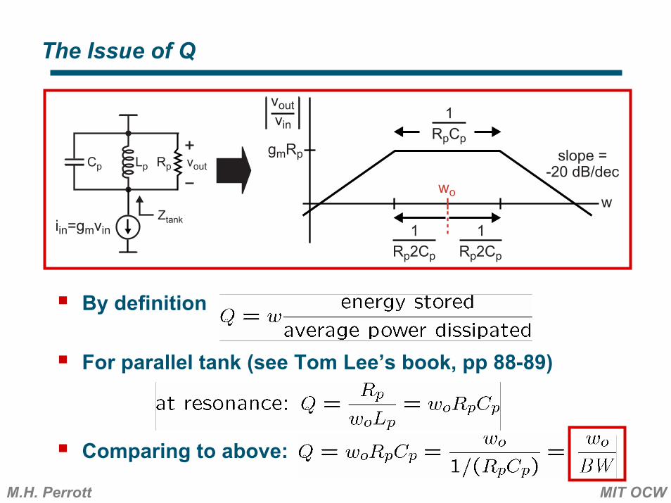
By definition
For parallel tank (see Tom Lee’s book, pp 88-89)
Comparing to above:
The Issue of Q
RpLpCp
iin=gmvinZtank
vout
voutvin
w
slope =-20 dB/dec
gmRp
Rp2Cp
1
wo
Rp2Cp
1
RpCp
1
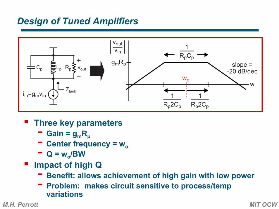
M.H. Perrott MIT OCW
Three key parameters- Gain = gmRp- Center frequency = wo- Q = wo/BWImpact of high Q - Benefit: allows achievement of high gain with low power- Problem: makes circuit sensitive to process/temp
variations
Design of Tuned Amplifiers
RpLpCp
iin=gmvinZtank
vout
voutvin
w
slope =-20 dB/dec
gmRp
Rp2Cp
1
wo
Rp2Cp
1
RpCp
1
M.H. Perrott MIT OCW
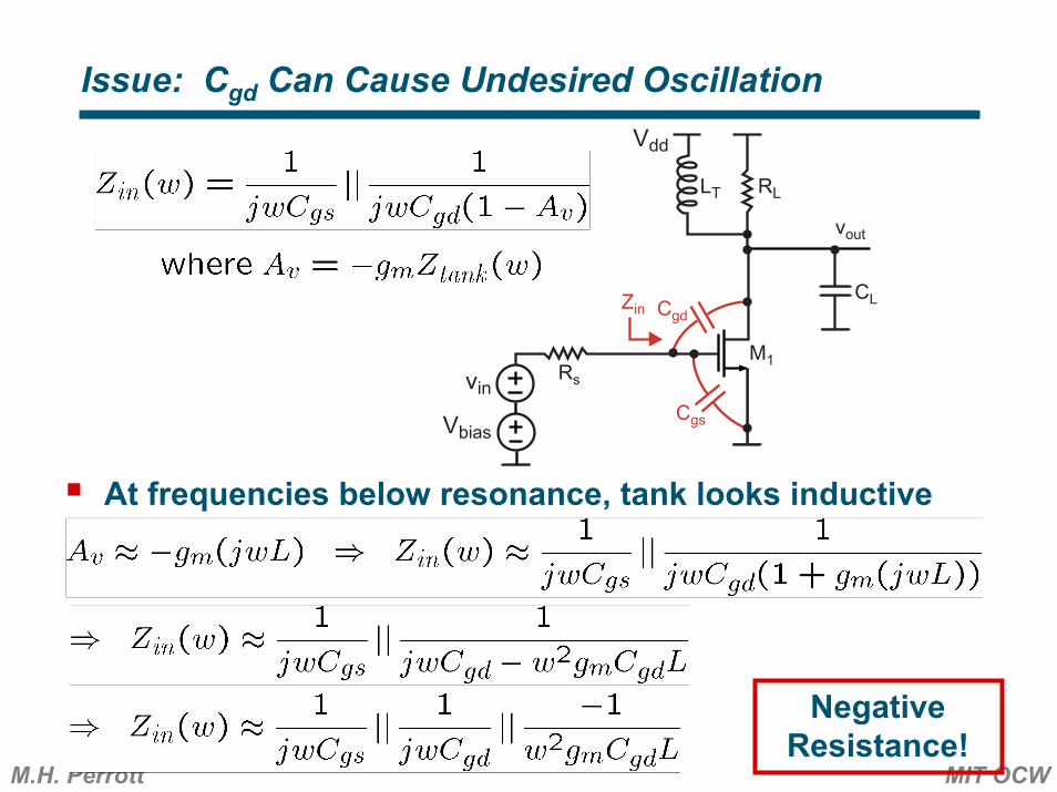
Issue: Cgd Can Cause Undesired Oscillation
At frequencies below resonance, tank looks inductive
M1
vout
CL
Vbias
vin
CgdZin
Rs
Cgs
Vdd
LT RL
NegativeResistance!
M.H. Perrott MIT OCW
Use Cascode Device to Remove Impact of Cgd
At frequencies above and below resonance
M1
vout
CL
Vbias
vin
CgdZin
Rs
Cgs
Vbias2M2
Vdd
LT RL
PurelyCapacitive!
M.H. Perrott MIT OCW
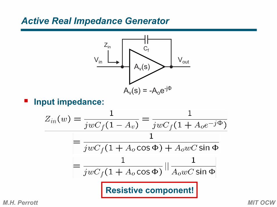
Active Real Impedance Generator
Input impedance:
Zin
Av(s)VoutVin
Av(s) = -Aoe-jΦ
Cf
Resistive component!
M.H. Perrott MIT OCW
This Principle Can Be Applied To Impedance Matching
We will see that it’s advantageous to make Zin real without using resistors- For the above circuit (ignoring Cgd)
M1
Vbias
vinRs
Ls
ZinIout
Ls
vgs gmvgsCgsItest Vtest
Looks like series resonant circuit!
M.H. Perrott MIT OCW
Use A Series Inductor to Tune Resonant Frequency
Calculate input impedance with added inductor
Often want purely resistive component at frequency wo- Choose Lg such that resonant frequency = wo