41
6.976 High Speed Communication Circuits and Systems Lecture 5 High Speed, Broadband Amplifiers Michael Perrott Massachusetts Institute of Technology Copyright © 2003 by Michael H. Perrott

6.976High Speed Communication Circuits and Systems
Lecture 5High Speed, Broadband Amplifiers
Michael PerrottMassachusetts Institute of Technology
Copyright © 2003 by Michael H. Perrott
M.H. Perrott MIT OCW
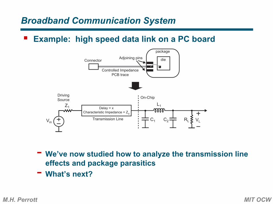
Broadband Communication System
Example: high speed data link on a PC board
- We’ve now studied how to analyze the transmission line effects and package parasitics
- What’s next?
VLC1 RL
L1Delay = xCharacteristic Impedance = Zo
Transmission Line
Z1
VinC2
dieAdjoining pinsConnector
Controlled ImpedancePCB trace
package
On-ChipDrivingSource
M.H. Perrott MIT OCW
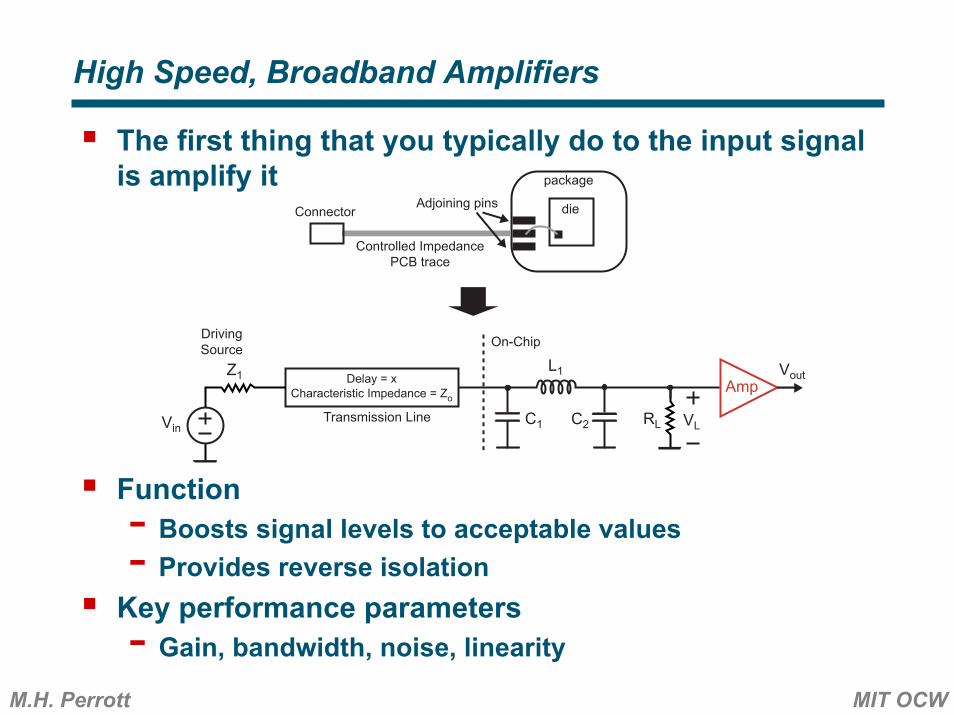
High Speed, Broadband Amplifiers
The first thing that you typically do to the input signal is amplify it
Function- Boosts signal levels to acceptable values- Provides reverse isolation
Key performance parameters- Gain, bandwidth, noise, linearity
VLC1 RL
L1Delay = xCharacteristic Impedance = Zo
Transmission Line
Z1
VinC2
dieAdjoining pinsConnector
Controlled ImpedancePCB trace
package
On-ChipDrivingSource
AmpVout

M.H. Perrott MIT OCW
Basics of MOS Large Signal Behavior (Qualitative)
S D
G
Cchannel = Cox(VGS-VT)
VGS
VDS=0
S D
GVGS
VD=∆V
S D
GVGS
VD>∆V
Triode
Pinch-off
SaturationVDS
ID
ID
ID
ID
Triode
Pinch-offSaturation
∆V
Overall I-V Characteristic
M.H. Perrott MIT OCW
Basics of MOS Large Signal Behavior (Quantitative)
S D
G
Cchannel = Cox(VGS-VT)
VGS
VDS=0
S D
GVGS
VD=∆V
S D
GVGS
VD>∆V
Triode
Pinch-off
Saturation
ID
ID
ID
ID = µnCoxWL
(VGS - VT - VDS/2)VDS
ID µnCoxWL
(VGS - VT)VDS
for VDS << VGS - VT
ID = µnCoxWL
12
(VGS-VT)2(1+λVDS)
(where λ corresponds tochannel length modulation)
∆V = VGS-VT
∆V =µnCoxW
2IDL
M.H. Perrott MIT OCW
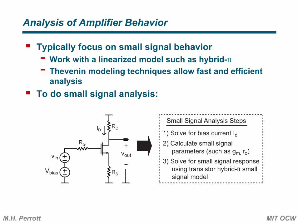
Analysis of Amplifier Behavior
Typically focus on small signal behavior- Work with a linearized model such as hybrid-π- Thevenin modeling techniques allow fast and efficient
analysisTo do small signal analysis:
RS
RG
RD
vinvout
Vbias
ID 1) Solve for bias current Id2) Calculate small signal parameters (such as gm, ro)3) Solve for small signal response using transistor hybrid-π small signal model
Small Signal Analysis Steps

M.H. Perrott MIT OCW
MOS DC Small Signal Model
Assume transistor in saturation:
Thevenin modeling based on the above
RS
RG
RDRD
RS
RG
-gmbvsvgs
vs
rogmvgs
gm = µnCox(W/L)(VGS - VT)(1 + λVDS)
= 2µnCox(W/L)ID (assuming λVDS << 1)
Cox
2qεsNA
2 2|Φp| + VSB
γgm where γ =gmb =
In practice: gmb = gm/5 to gm/3
λID1ro =
ID

M.H. Perrott MIT OCW
Capacitors For MOS Device In Saturation
S D
GVGS
VD>∆V
ID
LDLD
overlap cap: Cov = WLDCox + WCfringe
B
CgcCcb
Cov
CjdbCjsb
Cov
Side View
gate to channel cap: Cgc = CoxW(L-2LD)
channel to bulk cap: Ccb - ignore in this class
S D
Top View
W
E
L
E
E
source to bulk cap: Cjsb = 1 + VSB ΦB
Cj(0)
1 + VSB ΦB
Cjsw(0)WE + (W + 2E)
junction bottom wall cap (per area)
junction sidewall cap (per length)
drain to bulk cap: Cjsd = 1 + VDB ΦB
Cj(0)
1 + VDB ΦB
Cjsw(0)WE + (W + 2E)
23
(make 2W for "4 sided" perimeter in some cases)
L
M.H. Perrott MIT OCW
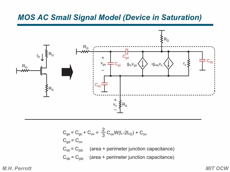
MOS AC Small Signal Model (Device in Saturation)
RS
RG
RD
RD
RS
RG
-gmbvsvgs
vs
rogmvgs
ID
Csb
Cgs
CgdCdb
Cgs = Cgc + Cov = CoxW(L-2LD) + Cov23
Cgd = Cov
Csb = Cjsb (area + perimeter junction capacitance)
Cdb = Cjdb (area + perimeter junction capacitance)

M.H. Perrott MIT OCW
Wiring Parasitics
Capacitance- Gate: cap from poly to substrate and metal layers- Drain and source: cap from metal routing path to
substrate and other metal layersResistance- Gate: poly gate has resistance (reduced by silicide)- Drain and source: some resistance in diffusion region,
and from routing long metal linesInductance- Gate: poly gate has negligible inductance- Drain and source: becoming an issue for long wires
Extract these parasitics from circuit layout
M.H. Perrott MIT OCW
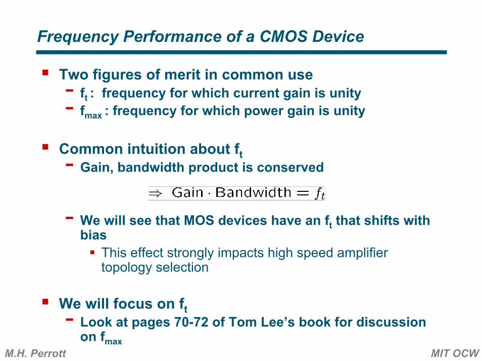
Frequency Performance of a CMOS Device
Two figures of merit in common use- ft : frequency for which current gain is unity- fmax : frequency for which power gain is unity
Common intuition about ft- Gain, bandwidth product is conserved
- We will see that MOS devices have an ft that shifts with bias
This effect strongly impacts high speed amplifier topology selection
We will focus on ft- Look at pages 70-72 of Tom Lee’s book for discussion on fmax

M.H. Perrott MIT OCW
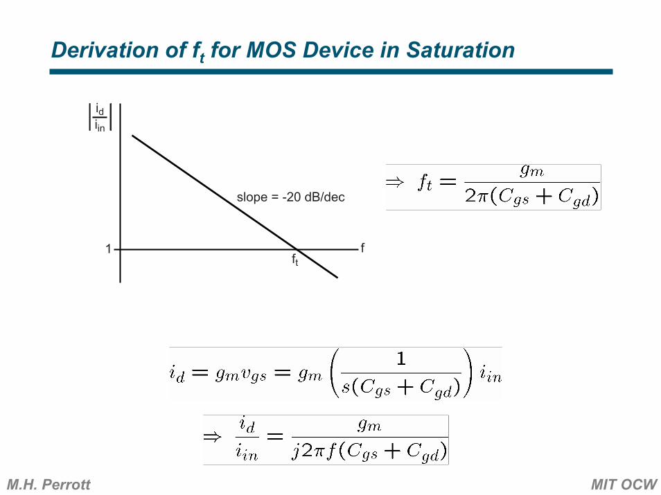
Derivation of ft for MOS Device in Saturation
Assumption is that input is current, output of device is short circuited to a supply voltage- Note that voltage bias is required at gate
The calculated value of ft is a function of this bias voltage
-gmbvsvgs rogmvgs
ID+id
Csb
Cgs
CgdCdb
iinVbias
RLARGE
id
iin

M.H. Perrott MIT OCW
Derivation of ft for MOS Device in Saturation
-gmbvsvgs rogmvgs
ID+id
Csb
Cgs
CgdCdb
iinVbias
RLARGE
id
iin
M.H. Perrott MIT OCW
Derivation of ft for MOS Device in Saturation
1
idiin
fft
slope = -20 dB/dec
M.H. Perrott MIT OCW
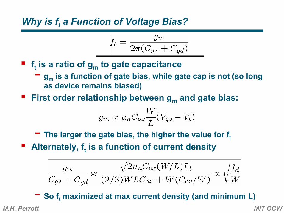
Why is ft a Function of Voltage Bias?
ft is a ratio of gm to gate capacitance- gm is a function of gate bias, while gate cap is not (so long
as device remains biased)First order relationship between gm and gate bias:
- The larger the gate bias, the higher the value for ft
Alternately, ft is a function of current density
- So ft maximized at max current density (and minimum L)
M.H. Perrott MIT OCW
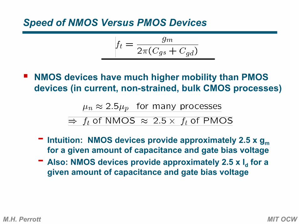
Speed of NMOS Versus PMOS Devices
NMOS devices have much higher mobility than PMOS devices (in current, non-strained, bulk CMOS processes)
- Intuition: NMOS devices provide approximately 2.5 x gmfor a given amount of capacitance and gate bias voltage
- Also: NMOS devices provide approximately 2.5 x Id for a given amount of capacitance and gate bias voltage

M.H. Perrott MIT OCW
Assumptions for High Speed Amplifier Analysis
Assume that amplifier is loaded by an identical amplifier and by fixed wiring capacitance
Intrinsic performance- Defined as the bandwidth achieved for a given gain when Cfixed is negligible- Amplifier approaches intrinsic performance as its device sizes (and current) are increased
In practice, optimal sizing (and power) of amplifier is roughly where Cin+Cout = Cfixed
Amp Amp
Cfixed
CinCin
Ctot = Cout+Cin+Cfixed
Cout
M.H. Perrott MIT OCW
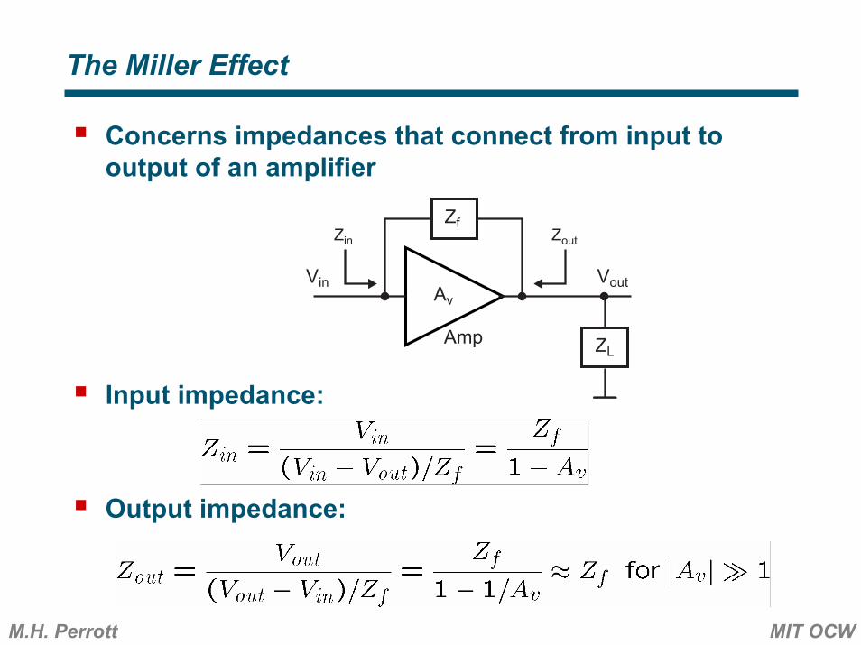
The Miller Effect
Concerns impedances that connect from input to output of an amplifier
Input impedance:
Output impedance:
Amp
Zin
Zf
Av
ZL
VoutVin
Zout
M.H. Perrott MIT OCW
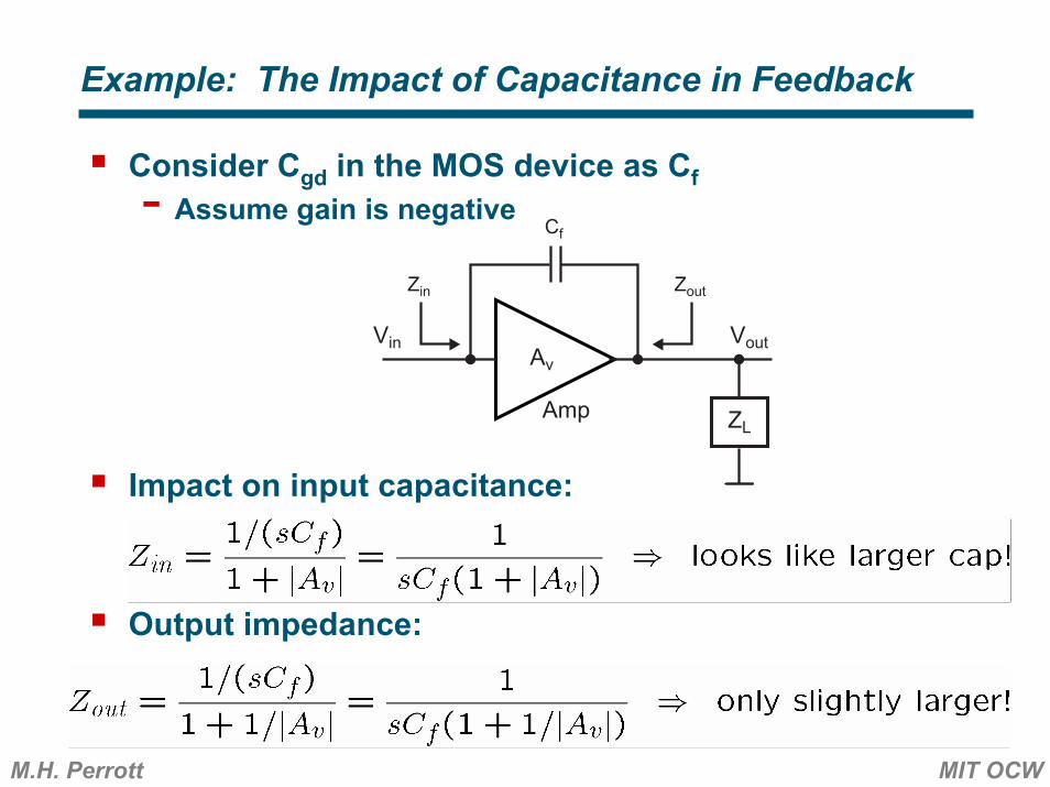
Example: The Impact of Capacitance in Feedback
Consider Cgd in the MOS device as Cf- Assume gain is negative
Impact on input capacitance:
Output impedance:
Amp
Zin
Av
ZL
VoutVin
Zout
Cf
M.H. Perrott MIT OCW
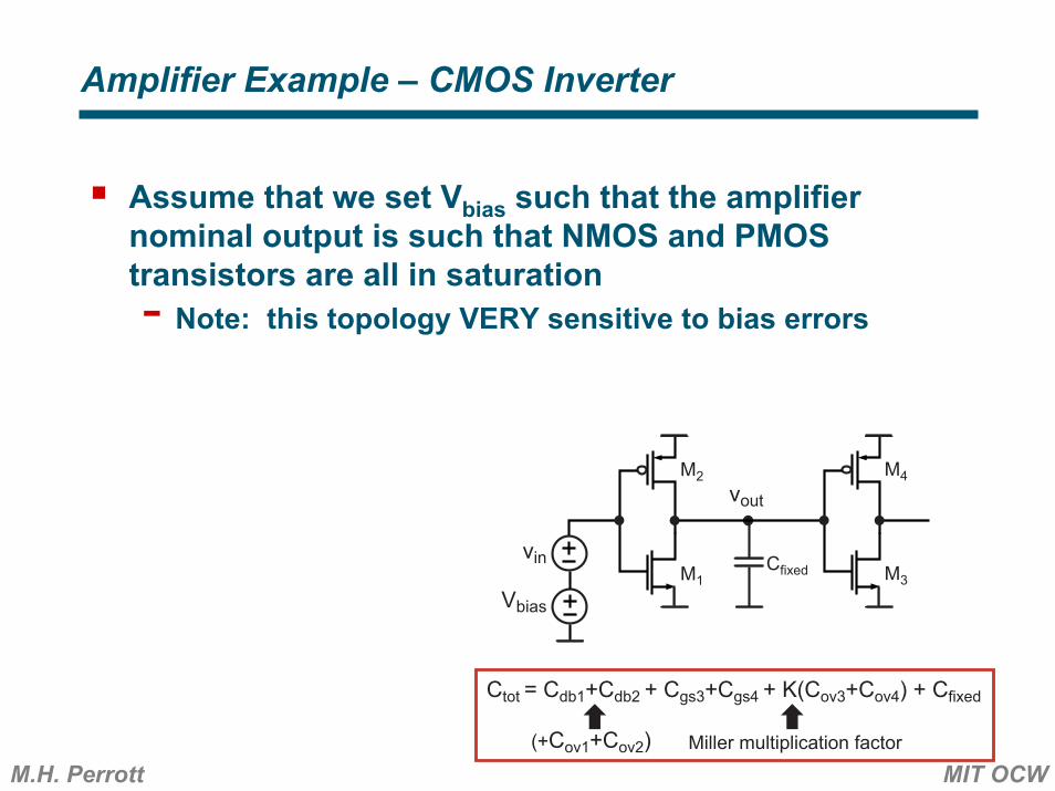
Amplifier Example – CMOS Inverter
Assume that we set Vbias such that the amplifier nominal output is such that NMOS and PMOS transistors are all in saturation- Note: this topology VERY sensitive to bias errors
Cfixed
Ctot = Cdb1+Cdb2 + Cgs3+Cgs4 + K(Cov3+Cov4) + Cfixed
M2
M1
M4
M3
Miller multiplication factor
Vbias
vin
(+Cov1+Cov2)
vout

M.H. Perrott MIT OCW
Transfer Function of CMOS Inverter
Low Bandwidth!
Cfixed
Ctot = Cdb1+Cdb2 + Cgs3+Cgs4 + K(Cov3+Cov4) + Cfixed
M2
M1
M4
M3
Miller multiplication factor
Vbias
vin
(+Cov1+Cov2)
vout
1
voutvin
f
slope = -20 dB/dec
(gm1+gm2)(ro1||ro2)
2πCtot(ro1||ro2)1 gm1+gm2
2πCtot

M.H. Perrott MIT OCW
Add Resistive Feedback
Bandwidth extended andless sensitivityto bias offset
Cfixed
Ctot = Cdb1+Cdb2 + Cgs3+Cgs4 + K(Cov3+Cov4) + CRf /2 + Cfixed
M2
M1
M4
M3
Miller multiplication factor
Vbias
vin
(+Cov1+Cov2)
voutRf
1
voutvin
f
slope = -20 dB/dec
(gm1+gm2)(ro1||ro2)
2πCtot(ro1||ro2)1 gm1+gm2
2πCtot
(gm1+gm2)Rf
2πCtotRf
1
M.H. Perrott MIT OCW
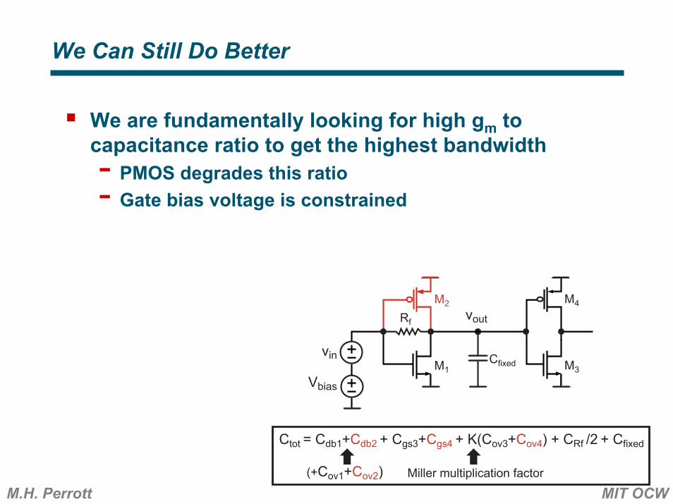
We Can Still Do Better
We are fundamentally looking for high gm to capacitance ratio to get the highest bandwidth- PMOS degrades this ratio- Gate bias voltage is constrained
Cfixed
Ctot = Cdb1+Cdb2 + Cgs3+Cgs4 + K(Cov3+Cov4) + CRf /2 + Cfixed
M2
M1
M4
M3
Miller multiplication factor
Vbias
vin
(+Cov1+Cov2)
voutRf
M.H. Perrott MIT OCW
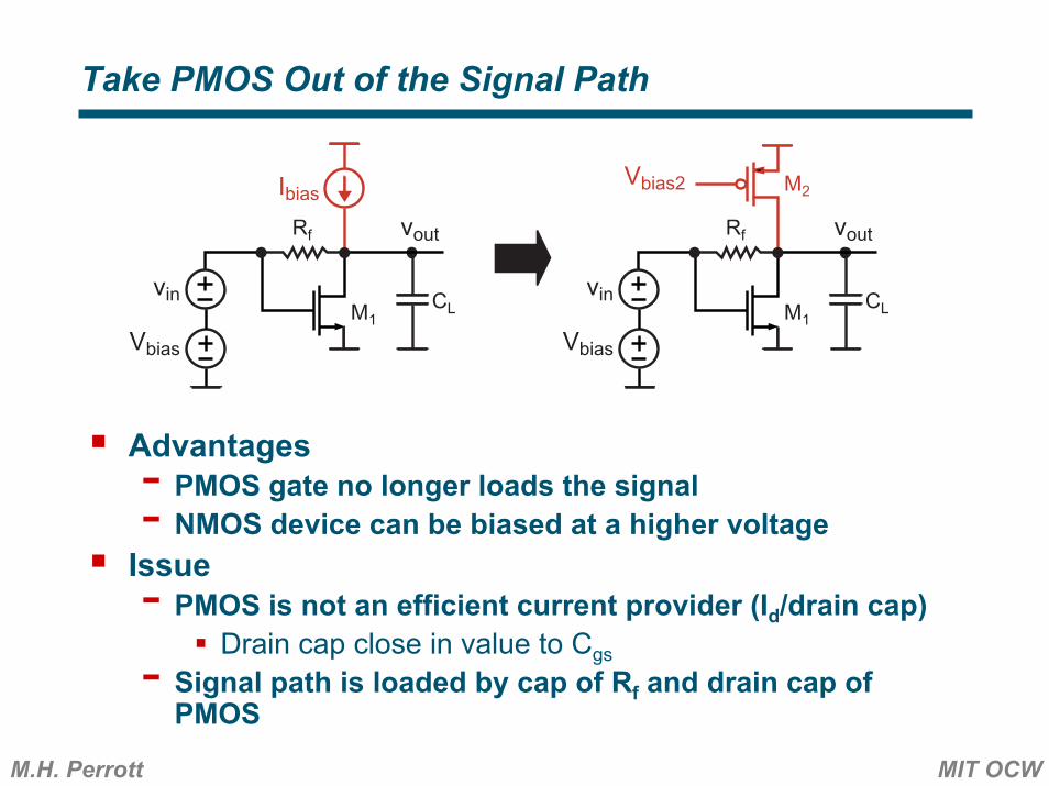
Take PMOS Out of the Signal Path
Advantages- PMOS gate no longer loads the signal- NMOS device can be biased at a higher voltageIssue- PMOS is not an efficient current provider (Id/drain cap)
Drain cap close in value to Cgs- Signal path is loaded by cap of Rf and drain cap of PMOS
CL
M2
M1Vbias
vin
voutRf
Vbias2Ibias
CLM1Vbias
vin
voutRf
M.H. Perrott MIT OCW
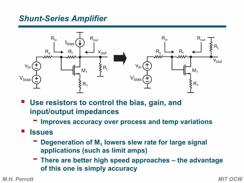
Shunt-Series Amplifier
Use resistors to control the bias, gain, and input/output impedances- Improves accuracy over process and temp variations
Issues- Degeneration of M1 lowers slew rate for large signal
applications (such as limit amps)- There are better high speed approaches – the advantage
of this one is simply accuracy
Ibias
M1
Vbias
vin
voutRf
R1
Rs
RL
Rin Rout
M1
Vbias
vinvout
Rf
R1
Rs
RL
Rin Rout
M.H. Perrott MIT OCW
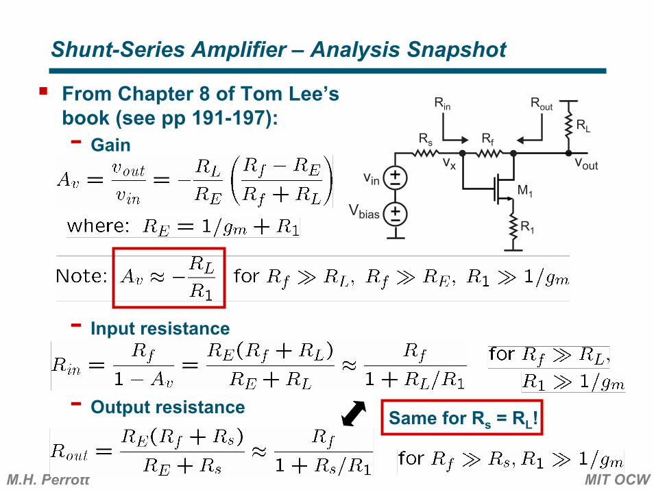
Shunt-Series Amplifier – Analysis Snapshot
From Chapter 8 of Tom Lee’s book (see pp 191-197):- Gain
- Input resistance
- Output resistance
M1
Vbias
vinvout
Rf
R1
Rs
RL
Rin Rout
vx
Same for Rs = RL!

M.H. Perrott MIT OCW
NMOS Load Amplifier
Gain set by the relative sizing of M1 and M2
CfixedM1Vbias
vin
vout
M2
gm2
1
1
voutvin
f
slope = -20 dB/dec
gm12πCtot
gm1
2πCtot
gm2
gm2Ctot = Cdb1+Csb2+Cgs2 + Cgs3+KCov3 + Cfixed
Miller multiplication factor(+Cov1)
M3
Vdd
Id
M.H. Perrott MIT OCW
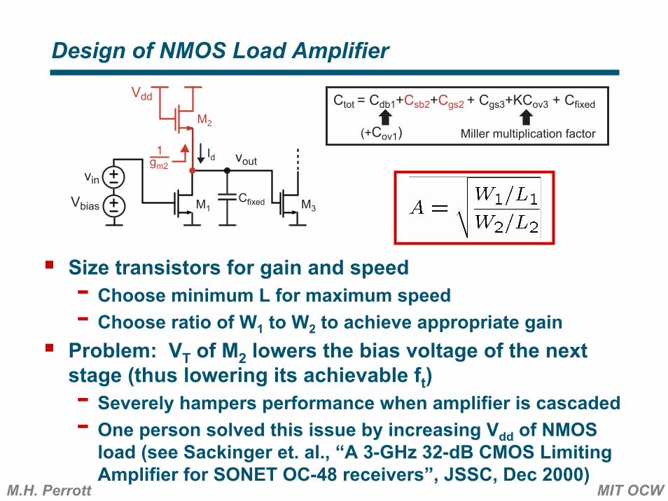
Design of NMOS Load Amplifier
Size transistors for gain and speed- Choose minimum L for maximum speed- Choose ratio of W1 to W2 to achieve appropriate gain
Problem: VT of M2 lowers the bias voltage of the next stage (thus lowering its achievable ft)- Severely hampers performance when amplifier is cascaded- One person solved this issue by increasing Vdd of NMOS
load (see Sackinger et. al., “A 3-GHz 32-dB CMOS Limiting Amplifier for SONET OC-48 receivers”, JSSC, Dec 2000)
CfixedM1Vbias
vin
vout
M2
gm2
1
Ctot = Cdb1+Csb2+Cgs2 + Cgs3+KCov3 + Cfixed
Miller multiplication factor(+Cov1)
M3
Vdd
Id

M.H. Perrott MIT OCW
Resistor Loaded Amplifier (Unsilicided Poly)
This is the fastest non-enhanced amplifier I’ve found- Unsilicided poly is a pretty efficient current provider
(i..e, has a good current to capacitance ratio)- Output swing can go all the way up to Vdd
Allows following stage to achieve high ft- Linear settling behavior (in contrast to NMOS load)
M1
RL
vout
M2
Cfixed
Id
Vbias
vin
Ctot = Cdb1+CRL/2 + Cgs2+KCov2 + Cfixed
Miller multiplication factor(+Cov1)
1
voutvin
f
slope = -20 dB/dec
gm12πCtot
gm1RL
2πRLCtot
1
Vdd
M.H. Perrott MIT OCW
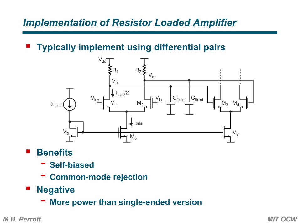
Implementation of Resistor Loaded Amplifier
Typically implement using differential pairs
Benefits- Self-biased- Common-mode rejection
Negative- More power than single-ended version
M6
M1 M2
M5
αIbias
Vin+
R1
Vin-
R2Vo+
Vo-
M7
M3 M4
Cfixed Cfixed
Ibias
Ibias/2
Vdd

M.H. Perrott MIT OCW
The Issue of Velocity Saturation
We classically assume that MOS current is calculated as
Which is really
- Vdsat,l corresponds to the saturation voltage at a given length, which we often refer to as ∆V
It may be shown that
- If Vgs-VT approaches LEsat in value, then the top equation is no longer valid
We say that the device is in velocity saturation

M.H. Perrott MIT OCW
Analytical Device Modeling in Velocity Saturation
If L small (as in modern devices), than velocity saturation will impact us for even moderate values of Vgs-VT
- Current increases linearly with Vgs-VT!Transconductance in velocity saturation:
- No longer a function of Vgs!
M.H. Perrott MIT OCW
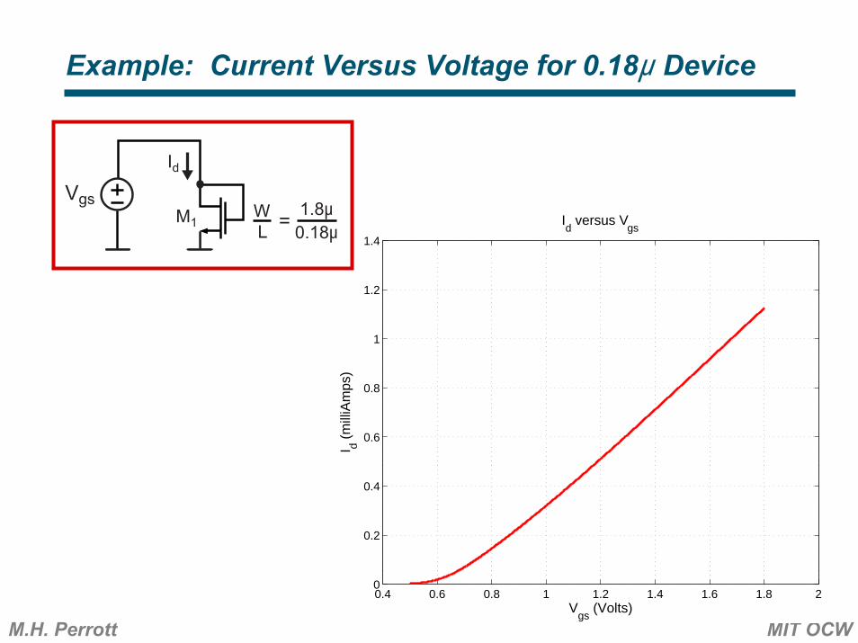
Example: Current Versus Voltage for 0.18µ Device
0.4 0.6 0.8 1 1.2 1.4 1.6 1.8 20
0.2
0.4
0.6
0.8
1
1.2
1.4
Vgs
(Volts)
I d (m
illiA
mps
)
Id versus V
gsM1
IdVgs
WL = 1.8µ
0.18µ
M.H. Perrott MIT OCW
0.4 0.6 0.8 1 1.2 1.4 1.6 1.8 20
0.1
0.2
0.3
0.4
0.5
0.6
0.7
0.8
0.9
1
Vgs
(Volts)
g m (
mill
iAm
ps/V
olts
)
gm
versus Vgs
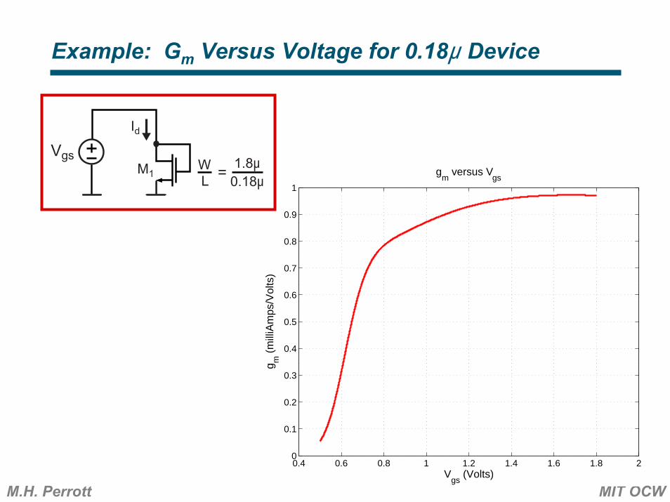
Example: Gm Versus Voltage for 0.18µ Device
M1
IdVgs
WL = 1.8µ
0.18µ

M.H. Perrott MIT OCW0 100 200 300 400 500 600 700
0
0.2
0.4
0.6
0.8
1
Current Density (microAmps/micron)
Tra
nsco
nduc
tanc
e (m
illiA
mps
/Vol
ts)
Transconductance versus Current Density
Example: Gm Versus Current Density for 0.18µ Device
M1
IdVgs
WL = 1.8µ
0.18µ
M.H. Perrott MIT OCW
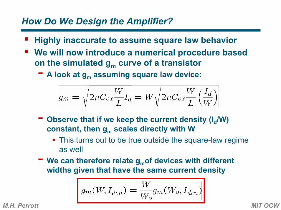
How Do We Design the Amplifier?
Highly inaccurate to assume square law behaviorWe will now introduce a numerical procedure based on the simulated gm curve of a transistor- A look at gm assuming square law device:
- Observe that if we keep the current density (Id/W) constant, then gm scales directly with W
This turns out to be true outside the square-law regime as well
- We can therefore relate gmof devices with different widths given that have the same current density
M.H. Perrott MIT OCW
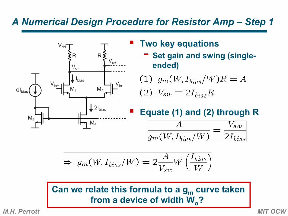
A Numerical Design Procedure for Resistor Amp – Step 1
Two key equations- Set gain and swing (single-
ended)
Equate (1) and (2) through RM6
M1 M2
M5
αIbias
Vin+
R
Vin-
RVo+
Vo-
2Ibias
Ibias
Vdd
Can we relate this formula to a gm curve takenfrom a device of width Wo?

M.H. Perrott MIT OCW
We now know:
Substitute (2) into (1)
The above expression allows us to design the resistor loaded amp based on the gm curve of a representative transistor of width Wo!
A Numerical Design Procedure for Resistor Amp – Step 2

M.H. Perrott MIT OCW
Example: Design for Swing of 1 V, Gain of 1 and 2
Assume L=0.18µ, use previous gm plot (Wo=1.8µ)
0 100 200 300 400 500 600 7000
0.2
0.4
0.6
0.8
1
Current Density - Iden (microAmps/micron)
Tran
scon
duct
ance
(m
illiA
mps
/Vol
ts)
Transconductance versus Current Density
A=2 A=1
gm(wo=1.8µ,Iden)
For gain of 1, current density = 250 µA/µmFor gain of 2, current density = 115 µA/µm Note that current density reduced as gain increases!- ft effectively
decreased

M.H. Perrott MIT OCW
Example (Continued)
Knowledge of the current density allows us to design the amplifier- Recall- Free parameters are W, Ibias, and R (L assumed to be fixed)
Given Iden = 115 µA/µm (Swing = 1V, Gain = 2)- If we choose Ibias = 300 µA
Note that we could instead choose W or R, and then calculate the other parameters
M.H. Perrott MIT OCW
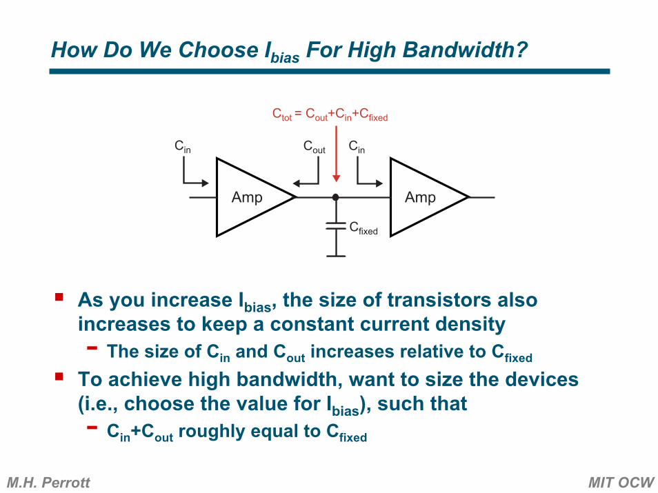
How Do We Choose Ibias For High Bandwidth?
As you increase Ibias, the size of transistors also increases to keep a constant current density- The size of Cin and Cout increases relative to Cfixed
To achieve high bandwidth, want to size the devices (i.e., choose the value for Ibias), such that - Cin+Cout roughly equal to Cfixed
Amp Amp
Cfixed
CinCin
Ctot = Cout+Cin+Cfixed
Cout


![Paulo MoreiraTechnology1 Outline Introduction – “Is there a limit ?” Transistors – “CMOS building blocks” Parasitics I – “The [un]desirables” Parasitics.](https://static.documents.pub/doc/80x56/56649d7e5503460f94a61dea/paulo-moreiratechnology1-outline-introduction-is-there-a-limit-.jpg)


