38
1 EE362L, Spring 2009 DCíDC Buck Converter
| Date post: | 08-Apr-2018 |
| Category: |
Documents |
| Upload: | kartheekvankadara |
| View: | 217 times |
| Download: | 0 times |

8/7/2019 _6_EE362L_DC_DC_Buck_PPT_Spring2009
http://slidepdf.com/reader/full/6ee362ldcdcbuckpptspring2009 1/38
1
EE362L, Spring 2009DCíDC Buck Converter

8/7/2019 _6_EE362L_DC_DC_Buck_PPT_Spring2009
http://slidepdf.com/reader/full/6ee362ldcdcbuckpptspring2009 2/38
2
!
N ote - Helper
From now on this symbol will identify slides in which there is avery important concept that needs to be clearly understood
However, a lack of the symbol in one slide does not imply thatthere is no important material or concept in the slides or thatthe slide does not need to be studied. Slides without thesymbol still need to be studied and could be necessary tosolve problems in exams.
8/7/2019 _6_EE362L_DC_DC_Buck_PPT_Spring2009
http://slidepdf.com/reader/full/6ee362ldcdcbuckpptspring2009 3/38
3
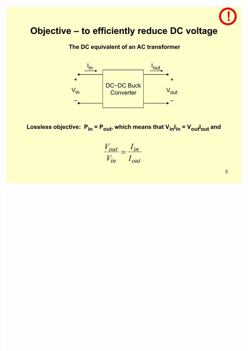
Objective ± to efficiently reduce DC voltage
DCíDC BuckConverter
+
Vin
í
+
Vout
í
IoutIin
Lossless objective: P in = P out , which means that V in Iin = Vout Iout and
The DC equivalent of an AC transformer
out
in
in
out
I I
V V !
!
8/7/2019 _6_EE362L_DC_DC_Buck_PPT_Spring2009
http://slidepdf.com/reader/full/6ee362ldcdcbuckpptspring2009 4/38
4
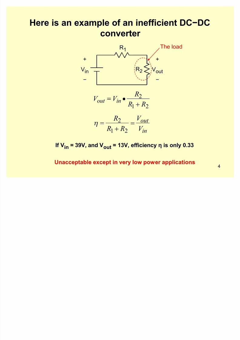
Here is an example of an inefficient DCíDCconverter
21
2
RR
RV V inout y
+
Vin
í
+
Vout
í
R1
R2
in
out V
V
RR
R
!! 21
2
L
If Vin = 39V, and V out = 13V, efficiency is only 0.33
Th e load
Unacceptable except in very low power applications

8/7/2019 _6_EE362L_DC_DC_Buck_PPT_Spring2009
http://slidepdf.com/reader/full/6ee362ldcdcbuckpptspring2009 5/38
5
Another method ± lossless conversion of 39Vdc to average 13Vdc
If the duty cycle D of the switch is 0.33, then the averagevoltage to the expensive car stereo is 39 0.33 = 13Vdc. Thisis lossless conversion, but is it acceptable?
R stereo+
39Vdc±
Switch state, Stereo voltage
Closed, 39Vdc
Open, 0Vdc
Switch openStereovoltage
39
0
Switch closed
DT
T
Taken from ³Course Overview´ PPT !
8/7/2019 _6_EE362L_DC_DC_Buck_PPT_Spring2009
http://slidepdf.com/reader/full/6ee362ldcdcbuckpptspring2009 6/38
6
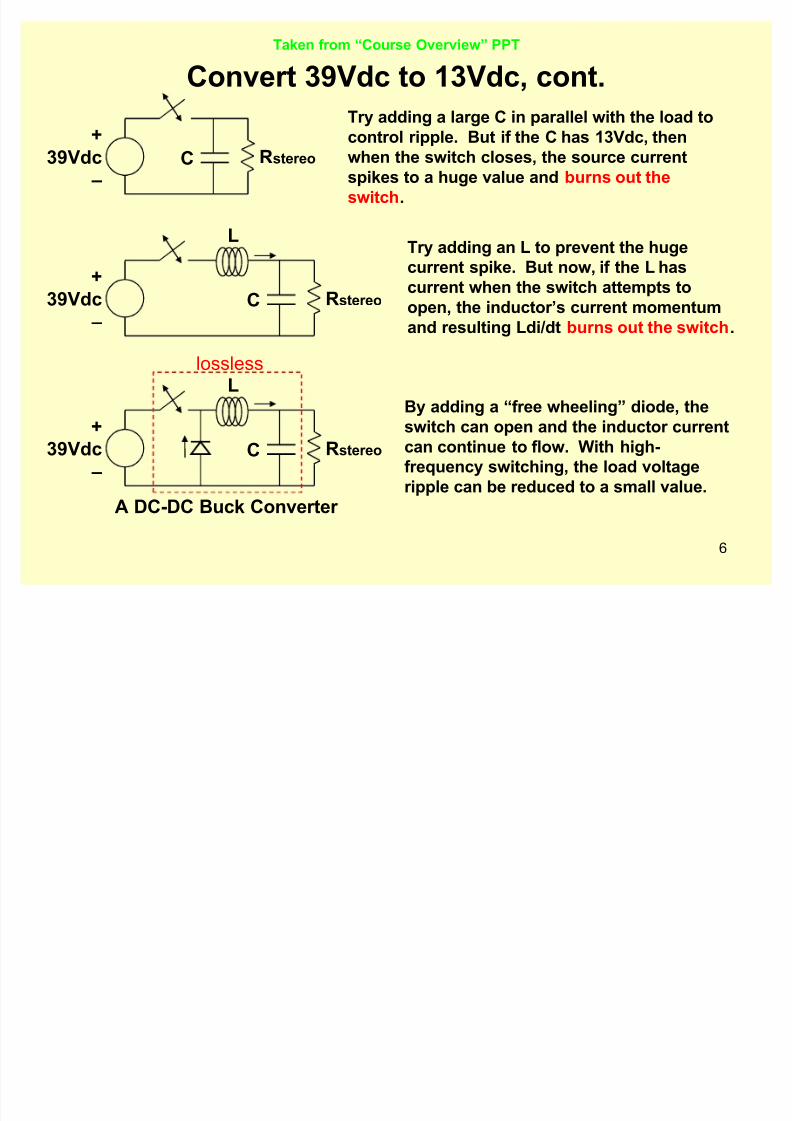
Convert 39Vdc to 13Vdc, cont.Try adding a large C in parallel with the load to
control ripple. But if the C has 13Vdc, thenwhen the switch closes, the source currentspikes to a huge value and burns out theswitch .
R stereo+
39Vdc±
C
Try adding an L to prevent the hugecurrent spike. But now, if the L hascurrent when the switch attempts toopen, the inductor¶s current momentumand resulting Ldi/dt burns out the switch .
By adding a ³free wheeling´ diode, theswitch can open and the inductor currentcan continue to flow. With high-frequency switching, the load voltageripple can be reduced to a small value.
R stereo+
39Vdc±
C
L
R stereo+
39Vdc±
C
L
A DC-DC Buck Converter
lossless
Taken from ³Course Overview´ PPT
8/7/2019 _6_EE362L_DC_DC_Buck_PPT_Spring2009
http://slidepdf.com/reader/full/6ee362ldcdcbuckpptspring2009 7/38
7
C¶s and L¶s operating in periodic steady-state
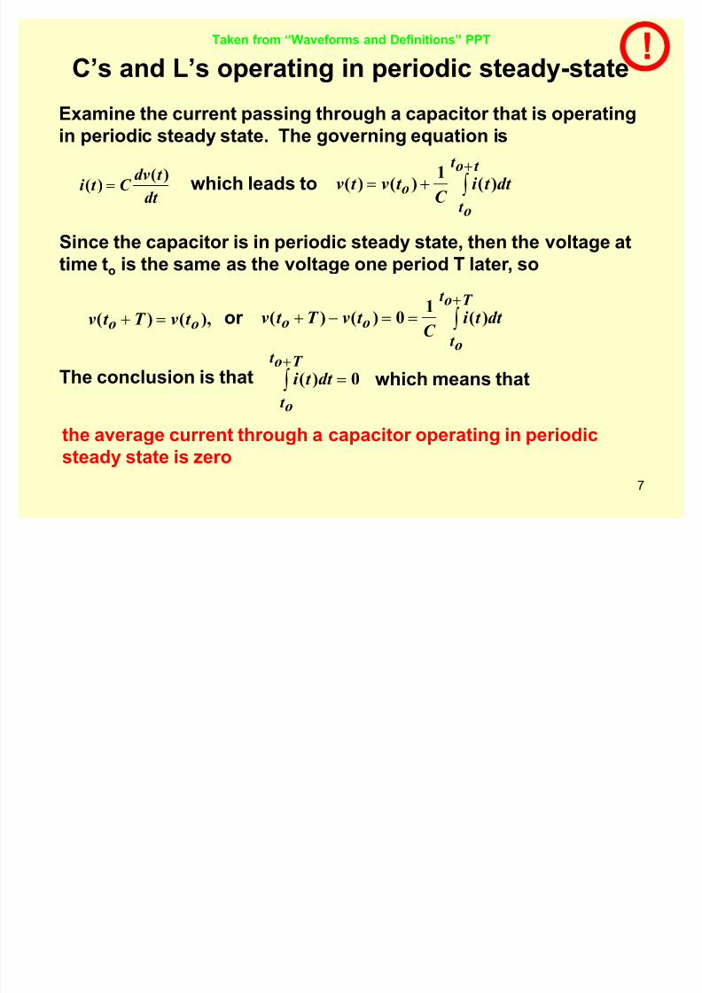
Examine the current passing through a capacitor that is operatingin periodic steady state. The governing equation is
dt t dv
C t i )(
)( ! which leads to ´!t ot
ot o dt t i
C t vt v )(
1)()(
Since the capacitor is in periodic steady state, then the voltage attime t o is the same as the voltage one period T later, so
),()( oo t vT t v !
The conclusion is that
´!!T ot
ot oo dt t i
C t vT t v )(
10)()(or
0)( !´T
ot
ot
dt t i
the average current through a capacitor operating in periodicsteady state is zero
which means that
Taken from ³Waveforms and Definitions´ PPT !

8/7/2019 _6_EE362L_DC_DC_Buck_PPT_Spring2009
http://slidepdf.com/reader/full/6ee362ldcdcbuckpptspring2009 8/38
8
N ow, an inductor
Examine the voltage across an inductor that is operating inperiodic steady state. The governing equation is
dt t di
Lt v)(
)( ! which leads to ´!t ot
ot o dt t v
Lt i t i )(
1)()(
Since the inductor is in periodic steady state, then the voltage attime t o is the same as the voltage one period T later, so
),()( oo t i T t i !
The conclusion is that
´!!T ot
ot oo dt t v
Lt i T t i )(
10)()(or
0)( !´T
ot
ot
dt t v
the average voltage across an inductor operating in periodicsteady state is zero
which means that
Taken from ³Waveforms and Definitions´ PPT !

8/7/2019 _6_EE362L_DC_DC_Buck_PPT_Spring2009
http://slidepdf.com/reader/full/6ee362ldcdcbuckpptspring2009 9/38
9
KVL and KCL in periodic steady-state
,0)(
!§l oopAround
t v
,0)(
!§n odeof O t
t i
0)()()()( 321 !t vt vt vt v N .
S ince KVL and KCL apply at any instance, t h en t h ey must also be validin averages. Consider KVL,
0)()()()( 321 !t i t i t i t i .
0)0(1)(1)(1)(1)(1321 !! ´´´´´ dt
T dt t v
T dt t v
T dt t v
T dt t v
T T o
t
ot
T ot
ot N
T ot
ot
T ot
ot
T ot
ot
.
0321 !Navg avg avg avg V V V V .
Th e same reasoning applies to KCL
0321 !avg avg avg avg I I I I .
KVL applies in the average sense
KCL applies in the average sense
Taken from ³Waveforms and Definitions´ PPT !
8/7/2019 _6_EE362L_DC_DC_Buck_PPT_Spring2009
http://slidepdf.com/reader/full/6ee362ldcdcbuckpptspring2009 10/38
10
Capacitors and Inductors
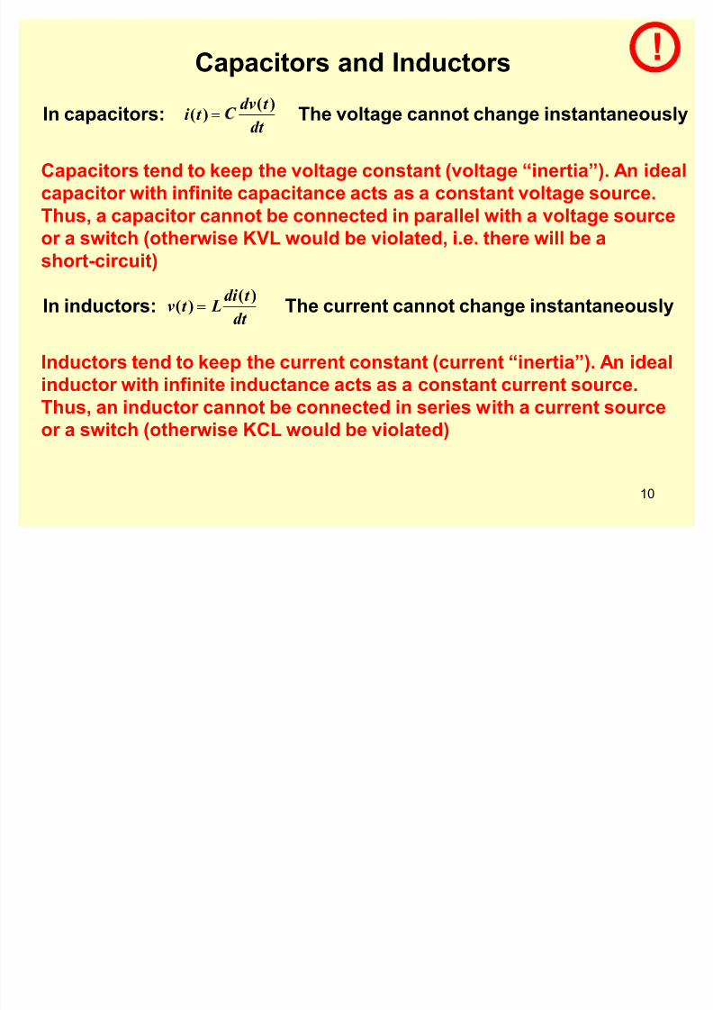
In capacitors:dt
t dvt i
)()( !
Capacitors tend to keep the voltage constant (voltage ³inertia´). An idealcapacitor with infinite capacitance acts as a constant voltage source.Thus, a capacitor cannot be connected in parallel with a voltage sourceor a switch (otherwise KVL would be violated, i.e. there will be ashort-circuit)
The voltage cannot change instantaneously
In inductors:
Inductors tend to keep the current constant (current ³inertia´). An idealinductor with infinite inductance acts as a constant current source.Thus, an inductor cannot be connected in series with a current sourceor a switch (otherwise KCL would be violated)
The current cannot change instantaneouslydt
t di Lt v
)()( !
!
8/7/2019 _6_EE362L_DC_DC_Buck_PPT_Spring2009
http://slidepdf.com/reader/full/6ee362ldcdcbuckpptspring2009 11/38
8/7/2019 _6_EE362L_DC_DC_Buck_PPT_Spring2009
http://slidepdf.com/reader/full/6ee362ldcdcbuckpptspring2009 12/38
12
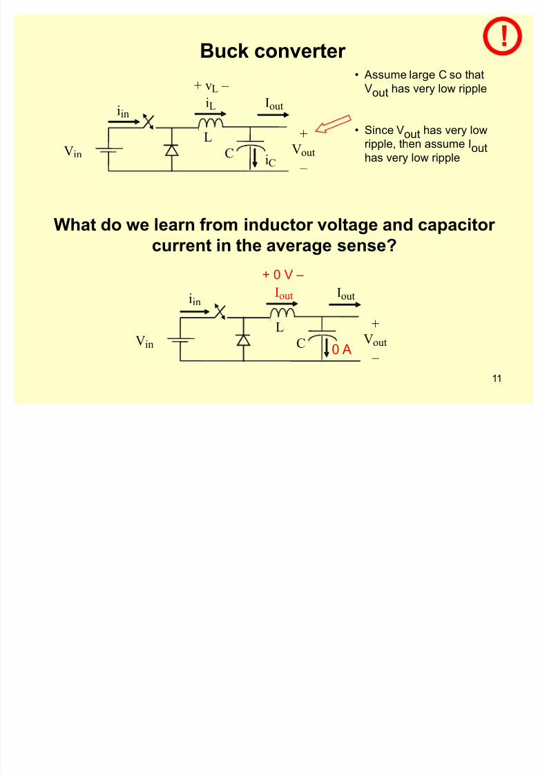
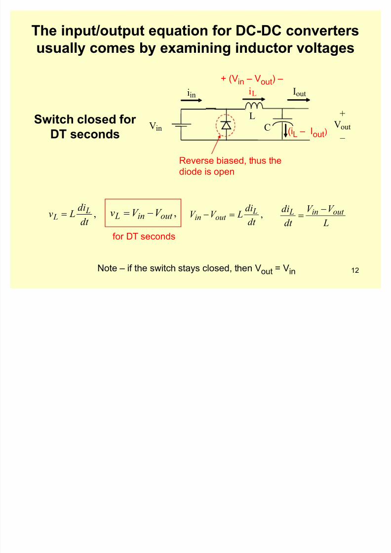
The input/output equation for DC-DC convertersusually comes by examining inductor voltages
Vin
+Vout
±
LC
Ioutiin
+ (V in ± Vout ) ±iL
(iL
± Iout
)
Reverse biased, t h us t h ediode is open
,d t
d iLv LL !
L
V V
d t
d i out inL !,d t
d iLV V L
out in !,out inL V V v !
f or D T seconds
Note ± i f th e switc h stays closed, t h en Vout
= Vin
Switch closed for
DT seconds

8/7/2019 _6_EE362L_DC_DC_Buck_PPT_Spring2009
http://slidepdf.com/reader/full/6ee362ldcdcbuckpptspring2009 13/38
13
Vin
+Vout
±
LC
Iout
± Vout +iL
(iL ± Iout )
Switch open for (1 í D)T seconds
iL continues to f low, t h us t h e diode is closed. Th isis t h e assumption o f ³continuous conduction´ in t h einductor w h ich is t h e normal operating condition.
,d t
d iv !
L
V
d t
d i out L !,d t
d iLV L
out !,out V v !
f or (1íD) T seconds

8/7/2019 _6_EE362L_DC_DC_Buck_PPT_Spring2009
http://slidepdf.com/reader/full/6ee362ldcdcbuckpptspring2009 14/38
14
Since the average voltage across L is zero
01 !yy! out out inLavg V DV V DV
out out out in V DV V DDV yy!
inout DV V !
From power balance, out out inin I V I V !
D
I I in
out !
, so
The input/output equation becomes
Note ± even t h oug h iin is not constant(i.e., i in h as h armonics), t h e input power is still simply V in Iin because V in h as noh armonics
!
8/7/2019 _6_EE362L_DC_DC_Buck_PPT_Spring2009
http://slidepdf.com/reader/full/6ee362ldcdcbuckpptspring2009 15/38
15
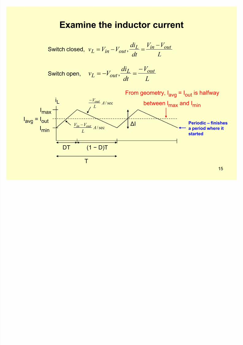
Examine the inductor current
S witc h closed,
S witc h open,
L
V V d t
d iV V v out inLout inL !! ,
L
V d t
d iV v out L
out L !! ,
sec/ AL
V V out in
DT (1 í D) T
T
Imax
Imin
Iavg = Iout
From geometry, I avg = Iout is h al f way
between I max and I minsec/ AL
V out
I
iL
Periodic ± finishes
a period where itstarted

8/7/2019 _6_EE362L_DC_DC_Buck_PPT_Spring2009
http://slidepdf.com/reader/full/6ee362ldcdcbuckpptspring2009 16/38
16
Effect of raising and lowering I out whileholding V in , Vout , f, and L constant
iL
I
IRaise I out
I
Lower I out
I is unc h anged
Lowering I out (and, t h ere f ore, P out ) moves t h e circuittoward discontinuous operation
8/7/2019 _6_EE362L_DC_DC_Buck_PPT_Spring2009
http://slidepdf.com/reader/full/6ee362ldcdcbuckpptspring2009 17/38
17
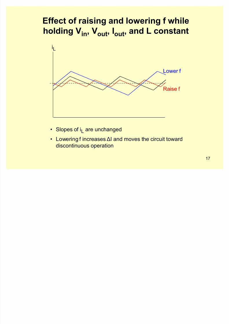
Effect of raising and lowering f whileholding V in , Vout , Iout , and L constant
iL
Raise f
Lower f
S lopes o f iL are unc h anged
Lowering f increases I and moves t h e circuit towarddiscontinuous operation
8/7/2019 _6_EE362L_DC_DC_Buck_PPT_Spring2009
http://slidepdf.com/reader/full/6ee362ldcdcbuckpptspring2009 18/38
18
iL
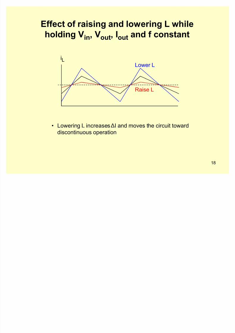
Effect of raising and lowering L whileholding V in , Vout , Iout and f constant
Raise L
Lower L
Lowering L increases I and moves t h e circuit towarddiscontinuous operation
8/7/2019 _6_EE362L_DC_DC_Buck_PPT_Spring2009
http://slidepdf.com/reader/full/6ee362ldcdcbuckpptspring2009 19/38
19
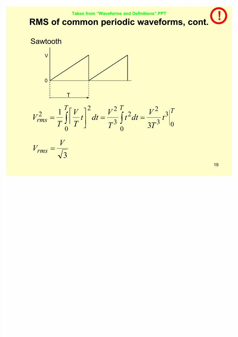
RMS of common periodic waveforms, cont.
T T T
rms t T
V d t t
T
V d t t
T
V
T
V
0
3
3
2
0
2
3
2
0
22
3
1!!¼
½
»¬«!
´´
T
V
0
3
V V rms !
S awtoot h
Taken from ³Waveforms and Definitions´ PPT !

8/7/2019 _6_EE362L_DC_DC_Buck_PPT_Spring2009
http://slidepdf.com/reader/full/6ee362ldcdcbuckpptspring2009 20/38
20
RMS of common periodic waveforms, cont.Using t h e power concept, it is easy to reason t h at t h e f ollowing wave f ormswould all produce t h e same average power to a resistor, and t h us t h eir rmsvalues are identical and equal to t h e previous example
V
0
V
0
V
0
0
-V
V
0
3
V V rms !
V
0
V
0
Taken from ³Waveforms and Definitions´ PPT !

8/7/2019 _6_EE362L_DC_DC_Buck_PPT_Spring2009
http://slidepdf.com/reader/full/6ee362ldcdcbuckpptspring2009 21/38
21
RMS of common periodic waveforms, cont.Now, consider a use f ul example, based upon a wave f orm t h at is o f ten seen inDC-DC converter currents. Decompose t h e wave f orm into its ripple, plus itsminimum value.
minmax I I
0
)(t i(th e ripple
+
0
minI
th e minimum value
)(t imaI
minI =
2
mima I I I avg !
avg I
Taken from ³Waveforms and Definitions´ PPT !

8/7/2019 _6_EE362L_DC_DC_Buck_PPT_Spring2009
http://slidepdf.com/reader/full/6ee362ldcdcbuckpptspring2009 22/38
22
RMS of common periodic waveforms, cont.
_ a2
m in2
)( I t iA vg I rms ! (
_ a2m inm in
22)(2)( I I t it iAvg I r s y! ((
_ a _ a 2m inm in22 )( 2)( I t iAvg I t iAvg I rms y! ((
2m in
m inmaxm in
2m inmax2
22
3I
I I I
I I I r s y!
2m inm in
22
3I I I
I I PP
PP r s !
m inmax I I I PP !De f ine
Taken from ³Waveforms and Definitions´ PPT
8/7/2019 _6_EE362L_DC_DC_Buck_PPT_Spring2009
http://slidepdf.com/reader/full/6ee362ldcdcbuckpptspring2009 23/38
23
RMS of common periodic waveforms, cont.
2m in PP avg
I I I !
222
223¹º¸©
ª¨¹
º¸©
ª¨! PP
avg PP PP
avg PP
rmsI
I I I
I I
I
423
22
222 PP
PP avg avg PP
PP avg PP
rmsI
I I I I
I I I
I !
222
2
43 avg PP PP
r s I I I
I !
Recognize t h at
12
222 PP avg rms
I I I !
avg I
)(t i
m inmax I I I PP !
2
m inmax I I I avg !
Taken from ³Waveforms and Definitions´ PPT

8/7/2019 _6_EE362L_DC_DC_Buck_PPT_Spring2009
http://slidepdf.com/reader/full/6ee362ldcdcbuckpptspring2009 24/38
24
Inductor current rating
22222
12
1
12
1I I I I I out ppavg Lrms (!!
2222
342
12
1out out out Lr s I I I I !! (
M ax impact o f I on t h e rms current occurs at t h e boundary o f continuous/discontinuous conduction, w h ere I =2Iout
out Lr s I I 3
2!
2Iout
0
Iavg = Iout I
iL
Use max

8/7/2019 _6_EE362L_DC_DC_Buck_PPT_Spring2009
http://slidepdf.com/reader/full/6ee362ldcdcbuckpptspring2009 25/38
25
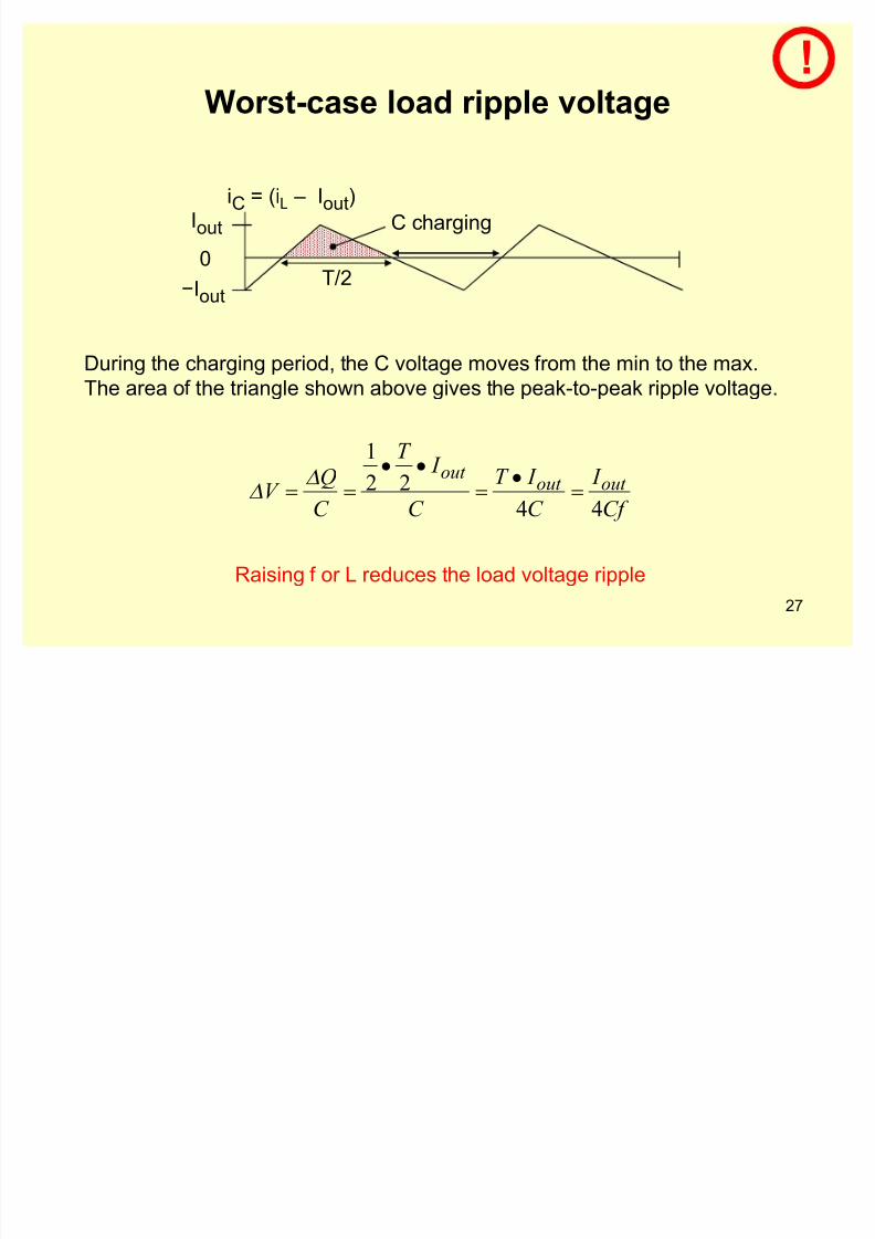
Capacitor current and current rating
22222
3
102
12
1out out avg C r s I I I I !!
iL
LC
Iout
(iL ± Iout )
Iout
íI out
0I
M ax rms current occurs at t h e boundary o f continuous/discontinuousconduction, w h ere I =2I
out
3out
rmsI
I !
Use max
iC = (iL ± Iout ) Note ± raising f or L, w h ich lowersI, reduces t h e capacitor current

8/7/2019 _6_EE362L_DC_DC_Buck_PPT_Spring2009
http://slidepdf.com/reader/full/6ee362ldcdcbuckpptspring2009 26/38
26
MOSFET and diode currents and current ratingsiL
LC
Iout
(iL ± Iout )
out rms I I 3
2!
Use max
2Iout
0
Iout
iin
2Iout
0
Iout
Take worst case D f or eac h
8/7/2019 _6_EE362L_DC_DC_Buck_PPT_Spring2009
http://slidepdf.com/reader/full/6ee362ldcdcbuckpptspring2009 27/38
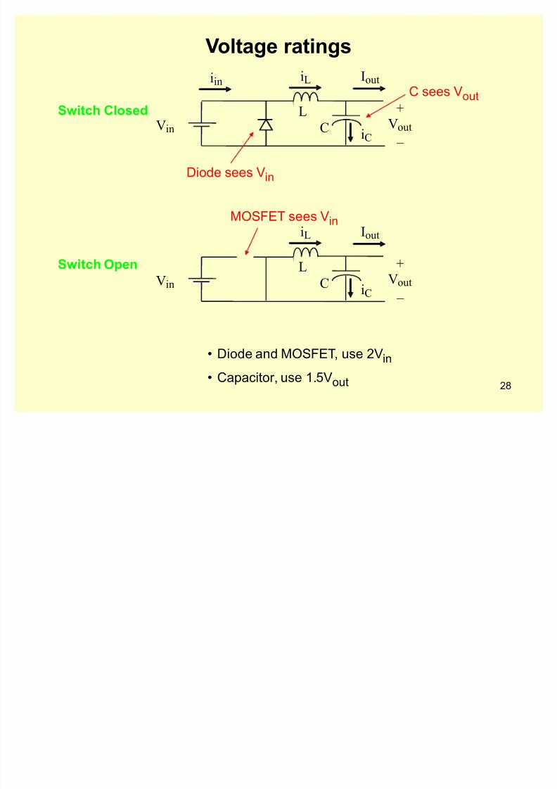
8/7/2019 _6_EE362L_DC_DC_Buck_PPT_Spring2009
http://slidepdf.com/reader/full/6ee362ldcdcbuckpptspring2009 28/38
28
Vin
+Vout
±
iL
LC
iC
Iout
Vin
+Vout
±
iL
LC iC
Ioutiin
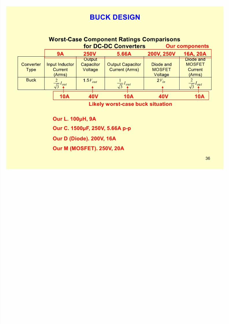
Voltage ratings
Diode sees V in
MOS FE T sees V in
C sees Vout
Diode and MOS FE T, use 2V in
Capacitor, use 1. 5 Vout
Switch Closed
Switch Open

8/7/2019 _6_EE362L_DC_DC_Buck_PPT_Spring2009
http://slidepdf.com/reader/full/6ee362ldcdcbuckpptspring2009 29/38
29
There is a 3 rd state ± discontinuous
Vin
+Vout
±
LC
Iout
O ccurs f or lig h t loads, or low operating f requencies, w h ereth e inductor current eventually h its zero during t h e switc h -open state
Th e diode opens to prevent backward current f low
Th e small capacitances o f th e MOS FE T and diode, acting inparallel wit h eac h oth er as a net parasitic capacitance,interact wit h L to produce an oscillation
Th e output C is in series wit h th e net parasitic capacitance,but C is so large t h at it can be ignored in t h e oscillationph enomenon
Iout
MOSFE
T
DIO DE
!

8/7/2019 _6_EE362L_DC_DC_Buck_PPT_Spring2009
http://slidepdf.com/reader/full/6ee362ldcdcbuckpptspring2009 30/38
30
Inductor voltage showing oscillation duringdiscontinuous current operation
} 65 0kHz. Wit h L = 100µH, t h is correspondsto net parasitic C = 0. 6 nF
vL = (V in ± Vout )
vL = ±V out
Switch open
Switchclosed
8/7/2019 _6_EE362L_DC_DC_Buck_PPT_Spring2009
http://slidepdf.com/reader/full/6ee362ldcdcbuckpptspring2009 31/38
31
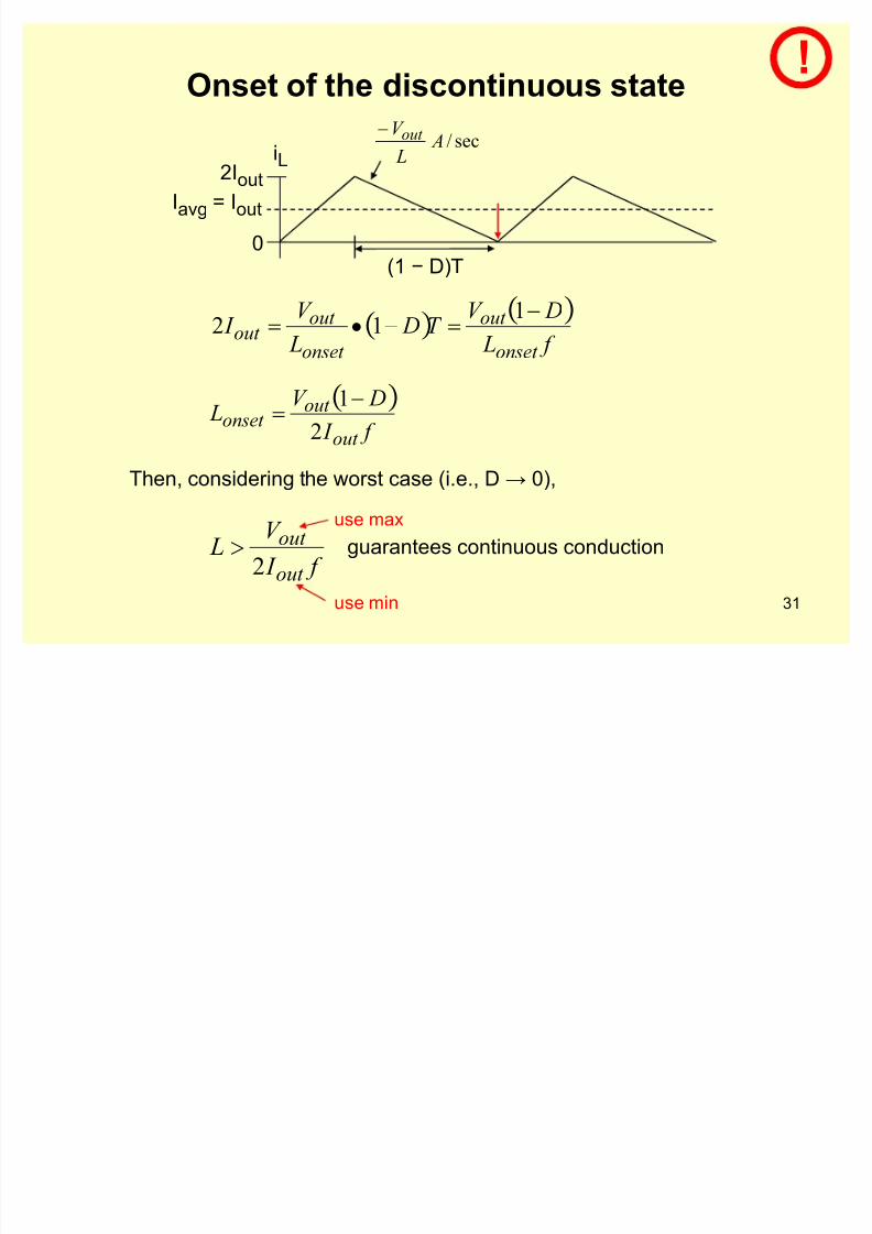
Onset of the discontinuous state
sec/ AL
V out
f LDV T D
LV I
on se t
out
on se t
out out !y! 112
2Iout
0
Iavg = Iout
iL
(1 í D) T
f I
V L
out
out 2
" guarantees continuous conductionuse max
use min
f I
DV L
out
out on se t 2
1!
Th en, considering t h e worst case (i.e., D 0),
!

8/7/2019 _6_EE362L_DC_DC_Buck_PPT_Spring2009
http://slidepdf.com/reader/full/6ee362ldcdcbuckpptspring2009 32/38
32
Impedance matching
out
out l oad I
V R !
equivR
DCíDC BuckConverter
+
Vin
í
+
Vout = DV in
í
Iout = Iin / DIin
+
Vin
í
Iin
22 D
R
DI
V DI
D
V
I V
R l oad
out
out
out
out
in
inequiv !
y!
y!!
Equivalent f romsource perspective
S ource
So, the buck converter makes the loadresistance look larger to the source
!
8/7/2019 _6_EE362L_DC_DC_Buck_PPT_Spring2009
http://slidepdf.com/reader/full/6ee362ldcdcbuckpptspring2009 33/38
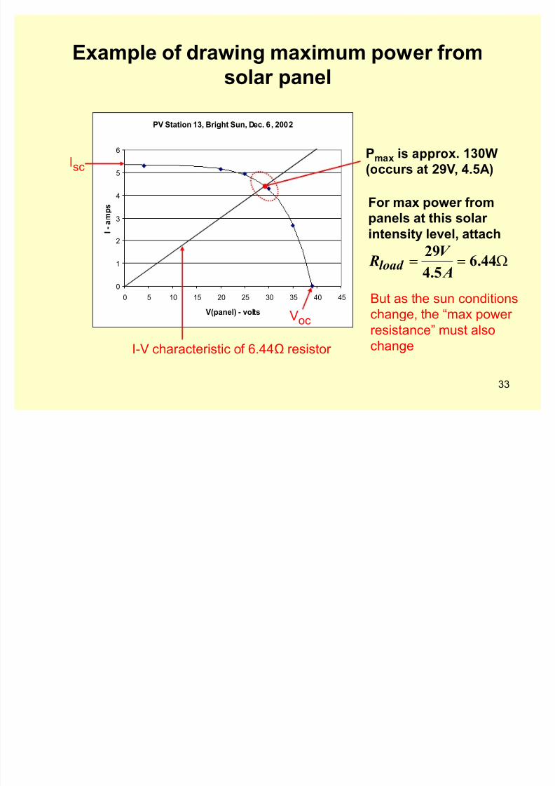
33
Example of drawing maximum power fromsolar panel
PV Station 13, Bright Sun, Dec. 6 , 2002
0
1
2
3
4
5
6
0 5 10 15 20 25 30 35 40 45
V(panel) - volts
I - amps
Isc
Voc
P ma x is app r o x. 130W (o ccur s at 29 V, 4.5A )
;!! 44.65.4
29A
V Rl oad
For max power frompanels at this solar intensity level, attach
I-V ch aracteristic o f 6 .44 resistor
But as t h e sun conditionsch ange, t h e ³max power resistance´ must alsoch ange
8/7/2019 _6_EE362L_DC_DC_Buck_PPT_Spring2009
http://slidepdf.com/reader/full/6ee362ldcdcbuckpptspring2009 34/38
34
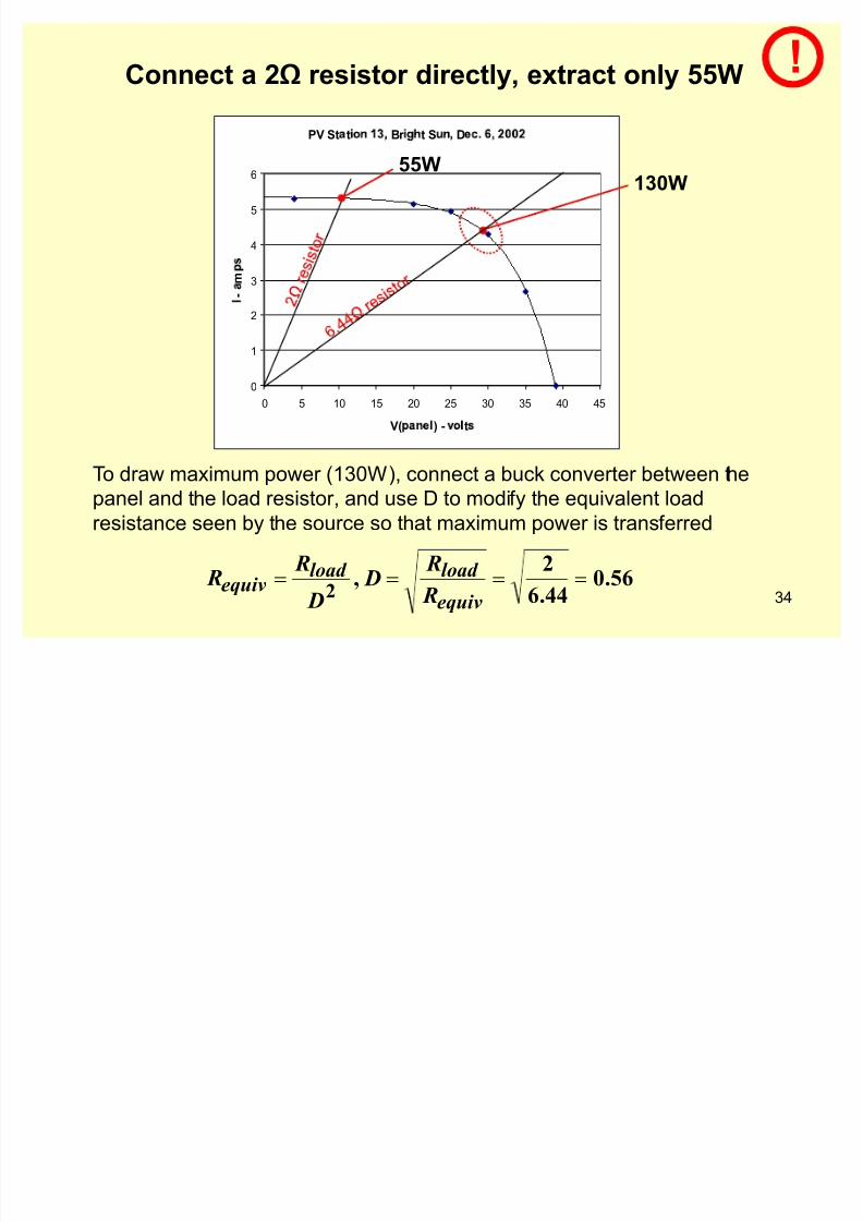
Connect a 2 resistor directly, extract only 55W
PV St t Br t S D
0
1
2
3
4
5
6
0 5 10 15 20 25 30 35 40 45
V( ) - t
-m
130W55W
56.044.6
2 ,
2!!!!
equiv
l oad l oad equiv R
RD
D
RR
To draw maximum power (130W), connect a buck converter between t h epanel and t h e load resistor, and use D to modi f y th e equivalent loadresistance seen by t h e source so t h at maximum power is trans f erred
!
8/7/2019 _6_EE362L_DC_DC_Buck_PPT_Spring2009
http://slidepdf.com/reader/full/6ee362ldcdcbuckpptspring2009 35/38
8/7/2019 _6_EE362L_DC_DC_Buck_PPT_Spring2009
http://slidepdf.com/reader/full/6ee362ldcdcbuckpptspring2009 36/38

8/7/2019 _6_EE362L_DC_DC_Buck_PPT_Spring2009
http://slidepdf.com/reader/full/6ee362ldcdcbuckpptspring2009 37/38
37
Comp a ris on s o Ou tpu t Ca p ac itor Rippl e Vol ta g e
Con ve r te r T p e Vol ts p eak-t o -p eak) Bu ck
Cf
I out 4
10A
1500µF 50kHz
0.033V
BUC K DESIG N
Our M (M OSFET). 250V, 20A
Our L. 100µH, 9AOur C. 1500µF, 250V, 5.66A p-p
Our D (Diode). 200V, 16A

8/7/2019 _6_EE362L_DC_DC_Buck_PPT_Spring2009
http://slidepdf.com/reader/full/6ee362ldcdcbuckpptspring2009 38/38
38
Minimum Induc t nce Values Needed t Guaran tee Con tinuous Curren t
Conver ter Type For Con tinuousCurren t in th e Inpu t
Induc tor
For Con tinuousCurren t in L2
Buckf I
V Lout
out 2
" ±40V
2A 50kHz
200µH
BUC K DESIG N
Our M (M OSFET). 250V, 20A
Our L. 100µH, 9AOur C. 1500µF, 250V, 5.66A p-p
Our D (Diode). 200V, 16A