Data Sheet Broadcom AV02-0171EN January 30, 2019 Description These diode-transistor optocouplers use an insulating layer between a LED and an integrated photodetector to provide electrical insulation between input and output. Separate connections for the photodiode bias and output-transistor collector increase the speed up to a hundred times that of a conventional phototransistor coupler by reducing the base-collector capacitance. These single channel optocoup-lers are available in 8-pin DIP, SO-8, and Widebody package configurations. The 6N135, HCPL-0500, and HCNW135 are for use in TTL/CMOS, TTL/LSTTL or wide-bandwidth analog applications. Current transfer ratio (CTR) for these devices is 7% minimum at I F = 16 mA. The 6N136, HCPL-2502, HCPL-0501, and HCNW136 are designed for high-speed TTL/TTL applications. A standard 16-mA TTL sink current through the input LED will provide enough output current for 1 TTL load and a 5.6 kpull-up resistor. CTR for these devices is 19% minimum at I F = 16 mA. Features High speed: 1 Mb/s TTL compatible Available in 8-pin DIP, SO-8, widebody packages Open collector output Safety approval UL Recognized – 3750 V rms for 1 minute (5000 V rms for 1 minute for HCNW and Option 020 devices) per UL1577 CSA Approved IEC/EN/DIN EN 60747-5-5 Approved – V IORM = 567V peak for SO-8 devices – V IORM = 630V peak for DIP 300 mil devices – V IORM = 1414V peak for DIP 400 mil (widebody) devices Dual channel version available (253X/053X/0534) Applications High voltage insulation Video signal isolation Line receivers Feedback element in switched mode power supplies High speed logic ground isolation – TTL/TTL, TTL/CMOS, TTL/LSTTL Replaces pulse transformers Replaces slow phototransistor isolators Analog signal ground isolation CAUTION! Take normal static precautions in handling and assembly of this component to prevent damage and/or degradation that may be induced by ESD. 6N135/6, HCNW135/6, HCPL-2502/0500/ 0501 Single-Channel, High-Speed Optocouplers
These diode-transistor optocouplers use an insulating layer between a LED and an integrated photodetector to provide electrical insulation between input and output. Separate connections for the photodiode bias and output-transistor collector increase the speed up to a hundred times that of a conventional phototransistor coupler by reducing the base-collector capacitance.
These single channel optocoup-lers are available in 8-pin DIP, SO-8, and Widebody package configurations.
The 6N135, HCPL-0500, and HCNW135 are for use in TTL/CMOS, TTL/LSTTL or wide-bandwidth analog applications. Current transfer ratio (CTR) for these devices is 7% minimum at IF = 16 mA.
The 6N136, HCPL-2502, HCPL-0501, and HCNW136 are designed for high-speed TTL/TTL applications. A standard 16-mA TTL sink current through the input LED will provide enough output current for 1 TTL load and a 5.6 k pull-up resistor. CTR for these devices is 19% minimum at IF = 16 mA.
Features High speed: 1 Mb/s
TTL compatible
Available in 8-pin DIP, SO-8, widebody packages
Open collector output
Safety approval
UL Recognized – 3750 Vrms for 1 minute (5000 Vrms for 1 minute for HCNW and Option 020 devices) per UL1577
CSA Approved
IEC/EN/DIN EN 60747-5-5 Approved
– VIORM = 567V peak for SO-8 devices
– VIORM = 630V peak for DIP 300 mil devices
– VIORM = 1414V peak for DIP 400 mil (widebody) devices
Dual channel version available (253X/053X/0534)
Applications High voltage insulation
Video signal isolation
Line receivers
Feedback element in switched mode power supplies
High speed logic ground isolation
– TTL/TTL, TTL/CMOS, TTL/LSTTL
Replaces pulse transformers
Replaces slow phototransistor isolators
Analog signal ground isolation
CAUTION! Take normal static precautions in handling and assembly of this component to prevent damage and/or degradation that may be induced by ESD.
Broadcom AV02-0171ENJanuary 30, 2019
6N135/6, HCNW135/6, HCPL-2502/0500/0501 Data Sheet Single-Channel, High-Speed Optocouplers
Functional Diagram
Truth Table (Positive Logic)
A 0.1-µF bypass capacitor must be connected between pins 5 and 8.
6N135/6, HCNW135/6, HCPL-2502/0500/0501 Data Sheet Single-Channel, High-Speed Optocouplers
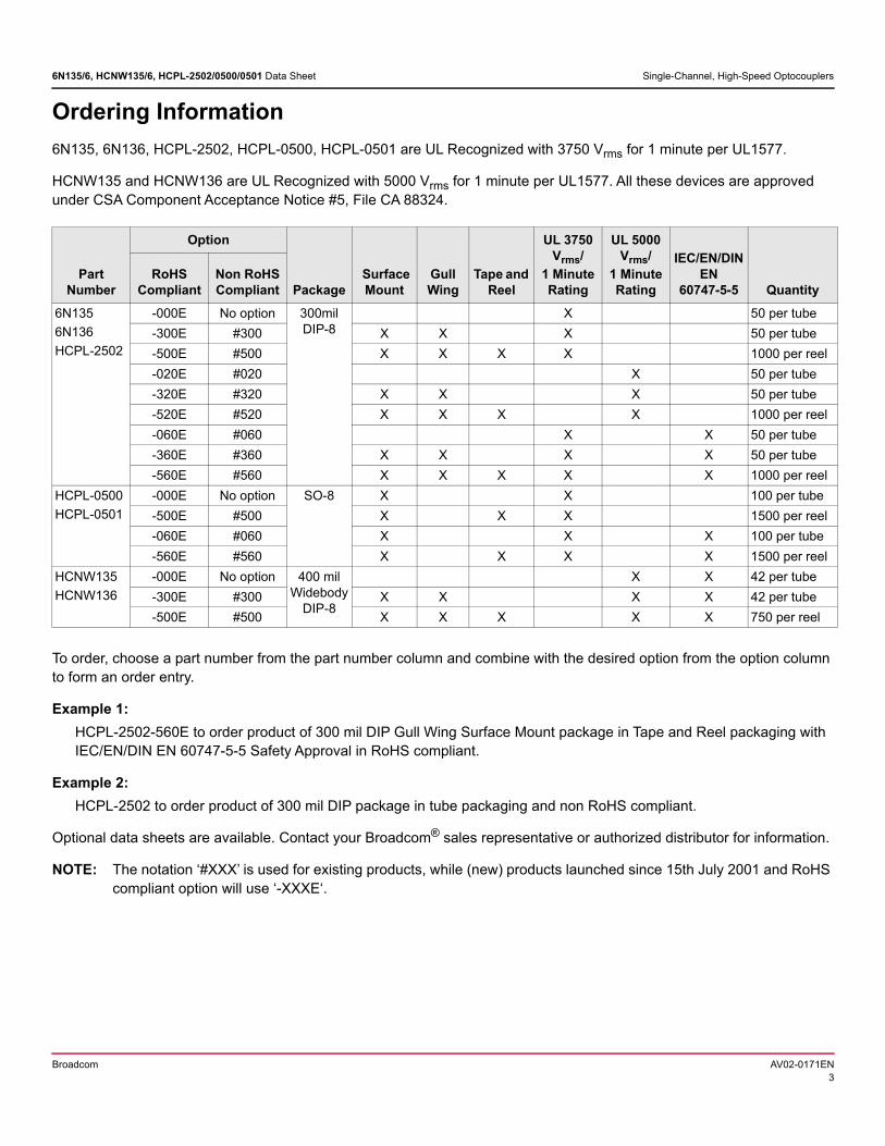
Ordering Information
6N135, 6N136, HCPL-2502, HCPL-0500, HCPL-0501 are UL Recognized with 3750 Vrms for 1 minute per UL1577.
HCNW135 and HCNW136 are UL Recognized with 5000 Vrms for 1 minute per UL1577. All these devices are approved under CSA Component Acceptance Notice #5, File CA 88324.
To order, choose a part number from the part number column and combine with the desired option from the option column to form an order entry.
Example 1:
HCPL-2502-560E to order product of 300 mil DIP Gull Wing Surface Mount package in Tape and Reel packaging with IEC/EN/DIN EN 60747-5-5 Safety Approval in RoHS compliant.
Example 2:
HCPL-2502 to order product of 300 mil DIP package in tube packaging and non RoHS compliant.
Optional data sheets are available. Contact your Broadcom® sales representative or authorized distributor for information.
NOTE: The notation ‘#XXX’ is used for existing products, while (new) products launched since 15th July 2001 and RoHS compliant option will use ‘-XXXE‘.
Part Number
Option
Package Surface Mount
Gull Wing
Tape and Reel
UL 3750 Vrms/
1 Minute Rating
UL 5000 Vrms/
1 Minute Rating
IEC/EN/DIN EN
60747-5-5 QuantityRoHS
CompliantNon RoHS Compliant
6N135
6N136
HCPL-2502
-000E No option 300mil DIP-8
X 50 per tube
-300E #300 X X X 50 per tube
-500E #500 X X X X 1000 per reel
-020E #020 X 50 per tube
-320E #320 X X X 50 per tube
-520E #520 X X X X 1000 per reel
-060E #060 X X 50 per tube
-360E #360 X X X X 50 per tube
-560E #560 X X X X X 1000 per reel
HCPL-0500
HCPL-0501
-000E No option SO-8 X X 100 per tube
-500E #500 X X X 1500 per reel
-060E #060 X X X 100 per tube
-560E #560 X X X X 1500 per reel
HCNW135
HCNW136
-000E No option 400 mil Widebody
DIP-8
X X 42 per tube
-300E #300 X X X X 42 per tube
-500E #500 X X X X X 750 per reel
Broadcom AV02-0171EN3
6N135/6, HCNW135/6, HCPL-2502/0500/0501 Data Sheet Single-Channel, High-Speed Optocouplers
Package Outline Drawings
8-Pin DIP Package (6N135/6, HCPL-2502)
1.080 ± 0.320(0.043 ± 0.013)
2.54 ± 0.25(0.100 ± 0.010)
0.51 (0.020) MIN.
0.65 (0.025) MAX.
4.70 (0.185) MAX.
2.92 (0.115) MIN.
5 TYP. 0.254+ 0.076- 0.051
(0.010+ 0.003)- 0.002)
7.62 ± 0.25(0.300 ± 0.010)
6.35 ± 0.25(0.250 ± 0.010)
9.65 ± 0.25(0.380 ± 0.010)
1.78 (0.070) MAX.1.19 (0.047) MAX.
A XXXXZYYWW
DATE CODE
DIMENSIONS IN MILLIMETERS AND (INCHES).
5678
4321
OPTION CODE*
UL RECOGNITION
UR
TYPE NUMBER
*MARKING CODE LETTER FOR OPTION NUMBERS"L" = OPTION 020"V" = OPTION 060OPTION NUMBERS 300 AND 500 NOT MARKED.
NOTE: FLOATING LEAD PROTRUSION IS 0.25 mm (10 mils) MAX.
3.56 ± 0.13(0.140 ± 0.005)
LOT ID
EEE
Broadcom AV02-0171EN4
6N135/6, HCNW135/6, HCPL-2502/0500/0501 Data Sheet Single-Channel, High-Speed Optocouplers
8-Pin DIP Package with Gull Wing Surface Mount Option 300 (6N135/6)
0.635 ± 0.25(0.025 ± 0.010)
12 NOM.
9.65 ± 0.25(0.380 ± 0.010)
0.635 ± 0.130(0.025 ± 0.005)
7.62 ± 0.25(0.300 ± 0.010)
5678
4321
9.65 ± 0.25(0.380 ± 0.010)
6.350 ± 0.25(0.250 ± 0.010)
1.016 (0.040)
1.27 (0.050)
10.9 (0.430)
2.0 (0.080)
LAND PATTERN RECOMMENDATION
1.080 ± 0.320(0.043 ± 0.013)
3.56 ± 0.13(0.140 ± 0.005)
1.780(0.070)
MAX.1.19
(0.047)MAX.
2.54(0.100)
BSCDIMENSIONS IN MILLIMETERS (INCHES).LEAD COPLANARITY = 0.10 mm (0.004 INCHES).
NOTE: FLOATING LEAD PROTRUSION IS 0.25 mm (10 mils) MAX.
0.254+ 0.076- 0.051
(0.010+ 0.003)- 0.002)
Broadcom AV02-0171EN5
6N135/6, HCNW135/6, HCPL-2502/0500/0501 Data Sheet Single-Channel, High-Speed Optocouplers
Small Outline SO-8 Package (HCPL-0500/1)
XXXYWW
4321
5.994 ± 0.203(0.236 ± 0.008)
3.937 ± 0.127(0.155 ± 0.005)
0.406 ± 0.076(0.016 ± 0.003) 1.270
(0.050)BSC
5.080 ± 0.127(0.200 ± 0.005)
3.175 ± 0.127(0.125 ± 0.005) 1.524
(0.060)
45 X0.432
(0.017)
0.228 ± 0.025(0.009 ± 0.001)
TYPE NUMBER(LAST 3 DIGITS)DATE CODE
0.305(0.012)
MIN.
TOTAL PACKAGE LENGTH (INCLUSIVE OF MOLD FLASH)5.207 ± 0.254 (0.205 ± 0.010)
DIMENSIONS IN MILLIMETERS (INCHES).LEAD COPLANARITY = 0.10 mm (0.004 INCHES) MAX.
0.203 ± 0.102(0.008 ± 0.004)
7
PIN ONE
0 ~ 7
*
*
7.49 (0.295)
1.9 (0.075)
0.64 (0.025)
LAND PATTERN RECOMMENDATION
5678
LOT ID
EEE
Broadcom AV02-0171EN6
6N135/6, HCNW135/6, HCPL-2502/0500/0501 Data Sheet Single-Channel, High-Speed Optocouplers
8-Pin Widebody DIP Package (HCNW135/6)
5678
4321
11.23 ± 0.15(0.442 ± 0.006)
1.8 ± 0.15(0.071 ± 0.006)
5.10(0.201)
MAX.
1.55(0.061)
MAX.
2.54 (0.100)TYP. DIMENSIONS IN MILLIMETERS (INCHES).
NOTE: FLOATING LEAD PROTRUSION IS 0.25 mm (10 mils) MAX.
7 TYP.0.254
+ 0.076- 0.0051
(0.010+ 0.003)- 0.002)
11.00(0.433)
9.00 ± 0.15(0.354 ± 0.006)
MAX.
10.16 (0.400)TYP.
AHCNWXXXX
YYWW
DATE CODE
TYPE NUMBER
0.51 (0.021) MIN.
0.40 (0.016)0.56 (0.022)
3.10 (0.122)3.90 (0.154)
LOT ID
EEE
Broadcom AV02-0171EN7
6N135/6, HCNW135/6, HCPL-2502/0500/0501 Data Sheet Single-Channel, High-Speed Optocouplers
8-Pin Widebody DIP Package with Gull Wing Surface Mount Option 300 (HCNW135/6)
Solder Reflow Profile
Recommended reflow conditions are as per JEDEC Standard, J-STD-020 (latest revision). Non-halide flux should be used.
Regulatory Information
The devices contained in this data sheet have been approved by the following organizations:
UL Approval under UL 1577, Component Recognition Program, File E55361.
CSA Approval under CSA Component Acceptance Notice #5, File CA 88324.
IEC/EN/DIN EN 60747-5-5 (HCNW and Option 060/360/560 only)
1.00 ± 0.15(0.039 ± 0.006)
7 NOM.
12.30 ± 0.30(0.484 ± 0.012)
0.75 ± 0.25(0.030 ± 0.010)
11.00(0.433)
5678
4321
11.23 ± 0.15(0.442 ± 0.006)
9.00 ± 0.15(0.354 ± 0.006)
1.3(0.051)
13.56(0.534)
2.29(0.09)
LAND PATTERN RECOMMENDATION
1.80 ± 0.15(0.071 ± 0.006)
4.00(0.158)
MAX.
1.55(0.061)
MAX.
2.54(0.100)
BSC
DIMENSIONS IN MILLIMETERS (INCHES).
LEAD COPLANARITY = 0.10 mm (0.004 INCHES).
NOTE: FLOATING LEAD PROTRUSION IS 0.25 mm (10 mils) MAX.
0.254+ 0.076
- 0.0051
(0.010+ 0.003)- 0.002)
MAX.
Broadcom AV02-0171EN8
6N135/6, HCNW135/6, HCPL-2502/0500/0501 Data Sheet Single-Channel, High-Speed Optocouplers
Insulation and Safety Related Specifications
Option 300 – Surface mount classification is Class A in accordance with CECC 00802.
Parameter Symbol
8-Pin DIP (300 Mil)
Value SO-8 Value
Widebody (400 Mil)
Value Units Conditions
Minimum External Air Gap (External Clearance)
L(101) 7.1 4.9 9.6 mm Measured from input terminals to output terminals, shortest distance through air.
Minimum External Tracking (External Creepage)
L(102) 7.4 4.8 10.0 mm Measured from input terminals to output terminals, shortest distance path along body..
Minimum Internal Plastic Gap(Internal Clearance)
0.08 0.08 1.0 mm Through insulation distance conductor to conductor, usually the direct distance between the photoemitter and photodetector inside the optocoupler cavity.
Minimum Internal Tracking (Internal Creepage)
N/A N/A 4.0 mm Measured from input terminals to output terminals, along internal cavity.
Tracking Resistance(Comparative Tracking Index)
CTI 200 200 200 V DIN IEC 112/VDE 0303 Part 1
Isolation Group IIIa IIIa IIIa Material Group (DIN VDE 0110, 1/89, Table 1)
Broadcom AV02-0171EN9
6N135/6, HCNW135/6, HCPL-2502/0500/0501 Data Sheet Single-Channel, High-Speed Optocouplers
IEC/EN/DIN EN 60747-5-5 Insulation Characteristicsa (Option 060 Only)
NOTE: Isolation characteristics are guaranteed only within the safety maximum ratings, which must be ensured by protective circuits in the application.
Description Symbol 8-Pin DIP SO-8 Units
Installation Classification per DIN VDE 0110/39, Table 1
for rated mains voltage 150 Vrms
for rated mains voltage 300 Vrms
for rated mains voltage 600 Vrms
I – IV
I – IV
I – IV
I – IV
I – IV
I – III
Climatic Classification 0/70/21 0/70/21
Pollution Degree (DIN VDE 0110/39) 2 2
Maximum Working Insulation Voltage VIORM 630 567 Vpeak
Input to Output Test Voltage, Method ba
VIORM × 1.875 = VPR, 100% Production Test with tm = 1s, Partial Discharge < 5 pC
a. Refer to the front of the optocoupler section of the current catalog, under Product Safety Regulations section IEC/EN/DIN EN 60747-5-5, for a detailed description.
VPR 1181 1063 Vpeak
Input to Output Test Voltage, Method aa
VIORM x 1.6 = VPR, Type and Sample Test, tm = 10s, Partial Discharge < 5 pC
Safety-limiting values – Maximum Values Allowed in the Event of a Failure
Case TemperatureInput CurrentOutput Power
TS
IS, INPUT
PS, OUTPUT
175
230
600
150
150
600
°C
mA
mW
Insulation Resistance at TS, VIO = 500V RS ≥109 ≥109
Broadcom AV02-0171EN10
6N135/6, HCNW135/6, HCPL-2502/0500/0501 Data Sheet Single-Channel, High-Speed Optocouplers
IEC/EN/DIN EN 60747-5-5 Insulation Characteristicsa (HCNW135/6 Option 060 Only)
NOTE: Isolation characteristics are guaranteed only within the safety maximum ratings, which must be ensured by protective circuits in the application.
Description Symbol Characteristic Units
Installation Classification per DIN VDE 0110/39, Table 1
for rated mains voltage 150 Vrms
for rated mains voltage 300 Vrms
for rated mains voltage 600 Vrms
for rated mains voltage 1000 Vrms
I – IV
I – IV
I – IV
I – III
Climatic Classification 0/70/21
Pollution Degree (DIN VDE 0110/39) 2
Maximum Working Insulation Voltage VIORM 1414 Vpeak
Input to Output Test Voltage, Method ba
VIORM × 1.875 = VPR, 100% Production Test with tm = 1s, Partial Discharge < 5 pC
a. Refer to the front of the optocoupler section of the current catalog, under Product Safety Regulations section IEC/EN/DIN EN 60747-5-5, for a detailed description.
VPR 2651 Vpeak
Input to Output Test Voltage, Method aa
VIORM x 1.6 = VPR, Type and Sample Test, tm = 10s, Partial Discharge < 5 pC
Safety-limiting values – Maximum Values Allowed in the Event of a Failure
Case TemperatureInput CurrentOutput Power
TS
IS, INPUT
PS, OUTPUT
150
400
700
°C
mA
mW
Insulation Resistance at TS, VIO = 500V RS ≥109
Broadcom AV02-0171EN11
6N135/6, HCNW135/6, HCPL-2502/0500/0501 Data Sheet Single-Channel, High-Speed Optocouplers
Absolute Maximum Rating
Parameter Symbol Device Min. Max. Units Note
Storage Temperaturea
a. Data has been registered with JEDEC for the 6N135/6N136.
TS –55 125 °C
Operating Temperaturea TA 8-Pin DIP SO-8 –55 100 °C
Widebody –55 85
Average Forward Input Currenta IF(AVG) — 25 mA b
b. Derate linearly above 70°C free-air temperature at a rate of 0.8 mA/°C (8-Pin DIP). Derate linearly above 85°C free-air temperature at a rate of 0.5 mA/°C (SO-8).
Peak Forward Input Currenta
(50% duty cycle, 1-ms pulse width)
IF(PEAK) 8-Pin DIP SO-8 — 50 mA c
c. Derate linearly above 70°C free-air temperature at a rate of 1.6 mA/°C (8-Pin DIP). Derate linearly above 85°C free-air temperature at a rate of 1.0 mA/°C (SO-8).
Reverse LED Input Voltagea (Pin 3-2) VR 8-Pin DIP SO-8 — 5 V
Widebody — 3
Input Power Dissipationa PIN 8-Pin DIP SO-8 — 45 mW d
d. Derate linearly above 70°C free-air temperature at a rate of 0.9 mW/°C (8-Pin DIP). Derate linearly above 85°C free-air temperature at a rate of 1.1 mW/°C (SO-8).
Widebody — 40
Average Output Currenta (Pin 6) IO(AVG) — 8 mA
Peak Output Currenta IO(PEAK) — 16 mA
Emitter-Base Reverse Voltagea (Pin 5-7) VEBR — 5 V
Supply Voltage (Pin 8-5) VCC –0.5 30 V
Output Voltage (Pin 6-5) VO –0.5 20 V
Supply Voltagea (Pin 8-5) VCC –0.5 15 V
Output Voltagea (Pin 6-5) VO –0.5 15 V
Base Currenta (Pin 7) IB — 5 mA
Output Power Dissipationa PO — 100 mW e
e. Derate linearly above 70°C free-air temperature at a rate of 2.0 mW/°C (8-Pin DIP). Derate linearly above 85°C free-air temperature at a rate of 2.3 mW/°C (SO-8).
Lead Solder Temperaturea (Through-Hole Parts Only) 1.6 mm below seating plane, 10s up to seating plane, 10s
TLS 8-Pin DIP — 260 °C
Widebody 260 °C
Reflow Temperature Profile TRP SO-8 and Option 300
See Package Outline Drawings
Broadcom AV02-0171EN12
6N135/6, HCNW135/6, HCPL-2502/0500/0501 Data Sheet Single-Channel, High-Speed Optocouplers
Electrical Specifications (DC)
Over recommended operating temperature (TA = 0°C to 70°C) and unless otherwise specified. See note.
Parameter Symbol Device Min. Typ.a Max. Units Test Conditions Figure Note
Current Transfer Ratio
CTRb 6N135 HCPL-0500 HCNW135
7 18 50 % TA = 25°C VO = 0.4V IF = 16 mA,
VCC = 4.5V
1, 2, 4 c, d
5 19 — VO = 0.5V
HCPL-2502 15 22 TA = 25°C VO = 0.4V
15 25 — VO = 0.5V
6N136 HCPL-0501 HCNW136
19 24 50 TA = 25°C VO = 0.4V
15 25 — VO = 0.5V
Logic Low Output Voltage
VOL 6N135 HCPL-0500 HCNW135
— 0.1 0.4 V TA = 25°C IO = 1.1 mA IF = 16 mA,
VCC = 4.5V— 0.1 0.5 IO = 0.8 mA
6N136 HCPL-2502 HCPL-0501 HCNW136
— 0.1 0.4 TA = 25°C IO = 3.0 mA
— 0.1 0.5 IO = 2.4 mA
Logic High Output Current
IOHb — 0.003 0.5 µA TA = 25°C VO = VCC =
5.5V
IF = 0 mA 7
— 0.01 1 TA = 25°C VO = VCC =
15V
— — 50 VO = VCC =
15V
Logic Low Supply Current
ICCL — 50 200 µA IF = 16 mA, VO = Open, VCC = 15V
Logic High Supply Current
ICCHb — 0.02 1 µA TA = 25°C IF = 0 mA,
VO = Open
— — 2 VCC = 15V
Input Forward Voltage
VFb 8-Pin DIP — 1.5 1.7 V TA = 25°C IF = 16 mA 3
SO-8 — — 1.8
Widebody 1.45 1.68 1.85 TA = 25°C IF = 16 mA
1.35 — 1.95
Input Reverse Breakdown Voltage
BVRb 8-Pin DIP 5 — — V IR = 10 µA
SO-8
Widebody 3 — — IR =
100 µA
Temperature Coefficient of Forward Voltage
VF/TA 8-Pin DIP — –1.6 mV/°C IF =
16 mASO-8
Widebody — –1.9
Input Capacitance
CIN 8-Pin DIP — 60 — pF f = 1 MHz, VF = 0V
SO-8
Widebody — 90 —
Broadcom AV02-0171EN13
6N135/6, HCNW135/6, HCPL-2502/0500/0501 Data Sheet Single-Channel, High-Speed Optocouplers
NOTE: Use of a 0.1-µf bypass capacitor connected between pins 5 and 8 is recommended.
Transistor DC Current Gain
hFE 8-Pin DIP — 150 — VO = 5V, IO = 3 mA
Widebody — 180 — VO = 5V, IO = 3 mA
— 160 — VO = 0.4V, IB = 20 µA
a. All typicals at TA = 25°C.
b. For JEDEC registered parts.
c. CURRENT TRANSFER RATIO in percent is defined as the ratio of output collector current, IO, to the forward LED input current, IF, times 100.
d. The JEDEC registration for the 6N136 specifies a minimum CTR of 15%. Avago guarantees a minimum CTR of 19%.
Parameter Symbol Device Min. Typ.a Max. Units Test Conditions Figure Note
Broadcom AV02-0171EN14
6N135/6, HCNW135/6, HCPL-2502/0500/0501 Data Sheet Single-Channel, High-Speed Optocouplers
Switching Specifications (AC)
Over recommended temperature (TA = 0°C to 70°C), VCC = 5V, IF = 16 mA unless otherwise specified.
Parameter Symbol Device Min. Typ.a
a. All typicals at TA = 25°C.
Max. Units Test Conditions Figure Note
Propagation Delay Time to Logic Low at Output
tPHLb
b. For JEDEC registered parts.
6N135 HCPL-0500 HCNW135
— 0.2 1.5 µs TA = 25°C RL = 4.1 k 5, 6, 11 c, d
c. The 1.9 k load represents 1 TTL unit load of 1.6 mA and the 5.6 k pull-up resistor.
d. The 4.1 k load represents 1 LSTTL unit load of 0.36 mA and 6.1 kpull-up resistor.
6N136 HCPL-2502 HCPL-0501 HCNW136
— 0.2 0.8 TA = 25°C RL = 1.9 k
— — 1.0
Propagation Delay Time to Logic High at Output
tPLHb 6N135
HCPL-0500 HCNW135
— 1.3 1.5 µs TA = 25°C RL = 4.1 k 5, 6, 11 c, d
— — 2.0
6N136 HCPL-2502 HCPL-0501 HCNW136
— 0.6 0.8 TA = 25°C RL = 1.9 k
— — 1.0
Common Mode Transient Immunity at Logic High Level Output
|CMH| 6N135 1 — — kV/µs RL = 4.1 k IF = 0 mA,
TA = 25°C,
VCM = 10 Vp-p,
CL = 15 pF
12 c, d, e
e. Common mode transient immunity in a Logic High level is the maximum tolerable (positive) dVCM/dt on the leading edge of the common mode pulse signal, VCM, to assure that the output will remain in a Logic High state (that is, VO > 2.0V). Common mode transient immunity in a Logic Low level is the maximum tolerable (negative) dVCM/dt on the trailing edge of the common mode pulse signal, VCM, to assure that the output will remain in a Logic Low state (that is, VO < 0.8 V).
HCPL-0500 HCNW135
— 1 —
6N136 1 — — RL = 1.9 k
HCPL-2502 HCPL-0501
— 1 —
Common Mode Transient Immunity at Logic Low Level Output
|CML| 6N135 1 — — kV/µs RL = 4.1 k IF = 16 mA,
TA = 25°C,
CL = 15 pF
12 c, d, e
HCPL-0500 HCNW135
— 1 —
6N136 1 — — RL = 1.9 k
HCPL-2502HCPL-0501
— 1 —
Bandwidth BW 6N135/6 HCPL-2502
HCPL-0500/1
— 9 — MHz See Test Circuit
8, 10 f
f. The frequency at which the ac output voltage is 3 dB below its mid-frequency value.
HCNW135/6 — 11 —
Broadcom AV02-0171EN15
6N135/6, HCNW135/6, HCPL-2502/0500/0501 Data Sheet Single-Channel, High-Speed Optocouplers
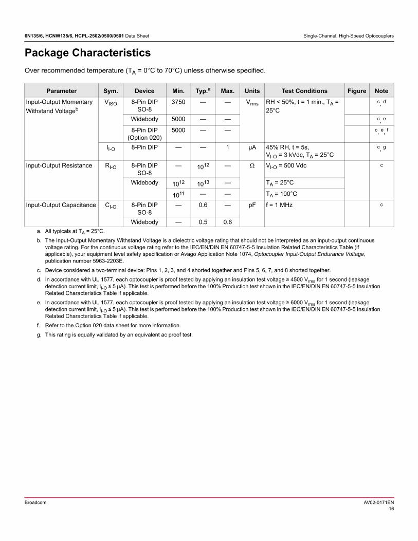
Package Characteristics
Over recommended temperature (TA = 0°C to 70°C) unless otherwise specified.
Parameter Sym. Device Min. Typ.a
a. All typicals at TA = 25°C.
Max. Units Test Conditions Figure Note
Input-Output Momentary
Withstand Voltageb
b. The Input-Output Momentary Withstand Voltage is a dielectric voltage rating that should not be interpreted as an input-output continuous voltage rating. For the continuous voltage rating refer to the IEC/EN/DIN EN 60747-5-5 Insulation Related Characteristics Table (if applicable), your equipment level safety specification or Avago Application Note 1074, Optocoupler Input-Output Endurance Voltage, publication number 5963-2203E.
VISO 8-Pin DIP SO-8
3750 — — Vrms RH < 50%, t = 1 min., TA =
25°C
c, d
c. Device considered a two-terminal device: Pins 1, 2, 3, and 4 shorted together and Pins 5, 6, 7, and 8 shorted together.
d. In accordance with UL 1577, each optocoupler is proof tested by applying an insulation test voltage ≥ 4500 Vrms for 1 second (leakage detection current limit, II-O ≤ 5 µA). This test is performed before the 100% Production test shown in the IEC/EN/DIN EN 60747-5-5 Insulation Related Characteristics Table if applicable.
Widebody 5000 — — c, e
e. In accordance with UL 1577, each optocoupler is proof tested by applying an insulation test voltage ≥ 6000 Vrms for 1 second (leakage detection current limit, II-O ≤ 5 µA). This test is performed before the 100% Production test shown in the IEC/EN/DIN EN 60747-5-5 Insulation Related Characteristics Table if applicable.
8-Pin DIP (Option 020)
5000 — — c, e, f
f. Refer to the Option 020 data sheet for more information.
II-O 8-Pin DIP — — 1 µA 45% RH, t = 5s, VI-O = 3 kVdc, TA = 25°C
c, g
g. This rating is equally validated by an equivalent ac proof test.
Input-Output Resistance RI-O 8-Pin DIP SO-8
— 1012 — VI-O = 500 Vdc c
Widebody 1012 1013 — TA = 25°C
1011 — — TA = 100°C
Input-Output Capacitance CI-O 8-Pin DIP SO-8
— 0.6 — pF f = 1 MHz c
Widebody — 0.5 0.6
Broadcom AV02-0171EN16
6N135/6, HCNW135/6, HCPL-2502/0500/0501 Data Sheet Single-Channel, High-Speed Optocouplers
Figure 1: DC and Pulsed Transfer Characteristics
Figure 2: Current Transfer Ratio vs. Input Current
Figure 3: Input Current vs. Forward Voltage
10
5
00 10 20
VO - OUTPUT VOLTAGE - V
40 mA
35 mA
30 mA
25 mA
20 mA
15 mA
10 mA
I = 5 mAF
T = 25 CV = 5.0 VACC
I O Ð
OU
TPU
T C
UR
REN
T -
mA
8 PIN DIP, SO-8
12
8
00 10 20
VO - OUTPUT VOLTAGE - V
40 mA
35 mA30 mA25 mA
20 mA
15 mA
10 mA
I = 5 mAFI O Ð
OU
TPU
T C
UR
REN
T Ð
mA
4
16T = 25 CV = 5.0 VACC
WIDEBODY
NORMALIZEDI = 16 mAV = 0.4 VV = 5 VT = 25 C
FOCCA
6N135, HCPL-05001.5
1.0
0.5
0.10 1 10 100N
OR
MA
LIZE
D C
UR
REN
T TR
AN
SFER
RA
TIO
IF - INPUT CURRENT - mA
6N136, HCPL-2502 HCPL-0501
8 PIN DIP, SO-8
FOCCA0
0 1 10 100NO
RM
ALI
ZED
CU
RR
ENT
TRA
NSF
ER R
ATI
O
IF - INPUT CURRENT - mA
1.5
0.5
1.0
NORMALIZEDI = 16 mAV = 0.4 VV = 4.5 VT = 25 C
HCNW135/6
WIDEBODY
VF - FORWARD VOLTAGE - VOLTS
100
10
0.1
0.01
1.1 1.2 1.3 1.4
I F -
FO
RW
AR
D C
UR
REN
T -
mA
1.61.5
1.0
0.001
1000
IF
VF+
T = 25 CA
-
8 PIN DIP, SO-8
VF - FORWARD VOLTAGE - VOLTS
1000
100
10
1.0
0.1
0.01
0.0011.2 1.3 1.4 1.5
T = 25 CA
I F -
FO
RW
AR
D C
UR
REN
T -
mA
IF
VF+
-
1.81.71.6
WIDEBODY
Broadcom AV02-0171EN17
6N135/6, HCNW135/6, HCPL-2502/0500/0501 Data Sheet Single-Channel, High-Speed Optocouplers
Figure 4: Current Transfer Ratio vs. Temperature
Figure 5: Propagation Delay vs. Temperature
Figure 6: Propagation Delay Time vs. Load Resistance
6N135/6, HCNW135/6, HCPL-2502/0500/0501 Data Sheet Single-Channel, High-Speed Optocouplers
Figure 7: Logic High Output Current vs. Temperature
Figure 8: Small-Signal Current Transfer Ratio vs. Quiescent Input Current
Figure 9: Thermal Derating Curve, Dependence of Safety Limiting Value with Case Temperature per IEC/EN/DIN EN 60747-5-5
TA - TEMPERATURE - C
I = 0V = V = 5.0 VCCOF
-50 -25 0 +25 +50 +75 +100
10+4
10-2
10-1
100
10+1
10+2
10+3
I OH
- L
OG
IC H
IGH
OU
TPU
T C
UR
REN
T -
nA
-75
8 PIN DIP, SO-8
I OH
- L
OG
IC H
IGH
OU
TPU
T C
UR
REN
T -
nA
TA - TEMPERATURE - C
-60 -20 0 20 40 100100
10+1
10+2
10+3
-40 8060
I = 0V = V = 15 VCCOF
WIDEBODY
I FI O-
SM
ALL
SIG
NA
L C
UR
REN
T TR
AN
SFER
RA
TIO
0
0.10
0.20
0.30
0
IF - QUIESCENT INPUT CURRENT - mA
25164 8 12 20
TA = 25 C, RL = 100 , VCC = 5 V
8 PIN DIP, SO-8
0
0.10
0.30
0 4 8 12 16 25
0.20
0.40
20
0.50
I FI O-
SMA
LL S
IGN
AL
CU
RR
ENT
TRA
NSF
ER R
ATI
O
IF - QUIESCENT INPUT CURRENT - mA
TA = 25 C, RL = 100 , VCC = 5 V
WIDEBODY
OU
TPU
T PO
WER
- P
S, IN
PUT
CU
RR
ENT
- I S
00
TS - CASE TEMPERATURE - C
175
1000
50
400
12525 75 100 150
600
800
200
100
300
500
700
900PS (mW)IS (mA)
HCNW135/6
OU
TPU
T PO
WER
- P
S, IN
PUT
CU
RR
ENT
- I S
00
TS - CASE TEMPERATURE - C
20050
400
12525 75 100 150 175
600
800
200
100
300
500
700PS (mW)IS (mA) For 8-PIN DIPIS (mA) For S0-8
8-PIN DIP/S0-8
Broadcom AV02-0171EN19
6N135/6, HCNW135/6, HCPL-2502/0500/0501 Data Sheet Single-Channel, High-Speed Optocouplers
Figure 10: Frequency Response
Figure 11: Switching Test Current
Figure 12: Test Circuit for Transient Immunity and Typical Waveforms
0.1 1.0 10 100-20
-15
-10
-5
0
+5TA = 25 C
f - FREQUENCY - MHz
NO
RM
ALI
ZED
RES
PON
SE -
dB
6N135/6, HCPL-0500/1, HCPL-2502
7
1
2
3
4 5
6
8
+12 V
0.1 μF
VFF
47 μF
51
2.1 K
100
1 K
1N4150 22
RT
Q1
TRIM FORUNITY GAIN
1.2 K15 K
9.1 K
0.1 μF
100
Q2
Q3
470
+12 V
0.1 μF
(1 M 12 pFTEST INPUT)
p-pTYPICAL LINEARITY = ± 3% AT V = 1 VTYPICAL SNR = 50dBTYPICAL R = 375 TYPICAL V dc = 3.8 VTYPICAL I = 9 mA
IN
TO
F
1 2 3Q , Q , Q : 2N3904
VO
6N135/6, HCPL-0500/1, HCPL-2502
VO
PULSEGEN.
Z = 50t = 5 nsOr
I MONITORF
IF
0.1μF
LR
CL = 1.5 μF RM
0
tPHL tPLH
OV
IF
OLV1.5 V
+5 V1
2
3
4
8
7
6
5
1.5 V
5 V
10% DUTY CYCLE1/f < 100 μS
OV 5 V
OLVOV
0 V10% 90% 90% 10%
SWITCH AT A: I = 0 mAF
SWITCH AT B: I = 16 mAF
CMV
t r t f7
1
2
3
4 5
6
8
VO
0.1 μF
LR
+5 V
PULSE GEN.
VCM+ -
V
IF
A
B
FF
Broadcom AV02-0171EN20
Broadcom, the pulse logo, Connecting everything, Avago Technologies, Avago, and the A logo are among the trademarks of Broadcom and/or its affiliates in the United States, certain other countries, and/or the EU.
The term “Broadcom” refers to Broadcom Inc. and/or its subsidiaries. For more information, please visit www.broadcom.com.
Broadcom reserves the right to make changes without further notice to any products or data herein to improve reliability, function, or design. Information furnished by Broadcom is believed to be accurate and reliable. However, Broadcom does not assume any liability arising out of the application or use of this information, nor the application or use of any product or circuit described herein, neither does it convey any license under its patent rights nor the rights of others.