398
7 Series FPGAs Integrated Block for PCI Express v3.0 LogiCORE IP Product Guide Vivado Design Suite PG054 November 19, 2014
| Date post: | 30-Dec-2016 |
| Category: |
Documents |
| Upload: | hoangtuong |
| View: | 294 times |
| Download: | 5 times |
7 Series FPGAs Integrated Block for PCI Express v3.0 LogiCORE IP Product Guide
Vivado Design Suite
PG054 November 19, 2014
7 Series Integrated Block for PCIe v3.0 www.xilinx.com 2PG054 November 19, 2014
Table of ContentsIP Facts
Chapter 1: OverviewFeature Summary. . . . . . . . . . . . . . . . . . . . . . . . . . . . . . . . . . . . . . . . . . . . . . . . . . . . . . . . . . . . . . . . . . 5Applications . . . . . . . . . . . . . . . . . . . . . . . . . . . . . . . . . . . . . . . . . . . . . . . . . . . . . . . . . . . . . . . . . . . . . . 6Licensing and Ordering Information . . . . . . . . . . . . . . . . . . . . . . . . . . . . . . . . . . . . . . . . . . . . . . . . . . . 6
Chapter 2: Product SpecificationStandards Compliance . . . . . . . . . . . . . . . . . . . . . . . . . . . . . . . . . . . . . . . . . . . . . . . . . . . . . . . . . . . . . . 8Resource Utilization. . . . . . . . . . . . . . . . . . . . . . . . . . . . . . . . . . . . . . . . . . . . . . . . . . . . . . . . . . . . . . . . 9Minimum Device Requirements . . . . . . . . . . . . . . . . . . . . . . . . . . . . . . . . . . . . . . . . . . . . . . . . . . . . . 10Available Integrated Blocks for PCIe. . . . . . . . . . . . . . . . . . . . . . . . . . . . . . . . . . . . . . . . . . . . . . . . . . 11Core Interfaces . . . . . . . . . . . . . . . . . . . . . . . . . . . . . . . . . . . . . . . . . . . . . . . . . . . . . . . . . . . . . . . . . . . 12Transaction Interface. . . . . . . . . . . . . . . . . . . . . . . . . . . . . . . . . . . . . . . . . . . . . . . . . . . . . . . . . . . . . . 15PCI Configuration Space . . . . . . . . . . . . . . . . . . . . . . . . . . . . . . . . . . . . . . . . . . . . . . . . . . . . . . . . . . . 39
Chapter 3: Designing with the CoreGeneral Design Guidelines . . . . . . . . . . . . . . . . . . . . . . . . . . . . . . . . . . . . . . . . . . . . . . . . . . . . . . . . . 45Tandem Configuration. . . . . . . . . . . . . . . . . . . . . . . . . . . . . . . . . . . . . . . . . . . . . . . . . . . . . . . . . . . . 153Clocking. . . . . . . . . . . . . . . . . . . . . . . . . . . . . . . . . . . . . . . . . . . . . . . . . . . . . . . . . . . . . . . . . . . . . . . . 181Resets . . . . . . . . . . . . . . . . . . . . . . . . . . . . . . . . . . . . . . . . . . . . . . . . . . . . . . . . . . . . . . . . . . . . . . . . . 184Protocol Layers. . . . . . . . . . . . . . . . . . . . . . . . . . . . . . . . . . . . . . . . . . . . . . . . . . . . . . . . . . . . . . . . . . 185Shared Logic . . . . . . . . . . . . . . . . . . . . . . . . . . . . . . . . . . . . . . . . . . . . . . . . . . . . . . . . . . . . . . . . . . . . 187FPGA Configuration . . . . . . . . . . . . . . . . . . . . . . . . . . . . . . . . . . . . . . . . . . . . . . . . . . . . . . . . . . . . . . 194
Chapter 4: Design Flow StepsCustomizing and Generating the Core . . . . . . . . . . . . . . . . . . . . . . . . . . . . . . . . . . . . . . . . . . . . . . . 203Constraining the Core . . . . . . . . . . . . . . . . . . . . . . . . . . . . . . . . . . . . . . . . . . . . . . . . . . . . . . . . . . . . 239Simulation . . . . . . . . . . . . . . . . . . . . . . . . . . . . . . . . . . . . . . . . . . . . . . . . . . . . . . . . . . . . . . . . . . . . . 254Synthesis and Implementation . . . . . . . . . . . . . . . . . . . . . . . . . . . . . . . . . . . . . . . . . . . . . . . . . . . . . 257
Chapter 5: Detailed Example DesignsIntegrated Block Endpoint Configuration Overview . . . . . . . . . . . . . . . . . . . . . . . . . . . . . . . . . . . . 258
Send Feedback

7 Series Integrated Block for PCIe v3.0 www.xilinx.com 3PG054 November 19, 2014
Programmed Input/Output: Endpoint Example Design . . . . . . . . . . . . . . . . . . . . . . . . . . . . . . . . . 261Configurator Example Design . . . . . . . . . . . . . . . . . . . . . . . . . . . . . . . . . . . . . . . . . . . . . . . . . . . . . . 275Generating the Core. . . . . . . . . . . . . . . . . . . . . . . . . . . . . . . . . . . . . . . . . . . . . . . . . . . . . . . . . . . . . . 281Simulating the Example Design. . . . . . . . . . . . . . . . . . . . . . . . . . . . . . . . . . . . . . . . . . . . . . . . . . . . . 284Synthesizing and Implementing the Example Design . . . . . . . . . . . . . . . . . . . . . . . . . . . . . . . . . . . 285Directory and File Contents. . . . . . . . . . . . . . . . . . . . . . . . . . . . . . . . . . . . . . . . . . . . . . . . . . . . . . . . 286
Chapter 6: Test BenchesRoot Port Model Test Bench for Endpoint . . . . . . . . . . . . . . . . . . . . . . . . . . . . . . . . . . . . . . . . . . . . 296Endpoint Model Test Bench for Root Port . . . . . . . . . . . . . . . . . . . . . . . . . . . . . . . . . . . . . . . . . . . . 308
Appendix A: Migrating and UpgradingMigrating to the Vivado Design Suite. . . . . . . . . . . . . . . . . . . . . . . . . . . . . . . . . . . . . . . . . . . . . . . . 311Upgrading in the Vivado Design Suite . . . . . . . . . . . . . . . . . . . . . . . . . . . . . . . . . . . . . . . . . . . . . . . 322
Appendix B: DebuggingFinding Help on Xilinx.com . . . . . . . . . . . . . . . . . . . . . . . . . . . . . . . . . . . . . . . . . . . . . . . . . . . . . . . . 325Debug Tools . . . . . . . . . . . . . . . . . . . . . . . . . . . . . . . . . . . . . . . . . . . . . . . . . . . . . . . . . . . . . . . . . . . . 327Simulation Debug. . . . . . . . . . . . . . . . . . . . . . . . . . . . . . . . . . . . . . . . . . . . . . . . . . . . . . . . . . . . . . . . 330Hardware Debug . . . . . . . . . . . . . . . . . . . . . . . . . . . . . . . . . . . . . . . . . . . . . . . . . . . . . . . . . . . . . . . . 333
Appendix C: Managing Receive-Buffer Space for Inbound CompletionsGeneral Considerations and Concepts . . . . . . . . . . . . . . . . . . . . . . . . . . . . . . . . . . . . . . . . . . . . . . . 347Methods of Managing Completion Space . . . . . . . . . . . . . . . . . . . . . . . . . . . . . . . . . . . . . . . . . . . . 348
Appendix D: PCIE_2_1 Port DescriptionsClock and Reset Interface . . . . . . . . . . . . . . . . . . . . . . . . . . . . . . . . . . . . . . . . . . . . . . . . . . . . . . . . . 354Transaction Layer Interface. . . . . . . . . . . . . . . . . . . . . . . . . . . . . . . . . . . . . . . . . . . . . . . . . . . . . . . . 355Block RAM Interface . . . . . . . . . . . . . . . . . . . . . . . . . . . . . . . . . . . . . . . . . . . . . . . . . . . . . . . . . . . . . 359GTX Transceiver Interface . . . . . . . . . . . . . . . . . . . . . . . . . . . . . . . . . . . . . . . . . . . . . . . . . . . . . . . . . 360Configuration Management Interface . . . . . . . . . . . . . . . . . . . . . . . . . . . . . . . . . . . . . . . . . . . . . . . 367Dynamic Reconfiguration Port Interface . . . . . . . . . . . . . . . . . . . . . . . . . . . . . . . . . . . . . . . . . . . . . 392TL2 Interface Ports . . . . . . . . . . . . . . . . . . . . . . . . . . . . . . . . . . . . . . . . . . . . . . . . . . . . . . . . . . . . . . . 393
Appendix E: Additional Resources and Legal NoticesXilinx Resources . . . . . . . . . . . . . . . . . . . . . . . . . . . . . . . . . . . . . . . . . . . . . . . . . . . . . . . . . . . . . . . . . 395References . . . . . . . . . . . . . . . . . . . . . . . . . . . . . . . . . . . . . . . . . . . . . . . . . . . . . . . . . . . . . . . . . . . . . 395Revision History . . . . . . . . . . . . . . . . . . . . . . . . . . . . . . . . . . . . . . . . . . . . . . . . . . . . . . . . . . . . . . . . . 396Please Read: Important Legal Notices . . . . . . . . . . . . . . . . . . . . . . . . . . . . . . . . . . . . . . . . . . . . . . . 397
Send Feedback

7 Series Integrated Block for PCIe v3.0 www.xilinx.com 4PG054 November 19, 2014 Product Specification
IntroductionThe 7 Series FPGAs Integrated Block for PCI Express® core is a scalable, high-bandwidth, and reliable serial interconnect building block for use with Xilinx® Zynq®-7000 All Programmable SoC, and 7 series FPGA families. The 7 Series Integrated Block for PCI Express (PCIe®) solution supports 1-lane, 2-lane, 4-lane, and 8-lane Endpoint and Root Port configurations at up to 5 Gb/s (Gen2) speeds, all of which are compliant with the PCI Express Base Specification, rev. 2.1. This solution supports the AMBA® AXI4-Stream interface for the customer user interface.
With higher bandwidth per pin, low overhead, low latency, reduced signal integrity issues, and CDR architecture, the 7 Series Integrated Block for PCIe sets the industry standard for a high-performance, cost-eff icient, third-generation I/O solution.
Features• High-performance, highly flexible, scalable,
and reliable, general-purpose I/O core
• Incorporates Xilinx Smart-IP technology to guarantee critical timing
• Uses GTXE2 or GTPE2 transceivers for 7 series FPGA families
° 2.5 GT/s and 5.0 GT/s line speeds
° Supports 1-lane, 2-lane, 4-lane, and 8-lane operation
° Elastic buffers and clock compensation
° Automatic clock data recovery
• Supports Endpoint and Root Port configurations
• 8B/10B encode and decode• Supports Lane Reversal and Lane Polarity
Inversion per PCI Express specif ication requirements
• Standardized user interface
• Compliant with PCI/PCI Express power management functions, and transaction ordering rules
• Supports a maximum transaction payload of up to 1024 bytes
• Supports Multi-Vector MSI for up to 32 vectors and MSI-X
• Up-configure capability enables application driven bandwidth scalability
IP Facts
LogiCORE IP Facts Table
Core SpecificsSupported Device Family(1)
Zynq-7000, Virtex®-7, Kintex®-7, Artix®-7
Supported User Interfaces AXI4-Stream
Resources See Table 2-2.
Provided with Core
Design Files Verilog/VHDL(2) RTL Sourceand Simulation Models
Example Design Verilog, VHDL
Test Bench Verilog, VHDL
Constraints File XDC
Simulation Model Verilog, VHDL
Supported S/W Driver N/A
Tested Design Flows(3)
Design EntryVivado® Design Suite
Vivado
Simulation For a list of supported simulators, see theXilinx Design Tools: Release Notes Guide
Synthesis Vivado Synthesis
SupportProvided by Xilinx @ www.xilinx.com/support
Notes: 1. For a complete listing of supported devices, see the Vivado
IP catalog.2. RTL source for the GTX wrapper is Verilog only. VHDL projects
require mixed language mode simulators. 3. For the supported versions of the tools, see the
Xilinx Design Tools: Release Notes Guide.
Send Feedback
7 Series Integrated Block for PCIe v3.0 www.xilinx.com 5PG054 November 19, 2014
Chapter 1
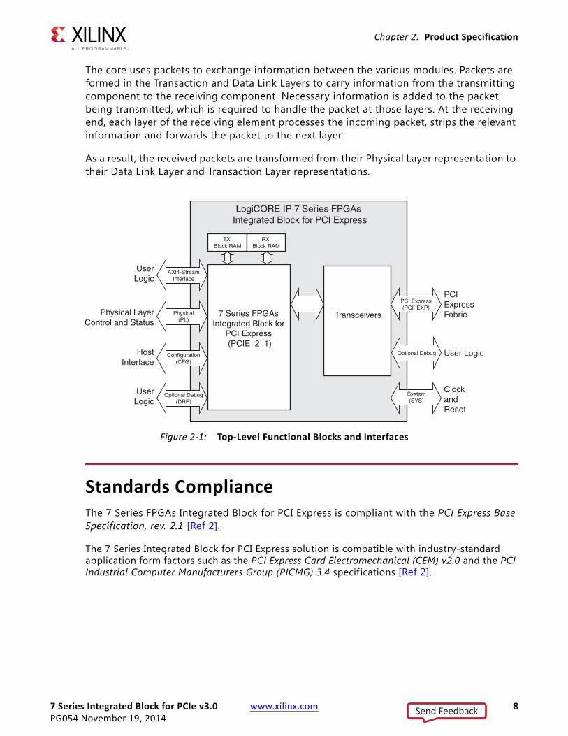
OverviewXilinx® 7 series FPGAs include three unified FPGA families that are all designed for lowest power to enable a common design to scale across families for optimal power, performance, and cost. The Artix®-7 family is optimized for lowest cost and absolute power for the highest volume applications. The Virtex®-7 family is optimized for highest system performance and capacity. The Kintex®-7 family is an innovative class of FPGAs optimized for the best price to performance. This document describes the function and operation of the 7 Series FPGAs Integrated Block for PCI Express®, including how to design, customize, and implement it.
The 7 Series FPGAs Integrated Block for PCI Express core is a reliable, high-bandwidth, scalable serial interconnect building block. The core instantiates the 7 Series Integrated Block for PCI Express found in the 7 series FPGAs, and supports both Verilog and VHDL. This core simplif ies the design process and reduces time to market. It is configurable for Endpoint and Root Port applications. This solution can be used in communication, multimedia, server and mobile platforms and enables applications such as high-end medical imaging, graphics intensive video games, DVD quality streaming video on the desktop, and 10 Gigabit Ethernet interface cards.
Although the core is a fully verif ied solution, the challenge associated with implementing a complete design varies depending on the configuration and functionality of the application.
RECOMMENDED: For the best results, previous experience building high-performance, pipelined FPGA designs using Xilinx implementation software and constraints files is recommended.
Feature SummaryThe 7 Series Integrated Block for PCIe follows the PCI Express Base Specification, rev. 2.1 [Ref 2] layering model, which consists of the Physical, Data Link, and Transaction Layers. The protocol uses packets to exchange information between layers. Packets are formed in the Transaction and Data Link Layers to carry information from the transmitting component to the receiving component. Necessary information is added to the packet being transmitted, which is required to handle the packet at specif ic layers.
Send Feedback

7 Series Integrated Block for PCIe v3.0 www.xilinx.com 6PG054 November 19, 2014
Chapter 1: Overview
The functions of the protocol layers include:
• Generating and processing of TLPs
• Flow-control management
• Initialization and power management functions
• Data protection
• Error checking and retry functions
• Physical link interface initialization
• Maintenance and status tracking
• Serialization, deserialization, and other circuitry for interface operation
ApplicationsThe Xilinx 7 series FPGAs Integrated Block for PCI Express architecture enables a broad range of computing and communications target applications, emphasizing performance, cost, scalability, feature extensibility and mission-critical reliability. Typical applications include:
• Data communications networks
• Telecommunications networks
• Broadband wired and wireless applications
• Cross-connects
• Network interface cards
• Chip-to-chip and backplane interconnect
• Crossbar switches
• Wireless base stations
Licensing and Ordering InformationThis Xilinx LogiCORE IP module is provided at no additional cost with the Xilinx Vivado® Design Suite under the terms of the Xilinx End User License. Information about this and other Xilinx LogiCORE IP modules is available at the Xilinx Intellectual Property page. For information about pricing and availability of other Xilinx LogiCORE IP modules and tools, contact your local Xilinx sales representative.
For more information, visit the 7 Series FPGAs Integrated Block for PCI Express product page.
Send Feedback

7 Series Integrated Block for PCIe v3.0 www.xilinx.com 7PG054 November 19, 2014
Chapter 2
Product SpecificationThe 7 Series FPGAs Integrated Block for PCI Express® contains full support for 2.5 Gb/s and 5.0 Gb/s PCI Express Endpoint and Root Port configurations. For 8.0 Gb/s (Gen3) support, see Virtex-7 FPGA Gen3 Integrated Block for PCI Express Product Guide (PG023) [Ref 4] for device support and information on the Virtex®-7 FPGA Gen3 Integrated Block for PCI Express.
Table 2-1 defines the Integrated Block for PCIe® solutions.
The Xilinx 7 Series FPGAs Integrated Block for PCI Express core internally instantiates the 7 Series FPGAs Integrated Block for PCI Express (PCIE_2_1). The integrated block follows the PCI Express Base Specif ication layering model, which consists of the Physical, Data Link, and Transaction layers. The integrated block is compliant with the PCI Express Base Specification, rev. 2.1 [Ref 2].
Figure 2-1 illustrates these interfaces to the 7 Series FPGAs Integrated Block for PCI Express core:
• System (SYS) interface
• PCI Express (PCI_EXP) interface
• Configuration (CFG) interface
• Transaction interface (AXI4-Stream)
• Physical Layer Control and Status (PL) interface
Table 2-1: Product Overview
Product Name User Interface Width Supported Lane Widths
1-lane at 2.5 Gb/s, 5.0 Gb/s 64 x1
2-lane at 2.5 Gb/s, 5.0 Gb/s 64 x1, x2(1)
4-lane at 2.5 Gb/s, 5.0 Gb/s 64, 128 x1, x2, x4(1),(2)
8-lane at 2.5 Gb/s, 5.0 Gb/s 64, 128 x1, x2, x4, x8(1),(3)
Notes: 1. See Link Training: 2-Lane, 4-Lane, and 8-Lane Components, page 140 for additional information. 2. The x4 at 2.5 Gb/s option in the Vivado® IP catalog provides only the 64-bit width interface.3. x8 at 5.0 Gb/s only available in the 128-bit width.
Send Feedback
7 Series Integrated Block for PCIe v3.0 www.xilinx.com 8PG054 November 19, 2014
Chapter 2: Product Specification
The core uses packets to exchange information between the various modules. Packets are formed in the Transaction and Data Link Layers to carry information from the transmitting component to the receiving component. Necessary information is added to the packet being transmitted, which is required to handle the packet at those layers. At the receiving end, each layer of the receiving element processes the incoming packet, strips the relevant information and forwards the packet to the next layer.
As a result, the received packets are transformed from their Physical Layer representation to their Data Link Layer and Transaction Layer representations.
Standards ComplianceThe 7 Series FPGAs Integrated Block for PCI Express is compliant with the PCI Express Base Specification, rev. 2.1 [Ref 2].
The 7 Series Integrated Block for PCI Express solution is compatible with industry-standard application form factors such as the PCI Express Card Electromechanical (CEM) v2.0 and the PCI Industrial Computer Manufacturers Group (PICMG) 3.4 specif ications [Ref 2].
X-Ref Target - Figure 2-1
Figure 2-1: Top-Level Functional Blocks and Interfaces
LogiCORE IP 7 Series FPGAs Integrated Block for PCI Express
7 Series FPGAs Integrated Block for
PCI Express (PCIE_2_1)
Transceivers
Optional Debug
System(SYS)
User Logic
PCIExpressFabric
ClockandReset
PCI Express(PCI_EXP)
UserLogic
Physical LayerControl and Status
HostInterface
AXI4-StreamInterface
UserLogic
Optional Debug(DRP)
Physical(PL)
Configuration(CFG)
TX Block RAM
RX Block RAM
Send Feedback
7 Series Integrated Block for PCIe v3.0 www.xilinx.com 9PG054 November 19, 2014
Chapter 2: Product Specification
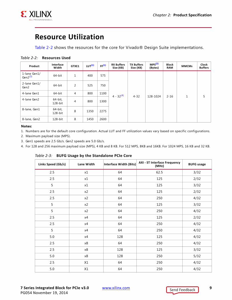
Resource UtilizationTable 2-2 shows the resources for the core for Vivado® Design Suite implementations.
Table 2-2: Resources Used
Product InterfaceWidth GTXE1 LUT(1) FF(1) RX Buffers
Size (KB)TX BuffersSize (KB)
MPS(2)
(Bytes)BlockRAM MMCMs Clock
Buffers
1-lane Gen1/Gen2(3) 64-bit 1 400 575
4 - 32(4) 4-32 128-1024 2-16 1 5
2-lane Gen1/Gen2 64-bit 2 525 750
4-lane Gen1 64-bit 4 800 1100
4-lane Gen2 64-bit, 128-bit 4 800 1300
8-lane, Gen1 64-bit, 128-bit 8 1350 2275
8-lane, Gen2 128-bit 8 1450 2600
Notes: 1. Numbers are for the default core configuration. Actual LUT and FF utilization values vary based on specific configurations.2. Maximum payload size (MPS). 3. Gen1 speeds are 2.5 Gb/s. Gen2 speeds are 5.0 Gb/s.4. For 128 and 256 maximum payload size (MPS), 4 KB and 8 KB. For 512 MPS, 8KB and 16KB. For 1024 MPS, 16 KB and 32 KB.
Table 2-3: BUFG Usage by the Standalone PCIe Core
Links Speed (Gb/s) Lane Width Interface Width (Bits) AXI - ST Interface Frequency (MHz) BUFG usage
2.5 x1 64 62.5 3/32
2.5 x1 64 125 2/32
5 x1 64 125 3/32
2.5 x2 64 125 2/32
2.5 x2 64 250 4/32
5 x2 64 125 3/32
5 x2 64 250 4/32
2.5 x4 64 125 2/32
2.5 x4 64 250 4/32
5 x4 64 250 4/32
5.0 x4 128 125 4/32
2.5 x8 64 250 4/32
2.5 x8 128 125 3/32
5.0 x8 128 250 5/32
2.5 X1 64 250 4/32
5.0 X1 64 250 4/32
Send Feedback

7 Series Integrated Block for PCIe v3.0 www.xilinx.com 10PG054 November 19, 2014
Chapter 2: Product Specification
Minimum Device RequirementsTable 2-4 lists the minimum device requirements for 7 Series Integrated Block for PCIe configurations.
Table 2-4: Core Configurations
Zynq®-7000 Devices Virtex®-7 FPGAs Kintex®-7
FPGAsArtix®-7FPGAs(3)
ZC7015(1)
ZC7030ZC7035ZC7045ZC7100
XC7VX485T XC7V585T XC7V2000T
XC7K325TXC7K355TXC7K410TXC7K420
XC7K480T XCK7160T(2) XC7K70T(2)
XC7A15TXC7A35TXC7A50TXC7A75T
XC7A100TXC7A200T
Number of Integrated Blocks for PCIe (see Table 2-5) 1 4 3 4 1 1
Lanes
Gen1 (2.5 Gb/s) 1-4 or 1-8(5) 1–8 1–8 1–8 1–8 1–4
Gen2 (5.0 Gb/s) 1-4 or 1-8(5) 1–8 1–8 1–8 1–8 1–4
Gen3 (8.0 Gb/s)(4) — — — — — —
Speed Grade
x1–x4 Gen1 -1, -2, -3, -2L -1, -2, -3, -2L -1, -2, -3, -2L -1, -2, -2L -1, -2, -3, -2L -1, -2, -3,-2L
x8 Gen1 -1, -2, -3, -2L -1, -2, -3, -2L -1, -2, -3, -2L -1, -2, -2L -1, -2, -3, -2L NA
x1–x4 Gen2 -1, -2, -3, -2L (1V)
-1, -2, -3, -2L (1V)
-1, -2, -3, -2L (1V) -1, -2, -2L (1V) -1, -2, -3,
-2L (1V) -2, -3 (1V)
x8 Gen2 -2, -3, -2L (1V) -2, -3, -2L (1V) -2, -3, -2L (1V) -2, -2L (1V) -2, -3, -2L (1V) NA
Maximum Payload
Size MPS (Bytes)
Gen1 1024 1024 1024 1024 1024 1024
x1–x4 Gen2 -2L (1V) -2L (1V) -2L (1V) -2L (1V) -2L (1V) -2L (1V)
x8 Gen2512 (-3)(7)
256 (-2, -2L (1V))
512 (-3)256 (-2, -2L
(1V))
512 (-3)256 (-2, -2L
(1V))
512 (-3)256 (-2, -2L
(1V))
512 (-3)256 (-2, -2L
(1V))NA
Notes: 1. The Zynq-7000 ZC7015 package does not support Gen2 in -1 speedgrade.2. Kintex-7 FPGA FBG484 packages only support x1, x2, and x4 operation.
3. Artix-7 devices only support x1, x2, and x4 operation.4. The 7 Series FPGAs Integrated Block for PCI Express does not support the Gen3 operation. See Virtex-7 FPGA Gen3 Integrated Block
for PCI Express Product Guide (PG023) [Ref 4], for device support and information on the Virtex-7 FPGA Gen3 Integrated Block for PCI Express.
5. 1-4 lanes for 7030 devices, and 1-8 lanes for 7045 devices.6. Not all SSI devices-PCIe/MMCM site pairs pass timing skew checks.7. Minimum supported speed grade for the specif ied MPS value.8. Gen2 line rate is not supported for -2L (0.9V).
Send Feedback

7 Series Integrated Block for PCIe v3.0 www.xilinx.com 11PG054 November 19, 2014
Chapter 2: Product Specification
Available Integrated Blocks for PCIeTable 2-5 lists which 7 series integrated blocks are available for use in FPGAs containing multiple blocks. In some cases, not all blocks can be targeted due to lack of bonded transceiver sites adjacent to the integrated block.
\
Table 2-5: Available Integrated Blocks for PCIe
Device Selection Integrated Block for PCIe Location
Device Package X0Y0 X0Y1 X0Y2 X1Y0 X1Y1
Zynq-7000
ZC7015 All ✓
ZC7030 All ✓
ZC7035 All ✓
ZC7045 All ✓
ZC7100 All ✓
Virtex-7
XC7VX485T
FFG1157FFG1761FFG1930
✓ ✓
FFG1158FFG1927
✓ ✓ ✓ ✓
XC7V585TFFG1157 ✓ ✓
FFG1761 ✓ ✓ ✓
XC7V2000TFHG1761 ✓ ✓ ✓
FLG1925 ✓ ✓
Kintex-7
XC7K480T All ✓
XC7K420 All ✓
XC7K410T All ✓
XC7K355T All ✓
XC7K325T All ✓
XCK7160T All ✓
XC7K70T All ✓
Artix-7
XC7A100T All ✓
XC7A200T All ✓
XC7A35T All ✓
XC7A50T All ✓
XC7A75T All ✓
XC7A15T All ✓
Send Feedback
7 Series Integrated Block for PCIe v3.0 www.xilinx.com 12PG054 November 19, 2014
Chapter 2: Product Specification
See also the recommended core pinouts in Table 4-6, page 243.
Core InterfacesThe 7 Series FPGAs Integrated Block for PCI Express core includes top-level signal interfaces that have sub-groups for the receive direction, transmit direction, and signals common to both directions.
System InterfaceThe System (SYS) interface consists of the system reset signal (sys_rst_n) and the system clock signal (sys_clk), as described in Table 2-6.
Some 7 series devices do not have 3.3 V I/Os available. Therefore the appropriate level shift is required to operate with these devices that contain only 1.8 V banks.
The system reset signal is an asynchronous input. The assertion of sys_rst_n causes a hard reset of the entire core. The system reset signal is a 3.3 V signal.
The system input clock must be 100 MHz, 125 MHz, or 250 MHz, as selected in the Vivado® IP catalog clock and reference signals.
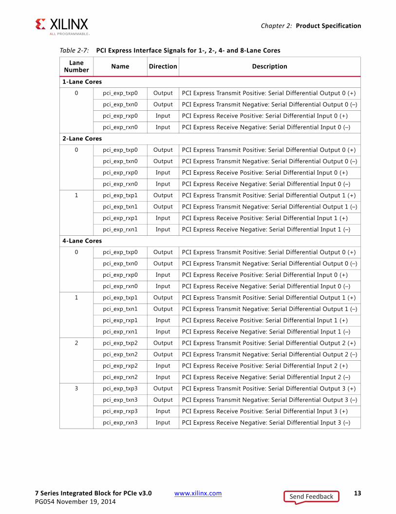
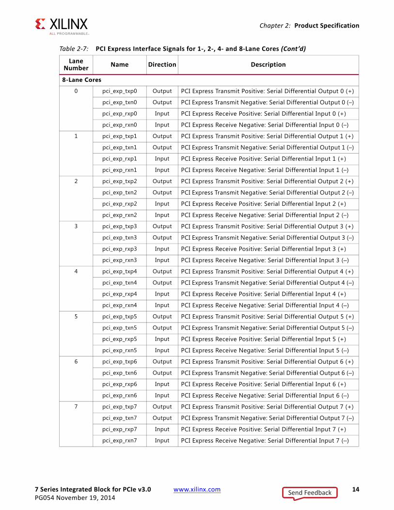
PCI Express Interface The PCI Express (PCI_EXP) interface consists of differential transmit and receive pairs organized in multiple lanes. A PCI Express lane consists of a pair of transmit differential signals (pci_exp_txp, pci_exp_txn) and a pair of receive differential signals (pci_exp_rxp, pci_exp_rxn). The 1-lane core supports only Lane 0, the 2-lane core supports lanes 0-1, the 4-lane core supports lanes 0-3, and the 8-lane core supports lanes 0-7. Transmit and receive signals of the PCI_EXP interface are defined in Table 2-7.
Table 2-6: System Interface Signals
Function Signal Name Direction Description
System Reset sys_rst_n InputAsynchronous signal. sys_rst_n must be asserted for at least 1500 ns during power on and warm reset operations.
System Clock sys_clk Input Reference clock: Selectable frequency 100 MHz, 125 MHz, or 250 MHz.
Send Feedback
7 Series Integrated Block for PCIe v3.0 www.xilinx.com 13PG054 November 19, 2014
Chapter 2: Product Specification
Table 2-7: PCI Express Interface Signals for 1-, 2-, 4- and 8-Lane Cores
Lane Number Name Direction Description
1-Lane Cores
0 pci_exp_txp0 Output PCI Express Transmit Positive: Serial Differential Output 0 (+)
pci_exp_txn0 Output PCI Express Transmit Negative: Serial Differential Output 0 (–)
pci_exp_rxp0 Input PCI Express Receive Positive: Serial Differential Input 0 (+)
pci_exp_rxn0 Input PCI Express Receive Negative: Serial Differential Input 0 (–)
2-Lane Cores
0 pci_exp_txp0 Output PCI Express Transmit Positive: Serial Differential Output 0 (+)
pci_exp_txn0 Output PCI Express Transmit Negative: Serial Differential Output 0 (–)
pci_exp_rxp0 Input PCI Express Receive Positive: Serial Differential Input 0 (+)
pci_exp_rxn0 Input PCI Express Receive Negative: Serial Differential Input 0 (–)
1 pci_exp_txp1 Output PCI Express Transmit Positive: Serial Differential Output 1 (+)
pci_exp_txn1 Output PCI Express Transmit Negative: Serial Differential Output 1 (–)
pci_exp_rxp1 Input PCI Express Receive Positive: Serial Differential Input 1 (+)
pci_exp_rxn1 Input PCI Express Receive Negative: Serial Differential Input 1 (–)
4-Lane Cores
0 pci_exp_txp0 Output PCI Express Transmit Positive: Serial Differential Output 0 (+)
pci_exp_txn0 Output PCI Express Transmit Negative: Serial Differential Output 0 (–)
pci_exp_rxp0 Input PCI Express Receive Positive: Serial Differential Input 0 (+)
pci_exp_rxn0 Input PCI Express Receive Negative: Serial Differential Input 0 (–)
1 pci_exp_txp1 Output PCI Express Transmit Positive: Serial Differential Output 1 (+)
pci_exp_txn1 Output PCI Express Transmit Negative: Serial Differential Output 1 (–)
pci_exp_rxp1 Input PCI Express Receive Positive: Serial Differential Input 1 (+)
pci_exp_rxn1 Input PCI Express Receive Negative: Serial Differential Input 1 (–)
2 pci_exp_txp2 Output PCI Express Transmit Positive: Serial Differential Output 2 (+)
pci_exp_txn2 Output PCI Express Transmit Negative: Serial Differential Output 2 (–)
pci_exp_rxp2 Input PCI Express Receive Positive: Serial Differential Input 2 (+)
pci_exp_rxn2 Input PCI Express Receive Negative: Serial Differential Input 2 (–)
3 pci_exp_txp3 Output PCI Express Transmit Positive: Serial Differential Output 3 (+)
pci_exp_txn3 Output PCI Express Transmit Negative: Serial Differential Output 3 (–)
pci_exp_rxp3 Input PCI Express Receive Positive: Serial Differential Input 3 (+)
pci_exp_rxn3 Input PCI Express Receive Negative: Serial Differential Input 3 (–)
Send Feedback
7 Series Integrated Block for PCIe v3.0 www.xilinx.com 14PG054 November 19, 2014
Chapter 2: Product Specification
8-Lane Cores
0 pci_exp_txp0 Output PCI Express Transmit Positive: Serial Differential Output 0 (+)
pci_exp_txn0 Output PCI Express Transmit Negative: Serial Differential Output 0 (–)
pci_exp_rxp0 Input PCI Express Receive Positive: Serial Differential Input 0 (+)
pci_exp_rxn0 Input PCI Express Receive Negative: Serial Differential Input 0 (–)
1 pci_exp_txp1 Output PCI Express Transmit Positive: Serial Differential Output 1 (+)
pci_exp_txn1 Output PCI Express Transmit Negative: Serial Differential Output 1 (–)
pci_exp_rxp1 Input PCI Express Receive Positive: Serial Differential Input 1 (+)
pci_exp_rxn1 Input PCI Express Receive Negative: Serial Differential Input 1 (–)
2 pci_exp_txp2 Output PCI Express Transmit Positive: Serial Differential Output 2 (+)
pci_exp_txn2 Output PCI Express Transmit Negative: Serial Differential Output 2 (–)
pci_exp_rxp2 Input PCI Express Receive Positive: Serial Differential Input 2 (+)
pci_exp_rxn2 Input PCI Express Receive Negative: Serial Differential Input 2 (–)
3 pci_exp_txp3 Output PCI Express Transmit Positive: Serial Differential Output 3 (+)
pci_exp_txn3 Output PCI Express Transmit Negative: Serial Differential Output 3 (–)
pci_exp_rxp3 Input PCI Express Receive Positive: Serial Differential Input 3 (+)
pci_exp_rxn3 Input PCI Express Receive Negative: Serial Differential Input 3 (–)
4 pci_exp_txp4 Output PCI Express Transmit Positive: Serial Differential Output 4 (+)
pci_exp_txn4 Output PCI Express Transmit Negative: Serial Differential Output 4 (–)
pci_exp_rxp4 Input PCI Express Receive Positive: Serial Differential Input 4 (+)
pci_exp_rxn4 Input PCI Express Receive Negative: Serial Differential Input 4 (–)
5 pci_exp_txp5 Output PCI Express Transmit Positive: Serial Differential Output 5 (+)
pci_exp_txn5 Output PCI Express Transmit Negative: Serial Differential Output 5 (–)
pci_exp_rxp5 Input PCI Express Receive Positive: Serial Differential Input 5 (+)
pci_exp_rxn5 Input PCI Express Receive Negative: Serial Differential Input 5 (–)
6 pci_exp_txp6 Output PCI Express Transmit Positive: Serial Differential Output 6 (+)
pci_exp_txn6 Output PCI Express Transmit Negative: Serial Differential Output 6 (–)
pci_exp_rxp6 Input PCI Express Receive Positive: Serial Differential Input 6 (+)
pci_exp_rxn6 Input PCI Express Receive Negative: Serial Differential Input 6 (–)
7 pci_exp_txp7 Output PCI Express Transmit Positive: Serial Differential Output 7 (+)
pci_exp_txn7 Output PCI Express Transmit Negative: Serial Differential Output 7 (–)
pci_exp_rxp7 Input PCI Express Receive Positive: Serial Differential Input 7 (+)
pci_exp_rxn7 Input PCI Express Receive Negative: Serial Differential Input 7 (–)
Table 2-7: PCI Express Interface Signals for 1-, 2-, 4- and 8-Lane Cores (Cont’d)
Lane Number Name Direction Description
Send Feedback

7 Series Integrated Block for PCIe v3.0 www.xilinx.com 15PG054 November 19, 2014
Chapter 2: Product Specification
For more information about PCI Express clocking and reset, see PCI Express Clocking and PCI Express Reset in the “Use Model” chapter of the 7 Series FPGAs GTX/GTH Transceivers User Guide (UG476) [Ref 12].
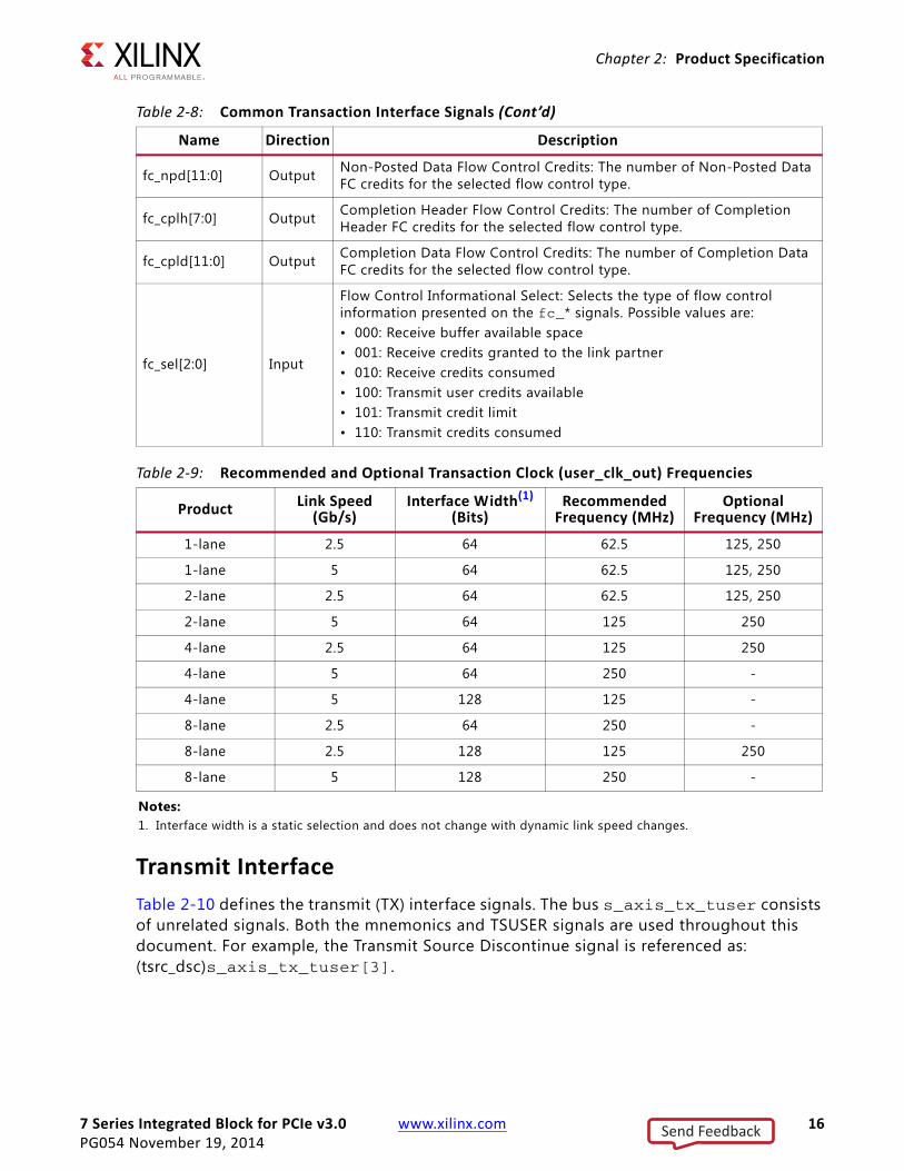
Transaction InterfaceThe transaction interface provides a mechanism for the user design to generate and consume TLPs. The signal names and signal descriptions for this interface are shown in Table 2-8, Table 2-10, and Table 2-11.
Common InterfaceTable 2-8 describes the common interface signals.
Table 2-8: Common Transaction Interface Signals
Name Direction Description
user_clk_out Output
Transaction Clock: Transaction, Configuration, and Physical Layer Control and Status Interface operations are referenced to and synchronous with the rising edge of this clock. This signal is active after power-on, and sys_rst_n has no effect on it. This signal is guaranteed to be stable at the selected operating frequency only after user_reset_out is deasserted. The user_clk_out clock output is a f ixed frequency configured in the CORE Generator tool. This signal does not change frequencies in case of link recovery or training down.See Table 2-9 for recommended and optional frequencies.
user_reset_out Output
Transaction Reset: User logic interacting with the Transaction and Configuration interfaces must use user_reset_out to return to its quiescent state. This signal is deasserted synchronously with respect to user_clk_out, and is deasserted and asserted asynchronously with sys_rst_n assertion. This signal is asserted for core in-band reset events such as Hot Reset or Link Disable.
user_lnk_up Output
Transaction Link Up: Transaction link-up is asserted when the core and the connected upstream link partner port are ready and able to exchange data packets. Transaction link-up is deasserted when the core and link partner are attempting to establish communication, or when communication with the link partner is lost due to errors on the transmission channel. This signal is also deasserted when the core is driven to Hot Reset or Link Disable state by the link partner, and all TLPs stored in the core are lost. This signal is not deasserted while in the Recovery state, but is deasserted if Recovery fails.
fc_ph[7:0] Output Posted Header Flow Control Credits: The number of Posted Header FC credits for the selected flow control type.
fc_pd[11:0] Output Posted Data Flow Control Credits: The number of Posted Data FC credits for the selected flow control type.
fc_nph[7:0] Output Non-Posted Header Flow Control Credits: The number of Non-Posted Header FC credits for the selected flow control type.
Send Feedback
7 Series Integrated Block for PCIe v3.0 www.xilinx.com 16PG054 November 19, 2014
Chapter 2: Product Specification
Transmit InterfaceTable 2-10 defines the transmit (TX) interface signals. The bus s_axis_tx_tuser consists of unrelated signals. Both the mnemonics and TSUSER signals are used throughout this document. For example, the Transmit Source Discontinue signal is referenced as: (tsrc_dsc)s_axis_tx_tuser[3].
fc_npd[11:0] Output Non-Posted Data Flow Control Credits: The number of Non-Posted Data FC credits for the selected flow control type.
fc_cplh[7:0] Output Completion Header Flow Control Credits: The number of Completion Header FC credits for the selected flow control type.
fc_cpld[11:0] Output Completion Data Flow Control Credits: The number of Completion Data FC credits for the selected flow control type.
fc_sel[2:0] Input
Flow Control Informational Select: Selects the type of flow control information presented on the fc_* signals. Possible values are:• 000: Receive buffer available space• 001: Receive credits granted to the link partner• 010: Receive credits consumed• 100: Transmit user credits available• 101: Transmit credit limit• 110: Transmit credits consumed
Table 2-9: Recommended and Optional Transaction Clock (user_clk_out) Frequencies
Product Link Speed (Gb/s)
Interface Width(1) (Bits)
Recommended Frequency (MHz)
Optional Frequency (MHz)
1-lane 2.5 64 62.5 125, 250
1-lane 5 64 62.5 125, 250
2-lane 2.5 64 62.5 125, 250
2-lane 5 64 125 250
4-lane 2.5 64 125 250
4-lane 5 64 250 -
4-lane 5 128 125 -
8-lane 2.5 64 250 -
8-lane 2.5 128 125 250
8-lane 5 128 250 -
Notes: 1. Interface width is a static selection and does not change with dynamic link speed changes.
Table 2-8: Common Transaction Interface Signals (Cont’d)
Name Direction Description
Send Feedback

7 Series Integrated Block for PCIe v3.0 www.xilinx.com 17PG054 November 19, 2014
Chapter 2: Product Specification
Table 2-10: Transmit Interface Signals
Name Mnemonic Direction Description
s_axis_tx_tlast Input Transmit End-of-Frame (EOF): Signals the end of a packet. Valid only along with assertion of s_axis_tx_tvalid.
s_axis_tx_tdata[W-1:0] Input Transmit Data: Packet data to be transmitted.
s_axis_tx_tkeep[7:0] (64-bit interface)
s_axis_tx_tkeep[15:0] (128-bit interface)
Input Transmit Data Strobe: Determines which data bytes are valid on s_axis_tx_tdata[W-1:0] during a given beat (s_axis_tx_tvalid and s_axis_tx_tready both asserted).• Bit 0 corresponds to the least significant byte on s_axis_tx_tdata.
• Bit 7 (64-bit) and bit 15 (128-bit) correspond to the most significant byte.
For example:• s_axis_tx_tkeep[0] ==1b, s_axis_tx_tdata[7:0] is valid• s_axis_tx_tkeep[7] ==0b, s_axis_tx_tdata[63:56] is not validWhen s_axis_tx_tlast is not asserted, the only valid values are 0xFF (64-bit) or 0xFFFF (128-bit). When s_axis_tx_tlast is asserted, valid values are:• 64-bit: only 0x0F and 0xFF are valid.• 128-bit: 0x000F, 0x00FF, 0x0FFF, and 0xFFFF are valid.
s_axis_tx_tvalid Input Transmit Source Ready: Indicates that the user application is presenting valid data on s_axis_tx_tdata.
s_axis_tx_tready Output Transmit Destination Ready: Indicates that the core is ready to accept data on s_axis_tx_tdata. The simultaneous assertion of s_axis_tx_tvalid and s_axis_tx_tready marks the successful transfer of one data beat on s_axis_tx_tdata.
s_axis_tx_tuser[3] t_src_dsc Input Transmit Source Discontinue: Can be asserted any time starting on the f irst cycle after start-of-frame (SOF). Assert s_axis_tx_tlast simultaneously with (tx_src_dsc)s_axis_tx_tuser[3].
tx_buf_av[5:0] Output Transmit Buffers Available: Indicates the number of free transmit buffers available in the core. Each free transmit buffer can accommodate one TLP up to the supported maximum payload size (MPS). The maximum number of transmit buffers is determined by the supported MPS and block RAM configuration selected. (See Core Buffering and Flow Control, page 92.)
Product Data Bus Width (W)
1-lane (2.5 Gb/s and 5.0 Gb/s) 64
2-lane (2.5 Gb/s and 5.0 Gb/s) 64
4-lane (2.5 Gb/s and 5.0 Gb/s) 64 or 128
8-lane (2.5 Gb/s and 5.0 Gb/s) 64 or 128
Send Feedback

7 Series Integrated Block for PCIe v3.0 www.xilinx.com 18PG054 November 19, 2014
Chapter 2: Product Specification
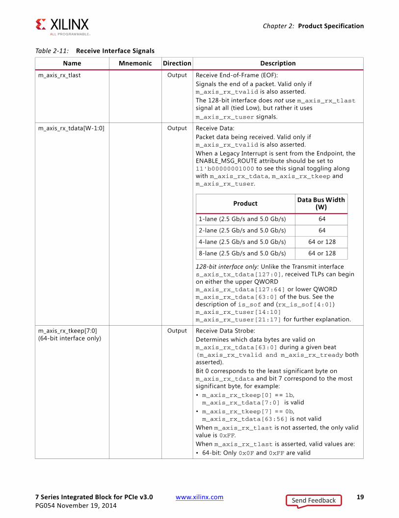
Receive InterfaceTable 2-11 defines the receive (RX) interface signals. The bus m_axis_tx_tuser consists of unrelated signals. Mnemonics for these signals are used throughout this document in place of the TUSER signal names.
tx_err_drop Output Transmit Error Drop: Indicates that the core discarded a packet because of a length violation or, when streaming, data was not presented on consecutive clock cycles.
s_axis_tx_tuser[2] tx_str Input Transmit Streamed: Indicates a packet is presented on consecutive clock cycles and transmission on the link can begin before the entire packet has been written to the core. Commonly referred as transmit cut-through mode.
tx_cfg_req Output Transmit Configuration Request: Asserted when the core is ready to transmit a Configuration Completion or other internally generated TLP.
tx_cfg_gnt Input Transmit Configuration Grant: Asserted by the user application in response to tx_cfg_req, to allow the core to transmit an internally generated TLP. The tx_cfg_req signal is always deasserted after the core-generated packet has been serviced before another request is made. Therefore, user designs can look for the rising edge of tx_cfg_req to determine when to assert tx_cfg_gnt. Holding tx_cfg_gnt deasserted after tx_cfg_req allows user-initiated TLPs to be given a higher priority of transmission over core-generated TLPs. Asserting tx_cfg_gnt for one clock cycle when tx_cfg_req is asserted causes the next packet output to be the internally generated packet of the core. In cases where there is no buffer space to store the internal packet, tx_cfg_req remains asserted even after tx_cfg_gnt has been asserted. Your design does not need to assert tx_cfg_gnt again because the initial assertion has been captured. If you do not wish to alter the prioritization of the transmission of internally generated TLPs, assert this signal continuously.
s_axis_tx_tuser[1] tx_err_fwd Input Transmit Error Forward: This input marks the current packet in progress as error-poisoned. It can be asserted any time between SOF and EOF, inclusive. The tx_err_fwd signal must not be asserted if (tx_str)s_axis_tx_tuser[2] is asserted.
s_axis_tx_tuser[0] tx_ecrc_gen Input Transmit ECRC Generate: Causes the end-to-end cyclic redundancy check (ECRC) digest to be appended. This input must be asserted at the beginning of the TLP.
Table 2-10: Transmit Interface Signals (Cont’d)
Name Mnemonic Direction Description
Send Feedback
7 Series Integrated Block for PCIe v3.0 www.xilinx.com 19PG054 November 19, 2014
Chapter 2: Product Specification
Table 2-11: Receive Interface Signals
Name Mnemonic Direction Description
m_axis_rx_tlast Output Receive End-of-Frame (EOF): Signals the end of a packet. Valid only if m_axis_rx_tvalid is also asserted.The 128-bit interface does not use m_axis_rx_tlast signal at all (tied Low), but rather it usesm_axis_rx_tuser signals.
m_axis_rx_tdata[W-1:0] Output Receive Data: Packet data being received. Valid only if m_axis_rx_tvalid is also asserted.When a Legacy Interrupt is sent from the Endpoint, the ENABLE_MSG_ROUTE attribute should be set to 11'b00000001000 to see this signal toggling along with m_axis_rx_tdata, m_axis_rx_tkeep and m_axis_rx_tuser.
128-bit interface only: Unlike the Transmit interface s_axis_tx_tdata[127:0], received TLPs can begin on either the upper QWORD m_axis_rx_tdata[127:64] or lower QWORD m_axis_rx_tdata[63:0] of the bus. See the description of is_sof and (rx_is_sof[4:0]) m_axis_rx_tuser[14:10] m_axis_rx_tuser[21:17] for further explanation.
m_axis_rx_tkeep[7:0](64-bit interface only)
Output Receive Data Strobe: Determines which data bytes are valid on m_axis_rx_tdata[63:0] during a given beat (m_axis_rx_tvalid and m_axis_rx_tready both asserted).Bit 0 corresponds to the least significant byte on m_axis_rx_tdata and bit 7 correspond to the most signif icant byte, for example:• m_axis_rx_tkeep[0] == 1b, m_axis_rx_tdata[7:0] is valid
• m_axis_rx_tkeep[7] == 0b, m_axis_rx_tdata[63:56] is not valid
When m_axis_rx_tlast is not asserted, the only valid value is 0xFF.When m_axis_rx_tlast is asserted, valid values are:• 64-bit: Only 0x0F and 0xFF are valid
Product Data Bus Width (W)
1-lane (2.5 Gb/s and 5.0 Gb/s) 64
2-lane (2.5 Gb/s and 5.0 Gb/s) 64
4-lane (2.5 Gb/s and 5.0 Gb/s) 64 or 128
8-lane (2.5 Gb/s and 5.0 Gb/s) 64 or 128
Send Feedback
7 Series Integrated Block for PCIe v3.0 www.xilinx.com 20PG054 November 19, 2014
Chapter 2: Product Specification
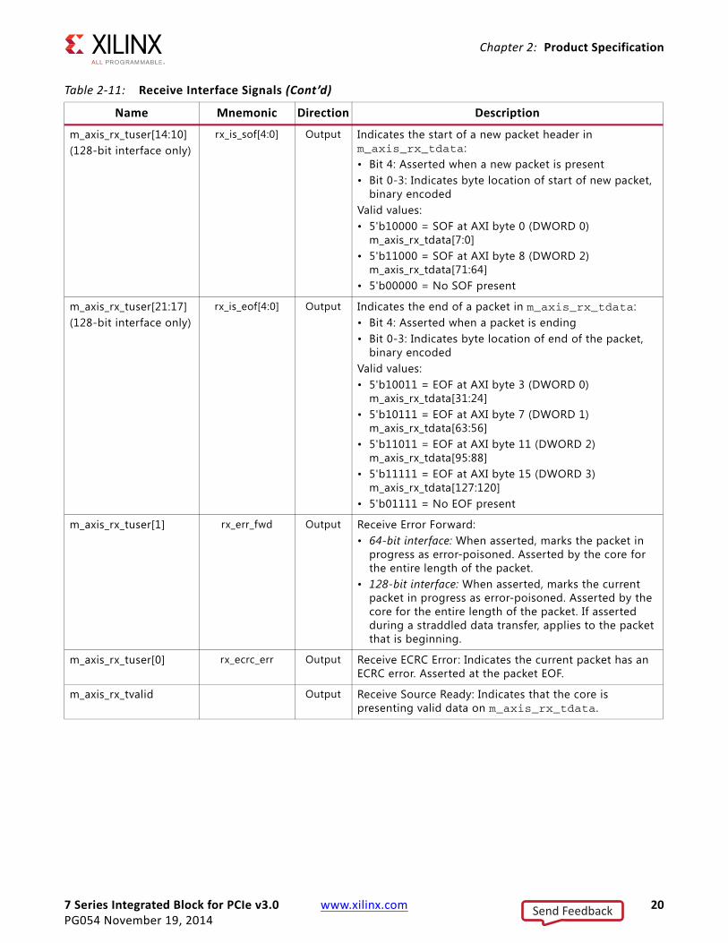
m_axis_rx_tuser[14:10](128-bit interface only)
rx_is_sof[4:0] Output Indicates the start of a new packet header in m_axis_rx_tdata: • Bit 4: Asserted when a new packet is present• Bit 0-3: Indicates byte location of start of new packet,
binary encodedValid values:• 5'b10000 = SOF at AXI byte 0 (DWORD 0)
m_axis_rx_tdata[7:0]• 5'b11000 = SOF at AXI byte 8 (DWORD 2)
m_axis_rx_tdata[71:64]• 5'b00000 = No SOF present
m_axis_rx_tuser[21:17](128-bit interface only)
rx_is_eof[4:0] Output Indicates the end of a packet in m_axis_rx_tdata: • Bit 4: Asserted when a packet is ending• Bit 0-3: Indicates byte location of end of the packet,
binary encodedValid values:• 5'b10011 = EOF at AXI byte 3 (DWORD 0)
m_axis_rx_tdata[31:24]• 5'b10111 = EOF at AXI byte 7 (DWORD 1)
m_axis_rx_tdata[63:56]• 5'b11011 = EOF at AXI byte 11 (DWORD 2)
m_axis_rx_tdata[95:88]• 5'b11111 = EOF at AXI byte 15 (DWORD 3)
m_axis_rx_tdata[127:120]• 5'b01111 = No EOF present
m_axis_rx_tuser[1] rx_err_fwd Output Receive Error Forward: • 64-bit interface: When asserted, marks the packet in
progress as error-poisoned. Asserted by the core for the entire length of the packet.
• 128-bit interface: When asserted, marks the current packet in progress as error-poisoned. Asserted by the core for the entire length of the packet. If asserted during a straddled data transfer, applies to the packet that is beginning.
m_axis_rx_tuser[0] rx_ecrc_err Output Receive ECRC Error: Indicates the current packet has an ECRC error. Asserted at the packet EOF.
m_axis_rx_tvalid Output Receive Source Ready: Indicates that the core is presenting valid data on m_axis_rx_tdata.
Table 2-11: Receive Interface Signals (Cont’d)
Name Mnemonic Direction Description
Send Feedback

7 Series Integrated Block for PCIe v3.0 www.xilinx.com 21PG054 November 19, 2014
Chapter 2: Product Specification
m_axis_rx_tready Input Receive Destination Ready: Indicates that the user application is ready to accept data on m_axis_rx_tdata. The simultaneous assertion of m_axis_rx_tvalid and m_axis_rx_tready marks the successful transfer of one data beat on s_axis_tx_tdata. For a Root port configuration, when a Legacy Interrupt is sent from the Endpoint, the ENABLE_MSG_ROUTE attribute should be set to 11'b00000001000 to see this signal toggling along with m_axis_rx_tdata, m_axis_rx_tkeep and m_axis_rx_tuser.
rx_np_ok Input Receive Non-Posted OK: The user application asserts this signal when it is ready to accept Non-Posted Request TLPs. rx_np_ok must be deasserted when the user application cannot process received Non-Posted TLPs, so that these can be buffered within the receive queue of the core. In this case, Posted and Completion TLPs received after the Non-Posted TLPs bypass the blocked TLPs.When the user application approaches a state where it is unable to service Non-Posted Requests, it must deassert rx_np_ok two clock cycle before the core asserts m_axis_rx_tlast of the next-to-last Non-Posted TLP the user application can accept.
rx_np_req Input Receive Non-Posted Request: When asserted, requests one non-posted TLP from the core per user_clk cycle. If the user application can process received Non-Posted TLPs at the line rate, this signal can be constantly asserted. If the user application is not requesting Non-Posted packets, received Posted and Completion TLPs bypass waiting Non-Posted TLPs.
m_axis_rx_tuser[9:2] rx_bar_hit[7:0] Output Receive BAR Hit: Indicates BAR(s) targeted by the current receive transaction. Asserted from the beginning of the packet to m_axis_rx_tlast.• (rx_bar_hit[0])m_axis_rx_tuser[2]: BAR0• (rx_bar_hit[1])m_axis_rx_tuser[3]: BAR1• (rx_bar_hit[2])m_axis_rx_tuser[4]: BAR2• (rx_bar_hit[3])m_axis_rx_tuser[5]: BAR3• (rx_bar_hit[4])m_axis_rx_tuser[6]: BAR4• (rx_bar_hit[5])m_axis_rx_tuser[7]: BAR5• (rx_bar_hit[6])m_axis_rx_tuser[8]: Expansion ROM
AddressIf two BARs are configured into a single 64-bit address, both corresponding rx_bar_hit bits are asserted.• m_axis_rx_tuser[8:4] are not applicable to Root
Port configurations.• m_axis_rx_tuser[9] is reserved for future use.
m_axis_rx_tuser[16:15] Reserved
Table 2-11: Receive Interface Signals (Cont’d)
Name Mnemonic Direction Description
Send Feedback

7 Series Integrated Block for PCIe v3.0 www.xilinx.com 22PG054 November 19, 2014
Chapter 2: Product Specification
Physical Layer InterfaceThe Physical Layer (PL) interface enables the user design to inspect the status of the Link and Link Partner and control the Link State. Table 2-12 describes the signals for the PL interface.
Table 2-12: Physical Layer Interface Signals
Name Direction Description
pl_initial_link_width[2:0] Output Initial Negotiated Link Width: Indicates the link width after the PCI Express port has achieved the f irst successful link training. Initial Negotiated Link Width represents the widest link width possible during normal operation of the link, and can be equal to or smaller than the capability link width (smaller of the two) supported by link partners. This value is reset when the core is reset or the LTSSM goes through the Detect state. Otherwise the value remains the same.• 000: Link not trained• 001: 1-Lane link• 010: 2-Lane link• 011: 4-Lane link• 100: 8-Lane link
pl_phy_lnk_up Output Physical Layer Link Up Status: Indicates the physical layer link up status.
pl_lane_reversal_mode[1:0] Output Lane Reversal Mode: Indicates the current Lane Reversal mode. • 00: No reversal• 01: Lanes 1:0 reversed• 10: Lanes 3:0 reversed• 11: Lanes 7:0 reversed
pl_link_gen2_cap Output Link Gen2 Capable: Indicates that the PCI Express link is 5.0 Gb/s (Gen 2) speed capable (both the Link Partner and the Device are Gen 2 capable)• 0: Link is not Gen2 Capable• 1: Link is Gen2 Capable
pl_link_partner_gen2_supported Output Link Partner Gen2 Capable: Indicates if the PCI Express link partner advertises 5.0 Gb/s (Gen2) capability. Valid only when user_lnk_up is asserted.• 0: Link partner not Gen2 capable• 1: Link partner is Gen2 capable
pl_link_upcfg_cap Output Link Upconfigure Capable: Indicates the PCI Express link is Upconfigure capable. Valid only when user_lnk_up is asserted.• 0: Link is not Upconfigure capable• 1: Link is Upconfigure capable
pl_sel_lnk_rate Output Current Link Rate: Reports the current link speed. Valid only when user_lnk_up is asserted.• 0: 2.5 Gb/s• 1: 5.0 Gb/s
Send Feedback
7 Series Integrated Block for PCIe v3.0 www.xilinx.com 23PG054 November 19, 2014
Chapter 2: Product Specification
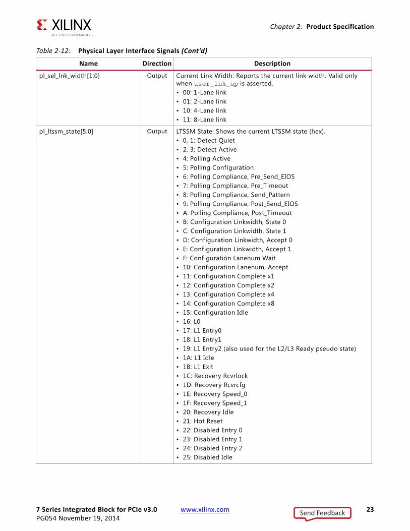
pl_sel_lnk_width[1:0] Output Current Link Width: Reports the current link width. Valid only when user_lnk_up is asserted.• 00: 1-Lane link• 01: 2-Lane link• 10: 4-Lane link• 11: 8-Lane link
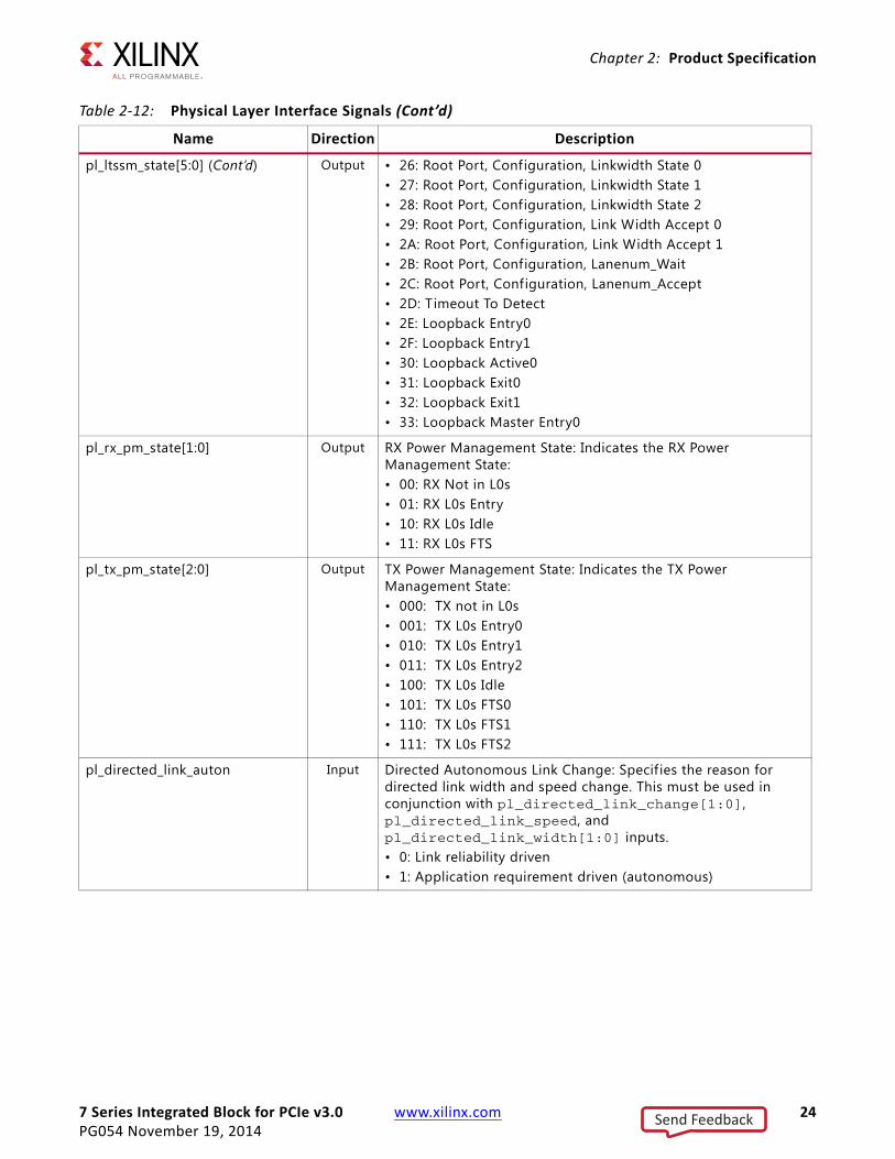
pl_ltssm_state[5:0] Output LTSSM State: Shows the current LTSSM state (hex).• 0, 1: Detect Quiet• 2, 3: Detect Active• 4: Polling Active• 5: Polling Configuration • 6: Polling Compliance, Pre_Send_EIOS • 7: Polling Compliance, Pre_Timeout • 8: Polling Compliance, Send_Pattern • 9: Polling Compliance, Post_Send_EIOS• A: Polling Compliance, Post_Timeout • B: Configuration Linkwidth, State 0 • C: Configuration Linkwidth, State 1 • D: Configuration Linkwidth, Accept 0 • E: Configuration Linkwidth, Accept 1 • F: Configuration Lanenum Wait • 10: Configuration Lanenum, Accept • 11: Configuration Complete x1 • 12: Configuration Complete x2• 13: Configuration Complete x4 • 14: Configuration Complete x8 • 15: Configuration Idle • 16: L0 • 17: L1 Entry0 • 18: L1 Entry1 • 19: L1 Entry2 (also used for the L2/L3 Ready pseudo state)• 1A: L1 Idle • 1B: L1 Exit • 1C: Recovery Rcvrlock • 1D: Recovery Rcvrcfg• 1E: Recovery Speed_0 • 1F: Recovery Speed_1 • 20: Recovery Idle • 21: Hot Reset • 22: Disabled Entry 0 • 23: Disabled Entry 1 • 24: Disabled Entry 2 • 25: Disabled Idle
Table 2-12: Physical Layer Interface Signals (Cont’d)
Name Direction Description
Send Feedback
7 Series Integrated Block for PCIe v3.0 www.xilinx.com 24PG054 November 19, 2014
Chapter 2: Product Specification
pl_ltssm_state[5:0] (Cont’d) Output • 26: Root Port, Configuration, Linkwidth State 0 • 27: Root Port, Configuration, Linkwidth State 1• 28: Root Port, Configuration, Linkwidth State 2• 29: Root Port, Configuration, Link Width Accept 0 • 2A: Root Port, Configuration, Link Width Accept 1 • 2B: Root Port, Configuration, Lanenum_Wait • 2C: Root Port, Configuration, Lanenum_Accept • 2D: Timeout To Detect • 2E: Loopback Entry0 • 2F: Loopback Entry1 • 30: Loopback Active0 • 31: Loopback Exit0 • 32: Loopback Exit1 • 33: Loopback Master Entry0
pl_rx_pm_state[1:0] Output RX Power Management State: Indicates the RX Power Management State:• 00: RX Not in L0s• 01: RX L0s Entry• 10: RX L0s Idle• 11: RX L0s FTS
pl_tx_pm_state[2:0] Output TX Power Management State: Indicates the TX Power Management State:• 000: TX not in L0s • 001: TX L0s Entry0 • 010: TX L0s Entry1 • 011: TX L0s Entry2 • 100: TX L0s Idle • 101: TX L0s FTS0 • 110: TX L0s FTS1 • 111: TX L0s FTS2
pl_directed_link_auton Input Directed Autonomous Link Change: Specif ies the reason for directed link width and speed change. This must be used in conjunction with pl_directed_link_change[1:0], pl_directed_link_speed, and pl_directed_link_width[1:0] inputs.• 0: Link reliability driven• 1: Application requirement driven (autonomous)
Table 2-12: Physical Layer Interface Signals (Cont’d)
Name Direction Description
Send Feedback

7 Series Integrated Block for PCIe v3.0 www.xilinx.com 25PG054 November 19, 2014
Chapter 2: Product Specification
pl_directed_link_change[1:0] Input Directed Link Change Control: Directs the PCI Express Port to initiate a link width and/or speed change. Link change operation must be initiated when user_lnk_up is asserted. For a Root Port, pl_directed_link_change must not be set to 10 or 11 unless the attribute RP_AUTO_SPD = 11.• 00: No change• 01: Link width• 10: Link speed• 11: Link width and speed (level-triggered)
pl_directed_link_speed Input Directed Target Link Speed: Specif ies the target link speed for a directed link change operation, in conjunction with the pl_directed_link_change[1:0] input. The target link speed must not be set High unless the pl_link_gen2_capable output is High.• 0: 2.5 Gb/s• 1: 5.0 Gb/s
pl_directed_link_width[1:0] Input Directed Target Link Width: Specif ies the target link width for a directed link change operation, in conjunction with pl_directed_link_change[1:0] input.Encoding Target Link Width:• 00: 1-Lane link• 01: 2-Lane link• 10: 4-Lane link• 11: 8-Lane link
pl_directed_change_done Output Directed Link Change Done: Indicates to the user application that the directed link speed change or directed link width change is done.
pl_upstream_prefer_deemph Input Endpoint Preferred Transmitter De-emphasis: Enables the Endpoint to control de-emphasis used on the link at 5.0 Gb/s speeds. pl_upstream_prefer_deemph can be changed in conjunction with pl_directed_link_speed and pl_directed_link_change[1:0] inputs when transitioning from 2.5 Gb/s to 5.0 Gb/s data rates. Value presented on pl_upstream_prefer_deemph depends upon the property of PCI Express physical interconnect channel in use. • 0: –6 dB de-emphasis recommended for short, reflection
dominated channels.• 1: –3.5 dB de-emphasis recommended for long, loss dominated
channels.
Table 2-12: Physical Layer Interface Signals (Cont’d)
Name Direction Description
Table 2-13: Role-Specific Physical Layer Interface Signals: Endpoint
Name Direction Description
pl_received_hot_rst Output Hot Reset Received: Indicates that an in-band hot reset command has been received.
Send Feedback
7 Series Integrated Block for PCIe v3.0 www.xilinx.com 26PG054 November 19, 2014
Chapter 2: Product Specification
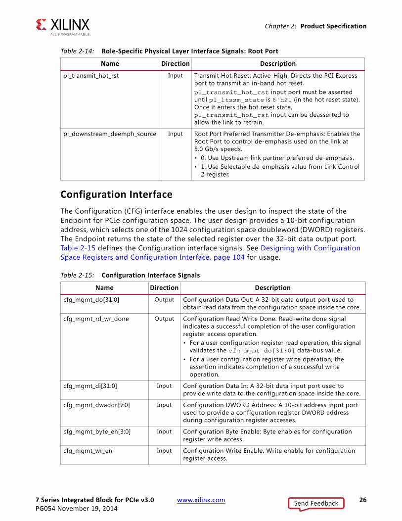
Configuration InterfaceThe Configuration (CFG) interface enables the user design to inspect the state of the Endpoint for PCIe configuration space. The user design provides a 10-bit configuration address, which selects one of the 1024 configuration space doubleword (DWORD) registers. The Endpoint returns the state of the selected register over the 32-bit data output port. Table 2-15 defines the Configuration interface signals. See Designing with Configuration Space Registers and Configuration Interface, page 104 for usage.
Table 2-14: Role-Specific Physical Layer Interface Signals: Root Port
Name Direction Description
pl_transmit_hot_rst Input Transmit Hot Reset: Active-High. Directs the PCI Express port to transmit an in-band hot reset.pl_transmit_hot_rst input port must be asserted until pl_ltssm_state is 6'h21 (in the hot reset state). Once it enters the hot reset state, pl_transmit_hot_rst input can be deasserted to allow the link to retrain.
pl_downstream_deemph_source Input Root Port Preferred Transmitter De-emphasis: Enables the Root Port to control de-emphasis used on the link at 5.0 Gb/s speeds.• 0: Use Upstream link partner preferred de-emphasis.• 1: Use Selectable de-emphasis value from Link Control
2 register.
Table 2-15: Configuration Interface Signals
Name Direction Description
cfg_mgmt_do[31:0] Output Configuration Data Out: A 32-bit data output port used to obtain read data from the configuration space inside the core.
cfg_mgmt_rd_wr_done Output Configuration Read Write Done: Read-write done signal indicates a successful completion of the user configuration register access operation. • For a user configuration register read operation, this signal
validates the cfg_mgmt_do[31:0] data-bus value. • For a user configuration register write operation, the
assertion indicates completion of a successful write operation.
cfg_mgmt_di[31:0] Input Configuration Data In: A 32-bit data input port used to provide write data to the configuration space inside the core.
cfg_mgmt_dwaddr[9:0] Input Configuration DWORD Address: A 10-bit address input port used to provide a configuration register DWORD address during configuration register accesses.
cfg_mgmt_byte_en[3:0] Input Configuration Byte Enable: Byte enables for configuration register write access.
cfg_mgmt_wr_en Input Configuration Write Enable: Write enable for configuration register access.
Send Feedback

7 Series Integrated Block for PCIe v3.0 www.xilinx.com 27PG054 November 19, 2014
Chapter 2: Product Specification
cfg_mgmt_rd_en Input Configuration Read Enable: Read enable for configuration register access.
cfg_mgmt_wr_readonly Input Management Write Readonly Bits: Write enable to treat any ReadOnly bit in the current Management Write as a RW bit, not including bits set by attributes, reserved bits, and status bits.
cfg_status[15:0] Output Configuration Status: Status register from the Configuration Space Header. Not supported.
cfg_command[15:0] Output Configuration Command: Command register from the Configuration Space Header.
cfg_dstatus[15:0] Output Configuration Device Status: Device status register from the PCI Express Capability Structure.
cfg_dcommand[15:0] Output Configuration Device Command: Device control register from the PCI Express Capability Structure.
cfg_dcommand2[15:0] Output Configuration Device Command 2: Device control 2 register from the PCI Express Capability Structure.
cfg_lstatus[15:0] Output Configuration Link Status: Link status register from the PCI Express Capability Structure.
cfg_lcommand[15:0] Output Configuration Link Command: Link control register from the PCI Express Capability Structure.
cfg_aer_ecrc_gen_en Output Configuration AER - ECRC Generation Enable: AER Capability and Control Register bit 6. When asserted, indicates that ECRC Generation has been enabled by the host.
cfg_aer_ecrc_check_en Output Configuration AER - ECRC Check Enable: AER Capability and Control Register bit 8. When asserted, indicates that ECRC Checking has been enabled by the host.
cfg_pcie_link_state[2:0] Output PCI Express Link State: This encoded bus reports the PCI Express Link State information.• 000: L0• 001: PPM L1• 010: PPM L2/L3 Ready• 011: PM_PME• 100: in or transitioning to/from ASPM L0s• 101: transitioning to/from PPM L1• 110: transition to PPM L2/L3 Ready• 111: Reserved
cfg_trn_pending Input User Transaction Pending: If asserted, sets the Transactions Pending bit in the Device Status Register. Note: You must assert this input if the user application has not received a completion to an upstream request.
cfg_dsn[63:0] Input Configuration Device Serial Number: Serial Number Register f ields of the Device Serial Number extended capability.
cfg_pmcsr_pme_en Output PMCSR PME Enable: PME_En bit (bit 8) in the Power Management Control/Status Register.
Table 2-15: Configuration Interface Signals (Cont’d)
Name Direction Description
Send Feedback
7 Series Integrated Block for PCIe v3.0 www.xilinx.com 28PG054 November 19, 2014
Chapter 2: Product Specification
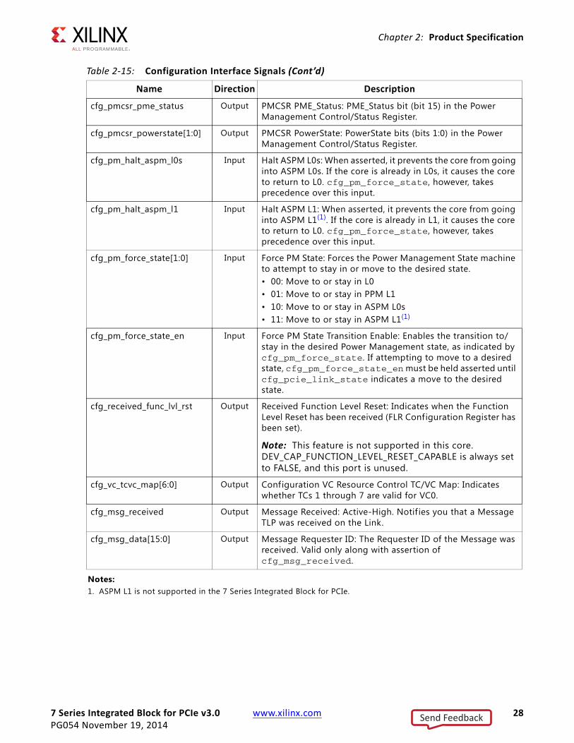
cfg_pmcsr_pme_status Output PMCSR PME_Status: PME_Status bit (bit 15) in the Power Management Control/Status Register.
cfg_pmcsr_powerstate[1:0] Output PMCSR PowerState: PowerState bits (bits 1:0) in the Power Management Control/Status Register.
cfg_pm_halt_aspm_l0s Input Halt ASPM L0s: When asserted, it prevents the core from going into ASPM L0s. If the core is already in L0s, it causes the core to return to L0. cfg_pm_force_state, however, takes precedence over this input.
cfg_pm_halt_aspm_l1 Input Halt ASPM L1: When asserted, it prevents the core from going into ASPM L1(1). If the core is already in L1, it causes the core to return to L0. cfg_pm_force_state, however, takes precedence over this input.
cfg_pm_force_state[1:0] Input Force PM State: Forces the Power Management State machine to attempt to stay in or move to the desired state.• 00: Move to or stay in L0 • 01: Move to or stay in PPM L1• 10: Move to or stay in ASPM L0s• 11: Move to or stay in ASPM L1(1)
cfg_pm_force_state_en Input Force PM State Transition Enable: Enables the transition to/stay in the desired Power Management state, as indicated by cfg_pm_force_state. If attempting to move to a desired state, cfg_pm_force_state_en must be held asserted until cfg_pcie_link_state indicates a move to the desired state.
cfg_received_func_lvl_rst Output Received Function Level Reset: Indicates when the Function Level Reset has been received (FLR Configuration Register has been set).
Note: This feature is not supported in this core. DEV_CAP_FUNCTION_LEVEL_RESET_CAPABLE is always set to FALSE, and this port is unused.
cfg_vc_tcvc_map[6:0] Output Configuration VC Resource Control TC/VC Map: Indicates whether TCs 1 through 7 are valid for VC0.
cfg_msg_received Output Message Received: Active-High. Notif ies you that a Message TLP was received on the Link.
cfg_msg_data[15:0] Output Message Requester ID: The Requester ID of the Message was received. Valid only along with assertion of cfg_msg_received.
Notes: 1. ASPM L1 is not supported in the 7 Series Integrated Block for PCIe.
Table 2-15: Configuration Interface Signals (Cont’d)
Name Direction Description
Send Feedback
7 Series Integrated Block for PCIe v3.0 www.xilinx.com 29PG054 November 19, 2014
Chapter 2: Product Specification
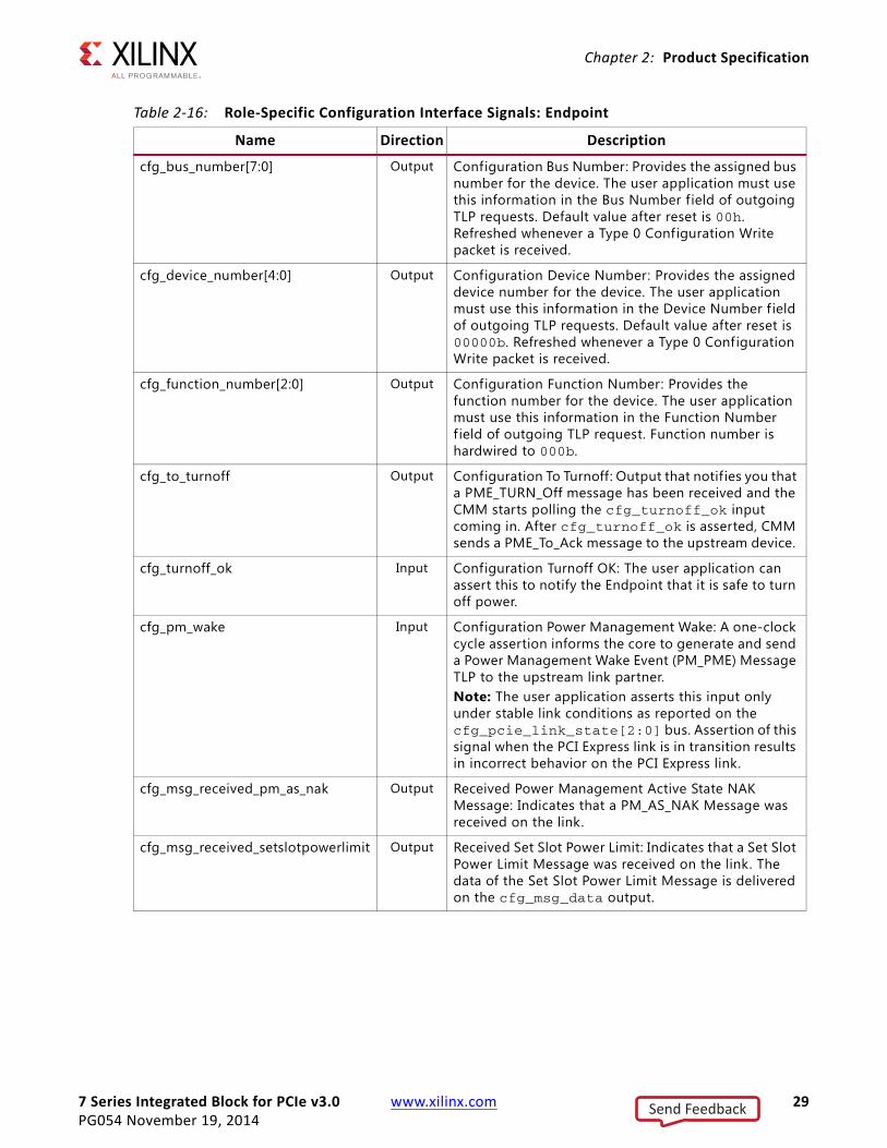
Table 2-16: Role-Specific Configuration Interface Signals: Endpoint
Name Direction Description
cfg_bus_number[7:0] Output Configuration Bus Number: Provides the assigned bus number for the device. The user application must use this information in the Bus Number field of outgoing TLP requests. Default value after reset is 00h. Refreshed whenever a Type 0 Configuration Write packet is received.
cfg_device_number[4:0] Output Configuration Device Number: Provides the assigned device number for the device. The user application must use this information in the Device Number f ield of outgoing TLP requests. Default value after reset is 00000b. Refreshed whenever a Type 0 Configuration Write packet is received.
cfg_function_number[2:0] Output Configuration Function Number: Provides the function number for the device. The user application must use this information in the Function Number f ield of outgoing TLP request. Function number is hardwired to 000b.
cfg_to_turnoff Output Configuration To Turnoff: Output that notif ies you that a PME_TURN_Off message has been received and the CMM starts polling the cfg_turnoff_ok input coming in. After cfg_turnoff_ok is asserted, CMM sends a PME_To_Ack message to the upstream device.
cfg_turnoff_ok Input Configuration Turnoff OK: The user application can assert this to notify the Endpoint that it is safe to turn off power.
cfg_pm_wake Input Configuration Power Management Wake: A one-clock cycle assertion informs the core to generate and send a Power Management Wake Event (PM_PME) Message TLP to the upstream link partner. Note: The user application asserts this input only under stable link conditions as reported on the cfg_pcie_link_state[2:0] bus. Assertion of this signal when the PCI Express link is in transition results in incorrect behavior on the PCI Express link.
cfg_msg_received_pm_as_nak Output Received Power Management Active State NAK Message: Indicates that a PM_AS_NAK Message was received on the link.
cfg_msg_received_setslotpowerlimit Output Received Set Slot Power Limit: Indicates that a Set Slot Power Limit Message was received on the link. The data of the Set Slot Power Limit Message is delivered on the cfg_msg_data output.
Send Feedback

7 Series Integrated Block for PCIe v3.0 www.xilinx.com 30PG054 November 19, 2014
Chapter 2: Product Specification
Table 2-17: Role-Specific Configuration Interface Signals: Root Port
Name Direction Description
cfg_ds_bus_number[7:0] Input Configuration Downstream Bus Number: Provides the bus number (Requester ID) of the Downstream Port. This is used in TLPs generated inside the core and does not affect the TLPs presented on the AXI4-Stream interface.
cfg_ds_device_number[4:0] Input Configuration Downstream Device Number: Provides the device number (Requester ID) of the Downstream Port. This is used in TLPs generated inside the core and does not affect the TLPs presented on the transaction interface.
cfg_ds_function_number[2:0] Input Configuration Downstream Function Number: Provides the function number (Requester ID) of the Downstream Port. This is used in TLPs generated inside the core and does not affect the TLPs presented on the transaction interface.
cfg_wr_rw1c_as_rw Input Configuration Write RW1C Bit as RW: Indicates that the current write operation should treat any RW1C bit as a RW bit. Normally, a RW1C bit is cleared by writing a 1 to it, and can normally only be set by internal core conditions. However, during a configuration register access operation with this signal asserted, for every bit on cfg_di that is 1, the corresponding RW1C configuration register bit is set to 1. A value of 0 on cfg_di during this operation has no effect, and non-RW1C bits are unaffected regardless of the value on cfg_di.
cfg_msg_received_err_cor Output Received ERR_COR Message: Active-High. Indicates that the core received an ERR_COR Message. Valid only along with assertion of cfg_msg_received. The Requester ID of this Message Transaction is provided on cfg_msg_data[15:0].
cfg_msg_received_err_non_fatal Output Received ERR_NONFATAL Message: Active-High. Indicates that the core received an ERR_NONFATAL Message. Valid only along with assertion of cfg_msg_received. The Requester ID of this Message Transaction is provided on cfg_msg_data[15:0].
cfg_msg_received_err_fatal Output Received ERR_FATAL Message: Active-High. Indicates that the core received an ERR_FATAL Message. Valid only along with assertion of cfg_msg_received. The Requester ID of this Message Transaction is provided on cfg_msg_data[15:0].
cfg_pm_send_pme_to Input Configuration Send Turn-off: Asserting this active-Low input causes the Root Port to send Turn Off Message. When the link partner responds with a Turn Off Ack, this is reported on cfg_msg_received_pme_to_ack, and the final transition to L3 Ready is reported on cfg_pcie_link_state. Tie-off to 1 for Endpoint.
Send Feedback
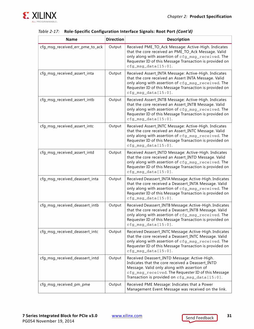
7 Series Integrated Block for PCIe v3.0 www.xilinx.com 31PG054 November 19, 2014
Chapter 2: Product Specification
cfg_msg_received_err_pme_to_ack Output Received PME_TO_Ack Message: Active-High. Indicates that the core received an PME_TO_Ack Message. Valid only along with assertion of cfg_msg_received. The Requester ID of this Message Transaction is provided on cfg_msg_data[15:0].
cfg_msg_received_assert_inta Output Received Assert_INTA Message: Active-High. Indicates that the core received an Assert INTA Message. Valid only along with assertion of cfg_msg_received. The Requester ID of this Message Transaction is provided on cfg_msg_data[15:0].
cfg_msg_received_assert_intb Output Received Assert_INTB Message: Active-High. Indicates that the core received an Assert_INTB Message. Valid only along with assertion of cfg_msg_received. The Requester ID of this Message Transaction is provided on cfg_msg_data[15:0].
cfg_msg_received_assert_intc Output Received Assert_INTC Message: Active-High. Indicates that the core received an Assert_INTC Message. Valid only along with assertion of cfg_msg_received. The Requester ID of this Message Transaction is provided on cfg_msg_data[15:0].
cfg_msg_received_assert_intd Output Received Assert_INTD Message: Active-High. Indicates that the core received an Assert_INTD Message. Valid only along with assertion of cfg_msg_received. The Requester ID of this Message Transaction is provided on cfg_msg_data[15:0].
cfg_msg_received_deassert_inta Output Received Deassert_INTA Message: Active-High. Indicates that the core received a Deassert_INTA Message. Valid only along with assertion of cfg_msg_received. The Requester ID of this Message Transaction is provided on cfg_msg_data[15:0].
cfg_msg_received_deassert_intb Output Received Deassert_INTB Message: Active-High. Indicates that the core received a Deassert_INTB Message. Valid only along with assertion of cfg_msg_received. The Requester ID of this Message Transaction is provided on cfg_msg_data[15:0].
cfg_msg_received_deassert_intc Output Received Deassert_INTC Message: Active-High. Indicates that the core received a Deassert_INTC Message. Valid only along with assertion of cfg_msg_received. The Requester ID of this Message Transaction is provided on cfg_msg_data[15:0].
cfg_msg_received_deassert_intd Output Received Deassert_INTD Message: Active-High. Indicates that the core received a Deassert_INTD Message. Valid only along with assertion of cfg_msg_received. The Requester ID of this Message Transaction is provided on cfg_msg_data[15:0].
cfg_msg_received_pm_pme Output Received PME Message: Indicates that a Power Management Event Message was received on the link.
Table 2-17: Role-Specific Configuration Interface Signals: Root Port (Cont’d)
Name Direction Description
Send Feedback
7 Series Integrated Block for PCIe v3.0 www.xilinx.com 32PG054 November 19, 2014
Chapter 2: Product Specification
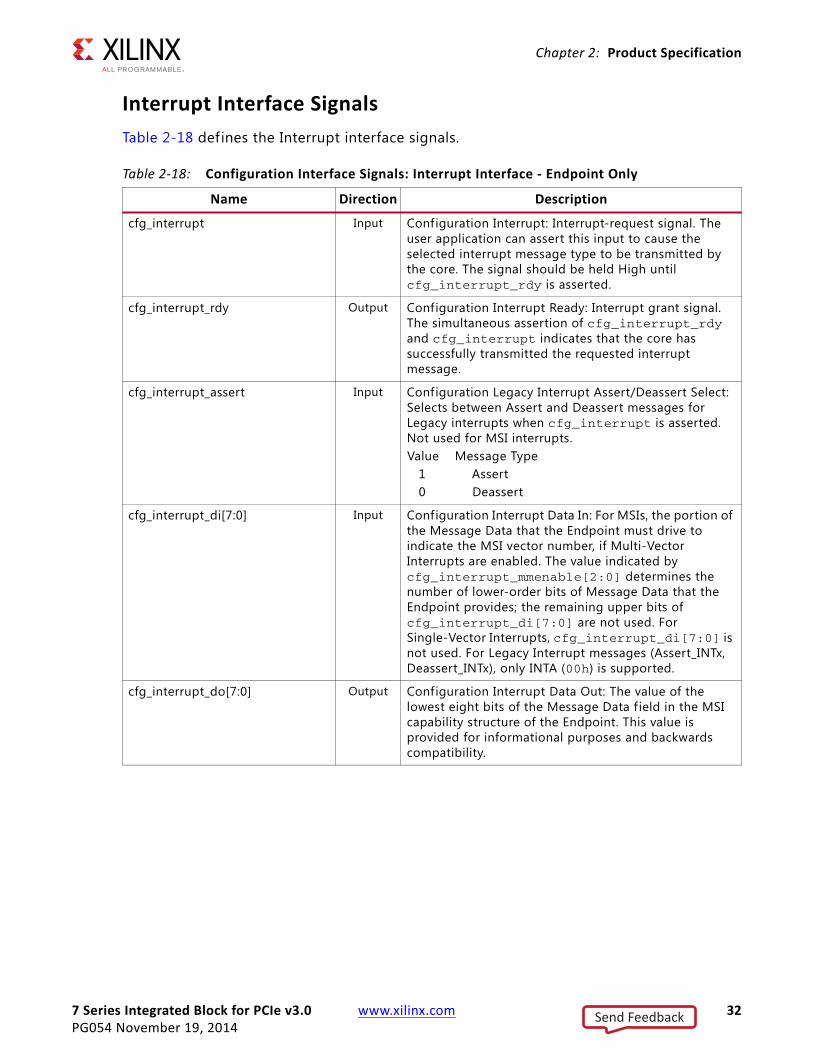
Interrupt Interface SignalsTable 2-18 defines the Interrupt interface signals.
Table 2-18: Configuration Interface Signals: Interrupt Interface - Endpoint Only
Name Direction Description
cfg_interrupt Input Configuration Interrupt: Interrupt-request signal. The user application can assert this input to cause the selected interrupt message type to be transmitted by the core. The signal should be held High until cfg_interrupt_rdy is asserted.
cfg_interrupt_rdy Output Configuration Interrupt Ready: Interrupt grant signal. The simultaneous assertion of cfg_interrupt_rdy and cfg_interrupt indicates that the core has successfully transmitted the requested interrupt message.
cfg_interrupt_assert Input Configuration Legacy Interrupt Assert/Deassert Select: Selects between Assert and Deassert messages for Legacy interrupts when cfg_interrupt is asserted. Not used for MSI interrupts.Value Message Type
1 Assert0 Deassert
cfg_interrupt_di[7:0] Input Configuration Interrupt Data In: For MSIs, the portion of the Message Data that the Endpoint must drive to indicate the MSI vector number, if Multi-Vector Interrupts are enabled. The value indicated by cfg_interrupt_mmenable[2:0] determines the number of lower-order bits of Message Data that the Endpoint provides; the remaining upper bits of cfg_interrupt_di[7:0] are not used. For Single-Vector Interrupts, cfg_interrupt_di[7:0] is not used. For Legacy Interrupt messages (Assert_INTx, Deassert_INTx), only INTA (00h) is supported.
cfg_interrupt_do[7:0] Output Configuration Interrupt Data Out: The value of the lowest eight bits of the Message Data f ield in the MSI capability structure of the Endpoint. This value is provided for informational purposes and backwards compatibility.
Send Feedback
7 Series Integrated Block for PCIe v3.0 www.xilinx.com 33PG054 November 19, 2014
Chapter 2: Product Specification
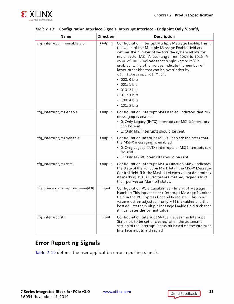
Error Reporting SignalsTable 2-19 defines the user application error-reporting signals.
cfg_interrupt_mmenable[2:0] Output Configuration Interrupt Multiple Message Enable: This is the value of the Multiple Message Enable f ield and defines the number of vectors the system allows for multi-vector MSI. Values range from 000b to 101b. A value of 000b indicates that single-vector MSI is enabled, while other values indicate the number of lower-order bits that can be overridden by cfg_interrupt_di[7:0].• 000: 0 bits• 001: 1 bit• 010: 2 bits• 011: 3 bits• 100: 4 bits• 101: 5 bits
cfg_interrupt_msienable Output Configuration Interrupt MSI Enabled: Indicates that MSI messaging is enabled.• 0: Only Legacy (INTX) interrupts or MSI-X Interrupts
can be sent.• 1: Only MSI Interrupts should be sent.
cfg_interrupt_msixenable Output Configuration Interrupt MSI-X Enabled: Indicates that the MSI-X messaging is enabled.• 0: Only Legacy (INTX) interrupts or MSI Interrupts can
be sent.• 1: Only MSI-X Interrupts should be sent.
cfg_interrupt_msixfm Output Configuration Interrupt MSI-X Function Mask: Indicates the state of the Function Mask bit in the MSI-X Message Control f ield. If 0, the Mask bit of each vector determines its masking. If 1, all vectors are masked, regardless of their per-vector Mask bit states.
cfg_pciecap_interrupt_msgnum[4:0] Input Configuration PCIe Capabilities - Interrupt Message Number: This input sets the Interrupt Message Number field in the PCI Express Capability register. This input value must be adjusted if only MSI is enabled and the host adjusts the Multiple Message Enable f ield such that it invalidates the current value.
cfg_interrupt_stat Input Configuration Interrupt Status: Causes the Interrupt Status bit to be set or cleared when the automatic setting of the Interrupt Status bit based on the Interrupt Interface inputs is disabled.
Table 2-18: Configuration Interface Signals: Interrupt Interface - Endpoint Only (Cont’d)
Name Direction Description
Send Feedback

7 Series Integrated Block for PCIe v3.0 www.xilinx.com 34PG054 November 19, 2014
Chapter 2: Product Specification
Table 2-19: User Application Error-Reporting Signals
Port Name Direction Description
cfg_err_ecrc Input ECRC Error Report: You can assert this signal to report an ECRC error (end-to-end CRC).
cfg_err_ur Input Configuration Error Unsupported Request: You can assert this signal to report that an unsupported request was received. This signal is ignored if cfg_err_cpl_rdy is deasserted.
cfg_err_cpl_timeout(1) Input Configuration Error Completion Timeout: You can assert this signal to report that a completion timed out.
cfg_err_cpl_unexpect Input Configuration Error Completion Unexpected: You can assert this signal to report that an unexpected completion was received.
cfg_err_cpl_abort Input Configuration Error Completion Aborted: You can assert this signal to report that a completion was aborted. This signal is ignored if cfg_err_cpl_rdy is deasserted.
cfg_err_posted Input Configuration Error Posted: This signal is used to further qualify any of the cfg_err_* input signals. When this input is asserted concurrently with one of the other signals, it indicates that the transaction that caused the error was a posted transaction.
cfg_err_cor(1) Input Configuration Error Correctable Error: You can assert this signal to report that a correctable error was detected.
cfg_err_atomic_egress_blocked Input Configuration Error AtomicOp Egress Blocked: You can assert this signal to report that an Atomic TLP was blocked.
cfg_err_internal_cor Input Configuration Error Corrected Internal: You can assert this signal to report that an Internal error occurred and was corrected. This input is only sampled if AER is enabled.
cfg_err_internal_uncor Input Configuration Error Uncorrectable Internal: You can assert this signal to report that an Uncorrectable Internal error occurred. This input is only sampled if AER is enabled.
cfg_err_malformed Input Configuration Error Malformed Error: You can assert this signal to report a Malformed Error.
cfg_err_mc_blocked Input Configuration Error MultiCast Blocked: You can assert this signal to report that a Multicast TLP was blocked.
cfg_err_poisoned Input Configuration Error Poisoned TLP: You can assert this signal to report that a Poisoned TLP was received. Normally, only used if attribute DISABLE_RX_POISONED_RESP=TRUE.
Send Feedback
7 Series Integrated Block for PCIe v3.0 www.xilinx.com 35PG054 November 19, 2014
Chapter 2: Product Specification
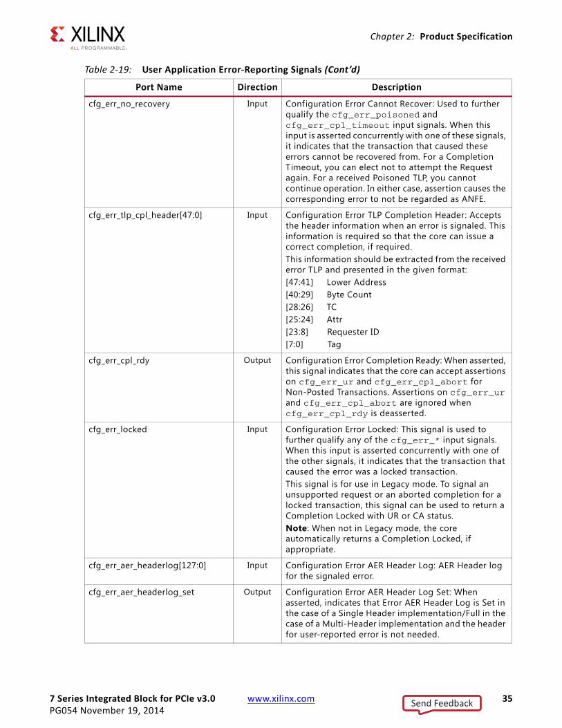
cfg_err_no_recovery Input Configuration Error Cannot Recover: Used to further qualify the cfg_err_poisoned and cfg_err_cpl_timeout input signals. When this input is asserted concurrently with one of these signals, it indicates that the transaction that caused these errors cannot be recovered from. For a Completion Timeout, you can elect not to attempt the Request again. For a received Poisoned TLP, you cannot continue operation. In either case, assertion causes the corresponding error to not be regarded as ANFE.
cfg_err_tlp_cpl_header[47:0] Input Configuration Error TLP Completion Header: Accepts the header information when an error is signaled. This information is required so that the core can issue a correct completion, if required. This information should be extracted from the received error TLP and presented in the given format:[47:41] Lower Address[40:29] Byte Count[28:26] TC[25:24] Attr[23:8] Requester ID[7:0] Tag
cfg_err_cpl_rdy Output Configuration Error Completion Ready: When asserted, this signal indicates that the core can accept assertions on cfg_err_ur and cfg_err_cpl_abort for Non-Posted Transactions. Assertions on cfg_err_ur and cfg_err_cpl_abort are ignored when cfg_err_cpl_rdy is deasserted.
cfg_err_locked Input Configuration Error Locked: This signal is used to further qualify any of the cfg_err_* input signals. When this input is asserted concurrently with one of the other signals, it indicates that the transaction that caused the error was a locked transaction. This signal is for use in Legacy mode. To signal an unsupported request or an aborted completion for a locked transaction, this signal can be used to return a Completion Locked with UR or CA status.Note: When not in Legacy mode, the core automatically returns a Completion Locked, if appropriate.
cfg_err_aer_headerlog[127:0] Input Configuration Error AER Header Log: AER Header log for the signaled error.
cfg_err_aer_headerlog_set Output Configuration Error AER Header Log Set: When asserted, indicates that Error AER Header Log is Set in the case of a Single Header implementation/Full in the case of a Multi-Header implementation and the header for user-reported error is not needed.
Table 2-19: User Application Error-Reporting Signals (Cont’d)
Port Name Direction Description
Send Feedback
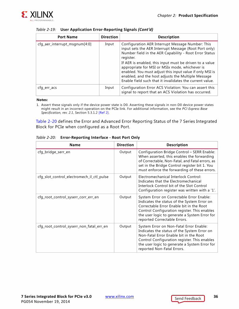
7 Series Integrated Block for PCIe v3.0 www.xilinx.com 36PG054 November 19, 2014
Chapter 2: Product Specification
Table 2-20 defines the Error and Advanced Error Reporting Status of the 7 Series Integrated Block for PCIe when configured as a Root Port.
cfg_aer_interrupt_msgnum[4:0] Input Configuration AER Interrupt Message Number: This input sets the AER Interrupt Message (Root Port only) Number f ield in the AER Capability - Root Error Status register. If AER is enabled, this input must be driven to a value appropriate for MSI or MSIx mode, whichever is enabled. You must adjust this input value if only MSI is enabled, and the host adjusts the Multiple Message Enable field such that it invalidates the current value.
cfg_err_acs Input Configuration Error ACS Violation: You can assert this signal to report that an ACS Violation has occurred.
Notes: 1. Assert these signals only if the device power state is D0. Asserting these signals in non-D0 device power states
might result in an incorrect operation on the PCIe link. For additional information, see the PCI Express Base Specification, rev. 2.1, Section 5.3.1.2 [Ref 2].
Table 2-20: Error-Reporting Interface - Root Port Only
Name Direction Description
cfg_bridge_serr_en Output Configuration Bridge Control – SERR Enable: When asserted, this enables the forwarding of Correctable, Non-Fatal, and Fatal errors, as set in the Bridge Control register bit 1. You must enforce the forwarding of these errors.
cfg_slot_control_electromech_il_ctl_pulse Output Electromechanical Interlock Control: Indicates that the Electromechanical Interlock Control bit of the Slot Control Configuration register was written with a ‘1’.
cfg_root_control_syserr_corr_err_en Output System Error on Correctable Error Enable: Indicates the status of the System Error on Correctable Error Enable bit in the Root Control Configuration register. This enables the user logic to generate a System Error for reported Correctable Errors.
cfg_root_control_syserr_non_fatal_err_en Output System Error on Non-Fatal Error Enable: Indicates the status of the System Error on Non-Fatal Error Enable bit in the Root Control Configuration register. This enables the user logic to generate a System Error for reported Non-Fatal Errors.
Table 2-19: User Application Error-Reporting Signals (Cont’d)
Port Name Direction Description
Send Feedback

7 Series Integrated Block for PCIe v3.0 www.xilinx.com 37PG054 November 19, 2014
Chapter 2: Product Specification
cfg_root_control_syserr_fatal_err_en Output System Error on Fatal Error Enable: Indicates the status of the System Error on Fatal Error Enable bit in the Root Control Configuration register. This enables the user logic to generate a System Error for reported Fatal Errors.
cfg_root_control_pme_int_en Output PME Interrupt Enable: Indicates the status of the PME Interrupt Enable bit in the Root Control Configuration register. This enables the user logic to generate an Interrupt for received PME messages.
cfg_aer_rooterr_corr_err_reporting_en Output AER Correctable Error Reporting Enable: Indicates status of the AER Correctable Error Reporting Enable bit in the AER Root Error Command configuration register. This bit enables the user logic to generate Interrupts for reported Correctable Errors.
cfg_aer_rooterr_non_fatal_err_reporting_en Output AER Non-Fatal Error Reporting Enable: Indicates status of the AER Non-Fatal Error Reporting Enable bit in the AER Root Error Command configuration register. This bit enables the user logic to generate Interrupts for reported Non-Fatal Errors.
cfg_aer_rooterr_fatal_err_reporting_en Output AER Fatal Error Reporting Enable: Indicates status of the AER Fatal Error Reporting Enable bit in the AER Root Error Command configuration register. This bit enables the user logic to generate Interrupts for reported Fatal Errors.
cfg_aer_rooterr_corr_err_received Output AER Correctable Error Message Received: Indicates status of the AER Correctable Error Message Received bit in the AER Root Error Status configuration register. This bit indicates that a Correctable Error message was received.
cfg_aer_rooterr_non_fatal_err_received Output AER Non-Fatal Error Message Received: Indicates status of the AER Non-Fatal Error Message Received bit in the AER Root Error Status configuration register. This bit indicates that a Non-Fatal Error message was received.
cfg_aer_rooterr_fatal_err_received Output AER Fatal Error Message Received: Indicates status of the AER Fatal Error Message Received bit in the AER Root Error Status configuration register. This bit indicates that a Fatal Error message was received.
Table 2-20: Error-Reporting Interface - Root Port Only (Cont’d)
Name Direction Description
Send Feedback
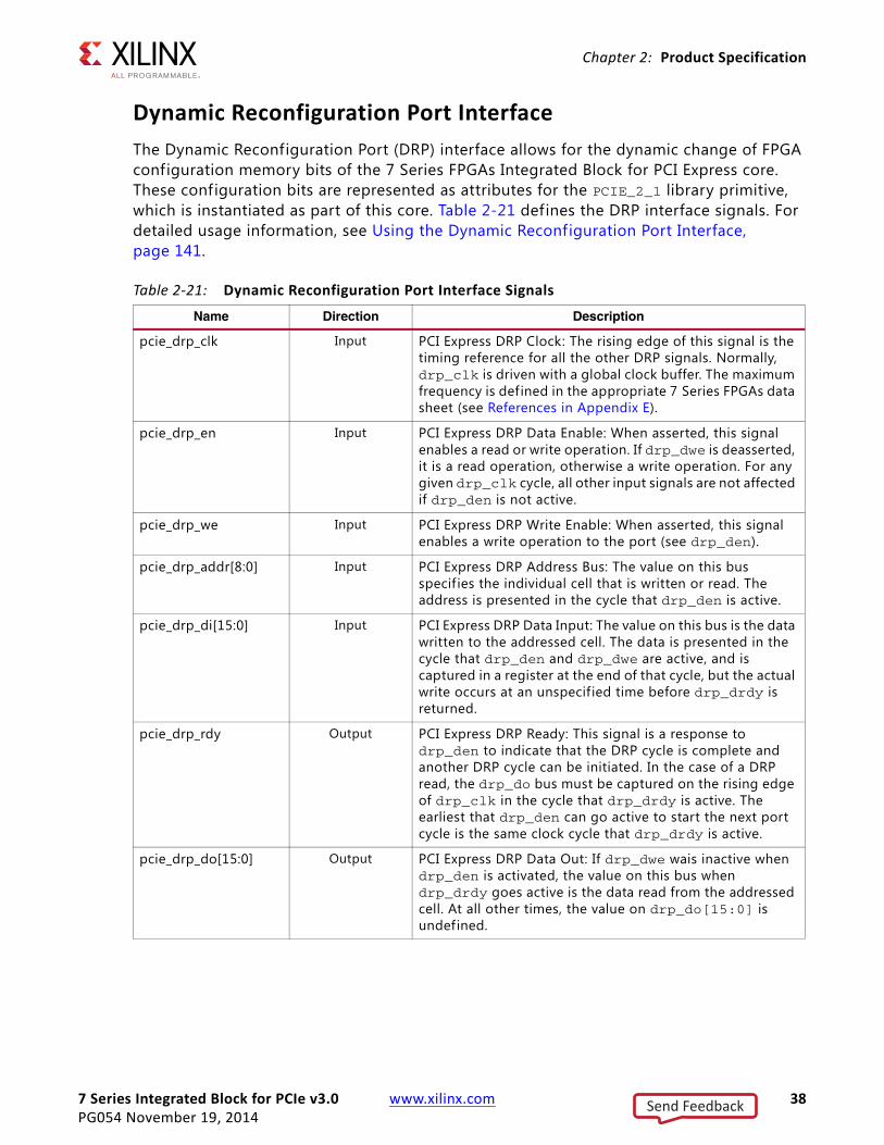
7 Series Integrated Block for PCIe v3.0 www.xilinx.com 38PG054 November 19, 2014
Chapter 2: Product Specification
Dynamic Reconfiguration Port InterfaceThe Dynamic Reconfiguration Port (DRP) interface allows for the dynamic change of FPGA configuration memory bits of the 7 Series FPGAs Integrated Block for PCI Express core. These configuration bits are represented as attributes for the PCIE_2_1 library primitive, which is instantiated as part of this core. Table 2-21 defines the DRP interface signals. For detailed usage information, see Using the Dynamic Reconfiguration Port Interface, page 141.
Table 2-21: Dynamic Reconfiguration Port Interface Signals
Name Direction Description
pcie_drp_clk Input PCI Express DRP Clock: The rising edge of this signal is the timing reference for all the other DRP signals. Normally, drp_clk is driven with a global clock buffer. The maximum frequency is defined in the appropriate 7 Series FPGAs data sheet (see References in Appendix E).
pcie_drp_en Input PCI Express DRP Data Enable: When asserted, this signal enables a read or write operation. If drp_dwe is deasserted, it is a read operation, otherwise a write operation. For any given drp_clk cycle, all other input signals are not affected if drp_den is not active.
pcie_drp_we Input PCI Express DRP Write Enable: When asserted, this signal enables a write operation to the port (see drp_den).
pcie_drp_addr[8:0] Input PCI Express DRP Address Bus: The value on this bus specif ies the individual cell that is written or read. The address is presented in the cycle that drp_den is active.
pcie_drp_di[15:0] Input PCI Express DRP Data Input: The value on this bus is the data written to the addressed cell. The data is presented in the cycle that drp_den and drp_dwe are active, and is captured in a register at the end of that cycle, but the actual write occurs at an unspecified time before drp_drdy is returned.
pcie_drp_rdy Output PCI Express DRP Ready: This signal is a response to drp_den to indicate that the DRP cycle is complete and another DRP cycle can be initiated. In the case of a DRP read, the drp_do bus must be captured on the rising edge of drp_clk in the cycle that drp_drdy is active. The earliest that drp_den can go active to start the next port cycle is the same clock cycle that drp_drdy is active.
pcie_drp_do[15:0] Output PCI Express DRP Data Out: If drp_dwe wais inactive when drp_den is activated, the value on this bus when drp_drdy goes active is the data read from the addressed cell. At all other times, the value on drp_do[15:0] is undefined.
Send Feedback
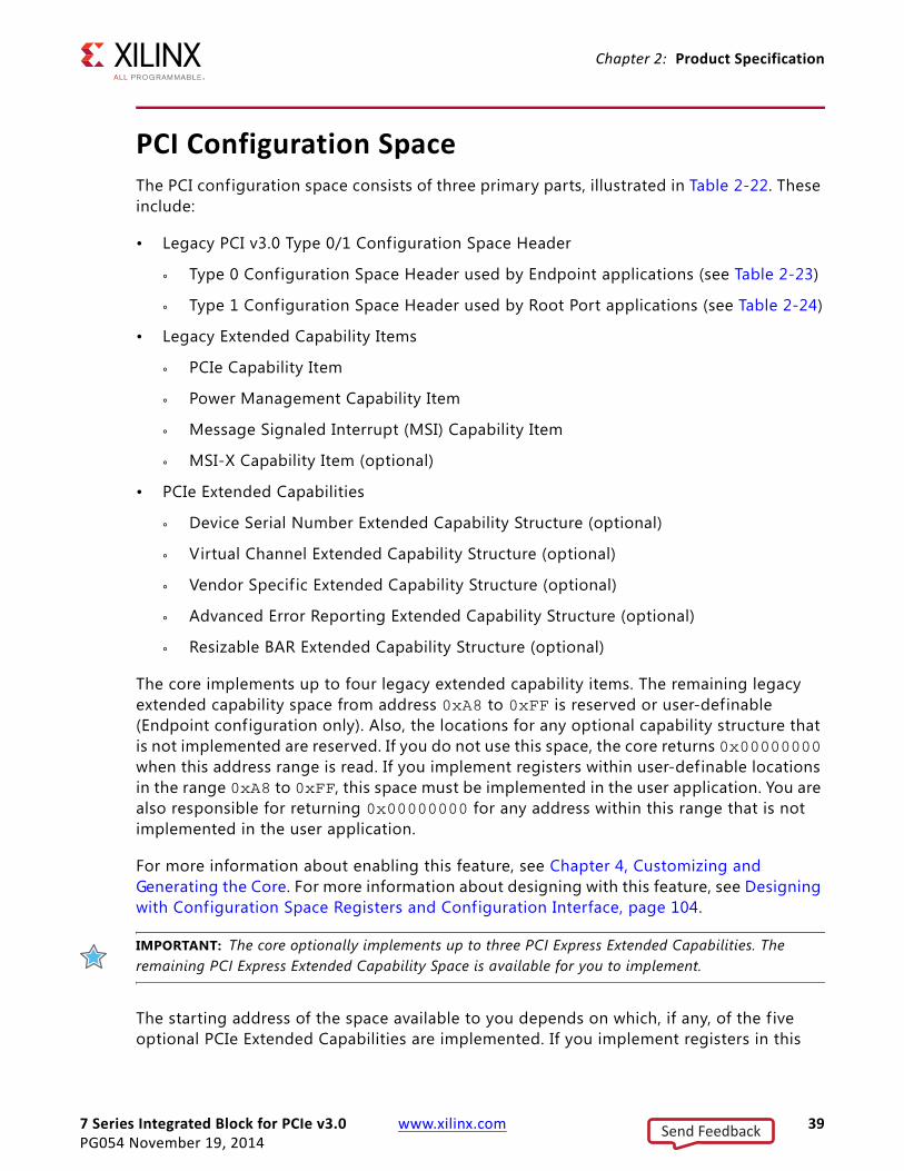
7 Series Integrated Block for PCIe v3.0 www.xilinx.com 39PG054 November 19, 2014
Chapter 2: Product Specification
PCI Configuration SpaceThe PCI configuration space consists of three primary parts, illustrated in Table 2-22. These include:
• Legacy PCI v3.0 Type 0/1 Configuration Space Header
° Type 0 Configuration Space Header used by Endpoint applications (see Table 2-23)
° Type 1 Configuration Space Header used by Root Port applications (see Table 2-24)
• Legacy Extended Capability Items
° PCIe Capability Item
° Power Management Capability Item
° Message Signaled Interrupt (MSI) Capability Item
° MSI-X Capability Item (optional)
• PCIe Extended Capabilities
° Device Serial Number Extended Capability Structure (optional)
° Virtual Channel Extended Capability Structure (optional)
° Vendor Specif ic Extended Capability Structure (optional)
° Advanced Error Reporting Extended Capability Structure (optional)
° Resizable BAR Extended Capability Structure (optional)
The core implements up to four legacy extended capability items. The remaining legacy extended capability space from address 0xA8 to 0xFF is reserved or user-definable (Endpoint configuration only). Also, the locations for any optional capability structure that is not implemented are reserved. If you do not use this space, the core returns 0x00000000 when this address range is read. If you implement registers within user-definable locations in the range 0xA8 to 0xFF, this space must be implemented in the user application. You are also responsible for returning 0x00000000 for any address within this range that is not implemented in the user application.
For more information about enabling this feature, see Chapter 4, Customizing and Generating the Core. For more information about designing with this feature, see Designing with Configuration Space Registers and Configuration Interface, page 104.
IMPORTANT: The core optionally implements up to three PCI Express Extended Capabilities. The remaining PCI Express Extended Capability Space is available for you to implement.
The starting address of the space available to you depends on which, if any, of the f ive optional PCIe Extended Capabilities are implemented. If you implement registers in this
Send Feedback

7 Series Integrated Block for PCIe v3.0 www.xilinx.com 40PG054 November 19, 2014
Chapter 2: Product Specification
space, you can select the starting location of this space, and this space must be implemented in the user application. For more information about enabling this feature, see Extended Capabilities, page 223. For more information about designing with this feature, see Designing with Configuration Space Registers and Configuration Interface in Chapter 3.
Send Feedback
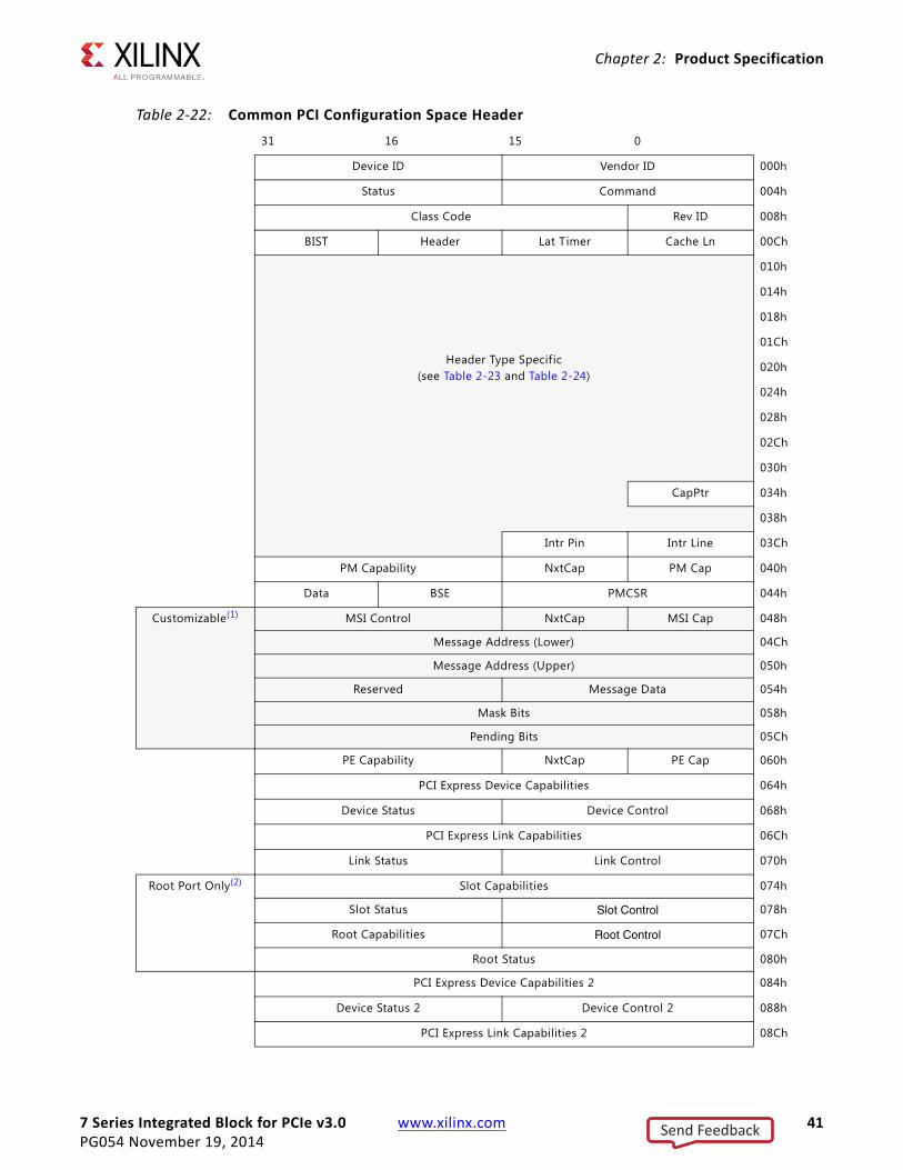
7 Series Integrated Block for PCIe v3.0 www.xilinx.com 41PG054 November 19, 2014
Chapter 2: Product Specification
Table 2-22: Common PCI Configuration Space Header31 16 15 0
Device ID Vendor ID 000h
Status Command 004h
Class Code Rev ID 008h
BIST Header Lat Timer Cache Ln 00Ch
Header Type Specific(see Table 2-23 and Table 2-24)
010h
014h
018h
01Ch
020h
024h
028h
02Ch
030h
CapPtr 034h
038h
Intr Pin Intr Line 03Ch
PM Capability NxtCap PM Cap 040h
Data BSE PMCSR 044h
Customizable(1) MSI Control NxtCap MSI Cap 048h
Message Address (Lower) 04Ch
Message Address (Upper) 050h
Reserved Message Data 054h
Mask Bits 058h
Pending Bits 05Ch
PE Capability NxtCap PE Cap 060h
PCI Express Device Capabilities 064h
Device Status Device Control 068h
PCI Express Link Capabilities 06Ch
Link Status Link Control 070h
Root Port Only(2) Slot Capabilities 074h
Slot Status Slot Control 078h
Root Capabilities Root Control 07Ch
Root Status 080h
PCI Express Device Capabilities 2 084h
Device Status 2 Device Control 2 088h
PCI Express Link Capabilities 2 08Ch
Send Feedback

7 Series Integrated Block for PCIe v3.0 www.xilinx.com 42PG054 November 19, 2014
Chapter 2: Product Specification
Link Status 2 Link Control 2 090h
Unimplemented Configuration Space (Returns 0x00000000)
094h-098h
Optional MSlx Control NxtCap MSlx Cap 09Ch
Table Offset TableBIR
0A0h
PBA Offset PBABIR
0A4h
Reserved Legacy Configuration Space (Returns 0x00000000)
0A8h-0FFh
Optional(3) Next Cap Cap.Ver.
PCI Express Extended Capability - DSN 100h
PCI Express Device Serial Number (1st) 104h
PCI Express Device Serial Number (2nd) 108h
Optional(3) Next Cap Cap.Ver.
PCI Express ExtendedCapability - VC
10Ch
Port VC Capability Register 1 110h
Port VC Capability Register 2 114h
Port VC Status Port VC Control 118h
VC Resource Capability Register 0 11Ch
VC Resource Control Register 0 120h
VC Resource Status Register 0 124h
Optional(3) Next Cap Cap.Ver.
PCI Express Extended Capability - VSEC 128h
Vendor Specific Header 12Ch
Vendor Specif ic - Loopback Command 130h
Vendor Specif ic - Loopback Status 134h
Vendor Specific - Error Count #1 138h
Vendor Specific - Error Count #2 13Ch
Optional(3)
Next Cap Cap. Ver. PCI Express Extended Cap. ID (AER) 140h
Uncorrectable Error Status Register 144h
Uncorrectable Error Mask Register 148h
Uncorrectable Error Severity Register 14Ch
Correctable Error Status Register 150h
Correctable Error Mask Register 154h
Advanced Error Cap. & Control Register 158h
Header Log Register 1 15Ch
Header Log Register 2 160h
Header Log Register 3 164h
Header Log Register 4 168h
Table 2-22: Common PCI Configuration Space Header (Cont’d)31 16 15 0
Send Feedback

7 Series Integrated Block for PCIe v3.0 www.xilinx.com 43PG054 November 19, 2014
Chapter 2: Product Specification
Optional, Root Port only(3)
Root Error Command Register 16Ch
Root Error Status Register 170h
Error Source ID Register 174h
Optional(3)
Next Cap Cap. Ver. PCI Express Extended Cap. ID (RBAR) 178h
Resizable BAR Capability Register(0) 17Ch
Reserved Resizable BAR Control(0) 180h
Resizable BAR Capability Register(1) 184h
Reserved Resizable BAR Control(1) 188h
Resizable BAR Capability Register(2) 18Ch
Reserved Resizable BAR Control(2) 190h
Resizable BAR Capability Register(3) 194h
Reserved Resizable BAR Control(3) 198h
Resizable BAR Capability Register(4) 19Ch
Reserved Resizable BAR Control(4) 1A0h
Resizable BAR Capability Register(5) 1A4h
Reserved Resizable BAR Control(5) 1A8h
Reserved Extended Configuration Space (Returns Completion with 0x00000000) 1ACh-FFFh
Notes: 1. The MSI Capability Structure varies depending on the selections in the Vivado Integrated Design Environment
(IDE).2. Reserved for Endpoint configurations (returns 0x00000000).3. The layout of the PCI Express Extended Configuration Space (100h-FFFh) can change depending on which
optional capabilities are enabled. This table represents the Extended Configuration space layout when all f ive optional extended capability structures are enabled. For more information, see Optional PCI Express Extended Capabilities, page 112.
Table 2-22: Common PCI Configuration Space Header (Cont’d)31 16 15 0
Send Feedback
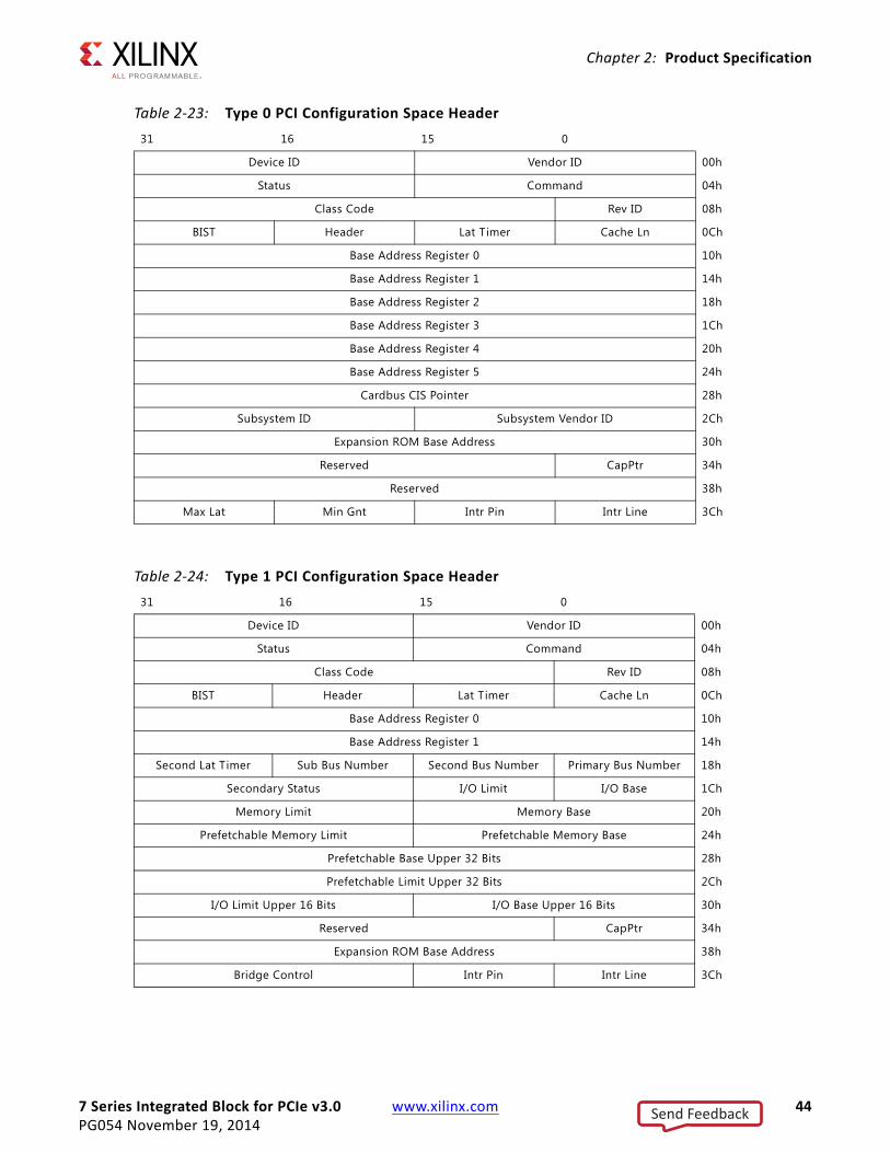
7 Series Integrated Block for PCIe v3.0 www.xilinx.com 44PG054 November 19, 2014
Chapter 2: Product Specification
Table 2-23: Type 0 PCI Configuration Space Header31 16 15 0
Device ID Vendor ID 00h
Status Command 04h
Class Code Rev ID 08h
BIST Header Lat Timer Cache Ln 0Ch
Base Address Register 0 10h
Base Address Register 1 14h
Base Address Register 2 18h
Base Address Register 3 1Ch
Base Address Register 4 20h
Base Address Register 5 24h
Cardbus CIS Pointer 28h
Subsystem ID Subsystem Vendor ID 2Ch
Expansion ROM Base Address 30h
Reserved CapPtr 34h
Reserved 38h
Max Lat Min Gnt Intr Pin Intr Line 3Ch
Table 2-24: Type 1 PCI Configuration Space Header31 16 15 0
Device ID Vendor ID 00h
Status Command 04h
Class Code Rev ID 08h
BIST Header Lat Timer Cache Ln 0Ch
Base Address Register 0 10h
Base Address Register 1 14h
Second Lat Timer Sub Bus Number Second Bus Number Primary Bus Number 18h
Secondary Status I/O Limit I/O Base 1Ch
Memory Limit Memory Base 20h
Prefetchable Memory Limit Prefetchable Memory Base 24h
Prefetchable Base Upper 32 Bits 28h
Prefetchable Limit Upper 32 Bits 2Ch
I/O Limit Upper 16 Bits I/O Base Upper 16 Bits 30h
Reserved CapPtr 34h
Expansion ROM Base Address 38h
Bridge Control Intr Pin Intr Line 3Ch
Send Feedback
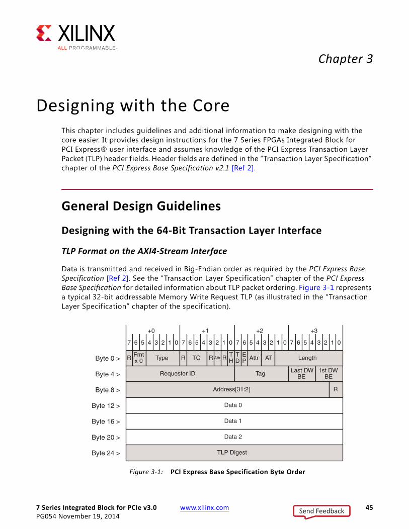
7 Series Integrated Block for PCIe v3.0 www.xilinx.com 45PG054 November 19, 2014
Chapter 3
Designing with the CoreThis chapter includes guidelines and additional information to make designing with the core easier. It provides design instructions for the 7 Series FPGAs Integrated Block for PCI Express® user interface and assumes knowledge of the PCI Express Transaction Layer Packet (TLP) header fields. Header f ields are defined in the “Transaction Layer Specification” chapter of the PCI Express Base Specification v2.1 [Ref 2].
General Design Guidelines
Designing with the 64-Bit Transaction Layer Interface
TLP Format on the AXI4-Stream Interface
Data is transmitted and received in Big-Endian order as required by the PCI Express Base Specification [Ref 2]. See the “Transaction Layer Specif ication” chapter of the PCI Express Base Specification for detailed information about TLP packet ordering. Figure 3-1 represents a typical 32-bit addressable Memory Write Request TLP (as illustrated in the “Transaction Layer Specif ication” chapter of the specification).
.X-Ref Target - Figure 3-1
Figure 3-1: PCI Express Base Specification Byte Order
+0
Byte 0 > R Fmtx 0 Type R TC T
DTH
EP AttrAttr AT Length
Byte 4 > Requester ID Tag Last DWBE
1st DWBE
Byte 8 >
Byte 12 >
Address[31:2] R
Data 0
Byte 16 >
Byte 20 >
Data 1
Data 2
Byte 24 > TLP Digest
7 6 5 4 3 2 1 0
+1
7 6 5 4 3 2 1 0
+2
7 6 5 4 3 2 1 0
+3
7 6 5 4 3 2 1 0
R R
Send Feedback
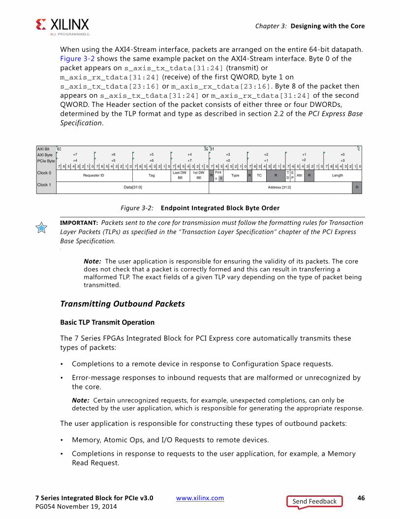
7 Series Integrated Block for PCIe v3.0 www.xilinx.com 46PG054 November 19, 2014
Chapter 3: Designing with the Core
When using the AXI4-Stream interface, packets are arranged on the entire 64-bit datapath. Figure 3-2 shows the same example packet on the AXI4-Stream interface. Byte 0 of the packet appears on s_axis_tx_tdata[31:24] (transmit) or m_axis_rx_tdata[31:24] (receive) of the first QWORD, byte 1 on s_axis_tx_tdata[23:16] or m_axis_rx_tdata[23:16]. Byte 8 of the packet then appears on s_axis_tx_tdata[31:24] or m_axis_rx_tdata[31:24] of the second QWORD. The Header section of the packet consists of either three or four DWORDs, determined by the TLP format and type as described in section 2.2 of the PCI Express Base Specification.
IMPORTANT: Packets sent to the core for transmission must follow the formatting rules for Transaction Layer Packets (TLPs) as specified in the “Transaction Layer Specification” chapter of the PCI Express Base Specification.
Note: The user application is responsible for ensuring the validity of its packets. The core does not check that a packet is correctly formed and this can result in transferring a malformed TLP. The exact f ields of a given TLP vary depending on the type of packet being transmitted.
Transmitting Outbound Packets
Basic TLP Transmit Operation
The 7 Series FPGAs Integrated Block for PCI Express core automatically transmits these types of packets:
• Completions to a remote device in response to Configuration Space requests.
• Error-message responses to inbound requests that are malformed or unrecognized by the core.
Note: Certain unrecognized requests, for example, unexpected completions, can only be detected by the user application, which is responsible for generating the appropriate response.
The user application is responsible for constructing these types of outbound packets:
• Memory, Atomic Ops, and I/O Requests to remote devices.
• Completions in response to requests to the user application, for example, a Memory Read Request.
X-Ref Target - Figure 3-2
Figure 3-2: Endpoint Integrated Block Byte Order
AXI Bit 63 32 31 0 AXI Byte
PCIe Byte7 6 5 4 3 2 1 0 7 6 5 4 3 2 1 0 7 6 5 4 3 2 1 0 7 6 5 4 3 2 1 0 7 6 5 4 3 2 1 0 7 6 5 4 3 2 1 0 7 6 5 4 3 2 1 0 7 6 5 4 3 2 1 0
Clock 0 x 0
Clock 1
+2 +1 +0 +7 +6 +5 +4 +3 +3 +4 +5 +6 +7 +0 +1
Data[31:0] Address [31:2] R
Requester ID Tag Last DW BE Length 1st DW
BE R Fmt Type R TC R T
D E P Attr R
+2
Send Feedback
7 Series Integrated Block for PCIe v3.0 www.xilinx.com 47PG054 November 19, 2014
Chapter 3: Designing with the Core
• Completions in response to user-implemented Configuration Space requests, when enabled. These requests include PCI™ legacy capability registers beyond address BFh and PCI Express extended capability registers beyond address 1FFh.
Note: For information about accessing user-implemented Configuration Space while in a low-power state, see Power Management, page 133.
When configured as an Endpoint, the core notif ies the user application of pending internally generated TLPs that arbitrate for the transmit datapath by asserting tx_cfg_req (1b). The user application can choose to give priority to core-generated TLPs by asserting tx_cfg_gnt (1b) permanently, without regard to tx_cfg_req. Doing so prevents User-Application-generated TLPs from being transmitted when a core-generated TLP is pending. Alternatively, the user application can reserve priority for a generated TLP over core-generated TLPs, by deasserting tx_cfg_gnt (0b) until the user transaction is complete. When the user transaction is complete, the user application can assert tx_cfg_gnt (1b) for at least one clock cycle to allow the pending core-generated TLP to be transmitted. You must not delay asserting tx_cfg_gnt indefinitely, because this might cause a completion timeout in the requester. See the PCI Express Base Specification [Ref 2] for more information on the Completion Timeout Mechanism.
The integrated block does not do any f iltering on the Base/Limit registers (Root Port only). You are responsible for determining if f iltering is required. These registers can be read out of the Type 1 Configuration Header space through the Configuration interface (see Designing with Configuration Space Registers and Configuration Interface, page 104).
Table 2-10, page 17 defines the transmit user application signals. To transmit a TLP, the user application must perform this sequence of events on the transmit transaction interface:
1. The user application logic asserts s_axis_tx_tvalid and presents the first TLP QWORD on s_axis_tx_tdata[63:0]. If the core is asserting s_axis_tx_tready, the QWORD is accepted immediately; otherwise, the user application must keep the QWORD presented until the core asserts s_axis_tx_tready.
2. The user application asserts s_axis_tx_tvalid and presents the remainder of the TLP QWORDs on s_axis_tx_tdata[63:0] for subsequent clock cycles (for which the core asserts s_axis_tx_tready).
3. The user application asserts s_axis_tx_tvalid and s_axis_tx_tlast together with the last QWORD data. If all eight data bytes of the last transfer are valid, they are presented on s_axis_tx_tdata[63:0] and s_axis_tx_tkeep is driven to 0xFF; otherwise, the four remaining data bytes are presented on s_axis_tx_tdata[31:0], and s_axis_tx_tkeep is driven to 0x0F.
4. At the next clock cycle, the user application deasserts s_axis_tx_tvalid to signal the end of valid transfers on s_axis_tx_tdata[63:0].
Figure 3-3 illustrates a 3-DW TLP header without a data payload; an example is a 32-bit addressable Memory Read request. When the user application asserts s_axis_tx_tlast,
Send Feedback
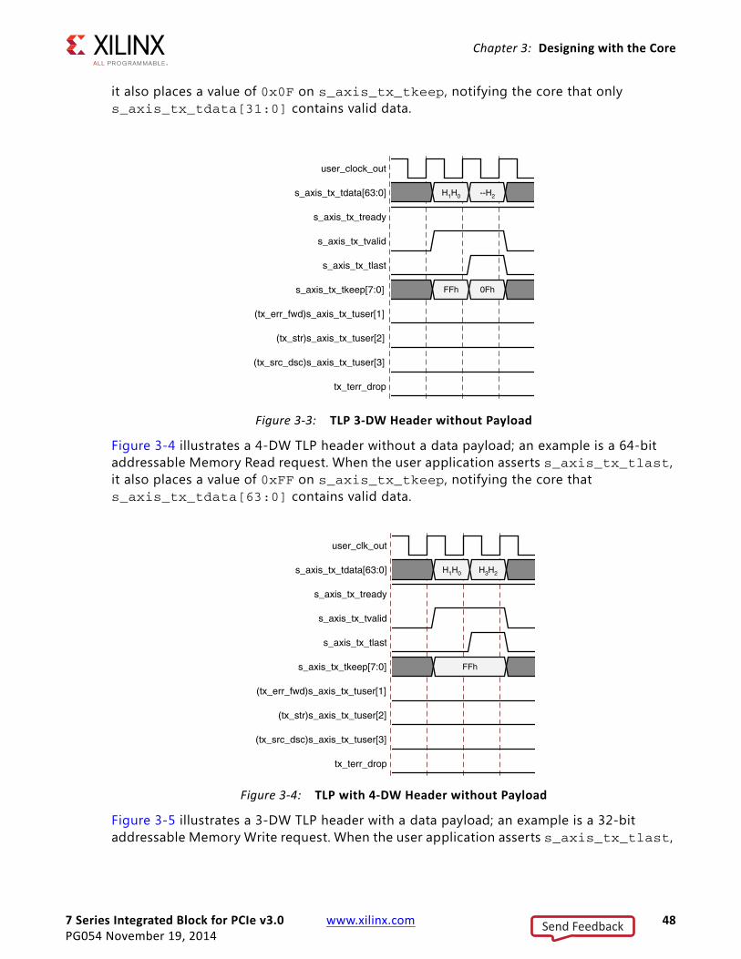
7 Series Integrated Block for PCIe v3.0 www.xilinx.com 48PG054 November 19, 2014
Chapter 3: Designing with the Core
it also places a value of 0x0F on s_axis_tx_tkeep, notifying the core that only s_axis_tx_tdata[31:0] contains valid data.
Figure 3-4 illustrates a 4-DW TLP header without a data payload; an example is a 64-bit addressable Memory Read request. When the user application asserts s_axis_tx_tlast, it also places a value of 0xFF on s_axis_tx_tkeep, notifying the core that s_axis_tx_tdata[63:0] contains valid data.
Figure 3-5 illustrates a 3-DW TLP header with a data payload; an example is a 32-bit addressable Memory Write request. When the user application asserts s_axis_tx_tlast,
X-Ref Target - Figure 3-3
Figure 3-3: TLP 3-DW Header without Payload
X-Ref Target - Figure 3-4
Figure 3-4: TLP with 4-DW Header without Payload
user_clock_out
s_axis_tx_tdata[63:0]
s_axis_tx_tready
s_axis_tx_tvalid
s_axis_tx_tlast
s_axis_tx_tkeep[7:0]
(tx_err_fwd)s_axis_tx_tuser[1]
(tx_str)s_axis_tx_tuser[2]
(tx_src_dsc)s_axis_tx_tuser[3]
tx_terr_drop
H1H0 --H2
FFh 0Fh
user_clk_out
s_axis_tx_tdata[63:0]
s_axis_tx_tready
s_axis_tx_tvalid
s_axis_tx_tlast
s_axis_tx_tkeep[7:0]
(tx_err_fwd)s_axis_tx_tuser[1]
(tx_str)s_axis_tx_tuser[2]
(tx_src_dsc)s_axis_tx_tuser[3]
tx_terr_drop
H1H0 H3H2
FFh
Send Feedback

7 Series Integrated Block for PCIe v3.0 www.xilinx.com 49PG054 November 19, 2014
Chapter 3: Designing with the Core
it also puts a value of 0xFF on s_axis_tx_tkeep, notifying the core that s_axis_tx_tdata[63:0] contains valid data.
Figure 3-6 illustrates a 4-DW TLP header with a data payload; an example is a 64-bit addressable Memory Write request. When the user application asserts s_axis_tx_tlast, it also places a value of 0x0F on s_axis_tx_tkeep, notifying the core that only s_axis_tx_tdata[31:0] contains valid data.
Presenting Back-to-Back Transactions on the Transmit Interface
The user application can present back-to-back TLPs on the transmit AXI4-Stream interface to maximize bandwidth utilization. Figure 3-7 illustrates back-to-back TLPs presented on the transmit interface. The user application keeps s_axis_tx_tvalid asserted and
X-Ref Target - Figure 3-5
Figure 3-5: TLP with 3-DW Header with Payload
X-Ref Target - Figure 3-6
Figure 3-6: TLP with 4-DW Header with Payload
user_clock_out
s_axis_tx_tdata[63:0]
s_axis_tx_tready
s_axis_tx_tvalid
s_axis_tx_tlast
s_axis_tx_tkeep[7:0]
(terr_fwd)s_axis_tx_tuser[1]
(str)s_axis_tx_tuser[2]
(src_dsc)s_axis_tx_tuser[3]
tx_terr_drop
H1H0 D0H2 D2D1 Dn-2Dn-3 DnDn-1
FFh FFh
user_clk_out
s_axis_tx_tdata[63:0]
s_axis_tx_tready
s_axis_tx_tvalid
s_axis_tx_tlast
s_axis_tx_tkeep[7:0]
(terr_fwd)s_axis_tx_tuser[1]
(str)s_axis_tx_tuser[2]
(src_dsc)s_axis_tx_tuser[3]
tx_terr_drop
H1H0 H3H2 D1D0 D3D2 Dn-1Dn-2 --Dn
FFh 0Fh
Send Feedback
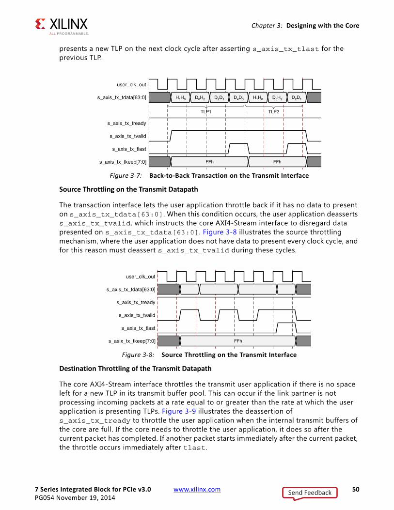
7 Series Integrated Block for PCIe v3.0 www.xilinx.com 50PG054 November 19, 2014
Chapter 3: Designing with the Core
presents a new TLP on the next clock cycle after asserting s_axis_tx_tlast for the previous TLP.
Source Throttling on the Transmit Datapath
The transaction interface lets the user application throttle back if it has no data to present on s_axis_tx_tdata[63:0]. When this condition occurs, the user application deasserts s_axis_tx_tvalid, which instructs the core AXI4-Stream interface to disregard data presented on s_axis_tx_tdata[63:0]. Figure 3-8 illustrates the source throttling mechanism, where the user application does not have data to present every clock cycle, and for this reason must deassert s_axis_tx_tvalid during these cycles.
Destination Throttling of the Transmit Datapath
The core AXI4-Stream interface throttles the transmit user application if there is no space left for a new TLP in its transmit buffer pool. This can occur if the link partner is not processing incoming packets at a rate equal to or greater than the rate at which the user application is presenting TLPs. Figure 3-9 illustrates the deassertion of s_axis_tx_tready to throttle the user application when the internal transmit buffers of the core are full. If the core needs to throttle the user application, it does so after the current packet has completed. If another packet starts immediately after the current packet, the throttle occurs immediately after tlast.
X-Ref Target - Figure 3-7
Figure 3-7: Back-to-Back Transaction on the Transmit Interface
X-Ref Target - Figure 3-8
Figure 3-8: Source Throttling on the Transmit Interface
user_clk_out
s_axis_tx_tdata[63:0]
s_axis_tx_tready
s_axis_tx_tvalid
s_axis_tx_tlast
s_axis_tx_tkeep[7:0]
H1H0 D0H2 D2D1 D4D3 H1H0 D0H2 D2D1
FFh FFh
TLP1 TLP2
user_clk_out
s_axis_tx_tdata[63:0]
s_axis_tx_tready
s_axis_tx_tvalid
s_axis_tx_tlast
s_asix_tx_tkeep[7:0] FFh
Send Feedback
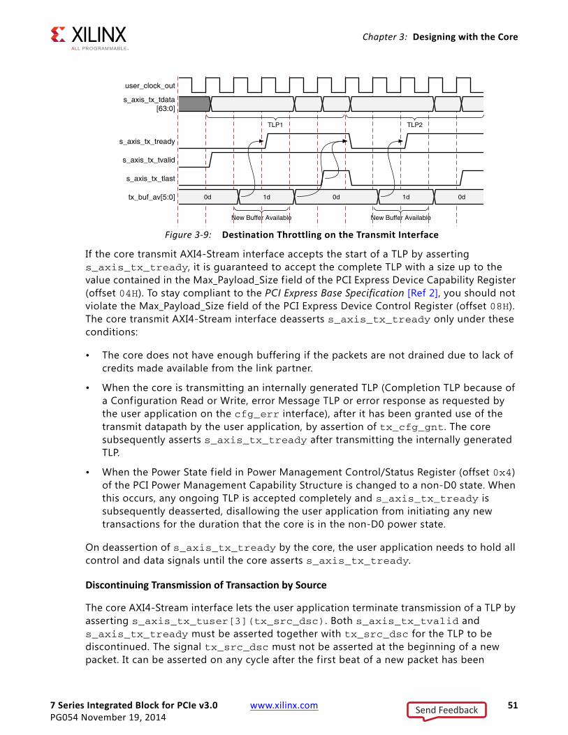
7 Series Integrated Block for PCIe v3.0 www.xilinx.com 51PG054 November 19, 2014
Chapter 3: Designing with the Core
If the core transmit AXI4-Stream interface accepts the start of a TLP by asserting s_axis_tx_tready, it is guaranteed to accept the complete TLP with a size up to the value contained in the Max_Payload_Size field of the PCI Express Device Capability Register (offset 04H). To stay compliant to the PCI Express Base Specification [Ref 2], you should not violate the Max_Payload_Size field of the PCI Express Device Control Register (offset 08H). The core transmit AXI4-Stream interface deasserts s_axis_tx_tready only under these conditions:
• The core does not have enough buffering if the packets are not drained due to lack of credits made available from the link partner.
• When the core is transmitting an internally generated TLP (Completion TLP because of a Configuration Read or Write, error Message TLP or error response as requested by the user application on the cfg_err interface), after it has been granted use of the transmit datapath by the user application, by assertion of tx_cfg_gnt. The core subsequently asserts s_axis_tx_tready after transmitting the internally generated TLP.
• When the Power State field in Power Management Control/Status Register (offset 0x4) of the PCI Power Management Capability Structure is changed to a non-D0 state. When this occurs, any ongoing TLP is accepted completely and s_axis_tx_tready is subsequently deasserted, disallowing the user application from initiating any new transactions for the duration that the core is in the non-D0 power state.
On deassertion of s_axis_tx_tready by the core, the user application needs to hold all control and data signals until the core asserts s_axis_tx_tready.
Discontinuing Transmission of Transaction by Source
The core AXI4-Stream interface lets the user application terminate transmission of a TLP by asserting s_axis_tx_tuser[3](tx_src_dsc). Both s_axis_tx_tvalid and s_axis_tx_tready must be asserted together with tx_src_dsc for the TLP to be discontinued. The signal tx_src_dsc must not be asserted at the beginning of a new packet. It can be asserted on any cycle after the first beat of a new packet has been
X-Ref Target - Figure 3-9
Figure 3-9: Destination Throttling on the Transmit Interface
user_clock_out
s_axis_tx_tdata [63:0]
s_axis_tx_tready
s_axis_tx_tvalid
s_axis_tx_tlast
tx_buf_av[5:0] 0d 1d 0d 1d 0d
TLP1 TLP2
New Buffer Available New Buffer Available
Send Feedback
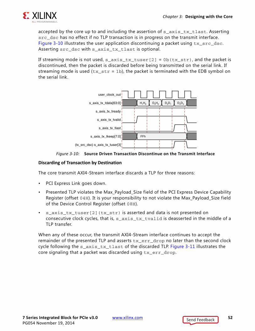
7 Series Integrated Block for PCIe v3.0 www.xilinx.com 52PG054 November 19, 2014
Chapter 3: Designing with the Core
accepted by the core up to and including the assertion of s_axis_tx_tlast. Asserting src_dsc has no effect if no TLP transaction is in progress on the transmit interface. Figure 3-10 illustrates the user application discontinuing a packet using tx_src_dsc. Asserting src_dsc with s_axis_tx_tlast is optional.
If streaming mode is not used, s_axis_tx_tuser[2] = 0b(tx_str), and the packet is discontinued, then the packet is discarded before being transmitted on the serial link. If streaming mode is used (tx_str = 1b), the packet is terminated with the EDB symbol on the serial link.
Discarding of Transaction by Destination
The core transmit AXI4-Stream interface discards a TLP for three reasons:
• PCI Express Link goes down.
• Presented TLP violates the Max_Payload_Size f ield of the PCI Express Device Capability Register (offset 04H). It is your responsibility to not violate the Max_Payload_Size field of the Device Control Register (offset 08H).
• s_axis_tx_tuser[2](tx_str) is asserted and data is not presented on consecutive clock cycles, that is, s_axis_tx_tvalid is deasserted in the middle of a TLP transfer.
When any of these occur, the transmit AXI4-Stream interface continues to accept the remainder of the presented TLP and asserts tx_err_drop no later than the second clock cycle following the s_axis_tx_tlast of the discarded TLP. Figure 3-11 illustrates the core signaling that a packet was discarded using tx_err_drop.
X-Ref Target - Figure 3-10
Figure 3-10: Source Driven Transaction Discontinue on the Transmit Interface
user_clock_out
s_axis_tx_tdata[63:0]
s_axis_tx_tready
s_axis_tx_tvalid
s_axis_tx_tlast
s_axis_tx_tkeep[7:0]
(tx_src_dsc) s_axis_tx_tuser[3]
H1H0 D0H2 D2D1 D4D3
FFh
Send Feedback
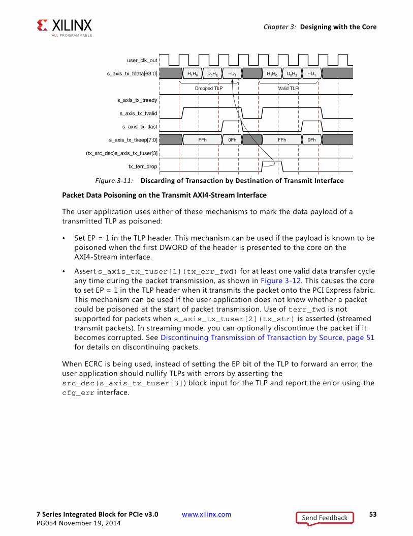
7 Series Integrated Block for PCIe v3.0 www.xilinx.com 53PG054 November 19, 2014
Chapter 3: Designing with the Core
Packet Data Poisoning on the Transmit AXI4-Stream Interface
The user application uses either of these mechanisms to mark the data payload of a transmitted TLP as poisoned:
• Set EP = 1 in the TLP header. This mechanism can be used if the payload is known to be poisoned when the f irst DWORD of the header is presented to the core on the AXI4-Stream interface.
• Assert s_axis_tx_tuser[1](tx_err_fwd) for at least one valid data transfer cycle any time during the packet transmission, as shown in Figure 3-12. This causes the core to set EP = 1 in the TLP header when it transmits the packet onto the PCI Express fabric. This mechanism can be used if the user application does not know whether a packet could be poisoned at the start of packet transmission. Use of terr_fwd is not supported for packets when s_axis_tx_tuser[2](tx_str) is asserted (streamed transmit packets). In streaming mode, you can optionally discontinue the packet if it becomes corrupted. See Discontinuing Transmission of Transaction by Source, page 51 for details on discontinuing packets.
When ECRC is being used, instead of setting the EP bit of the TLP to forward an error, the user application should nullify TLPs with errors by asserting the src_dsc(s_axis_tx_tuser[3]) block input for the TLP and report the error using the cfg_err interface.
X-Ref Target - Figure 3-11
Figure 3-11: Discarding of Transaction by Destination of Transmit Interface
user_clk_out
s_axis_tx_tdata[63:0]
s_axis_tx_tready
s_axis_tx_tvalid
s_axis_tx_tlast
s_axis_tx_tkeep[7:0]
(tx_src_dsc)s_axis_tx_tuser[3]
tx_terr_drop
H1H0 D0H2 --D1 H1H0 D0H2 --D1
FFh 0Fh FFh 0Fh
Dropped TLP Valid TLP
Send Feedback
7 Series Integrated Block for PCIe v3.0 www.xilinx.com 54PG054 November 19, 2014
Chapter 3: Designing with the Core
Streaming Mode for Transactions on the Transmit Interface
The 7 Series FPGAs Integrated Block for PCI Express core allows the user application to enable Streaming (cut-through) mode for transmission of a TLP, when possible, to reduce latency of operation. To enable this feature, the user application must hold s_axis_tx_tuser[2](tx_str) asserted for the entire duration of the transmitted TLP. The user application must also present valid frames on every clock cycle until the f inal cycle of the TLP. In other words, the user application must not deassert s_axis_tx_tvalid for the duration of the presented TLP. Source throttling of the transaction while in streaming mode of operation causes the transaction to be dropped (tx_err_drop is asserted) and a nullif ied TLP to be signaled on the PCI Express link. Figure 3-13 illustrates the streaming mode of operation, where the f irst TLP is streamed and the second TLP is dropped because of source throttling.
Using ECRC Generation
The integrated block supports automatic ECRC generation. To enable this feature, the user application must assert s_axis_tx_tuser[0](tx_ecrc_gen) at the beginning of a TLP on the transmit AXI4-Stream interface. This signal can be asserted through the duration of the packet, if desired. If the outgoing TLP does not already have a digest, the core generates and appends one and sets the TD bit. There is a single-clock cycle deassertion of
X-Ref Target - Figure 3-12
Figure 3-12: Packet Data Poisoning on the Transmit Interface
user_clk_out
s_axis_tx_tdata[63:0]
s_axis_tx_tvalid
s_axis_tx_tlast
s_axis_tx_tkeep[7:0]
(tx_err_fwd)s_axis_tx_tuser[1]
FFh FFh 0Fh
Poisoned TLP
X-Ref Target - Figure 3-13
Figure 3-13: Streaming Mode on the Transmit Interface
user_clk_out
s_axis_tx_tdata[63:0]
s_axis_tx_tready
s_axis_tx_tvalid
s_axis_tx_tlast
s_axis_tx_tkeep[7:0]
(tx_str)s_axis_tx_tuser[2]
tx_terr_drop
FFh FFh FFh
TLP1 TLP2
Send Feedback
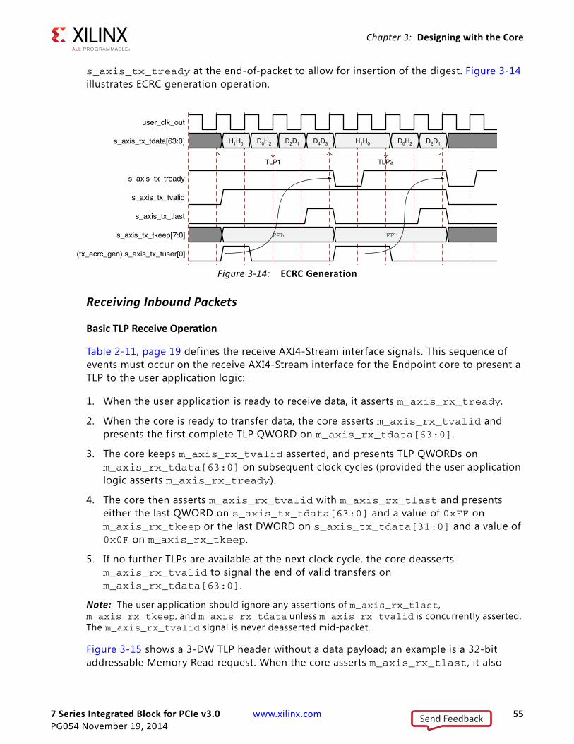
7 Series Integrated Block for PCIe v3.0 www.xilinx.com 55PG054 November 19, 2014
Chapter 3: Designing with the Core
s_axis_tx_tready at the end-of-packet to allow for insertion of the digest. Figure 3-14 illustrates ECRC generation operation.
Receiving Inbound Packets
Basic TLP Receive Operation
Table 2-11, page 19 defines the receive AXI4-Stream interface signals. This sequence of events must occur on the receive AXI4-Stream interface for the Endpoint core to present a TLP to the user application logic:
1. When the user application is ready to receive data, it asserts m_axis_rx_tready.
2. When the core is ready to transfer data, the core asserts m_axis_rx_tvalid and presents the first complete TLP QWORD on m_axis_rx_tdata[63:0].
3. The core keeps m_axis_rx_tvalid asserted, and presents TLP QWORDs on m_axis_rx_tdata[63:0] on subsequent clock cycles (provided the user application logic asserts m_axis_rx_tready).
4. The core then asserts m_axis_rx_tvalid with m_axis_rx_tlast and presents either the last QWORD on s_axis_tx_tdata[63:0] and a value of 0xFF on m_axis_rx_tkeep or the last DWORD on s_axis_tx_tdata[31:0] and a value of 0x0F on m_axis_rx_tkeep.
5. If no further TLPs are available at the next clock cycle, the core deasserts m_axis_rx_tvalid to signal the end of valid transfers on m_axis_rx_tdata[63:0].
Note: The user application should ignore any assertions of m_axis_rx_tlast, m_axis_rx_tkeep, and m_axis_rx_tdata unless m_axis_rx_tvalid is concurrently asserted. The m_axis_rx_tvalid signal is never deasserted mid-packet.
Figure 3-15 shows a 3-DW TLP header without a data payload; an example is a 32-bit addressable Memory Read request. When the core asserts m_axis_rx_tlast, it also
X-Ref Target - Figure 3-14
Figure 3-14: ECRC Generation
user_clk_out
s_axis_tx_tdata[63:0]
s_axis_tx_tready
s_axis_tx_tvalid
s_axis_tx_tlast
s_axis_tx_tkeep[7:0]
(tx_ecrc_gen) s_axis_tx_tuser[0]
H1H0 D0H2 D2D1 D4D3 H1H0 D0H2 D2D1
FFh FFh
TLP1 TLP2
Send Feedback
7 Series Integrated Block for PCIe v3.0 www.xilinx.com 56PG054 November 19, 2014
Chapter 3: Designing with the Core
places a value of 0x0F on m_axis_rx_tkeep, notifying you that only m_axis_rx_tdata[31:0] contains valid data.
Figure 3-16 shows a 4-DW TLP header without a data payload; an example is a 64-bit addressable Memory Read request. When the core asserts m_axis_rx_tlast, it also places a value of 0xFF on m_axis_rx_tkeep, notifying you that m_axis_rx_tdata[63:0] contains valid data.
Figure 3-17 shows a 3-DW TLP header with a data payload; an example is a 32-bit addressable Memory Write request. When the core asserts m_axis_rx_tlast, it also places a value of 0xFF on m_axis_rx_tkeep, notifying you that m_axis_rx_tdata[63:0] contains valid data.
X-Ref Target - Figure 3-15
Figure 3-15: TLP 3-DW Header without Payload
X-Ref Target - Figure 3-16
Figure 3-16: TLP 4-DW Header without Payload
user_clk_out
m_axis_rx_tdata[63:0]
m_axis_rx_tready
m_axis_rx_tvalid
m_axis_rx_tlast
m_axis_rx_tkeep[7:0]
(rx_err_fwd) m_axis_rx_tuser[1]
(rx_bar_hit[7:0]) m_axis_rx_tuser[9:2]
H1H0 --H3
FFh 0Fh
user_clk_out
m_axis_rx_tdata[63:0]
m_axis_rx_tready
m_axis_rx_tvalid
m_axis_rx_tlast
m_axis_rx_tkeep[7:0]
(rx_err_fwd) m_axis_rx_tuser[1]
(rx_bar_hit[7:0]) m_axis_rx_tuser[9:2]
H1H0 H3H2
FFh
Send Feedback
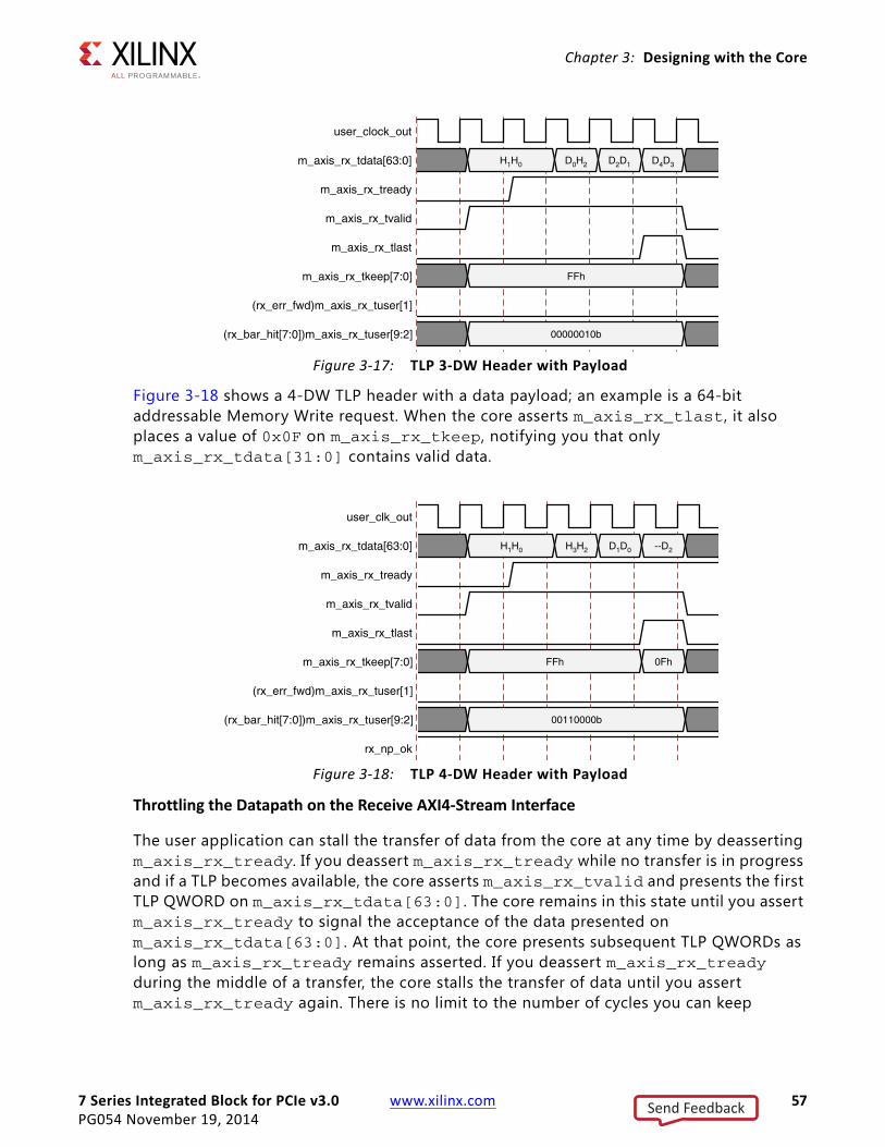
7 Series Integrated Block for PCIe v3.0 www.xilinx.com 57PG054 November 19, 2014
Chapter 3: Designing with the Core
Figure 3-18 shows a 4-DW TLP header with a data payload; an example is a 64-bit addressable Memory Write request. When the core asserts m_axis_rx_tlast, it also places a value of 0x0F on m_axis_rx_tkeep, notifying you that only m_axis_rx_tdata[31:0] contains valid data.
Throttling the Datapath on the Receive AXI4-Stream Interface
The user application can stall the transfer of data from the core at any time by deasserting m_axis_rx_tready. If you deassert m_axis_rx_tready while no transfer is in progress and if a TLP becomes available, the core asserts m_axis_rx_tvalid and presents the first TLP QWORD on m_axis_rx_tdata[63:0]. The core remains in this state until you assert m_axis_rx_tready to signal the acceptance of the data presented on m_axis_rx_tdata[63:0]. At that point, the core presents subsequent TLP QWORDs as long as m_axis_rx_tready remains asserted. If you deassert m_axis_rx_tready during the middle of a transfer, the core stalls the transfer of data until you assert m_axis_rx_tready again. There is no limit to the number of cycles you can keep
X-Ref Target - Figure 3-17
Figure 3-17: TLP 3-DW Header with Payload
X-Ref Target - Figure 3-18
Figure 3-18: TLP 4-DW Header with Payload
user_clock_out
m_axis_rx_tdata[63:0]
m_axis_rx_tready
m_axis_rx_tvalid
m_axis_rx_tlast
m_axis_rx_tkeep[7:0]
(rx_err_fwd)m_axis_rx_tuser[1]
(rx_bar_hit[7:0])m_axis_rx_tuser[9:2]
H1H0 D0H2 D2D1 D4D3
FFh
00000010b
user_clk_out
m_axis_rx_tdata[63:0]
m_axis_rx_tready
m_axis_rx_tvalid
m_axis_rx_tlast
m_axis_rx_tkeep[7:0]
(rx_err_fwd)m_axis_rx_tuser[1]
(rx_bar_hit[7:0])m_axis_rx_tuser[9:2]
rx_np_ok
H1H0 H3H2 D1D0 --D2
FFh 0Fh
00110000b
Send Feedback
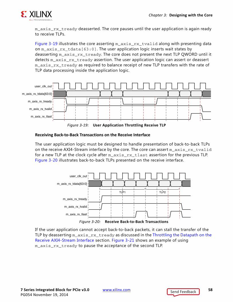
7 Series Integrated Block for PCIe v3.0 www.xilinx.com 58PG054 November 19, 2014
Chapter 3: Designing with the Core
m_axis_rx_tready deasserted. The core pauses until the user application is again ready to receive TLPs.
Figure 3-19 illustrates the core asserting m_axis_rx_tvalid along with presenting data on m_axis_rx_tdata[63:0]. The user application logic inserts wait states by deasserting m_axis_rx_tready. The core does not present the next TLP QWORD until it detects m_axis_rx_tready assertion. The user application logic can assert or deassert m_axis_rx_tready as required to balance receipt of new TLP transfers with the rate of TLP data processing inside the application logic.
Receiving Back-to-Back Transactions on the Receive Interface
The user application logic must be designed to handle presentation of back-to-back TLPs on the receive AXI4-Stream interface by the core. The core can assert m_axis_rx_tvalid for a new TLP at the clock cycle after m_axis_rx_tlast assertion for the previous TLP. Figure 3-20 illustrates back-to-back TLPs presented on the receive interface.
If the user application cannot accept back-to-back packets, it can stall the transfer of the TLP by deasserting m_axis_rx_tready as discussed in the Throttling the Datapath on the Receive AXI4-Stream Interface section. Figure 3-21 shows an example of using m_axis_rx_tready to pause the acceptance of the second TLP.
X-Ref Target - Figure 3-19
Figure 3-19: User Application Throttling Receive TLP
user_clk_out
m_axis_rx_tdata[63:0]
m_axis_rx_tready
m_axis_rx_tvalid
m_axis_rx_tlast
X-Ref Target - Figure 3-20
Figure 3-20: Receive Back-to-Back Transactions
user_clk_out
m_axis_rx_tdata[63:0]
m_axis_rx_tready
m_axis_rx_tvalid
m_axis_rx_tlast
TLP1 TLP2
Send Feedback

7 Series Integrated Block for PCIe v3.0 www.xilinx.com 59PG054 November 19, 2014
Chapter 3: Designing with the Core
Packet Re-ordering on Receive Interface
Transaction processing in the core receiver is fully compliant with the PCI transaction ordering rules, described in Chapter 2 of the PCI Express Base Specification [Ref 2]. The transaction ordering rules allow Posted and Completion TLPs to bypass blocked Non-Posted TLPs.
The core provides two mechanisms for user applications to manage their Receiver Non-Posted Buffer space.
1. Receive Non-Posted Throttling: The use of rx_np_ok to prevent the core from presenting more than two Non-Posted requests after deassertion of the rx_np_ok signal. The second mechanism,
2. Receive Request for Non-Posted: Allows user-controlled Flow Control of the Non-Posted queue, using the rx_np_req signal.
The Receive Non-Posted Throttling mechanism assumes that the user application normally has space in its receiver for non-Posted TLPs and the user application would throttle the core specif ically for Non-Posted requests. The Receive Request for Non-Posted mechanism assumes that the user application requests the core to present a Non-Posted TLP when it has space in its receiver. The two mechanisms are mutually exclusive, and only one can be active for a design. This option must be selected while generating and customizing the core. When the Receive Non-Posted Request option is selected in the Advanced Settings, the Receive Request for Non-Posted mechanism is enabled and any assertion/deassertion of rx_np_ok is ignored and vice-versa. The two mechanisms are described in further detail in the next subsections.
• Receive Non-Posted Throttling (Receive Non-Posted Request Disabled, TRN_ NP_ FC attribute FALSE)
If the user application can receive Posted and Completion Transactions from the core, but is not ready to accept Non-Posted Transactions, the user application can deassert rx_np_ok , as shown in Figure 3-22. The user application must deassert rx_np_ok at least two clock cycles before m_axis_rx_tlast of the second-to-last Non-Posted TLP
X-Ref Target - Figure 3-21
Figure 3-21: User Application Throttling Back-to-Back TLPs
user_clk_out
m_axis_rx_tdata[63:0]
m_axis_rx_tready
m_axis_rx_tvalid
m_axis_rx_tlast
m_axis_rx_tkeep[7:0] FFh 0Fh
TLP1 TLP2
Send Feedback
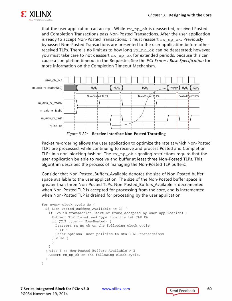
7 Series Integrated Block for PCIe v3.0 www.xilinx.com 60PG054 November 19, 2014
Chapter 3: Designing with the Core
that the user application can accept. While rx_np_ok is deasserted, received Posted and Completion Transactions pass Non-Posted Transactions. After the user application is ready to accept Non-Posted Transactions, it must reassert rx_np_ok . Previously bypassed Non-Posted Transactions are presented to the user application before other received TLPs. There is no limit as to how long rx_np_ok can be deasserted; however, you must take care to not deassert rx_np_ok for extended periods, because this can cause a completion timeout in the Requester. See the PCI Express Base Specification for more information on the Completion Timeout Mechanism.
Packet re-ordering allows the user application to optimize the rate at which Non-Posted TLPs are processed, while continuing to receive and process Posted and Completion TLPs in a non-blocking fashion. The rx_np_ok signaling restrictions require that the user application be able to receive and buffer at least three Non-Posted TLPs. This algorithm describes the process of managing the Non-Posted TLP buffers:
Consider that Non-Posted_Buffers_Available denotes the size of Non-Posted buffer space available to the user application. The size of the Non-Posted buffer space is greater than three Non-Posted TLPs. Non-Posted_Buffers_Available is decremented when Non-Posted TLP is accepted for processing from the core, and is incremented when Non-Posted TLP is drained for processing by the user application.
For every clock cycle do {if (Non-Posted_Buffers_Available <= 3) {if (Valid transaction Start-of-Frame accepted by user application) {Extract TLP Format and Type from the 1st TLP DWif (TLP type == Non-Posted) {Deassert rx_np_ok on the following clock cycle- or -Other optional user policies to stall NP transactions
} else {}
}} else { // Non-Posted_Buffers_Available > 3Assert rx_np_ok on the following clock cycle.
}}
X-Ref Target - Figure 3-22
Figure 3-22: Receive Interface Non-Posted Throttling
user_clk_out
m_axis_rx_tdata[63:0]
m_axis_rx_tready
m_axis_rx_tvalid
m_axis_rx_tlast
rx_np_ok
H1H0 H3H2 H1H0 H3H2 H1H0 D0H2
Non-Posted TLP1 Non-Posted TLP2 Posted/Cpl TLP3
Send Feedback
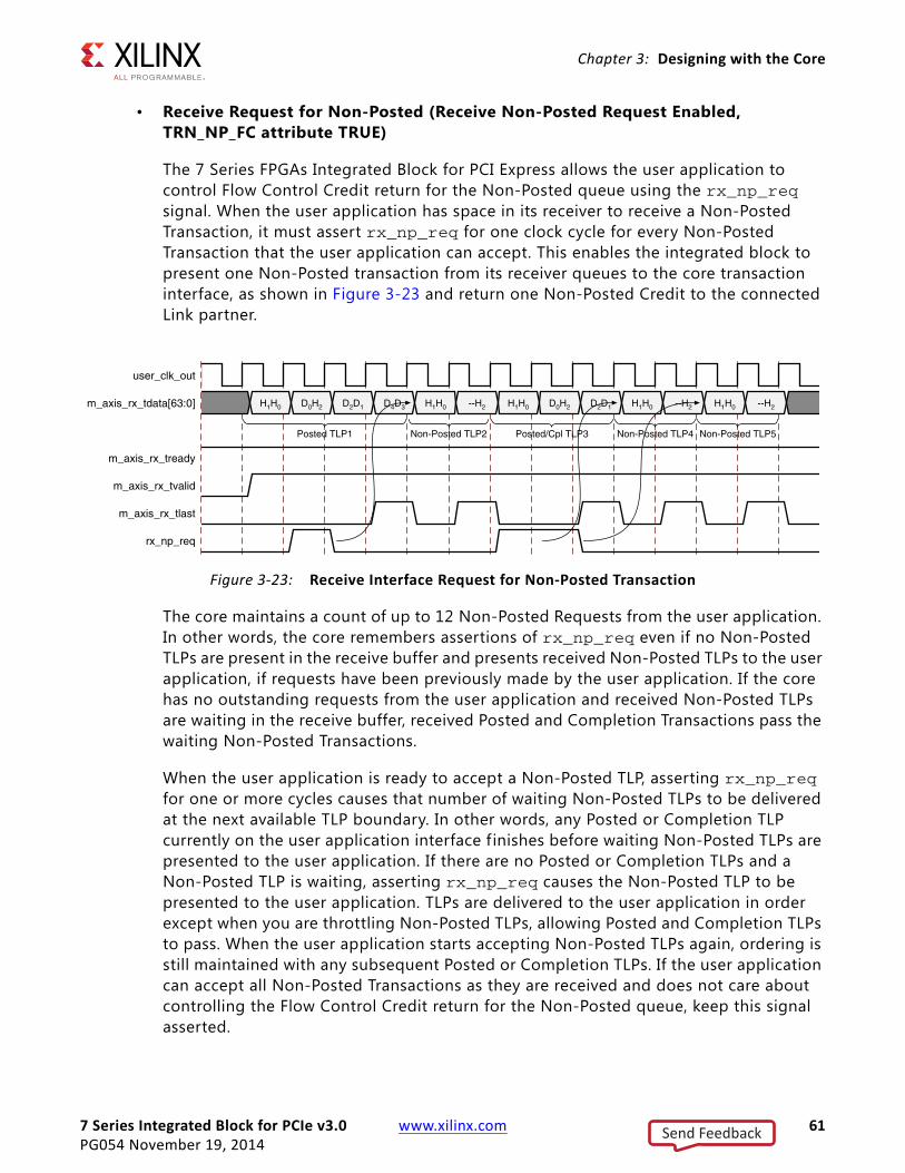
7 Series Integrated Block for PCIe v3.0 www.xilinx.com 61PG054 November 19, 2014
Chapter 3: Designing with the Core
• Receive Request for Non-Posted (Receive Non-Posted Request Enabled, TRN_ NP_ FC attribute TRUE)
The 7 Series FPGAs Integrated Block for PCI Express allows the user application to control Flow Control Credit return for the Non-Posted queue using the rx_np_req signal. When the user application has space in its receiver to receive a Non-Posted Transaction, it must assert rx_np_req for one clock cycle for every Non-Posted Transaction that the user application can accept. This enables the integrated block to present one Non-Posted transaction from its receiver queues to the core transaction interface, as shown in Figure 3-23 and return one Non-Posted Credit to the connected Link partner.
The core maintains a count of up to 12 Non-Posted Requests from the user application. In other words, the core remembers assertions of rx_np_req even if no Non-Posted TLPs are present in the receive buffer and presents received Non-Posted TLPs to the user application, if requests have been previously made by the user application. If the core has no outstanding requests from the user application and received Non-Posted TLPs are waiting in the receive buffer, received Posted and Completion Transactions pass the waiting Non-Posted Transactions.
When the user application is ready to accept a Non-Posted TLP, asserting rx_np_req for one or more cycles causes that number of waiting Non-Posted TLPs to be delivered at the next available TLP boundary. In other words, any Posted or Completion TLP currently on the user application interface f inishes before waiting Non-Posted TLPs are presented to the user application. If there are no Posted or Completion TLPs and a Non-Posted TLP is waiting, asserting rx_np_req causes the Non-Posted TLP to be presented to the user application. TLPs are delivered to the user application in order except when you are throttling Non-Posted TLPs, allowing Posted and Completion TLPs to pass. When the user application starts accepting Non-Posted TLPs again, ordering is still maintained with any subsequent Posted or Completion TLPs. If the user application can accept all Non-Posted Transactions as they are received and does not care about controlling the Flow Control Credit return for the Non-Posted queue, keep this signal asserted.
X-Ref Target - Figure 3-23
Figure 3-23: Receive Interface Request for Non-Posted Transaction
user_clk_out
m_axis_rx_tdata[63:0]
m_axis_rx_tready
m_axis_rx_tvalid
m_axis_rx_tlast
rx_np_req
H1H0 D0H2 D2D1 D4D3 H1H0 --H2 H1H0 D0H2 D2D1 H1H0 --H2 H1H0 --H2
Posted TLP1 Non-Posted TLP2 Posted/Cpl TLP3 Non-Posted TLP4 Non-Posted TLP5
Send Feedback
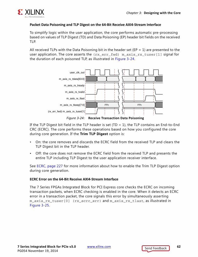
7 Series Integrated Block for PCIe v3.0 www.xilinx.com 62PG054 November 19, 2014
Chapter 3: Designing with the Core
Packet Data Poisoning and TLP Digest on the 64-Bit Receive AXI4-Stream Interface
To simplify logic within the user application, the core performs automatic pre-processing based on values of TLP Digest (TD) and Data Poisoning (EP) header bit f ields on the received TLP.
All received TLPs with the Data Poisoning bit in the header set (EP = 1) are presented to the user application. The core asserts the (rx_err_fwd) m_axis_rx_tuser[1] signal for the duration of each poisoned TLP, as illustrated in Figure 3-24.
If the TLP Digest bit f ield in the TLP header is set (TD = 1), the TLP contains an End-to-End CRC (ECRC). The core performs these operations based on how you configured the core during core generation. If the Trim TLP Digest option is:
• On: the core removes and discards the ECRC field from the received TLP and clears the TLP Digest bit in the TLP header.
• Off: the core does not remove the ECRC field from the received TLP and presents the entire TLP including TLP Digest to the user application receiver interface.
See ECRC, page 227 for more information about how to enable the Trim TLP Digest option during core generation.
ECRC Error on the 64-Bit Receive AXI4-Stream Interface
The 7 Series FPGAs Integrated Block for PCI Express core checks the ECRC on incoming transaction packets, when ECRC checking is enabled in the core. When it detects an ECRC error in a transaction packet, the core signals this error by simultaneously asserting m_axis_rx_tuser[0] (rx_ecrc_err) and m_axis_rx_tlast, as illustrated in Figure 3-25.
X-Ref Target - Figure 3-24
Figure 3-24: Receive Transaction Data Poisoning
user_clk_out
m_axis_rx_tdata[63:0]
m_axis_rx_tready
m_axis_rx_tvalid
m_axis_rx_tlast
m_axis_rx_tkeep[7:0]
(rx_err_fwd) m_axis_rx_tuser[1]
FFh FFh
Send Feedback

7 Series Integrated Block for PCIe v3.0 www.xilinx.com 63PG054 November 19, 2014
Chapter 3: Designing with the Core
Packet Base Address Register Hit on the Receive AXI4-Stream Interface
The 7 Series FPGAs Integrated Block for PCI Express in Root Port configuration does not perform any BAR decoding/filtering.
In Endpoint configuration, the core decodes incoming Memory and I/O TLP request addresses to determine which Base Address Register (BAR) in the core Type0 configuration space is being targeted, and indicates the decoded base address on m_axis_rx_tuser[9:2](rx_bar_hit[7:0]). For each received Memory or I/O TLP, a minimum of one bit and a maximum of two (adjacent) bits are set to 1b. If the received TLP targets a 32-bit Memory or I/O BAR, only one bit is asserted. If the received TLP targets a 64-bit Memory BAR, two adjacent bits are asserted. If the core receives a TLP that is not decoded by one of the BARs (that is, a misdirected TLP), then the core drops it without notif ication and it automatically generates an Unsupported Request message. Even if the core is configured for a 64-bit BAR, the system might not always allocate a 64-bit address, in which case only onerxbar_hit[7:0] signal is asserted. Overlapping BAR apertures are not allowed.
Table 3-1 illustrates mapping between rx_bar_hit[7:0] and the BARs, and the corresponding byte offsets in the core Type0 configuration header.
X-Ref Target - Figure 3-25
Figure 3-25: ECRC Error on 64-Bit Receive AXI4-Stream Interface
Table 3-1: Base Address Register Mapping
rx_bar_hit[x] m_axis_rx_tuser[x] BAR Byte Offset
0 2 0 10h
1 3 1 14h
2 4 2 18h
3 5 3 1Ch
4 6 4 20h
5 7 5 24h
6 8 Expansion ROM BAR 30h
7 9 Reserved –
user_clk_out
m_axis_rx_tdata[63:0]
m_axis_rx_tready
m_axis_rx_tvalid
m_axis_rx_tlast
m_axis_rx_tkeep[7:0]
(rx_ecrc_err) m_axis_rx_tuser[0]
FFh FFh
Send Feedback

7 Series Integrated Block for PCIe v3.0 www.xilinx.com 64PG054 November 19, 2014
Chapter 3: Designing with the Core
For a Memory or I/O TLP Transaction on the receive interface, (rx_bar_hit[7:0]) m_axis_rx_tuser[9:2] is valid for the entire TLP, starting with the assertion of m_axis_rx_tvalid, as shown in Figure 3-26. When receiving non-Memory and non-I/O transactions, signal rx_bar_hit[7:0] is undefined.
The (rx_bar_hit[7:0]) m_axis_rx_tuser[9:2] signal enables received Memory and I/O transactions to be directed to the appropriate destination apertures within the user application. By utilizing rx_bar_hit[7:0], application logic can inspect only the lower order Memory and I/O address bits within the address aperture to simplify decoding logic.
Packet Transfer During Link-Down Event on Receive AXI4-Stream Interface
The loss of communication with the link partner is signaled by deassertion of user_lnk_up. When user_lnk_up is deasserted, it effectively acts as a Hot Reset to the entire core. For this reason, all TLPs stored inside the core or being presented to the receive interface are irrecoverably lost. A TLP in progress on the Receive AXI4-Stream interface is presented to its correct length, according to the Length field in the TLP header. However, the TLP is corrupt and should be discarded by the user application. Figure 3-27 illustrates the packet transfer discontinue scenario.
X-Ref Target - Figure 3-26
Figure 3-26: BAR Target Determination Using rx_bar_hit
X-Ref Target - Figure 3-27
Figure 3-27: Receive Transaction Discontinue
user_clk_out
m_axis_rx_tdata[63:0]
m_axis_rx_tready
m_axis_rx_tvalid
m_axis_rx_tlast
(rx_bar_hit[7:0])m_axis_rx_tuser[9:2] 0000010b 0001100b
TLP1 TLP2
user_clk_out
user_lnk_up
m_axis_rx_tdata[63:0]
m_axis_rx_tready
m_axis_rx_tvalid
m_axis_rx_tlast
H1H0 D0H2 D2D1 PAD PAD
original TLP data was lost
Send Feedback

7 Series Integrated Block for PCIe v3.0 www.xilinx.com 65PG054 November 19, 2014
Chapter 3: Designing with the Core
Designing with the 128-Bit Transaction Layer InterfaceNote: The transaction interface width and frequency never change with a lane width/speed upconfigure or downconfigure.
TLP Format in the AXI4-Stream Interface
Data is transmitted and received in Big-Endian order as required by the PCI Express Base Specification [Ref 2]. See Chapter 2 of the PCI Express Base Specification for detailed information about TLP packet ordering. Figure 3-28 represents a typical 32-bit addressable Memory Write Request TLP (as illustrated in Chapter 2 of the specification).
When using the transaction interface, packets are arranged on the entire 128-bit datapath. Figure 3-29 shows the same example packet on the AXI4-Stream interface. PCIe Byte 0 of the packet appears on s_axis_tx_tdata[31:24] (transmit) or m_axis_rx_tdata[31:24] (receive) of the first DWORD, byte 1 on s_axis_tx_tdata[23:16] or m_axis_rx_tdata[23:16]. The Header section of the packet consists of either three or four DWORDs, determined by the TLP format and type as described in section 2.2 of the PCI Express Base Specification.
X-Ref Target - Figure 3-28
Figure 3-28: PCI Express Base Specification Byte Order
+0
Byte 0 > R Fmtx 0 Type R TC Rsvd T
DEP Attr R Length
Byte 4 > Requester ID Tag Last DWBE
1st DWBE
Byte 8 >
Byte 12 >
Address[31:2] R
Data 0
Byte 16 >
Byte 20 >
Data 1
Data 2
Byte 24 > TLP Digest
7 6 5 4 3 2 1 0
+1
7 6 5 4 3 2 1 0
+2
7 6 5 4 3 2 1 0
+3
7 6 5 4 3 2 1 0
X-Ref Target - Figure 3-29
Figure 3-29: Endpoint Integrated Block Byte Order
Clock 0
Clock1
Data DW 0
TLP Digest Data DW2
[127:96] [95:64] [63:32] [31:0]
Data DW 1
Header DW 2 Header DW 1 Header DW 0
PCIe Byte
AXI ByteAXI Bit
+12 +13 +14 +15 +8 +9 +10 +11 +4 +5 +6 +7 +0 +1 +2 +3
+15 +14 +13 +12 +11 +10 +9 +8 +7 +6 +5 +4 +3 +2 +1 +0
Send Feedback
7 Series Integrated Block for PCIe v3.0 www.xilinx.com 66PG054 November 19, 2014
Chapter 3: Designing with the Core
IMPORTANT: Packets sent to the core for transmission must follow the formatting rules for Transaction Layer Packets (TLPs) as specified in Chapter 2 of the PCI Express Base Specification.
The user application is responsible for ensuring the validity of the packets. The core does not check that a packet is correctly formed and this can result in transferring a malformed TLP. The exact f ields of a given TLP vary depending on the type of packet being transmitted.
Transmitting Outbound Packets
Basic TLP Transmit Operation
The 7 Series FPGAs Integrated Block for PCI Express core automatically transmits these types of packets:
• Completions to a remote device in response to Configuration Space requests.
• Error-message responses to inbound requests that are malformed or unrecognized by the core.
Note: Certain unrecognized requests, for example, unexpected completions, can only be detected by the user application, which is responsible for generating the appropriate response.
The user application is responsible for constructing these types of outbound packets:
• Memory, Atomic Ops, and I/O Requests to remote devices.
• Completions in response to requests to the user application, for example, a Memory Read Request.
When configured as an Endpoint, the core notif ies the user application of pending internally generated TLPs that arbitrate for the transmit datapath by asserting tx_cfg_req (1b). The user application can choose to give priority to core-generated TLPs by asserting tx_cfg_gnt (1b) permanently, without regard to tx_cfg_req. Doing so prevents User-Application-generated TLPs from being transmitted when a core-generated TLP is pending. Alternatively, the user application can reserve priority for a user application-generated TLP over core-generated TLPs, by deasserting tx_cfg_gnt (0b) until the transaction is complete. After the transaction is complete, the user application can assert tx_cfg_gnt (1b) for at least one clock cycle to allow the pending core-generated TLP to be transmitted. You must not delay asserting tx_cfg_gnt indefinitely, because this might cause a completion timeout in the Requester. See the PCI Express Base Specification for more information on the Completion Timeout Mechanism.
• The integrated block does not do any filtering on the Base/Limit registers (Root Port only). You are responsible for determining if f iltering is required. These registers can be read out of the Type 1 Configuration Header space through the Configuration interface (see Designing with Configuration Space Registers and Configuration Interface, page 104).
Send Feedback
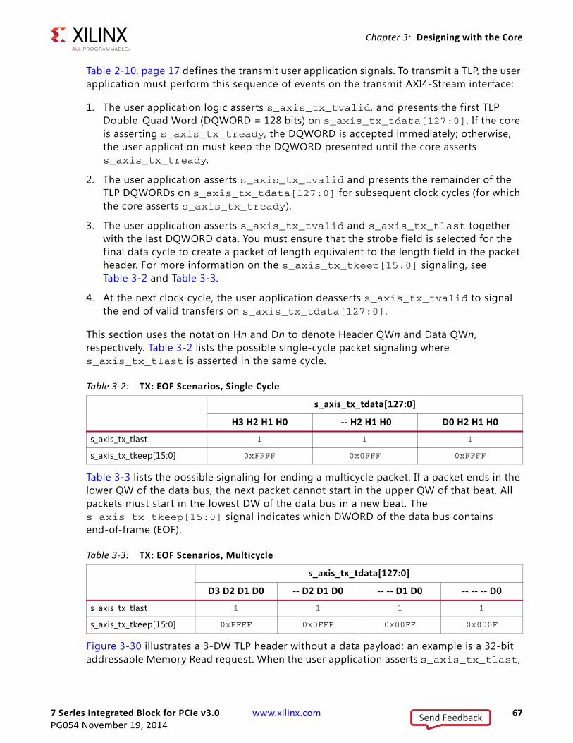
7 Series Integrated Block for PCIe v3.0 www.xilinx.com 67PG054 November 19, 2014
Chapter 3: Designing with the Core
Table 2-10, page 17 defines the transmit user application signals. To transmit a TLP, the user application must perform this sequence of events on the transmit AXI4-Stream interface:
1. The user application logic asserts s_axis_tx_tvalid, and presents the first TLP Double-Quad Word (DQWORD = 128 bits) on s_axis_tx_tdata[127:0]. If the core is asserting s_axis_tx_tready, the DQWORD is accepted immediately; otherwise, the user application must keep the DQWORD presented until the core asserts s_axis_tx_tready.
2. The user application asserts s_axis_tx_tvalid and presents the remainder of the TLP DQWORDs on s_axis_tx_tdata[127:0] for subsequent clock cycles (for which the core asserts s_axis_tx_tready).
3. The user application asserts s_axis_tx_tvalid and s_axis_tx_tlast together with the last DQWORD data. You must ensure that the strobe f ield is selected for the f inal data cycle to create a packet of length equivalent to the length f ield in the packet header. For more information on the s_axis_tx_tkeep[15:0] signaling, see Table 3-2 and Table 3-3.
4. At the next clock cycle, the user application deasserts s_axis_tx_tvalid to signal the end of valid transfers on s_axis_tx_tdata[127:0].
This section uses the notation Hn and Dn to denote Header QWn and Data QWn, respectively. Table 3-2 lists the possible single-cycle packet signaling where s_axis_tx_tlast is asserted in the same cycle.
Table 3-3 lists the possible signaling for ending a multicycle packet. If a packet ends in the lower QW of the data bus, the next packet cannot start in the upper QW of that beat. All packets must start in the lowest DW of the data bus in a new beat. The s_axis_tx_tkeep[15:0] signal indicates which DWORD of the data bus contains end-of-frame (EOF).
Figure 3-30 illustrates a 3-DW TLP header without a data payload; an example is a 32-bit addressable Memory Read request. When the user application asserts s_axis_tx_tlast,
Table 3-2: TX: EOF Scenarios, Single Cycle
s_axis_tx_tdata[127:0]
H3 H2 H1 H0 -- H2 H1 H0 D0 H2 H1 H0
s_axis_tx_tlast 1 1 1
s_axis_tx_tkeep[15:0] 0xFFFF 0x0FFF 0xFFFF
Table 3-3: TX: EOF Scenarios, Multicycle
s_axis_tx_tdata[127:0]
D3 D2 D1 D0 -- D2 D1 D0 -- -- D1 D0 -- -- -- D0
s_axis_tx_tlast 1 1 1 1
s_axis_tx_tkeep[15:0] 0xFFFF 0x0FFF 0x00FF 0x000F
Send Feedback

7 Series Integrated Block for PCIe v3.0 www.xilinx.com 68PG054 November 19, 2014
Chapter 3: Designing with the Core
it also places a value of 0x0FFF on s_axis_tx_tkeep[15:0], notifying the core that only s_axis_tx_tdata[95:0] contains valid data.
Figure 3-31 illustrates a 4-DW TLP header without a data payload; an example is a 64-bit addressable Memory Read request. When the user application asserts s_axis_tx_tlast, it also places a value of 0xFFFF on s_axis_tx_tkeep[15:0] notifying the core that s_axis_tx_tdata[127:0] contains valid data and the EOF occurs in the upper-most DW.
Figure 3-32 illustrates a 3-DW TLP header with a data payload; an example is a 32-bit addressable Memory Write request. When the user application asserts s_axis_tx_tlast, it also puts a value of 0x0FFF on s_axis_tx_tkeep[15:0] notifying the core that s_axis_tx_tdata[95:0] contains valid data and the EOF occurs in DWORD 2.
X-Ref Target - Figure 3-30
Figure 3-30: TLP 3-DW Header without Payload
X-Ref Target - Figure 3-31
Figure 3-31: TLP with 4-DW Header without Payload
user_clock_out
s_axis_tx_tdata[127:0]
s_axis_tx_tready
s_axis_tx_tvalid
s_axis_tx_tlast
s_axis_tx_tkeep[15:0]
(tx_err_fwd) s_axis_tx_tuser[1]
(tx_str) s_axis_tx_tuser[2]
(tx_src_dsc) s_axis_tx_tuser[3]
tx_terr_drop
--H2H1H0
0FFFh
user_clock_out
s_axis_tx_tdata[127:0]
s_axis_tx_tready
s_axis_tx_tvalid
s_axis_tx_tlast
s_axis_tx_tkeep[15:0]
(tx_err_fwd) s_axis_tx_tuser[1]
(tx_str) s_axis_tx_tuser[2]
(tx_src_dsc) s_axis_tx_tuser[3]
H3H2H1H0
FFFFh
Send Feedback

7 Series Integrated Block for PCIe v3.0 www.xilinx.com 69PG054 November 19, 2014
Chapter 3: Designing with the Core
Figure 3-33 illustrates a 4-DW TLP header with a data payload. When the user application asserts s_axis_tx_tlast, it also places a value of 0x00FF on s_axis_tx_tkeep[15:0], notifying the core that only s_axis_tx_tdata[63:0] contains valid data.
Presenting Back-to-Back Transactions on the Transmit Interface
The user application can present back-to-back TLPs on the transmit AXI4-Stream interface to maximize bandwidth utilization. Figure 3-34 illustrates back-to-back TLPs presented on the transmit interface, with the restriction that all TLPs must start in the lowest DW of the data bus [31:0]. The user application keeps s_axis_tx_tvalid asserted and presents a new TLP on the next clock cycle after asserting s_axis_tx_tlast for the previous TLP.
X-Ref Target - Figure 3-32
Figure 3-32: TLP with 3-DW Header with Payload
X-Ref Target - Figure 3-33
Figure 3-33: TLP with 4-DW Header with Payload
user_clk_out
s_axis_tx_tdata[127:0]
s_axis_tx_tready
s_axis_tx_tvalid
s_axis_tx_tlast
s_axis_tx_tkeep[15:0]
(tx_err_fwd)s_axis_tx_tuser[1]
(tx_str)s_axis_tx_tuser[2]
(tx_src_dsc)s_axis_tx_tuser[3]
tx_terr_drop
D0H2H1H0 D4D3D2D1 --D7D6D5
FFFFh 0FFFh
user_clock_out
s_axis_tx_tdata[127:0]
s_axis_tx_tready
s_axis_tx_tvalid
s_axis_tx_tlast
s_axis_tx_tkeep[15:0]
(terr_fwd) s_axis_tx_tuser[1]
(str) s_axis_tx_tuser[2]
(src_dsc) s_axis_tx_tuser[3]
H3H2H1H0 D3D2D1D0 ----DnDn-1
FFFFh 00FFh
Send Feedback

7 Series Integrated Block for PCIe v3.0 www.xilinx.com 70PG054 November 19, 2014
Chapter 3: Designing with the Core
Source Throttling on the Transmit Datapath
The AXI4-Stream interface lets the user application throttle back if it has no data to present on s_axis_tx_tdata[127:0]. When this condition occurs, the user application deasserts s_axis_tx_tvalid, which instructs the core AXI4-Stream interface to disregard data presented on s_axis_tx_tdata[127:0]. Figure 3-35 illustrates the source throttling mechanism, where the user application does not have data to present every clock cycle, and therefore must deassert s_axis_tx_tvalid during these cycles.
Destination Throttling of the Transmit Datapath
The core AXI4-Stream interface throttles the transmit user application if there is no space left for a new TLP in its transmit buffer pool. This can occur if the link partner is not processing incoming packets at a rate equal to or greater than the rate at which the user application is presenting TLPs. Figure 3-36 illustrates the deassertion of s_axis_tx_tready to throttle the user application when the internal transmit buffers of the core are full. If the core needs to throttle the user application, it does so after the current packet has completed. If another packet starts immediately after the current packet, the throttle occurs immediately after s_axis_tx_tlast.
X-Ref Target - Figure 3-34
Figure 3-34: Back-to-Back Transaction on the Transmit Interface
user_clk_out
s_axis_tx_tdata[127:0]
s_axis_tx_tready
s_axis_tx_tvalid
s_axis_tx_tlast
s_axis_tx_tkeep[15:0]
H4H2H1H0 --D2D1D0 H3H2H1H0 ------D0
FFFFh 0FFFh FFFFh 000Fh
TLP1 TLP2
X-Ref Target - Figure 3-35
Figure 3-35: Source Throttling on the Transmit Datapath
user_clock_out
s_axis_tx_tdata[127:0]
s_axis_tx_tready
s_axis_tx_tvalid
s_axis_tx_tlast
s_axis_tx_tkeep[15:0]
H3H2H1H0 D3D2D1D0 D7D6D5D4 D11D10D9D8
FFFFh
Send Feedback

7 Series Integrated Block for PCIe v3.0 www.xilinx.com 71PG054 November 19, 2014
Chapter 3: Designing with the Core
If the core transmit AXI4-Stream interface accepts the start of a TLP by asserting s_axis_tx_tready, it is guaranteed to accept the complete TLP with a size up to the value contained in the Max_Payload_Size field of the PCI Express Device Capability Register (offset 04H). To stay compliant with the PCI Express Base Specification [Ref 2], you should not violate the Max_Payload_Size f ield of the PCI Express Device Control Register (offset 08H). The core transmit AXI4-Stream interface deasserts s_axis_tx_tready only under these conditions:
• After it has accepted the TLP completely and has no buffer space available for a new TLP.
• When the core is transmitting an internally generated TLP (Completion TLP because of a Configuration Read or Write, error Message TLP or error response as requested by the user application on the cfg_err interface), after it has been granted use of the transmit datapath by the user application, by assertion of tx_cfg_gnt, the core subsequently asserts s_axis_tx_tready after transmitting the internally generated TLP.
• When the Power State field in the Power Management Control/Status Register (offset 0x4) of the PCI Power Management Capability Structure is changed to a non-D0 state, any ongoing TLP is accepted completely and s_axis_tx_tready is subsequently deasserted, disallowing the user application from initiating any new transactions for the duration that the core is in the non-D0 power state.
On deassertion of s_axis_tx_tready by the core, the user application needs to hold all control and data signals until the core asserts s_axis_tx_tready.
Discontinuing Transmission of Transaction by Source
The core AXI4-Stream interface lets the user application terminate transmission of a TLP by asserting (tx_src_dsc) s_axis_tx_tuser[3]. Both s_axis_tx_tvalid and s_axis_tx_tready must be asserted together with tx_src_dsc for the TLP to be discontinued. The signal tx_src_dsc must not be asserted at the beginning of a TLP. It can
X-Ref Target - Figure 3-36
Figure 3-36: Destination Throttling of the Endpoint Transmit Interface
user_clk_out
s_axis_tx_tdata[127:0]
s_axis_tx_tready
s_axis_tx_tvalid
s_axis_tx_tlast
s_axis_tx_tkeep[15:0]
tx_buf_av
H3H2H1H0 D3D2D1D0 ----D5D4 D0H2H1H0 ------D1
FFFFh 00FFh FFFFh 000Fh
00h 02h 00h 02h 00h
TLP 1 TLP 2
Send Feedback

7 Series Integrated Block for PCIe v3.0 www.xilinx.com 72PG054 November 19, 2014
Chapter 3: Designing with the Core
be asserted on any cycle after the first beat of a new TLP up to and including the assertion of s_axis_tx_tlast. Asserting tx_src_dsc has no effect if no TLP transaction is in progress on the transmit interface. Figure 3-37 illustrates the user application discontinuing a packet using tx_src_dsc. Asserting s_axis_tx_tlast together with tx_src_dsc is optional.
If streaming mode is not used, s_axis_tx_tuser[2](tx_str)= 0b, and the packet is discontinued, then the packet is discarded before being transmitted on the serial link. If streaming mode is used (tx_str = 1b), the packet is terminated with the EDB symbol on the serial link.
Discarding of Transaction by Destination
The core transmit AXI4-Stream interface discards a TLP for three reasons:
• The PCI Express Link goes down.
• Presented TLP violates the Max_Payload_Size f ield of the Device Capability Register (offset 04H) for PCI Express. It is your responsibility to not violate the Max_Payload_Size field of the Device Control Register (offset 08H).
• s_axis_tx_tuser[2](tx_str) is asserted and data is not presented on consecutive clock cycles, that is, s_axis_tx_tvalid is deasserted in the middle of a TLP transfer.
When any of these occur, the transmit AXI4-Stream interface continues to accept the remainder of the presented TLP and asserts tx_err_drop no later than the third clock cycle following the EOF of the discarded TLP. Figure 3-38 illustrates the core signaling that a packet was discarded using tx_err_drop.
X-Ref Target - Figure 3-37
Figure 3-37: Source Driven Transaction Discontinue on the Transmit Interface
user_clock_out
s_axis_tx_tdata[63:0]
s_axis_tx_tready
s_axis_tx_tvalid
s_axis_tx_tlast
s_axis_tx_tkeep[7:0]
(tx_src_dsc) s_axis_tx_tuser[3]
H1H0 D0H2 D2D1 D4D3
FFh
Send Feedback
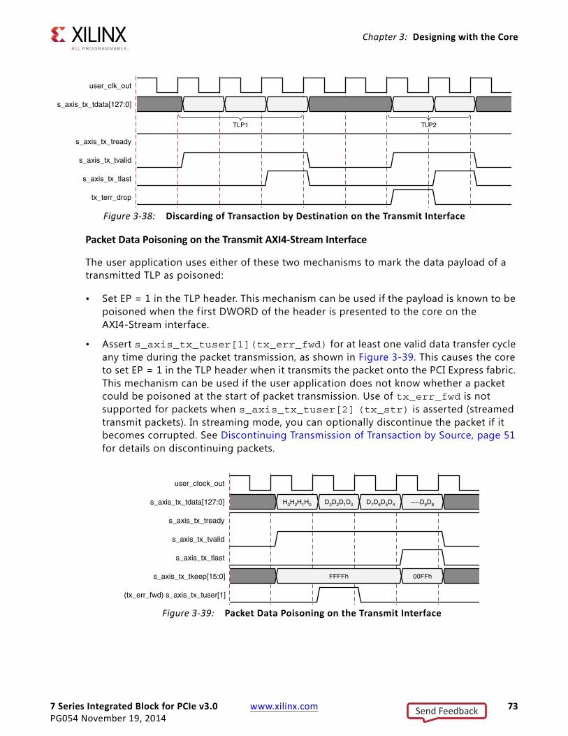
7 Series Integrated Block for PCIe v3.0 www.xilinx.com 73PG054 November 19, 2014
Chapter 3: Designing with the Core
Packet Data Poisoning on the Transmit AXI4-Stream Interface
The user application uses either of these two mechanisms to mark the data payload of a transmitted TLP as poisoned:
• Set EP = 1 in the TLP header. This mechanism can be used if the payload is known to be poisoned when the f irst DWORD of the header is presented to the core on the AXI4-Stream interface.
• Assert s_axis_tx_tuser[1](tx_err_fwd) for at least one valid data transfer cycle any time during the packet transmission, as shown in Figure 3-39. This causes the core to set EP = 1 in the TLP header when it transmits the packet onto the PCI Express fabric. This mechanism can be used if the user application does not know whether a packet could be poisoned at the start of packet transmission. Use of tx_err_fwd is not supported for packets when s_axis_tx_tuser[2] (tx_str) is asserted (streamed transmit packets). In streaming mode, you can optionally discontinue the packet if it becomes corrupted. See Discontinuing Transmission of Transaction by Source, page 51 for details on discontinuing packets.
X-Ref Target - Figure 3-38
Figure 3-38: Discarding of Transaction by Destination on the Transmit Interface
user_clk_out
s_axis_tx_tdata[127:0]
s_axis_tx_tready
s_axis_tx_tvalid
s_axis_tx_tlast
tx_terr_drop
TLP1 TLP2
X-Ref Target - Figure 3-39
Figure 3-39: Packet Data Poisoning on the Transmit Interface
user_clock_out
s_axis_tx_tdata[127:0]
s_axis_tx_tready
s_axis_tx_tvalid
s_axis_tx_tlast
s_axis_tx_tkeep[15:0]
(tx_err_fwd) s_axis_tx_tuser[1]
H3H2H1H0 D3D2D1D0 D7D6D5D4 ----D9D8
FFFFh 00FFh
Send Feedback
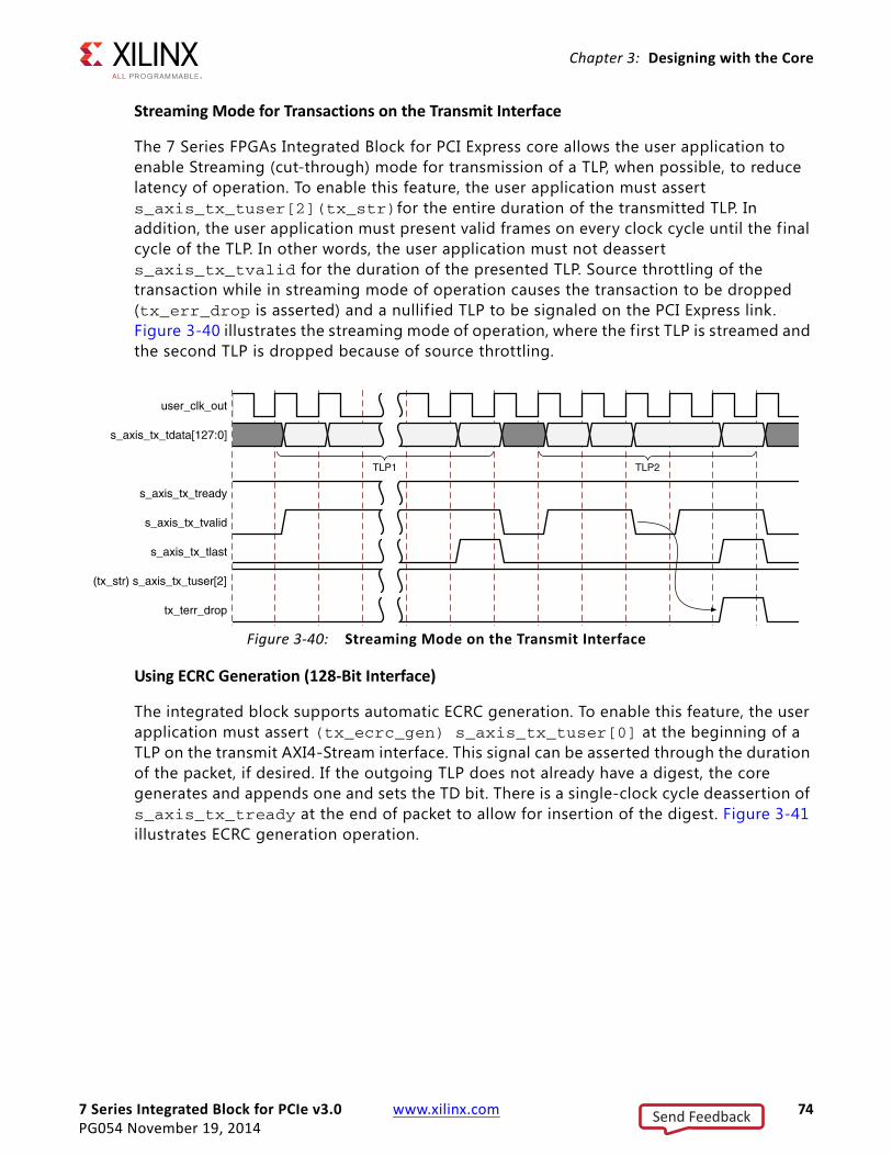
7 Series Integrated Block for PCIe v3.0 www.xilinx.com 74PG054 November 19, 2014
Chapter 3: Designing with the Core
Streaming Mode for Transactions on the Transmit Interface
The 7 Series FPGAs Integrated Block for PCI Express core allows the user application to enable Streaming (cut-through) mode for transmission of a TLP, when possible, to reduce latency of operation. To enable this feature, the user application must assert s_axis_tx_tuser[2](tx_str)for the entire duration of the transmitted TLP. In addition, the user application must present valid frames on every clock cycle until the final cycle of the TLP. In other words, the user application must not deassert s_axis_tx_tvalid for the duration of the presented TLP. Source throttling of the transaction while in streaming mode of operation causes the transaction to be dropped (tx_err_drop is asserted) and a nullif ied TLP to be signaled on the PCI Express link. Figure 3-40 illustrates the streaming mode of operation, where the first TLP is streamed and the second TLP is dropped because of source throttling.
Using ECRC Generation (128-Bit Interface)
The integrated block supports automatic ECRC generation. To enable this feature, the user application must assert (tx_ecrc_gen) s_axis_tx_tuser[0] at the beginning of a TLP on the transmit AXI4-Stream interface. This signal can be asserted through the duration of the packet, if desired. If the outgoing TLP does not already have a digest, the core generates and appends one and sets the TD bit. There is a single-clock cycle deassertion of s_axis_tx_tready at the end of packet to allow for insertion of the digest. Figure 3-41 illustrates ECRC generation operation.
X-Ref Target - Figure 3-40
Figure 3-40: Streaming Mode on the Transmit Interface
user_clk_out
s_axis_tx_tdata[127:0]
s_axis_tx_tready
s_axis_tx_tvalid
s_axis_tx_tlast
(tx_str) s_axis_tx_tuser[2]
tx_terr_drop
TLP1 TLP2
Send Feedback
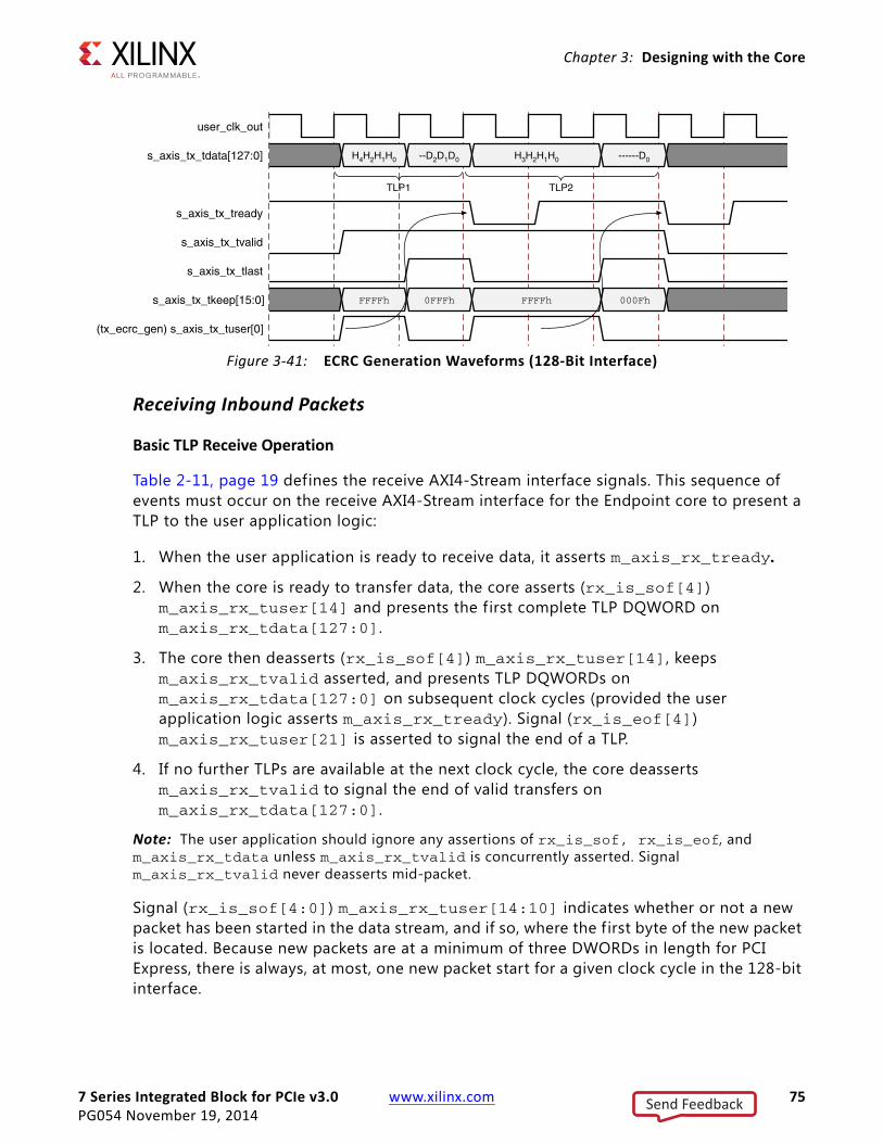
7 Series Integrated Block for PCIe v3.0 www.xilinx.com 75PG054 November 19, 2014
Chapter 3: Designing with the Core
Receiving Inbound Packets
Basic TLP Receive Operation
Table 2-11, page 19 defines the receive AXI4-Stream interface signals. This sequence of events must occur on the receive AXI4-Stream interface for the Endpoint core to present a TLP to the user application logic:
1. When the user application is ready to receive data, it asserts m_axis_rx_tready.
2. When the core is ready to transfer data, the core asserts (rx_is_sof[4]) m_axis_rx_tuser[14] and presents the f irst complete TLP DQWORD on m_axis_rx_tdata[127:0].
3. The core then deasserts (rx_is_sof[4]) m_axis_rx_tuser[14], keeps m_axis_rx_tvalid asserted, and presents TLP DQWORDs on m_axis_rx_tdata[127:0] on subsequent clock cycles (provided the user application logic asserts m_axis_rx_tready). Signal (rx_is_eof[4]) m_axis_rx_tuser[21] is asserted to signal the end of a TLP.
4. If no further TLPs are available at the next clock cycle, the core deasserts m_axis_rx_tvalid to signal the end of valid transfers on m_axis_rx_tdata[127:0].
Note: The user application should ignore any assertions of rx_is_sof, rx_is_eof, and m_axis_rx_tdata unless m_axis_rx_tvalid is concurrently asserted. Signal m_axis_rx_tvalid never deasserts mid-packet.
Signal (rx_is_sof[4:0]) m_axis_rx_tuser[14:10] indicates whether or not a new packet has been started in the data stream, and if so, where the f irst byte of the new packet is located. Because new packets are at a minimum of three DWORDs in length for PCI Express, there is always, at most, one new packet start for a given clock cycle in the 128-bit interface.
X-Ref Target - Figure 3-41
Figure 3-41: ECRC Generation Waveforms (128-Bit Interface)
user_clk_out
s_axis_tx_tdata[127:0]
s_axis_tx_tready
s_axis_tx_tvalid
s_axis_tx_tlast
s_axis_tx_tkeep[15:0]
(tx_ecrc_gen) s_axis_tx_tuser[0]
H4H2H1H0 --D2D1D0 H3H2H1H0 ------D0
FFFFh 0FFFh FFFFh 000Fh
TLP1 TLP2
Send Feedback

7 Series Integrated Block for PCIe v3.0 www.xilinx.com 76PG054 November 19, 2014
Chapter 3: Designing with the Core
The rx_is_sof[2:0] signal is always deasserted for the 128-bit interface; you can decode rx_is_sof[3:2] to determine in which DWORD the EOF occurs.
• rx_is_sof = 5'b10000 - SOF located at byte 0 (DWORD 0)
• rx_is_sof = 5'b11000 - SOF located at byte 8 (DWORD 2)
• rx_is_sof = 5'b0XXXX - SOF not present
The (rx_is_eof[4:0]) m_axis_rx_tuser[21:17] signal indicates whether or not a current packet is ending in the data stream, and if so, where the last byte of the current packet is located. Because packets are at a minimum of three DWORDs in length for PCI Express, there is always, at most, one packet ending for a given clock cycle in the 128-bit interface.
The rx_is_eof[1:0] signal is always asserted for the 128-bit interface; you can decode rx_is_eof[3:2] to determine in which DWORD the EOF occurs. These rx_is_eof values are valid for PCI Express:
• rx_is_eof = 5'b10011 - EOF located at byte 3 (DWORD 0)
• rx_is_eof = 5'b10111 - EOF located at byte 7 (DWORD 1)
• rx_is_eof = 5'b11011 - EOF located at byte 11 (DWORD 2)
• rx_is_eof = 5'b11111 - EOF located at byte 15 (DWORD 3)
• rx_is_eof = 5'b0XXXX - EOF not present
Table 3-6 through Table 3-9 use the notation Hn and Dn to denote Header DWORD n and Data DWORD n, respectively. Table 3-6 list the signaling for all the valid cases where a packet can start and end within a single beat (single-cycle TLP).
Table 3-4: rx_is_sof Signal Description
Bit Description
rx_is_sof[3:0] Binary encoded byte location of start-of-frame (SOF): 4'b0000 = byte 0, 4'b1111 = byte 15
rx_is_sof[4] Assertion indicates a new packet has been started in the current RX data.
Table 3-5: rx_is_eof Signal Description
Bit Description
rx_is_eof[3:0] Binary encoded byte location of EOF: 4'b0000 = byte 0, 4'b1111 = byte 15
rx_is_eof[4] Assertion indicates a packet is ending in the current RX data.
Send Feedback

7 Series Integrated Block for PCIe v3.0 www.xilinx.com 77PG054 November 19, 2014
Chapter 3: Designing with the Core
Table 3-7 lists the signaling for all multicycle, non-straddled TLP SOF scenarios.
Table 3-8 lists the possible signaling for ending a multicycle packet. If a packet ends in the lower QWORD of the data bus, the next packet can start in the upper QWORD of that beat (see Straddle cases, Table 3-9). rx_is_eof[3:2] indicates which DW the EOF occurs.
Table 3-9 lists the possible signaling for a straddled data transfer beat. A straddled data transfer beat occurs when one packet ends in the lower QWORD and a new packet starts in the upper QWORD of the same cycle. Straddled data transfers only occur in the receive direction.
Table 3-6: Single-Cycle SOF and EOF Scenarios (Header and Header with Data)
m_axis_rx_tdata[127:0]
H3 H2 H1 H0 -- H2 H1 H0 D0 H2 H1 H0
rx_is_sof[4] 1b 1b 1b
rx_is_sof[3:0] 0000b 0000b 0000b
rx_is_eof[4] 1b 1b 1b
rx_is_eof[3:0] 1111b 1011b 1111b
Table 3-7: Multicycle, Non-Straddled SOF Scenarios
m_axis_rx_tdata[127:0]
H3 H2 H1 H0(1) D0 H2 H1 H0(2) H1 H0 -- --(3)
rx_is_sof[4] 1b 1b 1b
rx_is_sof[3:0] 0000b 0000b 1000b
rx_is_eof[4] 0b 0b 0b
rx_is_eof[3:0] xxxxb xxxxb xxxxb
Notes: 1. Data begins on the next clock cycle.2. Data continues on the next clock cycle.3. Remainder of header and possible data on the next clock cycle.
Table 3-8: Receive - EOF Scenarios (Data)
m_axis_rx_tdata[127:0]
D3 D2 D1 D0 -- D2 D1 D0 -- -- D1 D0 -- -- -- D0
rx_is_sof[4] 0b 0b 0b 0b
rx_is_sof[3:0] 0000b 0000b 0000b 0000b
rx_is_eof[4] 1b 1b 1b 1b
rx_is_eof[3:0] 1111b 1011b 0111b 0011b
Send Feedback
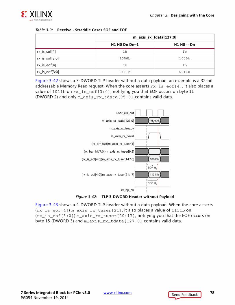
7 Series Integrated Block for PCIe v3.0 www.xilinx.com 78PG054 November 19, 2014
Chapter 3: Designing with the Core
Figure 3-42 shows a 3-DWORD TLP header without a data payload; an example is a 32-bit addressable Memory Read request. When the core asserts rx_is_eof[4], it also places a value of 1011b on rx_is_eof[3:0], notifying you that EOF occurs on byte 11 (DWORD 2) and only m_axis_rx_tdata[95:0] contains valid data.
Figure 3-43 shows a 4-DWORD TLP header without a data payload. When the core asserts (rx_is_eof[4]) m_axis_rx_tuser[21], it also places a value of 1111b on (rx_is_eof[3:0]) m_axis_rx_tuser[20:17], notifying you that the EOF occurs on byte 15 (DWORD 3) and m_axis_rx_tdata[127:0] contains valid data.
Table 3-9: Receive - Straddle Cases SOF and EOF
m_axis_rx_tdata[127:0]
H1 H0 Dn Dn–1 H1 H0 -- Dn
rx_is_sof[4] 1b 1b
rx_is_sof[3:0] 1000b 1000b
rx_is_eof[4] 1b 1b
rx_is_eof[3:0] 0111b 0011b
X-Ref Target - Figure 3-42
Figure 3-42: TLP 3-DWORD Header without Payload
user_clk_out
m_axis_rx_tdata[127:0]
m_axis_rx_tready
m_axis_rx_tvalid
(rx_err_fwd)m_axis_rx_tuser[1]
(rx_bar_hit[7:0])m_axis_rx_tuser[9:2]
(rx_is_sof[4:0])m_axis_rx_tuser[14:10]
(rx_is_eof[4:0])m_axis_rx_tuser[21:17]
rx_np_ok
--H2H1H0
10000b
11011b
SOF H0
EOF H2
Send Feedback
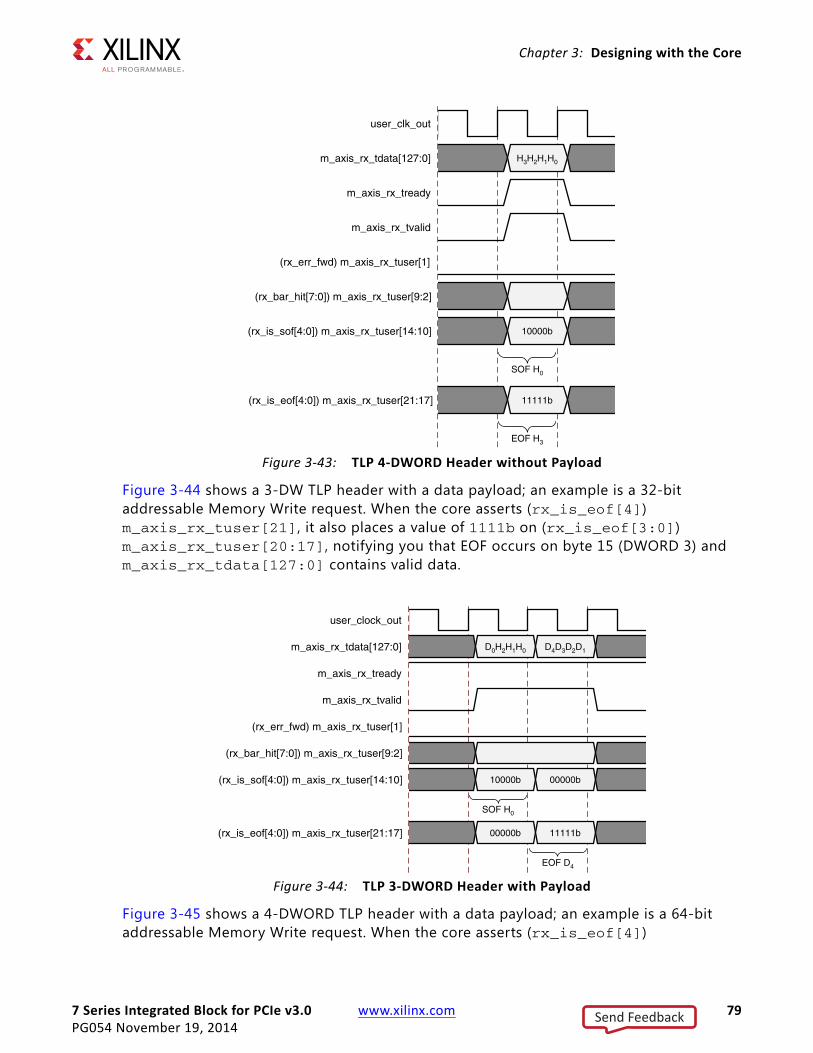
7 Series Integrated Block for PCIe v3.0 www.xilinx.com 79PG054 November 19, 2014
Chapter 3: Designing with the Core
Figure 3-44 shows a 3-DW TLP header with a data payload; an example is a 32-bit addressable Memory Write request. When the core asserts (rx_is_eof[4]) m_axis_rx_tuser[21], it also places a value of 1111b on (rx_is_eof[3:0]) m_axis_rx_tuser[20:17], notifying you that EOF occurs on byte 15 (DWORD 3) and m_axis_rx_tdata[127:0] contains valid data.
Figure 3-45 shows a 4-DWORD TLP header with a data payload; an example is a 64-bit addressable Memory Write request. When the core asserts (rx_is_eof[4])
X-Ref Target - Figure 3-43
Figure 3-43: TLP 4-DWORD Header without Payload
X-Ref Target - Figure 3-44
Figure 3-44: TLP 3-DWORD Header with Payload
user_clk_out
m_axis_rx_tdata[127:0]
m_axis_rx_tready
m_axis_rx_tvalid
(rx_err_fwd) m_axis_rx_tuser[1]
(rx_bar_hit[7:0]) m_axis_rx_tuser[9:2]
(rx_is_sof[4:0]) m_axis_rx_tuser[14:10]
(rx_is_eof[4:0]) m_axis_rx_tuser[21:17]
H3H2H1H0
10000b
11111b
SOF H0
EOF H3
user_clock_out
m_axis_rx_tdata[127:0]
m_axis_rx_tready
m_axis_rx_tvalid
(rx_err_fwd) m_axis_rx_tuser[1]
(rx_bar_hit[7:0]) m_axis_rx_tuser[9:2]
(rx_is_sof[4:0]) m_axis_rx_tuser[14:10]
(rx_is_eof[4:0]) m_axis_rx_tuser[21:17]
D0H2H1H0 D4D3D2D1
10000b 00000b
00000b 11111b
SOF H0
EOF D4
Send Feedback
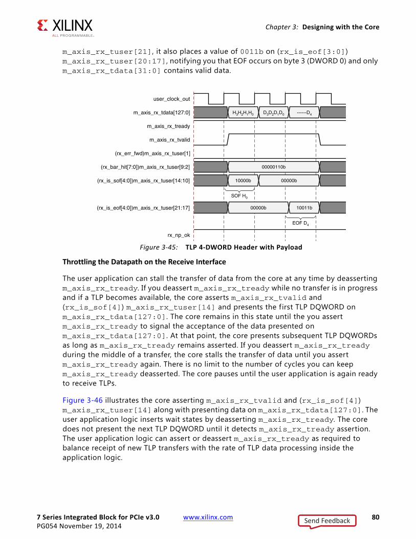
7 Series Integrated Block for PCIe v3.0 www.xilinx.com 80PG054 November 19, 2014
Chapter 3: Designing with the Core
m_axis_rx_tuser[21], it also places a value of 0011b on (rx_is_eof[3:0]) m_axis_rx_tuser[20:17], notifying you that EOF occurs on byte 3 (DWORD 0) and only m_axis_rx_tdata[31:0] contains valid data.
Throttling the Datapath on the Receive Interface
The user application can stall the transfer of data from the core at any time by deasserting m_axis_rx_tready. If you deassert m_axis_rx_tready while no transfer is in progress and if a TLP becomes available, the core asserts m_axis_rx_tvalid and (rx_is_sof[4]) m_axis_rx_tuser[14] and presents the f irst TLP DQWORD on m_axis_rx_tdata[127:0]. The core remains in this state until the you assert m_axis_rx_tready to signal the acceptance of the data presented on m_axis_rx_tdata[127:0]. At that point, the core presents subsequent TLP DQWORDs as long as m_axis_rx_tready remains asserted. If you deassert m_axis_rx_tready during the middle of a transfer, the core stalls the transfer of data until you assert m_axis_rx_tready again. There is no limit to the number of cycles you can keep m_axis_rx_tready deasserted. The core pauses until the user application is again ready to receive TLPs.
Figure 3-46 illustrates the core asserting m_axis_rx_tvalid and (rx_is_sof[4]) m_axis_rx_tuser[14] along with presenting data on m_axis_rx_tdata[127:0]. The user application logic inserts wait states by deasserting m_axis_rx_tready. The core does not present the next TLP DQWORD until it detects m_axis_rx_tready assertion. The user application logic can assert or deassert m_axis_rx_tready as required to balance receipt of new TLP transfers with the rate of TLP data processing inside the application logic.
X-Ref Target - Figure 3-45
Figure 3-45: TLP 4-DWORD Header with Payload
user_clock_out
m_axis_rx_tdata[127:0]
m_axis_rx_tready
m_axis_rx_tvalid
(rx_err_fwd)m_axis_rx_tuser[1]
(rx_bar_hit[7:0])m_axis_rx_tuser[9:2]
(rx_is_sof[4:0])m_axis_rx_tuser[14:10]
(rx_is_eof[4:0])m_axis_rx_tuser[21:17]
rx_np_ok
H3H2H1H0 D3D2D1D0 ------D4
00000110b
10000b 00000b
00000b 10011b
SOF H0
EOF D4
Send Feedback
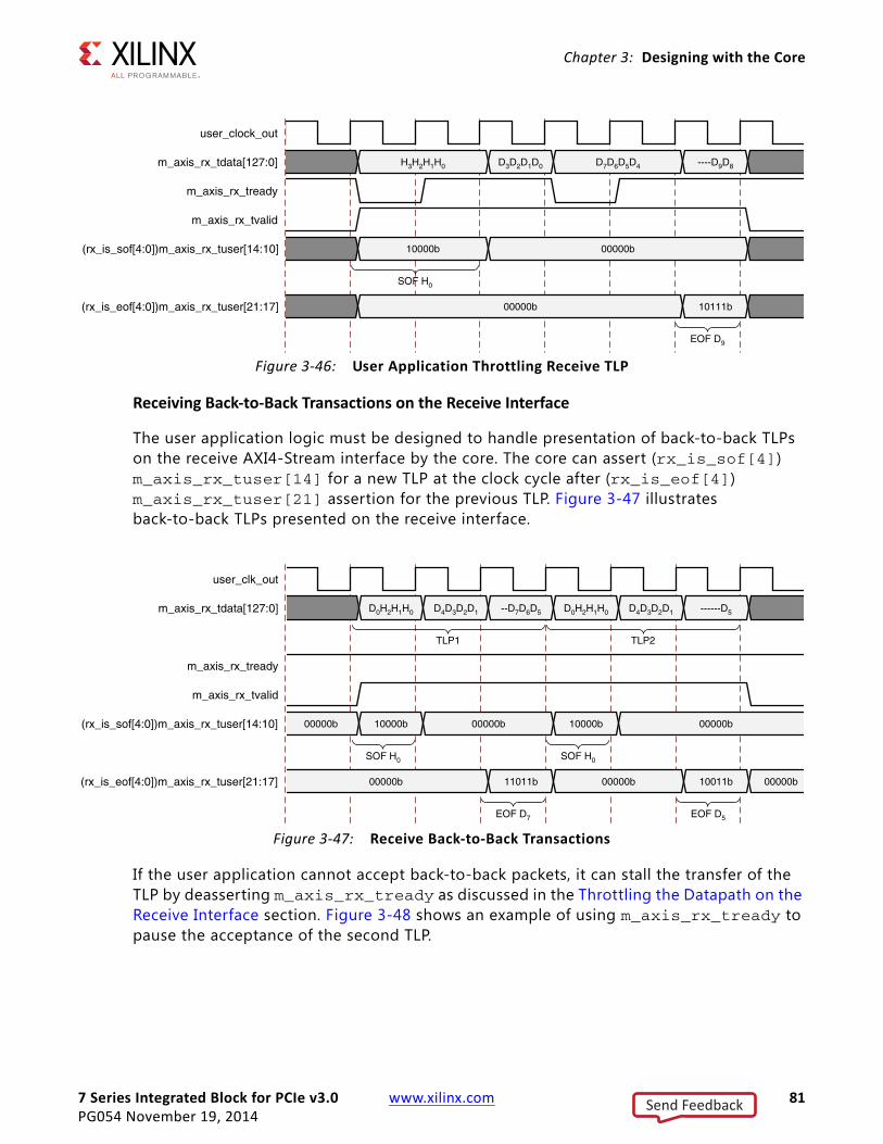
7 Series Integrated Block for PCIe v3.0 www.xilinx.com 81PG054 November 19, 2014
Chapter 3: Designing with the Core
Receiving Back-to-Back Transactions on the Receive Interface
The user application logic must be designed to handle presentation of back-to-back TLPs on the receive AXI4-Stream interface by the core. The core can assert (rx_is_sof[4]) m_axis_rx_tuser[14] for a new TLP at the clock cycle after (rx_is_eof[4]) m_axis_rx_tuser[21] assertion for the previous TLP. Figure 3-47 illustrates back-to-back TLPs presented on the receive interface.
If the user application cannot accept back-to-back packets, it can stall the transfer of the TLP by deasserting m_axis_rx_tready as discussed in the Throttling the Datapath on the Receive Interface section. Figure 3-48 shows an example of using m_axis_rx_tready to pause the acceptance of the second TLP.
X-Ref Target - Figure 3-46
Figure 3-46: User Application Throttling Receive TLP
user_clock_out
m_axis_rx_tdata[127:0]
m_axis_rx_tready
m_axis_rx_tvalid
(rx_is_sof[4:0])m_axis_rx_tuser[14:10]
(rx_is_eof[4:0])m_axis_rx_tuser[21:17]
H3H2H1H0 D3D2D1D0 D7D6D5D4 ----D9D8
10000b 00000b
00000b 10111b
SOF H0
EOF D9
X-Ref Target - Figure 3-47
Figure 3-47: Receive Back-to-Back Transactions
user_clk_out
m_axis_rx_tdata[127:0]
m_axis_rx_tready
m_axis_rx_tvalid
(rx_is_sof[4:0])m_axis_rx_tuser[14:10]
(rx_is_eof[4:0])m_axis_rx_tuser[21:17]
D0H2H1H0 D4D3D2D1 --D7D6D5 D0H2H1H0 D4D3D2D1 ------D5
00000b 10000b 00000b 10000b 00000b
00000b 11011b 00000b 10011b 00000b
TLP1 TLP2
SOF H0 SOF H0
EOF D7 EOF D5
Send Feedback
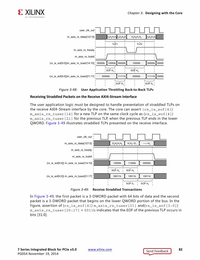
7 Series Integrated Block for PCIe v3.0 www.xilinx.com 82PG054 November 19, 2014
Chapter 3: Designing with the Core
Receiving Straddled Packets on the Receive AXI4-Stream Interface
The user application logic must be designed to handle presentation of straddled TLPs on the receive AXI4-Stream interface by the core. The core can assert (rx_is_sof[4]) m_axis_rx_tuser[14] for a new TLP on the same clock cycle as (rx_is_eof[4]) m_axis_rx_tuser[21] for the previous TLP, when the previous TLP ends in the lower QWORD. Figure 3-49 illustrates straddled TLPs presented on the receive interface.
In Figure 3-49, the first packet is a 3-DWORD packet with 64 bits of data and the second packet is a 3-DWORD packet that begins on the lower QWORD portion of the bus. In the f igure, assertion of (rx_is_eof[4]) m_axis_rx_tuser[21] and(rx_is_eof[3:0]) m_axis_rx_tuser[20:17] = 0011b indicates that the EOF of the previous TLP occurs in bits [31:0].
X-Ref Target - Figure 3-48
Figure 3-48: User Application Throttling Back-to-Back TLPs
X-Ref Target - Figure 3-49
Figure 3-49: Receive Straddled Transactions
user_clk_out
m_axis_rx_tdata[127:0]
m_axis_rx_tready
m_axis_rx_tvalid
(rx_is_sof[4:0])m_axis_rx_tuser[14:10]
(rx_is_eof[4:0])m_axis_rx_tuser[21:17]
D0H2H1H0D4D3D2D1 H3H2H1H0 D3D2D1D0
00000b 10000b 00000b 10000b 00000b 00000b
00000b 11111b 00000b 11111b 00000b
TLP1 TLP2
SOF H0 SOF H0
EOF D4 EOF D3
user_clk_out
m_axis_rx_tdata[127:0]
m_axis_rx_tready
m_axis_rx_tvalid
(rx_is_sof[4:0]) m_axis_rx_tuser[14:10]
(rx_is_eof[4:0]) m_axis_rx_tuser[21:17]
D0H2H1H0 H1H0--D1 ------H2
10000b 11000b 00000b
00011b 10011b 10011b
SOF H0 SOF H0
EOF D1 EOF H2
Send Feedback
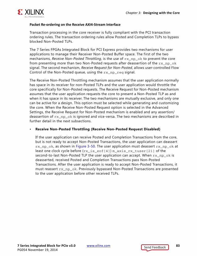
7 Series Integrated Block for PCIe v3.0 www.xilinx.com 83PG054 November 19, 2014
Chapter 3: Designing with the Core
Packet Re-ordering on the Receive AXI4-Stream Interface
Transaction processing in the core receiver is fully compliant with the PCI transaction ordering rules. The transaction ordering rules allow Posted and Completion TLPs to bypass blocked Non-Posted TLPs.
The 7 Series FPGAs Integrated Block for PCI Express provides two mechanisms for user applications to manage their Receiver Non-Posted Buffer space. The f irst of the two mechanisms, Receive Non-Posted Throttling, is the use of rx_np_ok to prevent the core from presenting more than two Non-Posted requests after deassertion of the rx_np_ok signal. The second mechanism, Receive Request for Non-Posted, allows user-controlled Flow Control of the Non-Posted queue, using the rx_np_req signal.
The Receive Non-Posted Throttling mechanism assumes that the user application normally has space in its receiver for non-Posted TLPs and the user application would throttle the core specif ically for Non-Posted requests. The Receive Request for Non-Posted mechanism assumes that the user application requests the core to present a Non-Posted TLP as and when it has space in its receiver. The two mechanisms are mutually exclusive, and only one can be active for a design. This option must be selected while generating and customizing the core. When the Receive Non-Posted Request option is selected in the Advanced Settings, the Receive Request for Non-Posted mechanism is enabled and any assertion/deassertion of rx_np_ok is ignored and vice-versa. The two mechanisms are described in further detail in the next subsections.
• Receive Non-Posted Throttling (Receive Non-Posted Request Disabled)
If the user application can receive Posted and Completion Transactions from the core, but is not ready to accept Non-Posted Transactions, the user application can deassert rx_np_ok , as shown in Figure 3-50. The user application must deassert rx_np_ok at least one clock cycle before (rx_is_eof[4]) m_axis_rx_tuser[21] of the second-to-last Non-Posted TLP the user application can accept. When rx_np_ok is deasserted, received Posted and Completion Transactions pass Non-Posted Transactions. After the user application is ready to accept Non-Posted Transactions, it must reassert rx_np_ok . Previously bypassed Non-Posted Transactions are presented to the user application before other received TLPs.
Send Feedback
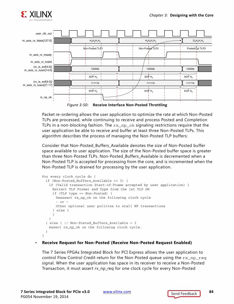
7 Series Integrated Block for PCIe v3.0 www.xilinx.com 84PG054 November 19, 2014
Chapter 3: Designing with the Core
Packet re-ordering allows the user application to optimize the rate at which Non-Posted TLPs are processed, while continuing to receive and process Posted and Completion TLPs in a non-blocking fashion. The rx_np_ok signaling restrictions require that the user application be able to receive and buffer at least three Non-Posted TLPs. This algorithm describes the process of managing the Non-Posted TLP buffers:
Consider that Non-Posted_Buffers_Available denotes the size of Non-Posted buffer space available to user application. The size of the Non-Posted buffer space is greater than three Non-Posted TLPs. Non-Posted_Buffers_Available is decremented when a Non-Posted TLP is accepted for processing from the core, and is incremented when the Non-Posted TLP is drained for processing by the user application.
For every clock cycle do {if (Non-Posted_Buffers_Available <= 3) {if (Valid transaction Start-of-Frame accepted by user application) {Extract TLP Format and Type from the 1st TLP DWif (TLP type == Non-Posted) {Deassert rx_np_ok on the following clock cycle- or -Other optional user policies to stall NP transactions
} else {}
}} else { // Non-Posted_Buffers_Available > 3Assert rx_np_ok on the following clock cycle.
}}
• Receive Request for Non-Posted (Receive Non-Posted Request Enabled)
The 7 Series FPGAs Integrated Block for PCI Express allows the user application to control Flow Control Credit return for the Non-Posted queue using the rx_np_req signal. When the user application has space in its receiver to receive a Non-Posted Transaction, it must assert rx_np_req for one clock cycle for every Non-Posted
X-Ref Target - Figure 3-50
Figure 3-50: Receive Interface Non-Posted Throttling
user_clk_out
m_axis_rx_tdata[127:0]
m_axis_rx_tready
m_axis_rx_tvalid
(rx_is_sof[4:0])m_axis_rx_tuser[14:0]
(rx_is_eof[4:0])m_axis_rx_tuser[21:17]
rx_np_ok
H3H2H1H0 H3H2H1H0 D0H2H1H0
10000b 10000b 10000b
11111b 11111b 11111b
Non-Posted TLP1 Non-Posted TLP2 Posted/Cpl TLP3
SOF H0 SOF H0 SOF H0
EOF H3 EOF H3 EOF D0
Send Feedback

7 Series Integrated Block for PCIe v3.0 www.xilinx.com 85PG054 November 19, 2014
Chapter 3: Designing with the Core
Transaction that the user application can accept. This enables the integrated block to present one Non-Posted transaction from its receiver queues to the core transaction interface, as shown in Figure 3-51 and return one Non-Posted Credit to the connected Link partner.
The 7 Series Integrated Block for PCIe maintains a count of up to 12 Non-Posted Requests from the user application. In other words, the core remembers assertions of rx_np_req even if no Non-Posted TLPs are present in the receive buffer and presents received Non-Posted TLPs to the user application, if requests have been previously made by the user application. If the core has no outstanding requests from the user application and received Non-Posted TLPs are waiting in the receive buffer, received Posted and Completion Transactions pass the waiting Non-Posted Transactions. After the user application is ready to accept a Non-Posted TLP, asserting rx_np_req for one or more cycles causes that number of waiting Non-Posted TLPs to be delivered at the next available TLP boundary. In other words, any Posted or Completion TLP currently on the user application interface finishes before waiting Non-Posted TLPs are presented to the user application. If there are no Posted or Completion TLPs being presented and a Non-Posted TLP is waiting, assertion of rx_np_req causes the Non-Posted TLP to be presented to the user application. TLPs are delivered to the user application in order except when you are throttling Non-Posted TLPs, allowing Posted and Completion TLPs to pass. When you start accepting Non-Posted TLPs again, ordering is still maintained with any subsequent Posted or Completion TLPs. If the user application can accept all Non-Posted Transactions as they are received and does not care about controlling the Flow Control Credit return for the Non-Posted queue, keep this signal asserted.
X-Ref Target - Figure 3-51
Figure 3-51: Receive Interface Request for Non-Posted Transaction
user_clk_out
m_axis_rx_tdata[127:0]
m_axis_rx_tready
m_axis_rx_tvalid
(rx_is_sof[4:0]) m_axis_rx_tuser[14:10]
(rx_is_eof[4:0]) m_axis_rx_tuser[21:17]
rx_np_req
D0H2H1H0D4D3D2D1--H2H1H0D0H2H1H0 ----D2D1 H3H2H1H0--H2H1H0
10000b 00000b 10000b 10000b 00000b 00000b 10000b 10000b
00011b 11111b 11011b 00011b 10111b 00011b 11111b 11011b
Posted TLP1 Posted/Cpl TLP3 Non-Posted TLP5
Non-Posted TLP2 Non-Posted TLP4
SOF H0 SOF H0 SOF H0 SOF H0 SOF H0
EOF D4 EOF H2 EOF D2 EOF H3 EOF H2
Send Feedback
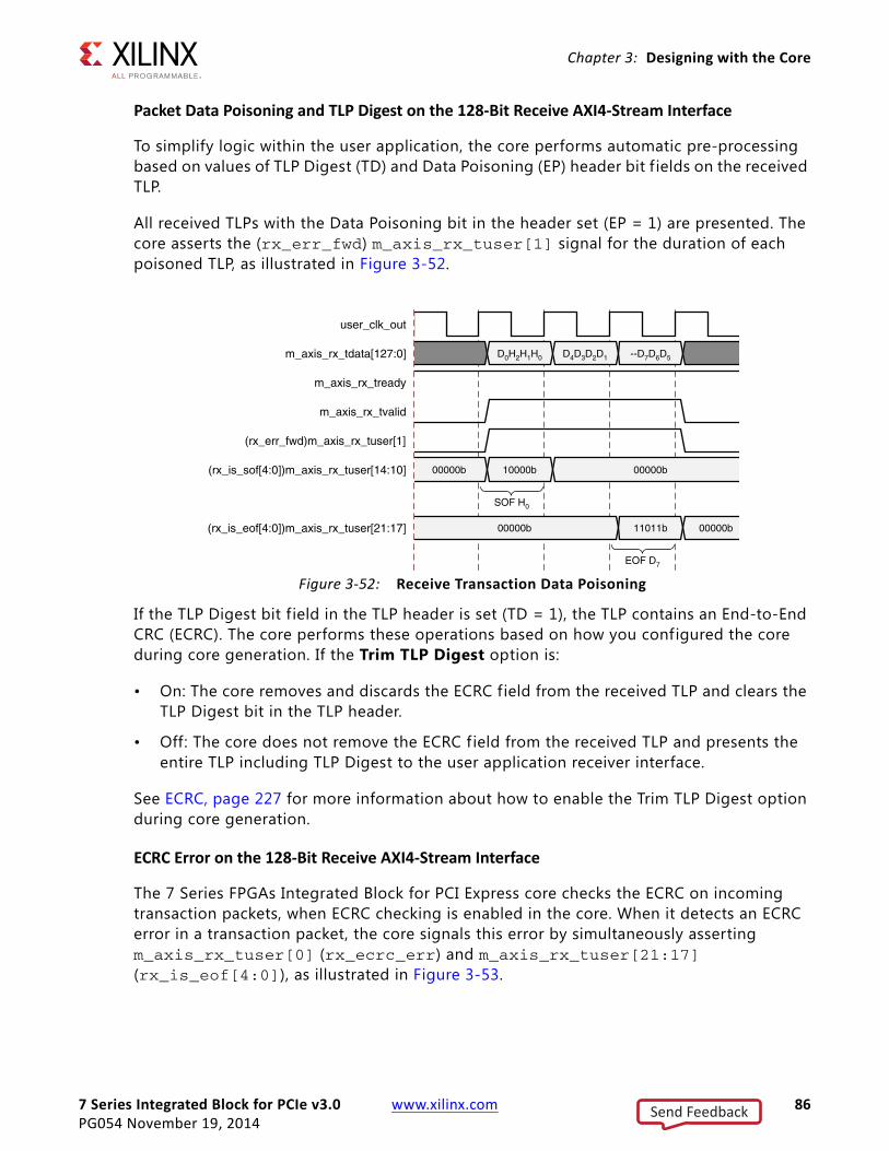
7 Series Integrated Block for PCIe v3.0 www.xilinx.com 86PG054 November 19, 2014
Chapter 3: Designing with the Core
Packet Data Poisoning and TLP Digest on the 128-Bit Receive AXI4-Stream Interface
To simplify logic within the user application, the core performs automatic pre-processing based on values of TLP Digest (TD) and Data Poisoning (EP) header bit f ields on the received TLP.
All received TLPs with the Data Poisoning bit in the header set (EP = 1) are presented. The core asserts the (rx_err_fwd) m_axis_rx_tuser[1] signal for the duration of each poisoned TLP, as illustrated in Figure 3-52.
If the TLP Digest bit f ield in the TLP header is set (TD = 1), the TLP contains an End-to-End CRC (ECRC). The core performs these operations based on how you configured the core during core generation. If the Trim TLP Digest option is:
• On: The core removes and discards the ECRC field from the received TLP and clears the TLP Digest bit in the TLP header.
• Off: The core does not remove the ECRC field from the received TLP and presents the entire TLP including TLP Digest to the user application receiver interface.
See ECRC, page 227 for more information about how to enable the Trim TLP Digest option during core generation.
ECRC Error on the 128-Bit Receive AXI4-Stream Interface
The 7 Series FPGAs Integrated Block for PCI Express core checks the ECRC on incoming transaction packets, when ECRC checking is enabled in the core. When it detects an ECRC error in a transaction packet, the core signals this error by simultaneously asserting m_axis_rx_tuser[0] (rx_ecrc_err) and m_axis_rx_tuser[21:17] (rx_is_eof[4:0]), as illustrated in Figure 3-53.
X-Ref Target - Figure 3-52
Figure 3-52: Receive Transaction Data Poisoning
user_clk_out
m_axis_rx_tdata[127:0]
m_axis_rx_tready
m_axis_rx_tvalid
(rx_err_fwd)m_axis_rx_tuser[1]
(rx_is_sof[4:0])m_axis_rx_tuser[14:10]
(rx_is_eof[4:0])m_axis_rx_tuser[21:17]
D0H2H1H0 D4D3D2D1 --D7D6D5
00000b 10000b 00000b
00000b 11011b 00000b
SOF H0
EOF D7
Send Feedback

7 Series Integrated Block for PCIe v3.0 www.xilinx.com 87PG054 November 19, 2014
Chapter 3: Designing with the Core
Packet Base Address Register Hit on the Receive AXI4-Stream Interface
The core decodes incoming Memory and I/O TLP request addresses to determine which Base Address Register (BAR) in the core Type0 configuration space is being targeted, and indicates the decoded base address on (rx_bar_hit[7:0]) m_axis_rx_tuser[9:2]. For each received Memory or I/O TLP, a minimum of one and a maximum of two (adjacent) bits are set to 1. If the received TLP targets a 32-bit Memory or I/O BAR, only one bit is asserted. If the received TLP targets a 64-bit Memory BAR, two adjacent bits are asserted. If the core receives a TLP that is not decoded by one of the BARs, then the core drops it without presenting it, and it automatically generates an Unsupported Request message. Even if the core is configured for a 64-bit BAR, the system might not always allocate a 64-bit address, in which case only one rx_bar_hit[7:0] signal is asserted.
Table 3-10 illustrates mapping between rx_bar_hit[7:0] and the BARs, and the corresponding byte offsets in the core Type0 configuration header.
For a Memory or I/O TLP Transaction on the receive interface, rx_bar_hit[7:0] is valid for the entire TLP, starting with the assertion of (rx_is_sof[4])
X-Ref Target - Figure 3-53
Figure 3-53: ECRC Error on 128-Bit Receive AXI4-Stream Interface
Table 3-10: rx_bar_hit to Base Address Register Mapping
rx_bar_hit[x] m_axis_rx_tuser[x] BAR Byte Offset
0 2 0 10h
1 3 1 14h
2 4 2 18h
3 5 3 1Ch
4 6 4 20h
5 7 5 24h
6 8 Expansion ROM BAR 30h
7 9 Reserved –
user_clk_out
m_axis_rx_tdata[127:0]
m_axis_rx_tready
m_axis_rx_tvalid
(rx_ecrc_err)m_axis_rx_tuser[0]
(rx_is_sof)m_axis_rx_tuser[14:10]
(rx_is_eof)m_axis_rx_tuser[21:17]
D0H2H1H0 D4D3D2D1 --D7D6D5
00000b 10000b 00000b
00000b 11011b 00000b
SOF H0
EOF D7
Send Feedback

7 Series Integrated Block for PCIe v3.0 www.xilinx.com 88PG054 November 19, 2014
Chapter 3: Designing with the Core
m_axis_rx_tuser[14], as shown in Figure 3-54. For straddled data transfer beats, rx_bar_hit[7:0] corresponds to the new packet (the packet corresponding to rx_is_sof[4). When receiving non-Memory and non-I/O transactions, rx_bar_hit[7:0] is undefined.
The (rx_bar_hit[7:0]) m_axis_rx_tuser[9:2] signal enables received Memory and I/O transactions to be directed to the appropriate destination apertures within the user application. By utilizing rx_bar_hit[7:0], application logic can inspect only the lower order Memory and I/O address bits within the address aperture to simplify decoding logic.
Packet Transfer Discontinue on the Receive AXI4-Stream Interface
The loss of communication with the link partner is signaled by deassertion of user_lnk_up. When user_lnk_up is deasserted, it effectively acts as a Hot Reset to the entire core and all TLPs stored inside the core or being presented to the receive interface are irrecoverably lost. A TLP in progress on the Receive AXI4-Stream interface is presented to its correct length, according to the Length f ield in the TLP header. However, the TLP is corrupt and should be discarded by the user application. Figure 3-55 illustrates packet transfer discontinue scenario.
X-Ref Target - Figure 3-54
Figure 3-54: BAR Target Determination Using rx_bar_hit
user_clk_out
m_axis_rx_tdata[127:0]
m_axis_rx_tready
m_axis_rx_tvalid
(rx_is_sof[4:0])m_axis_rx_tuser[14:10]
(rx_is_eof[4:0])m_axis_rx_tuser[21:17]
(rx_bar_hit[7:0])m_axis_rx_tuser[9:2]
H3H2H1H0 D3D2D1D0 D7D6D5D4 D0H2H1H0 D4D3D2D1 D8D7D6D5
10000b 00000b 10000b 00000b
00011b 11111b 00011b 11111b
0000010b 0001100b
TLP1 TLP2
SOF H0 SOF H0
EOF D7 EOF D8
Send Feedback
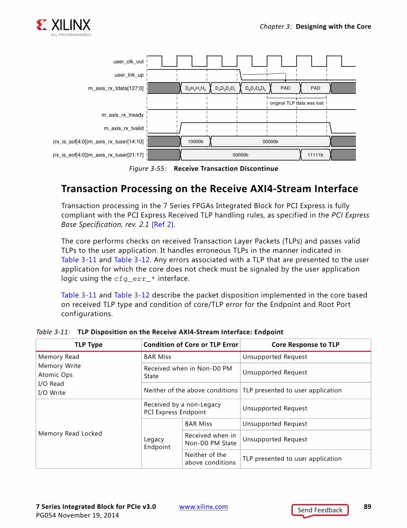
7 Series Integrated Block for PCIe v3.0 www.xilinx.com 89PG054 November 19, 2014
Chapter 3: Designing with the Core
Transaction Processing on the Receive AXI4-Stream InterfaceTransaction processing in the 7 Series FPGAs Integrated Block for PCI Express is fully compliant with the PCI Express Received TLP handling rules, as specif ied in the PCI Express Base Specification, rev. 2.1 [Ref 2].
The core performs checks on received Transaction Layer Packets (TLPs) and passes valid TLPs to the user application. It handles erroneous TLPs in the manner indicated in Table 3-11 and Table 3-12. Any errors associated with a TLP that are presented to the user application for which the core does not check must be signaled by the user application logic using the cfg_err_* interface.
Table 3-11 and Table 3-12 describe the packet disposition implemented in the core based on received TLP type and condition of core/TLP error for the Endpoint and Root Port configurations.
X-Ref Target - Figure 3-55
Figure 3-55: Receive Transaction Discontinue
user_clk_out
user_lnk_up
m_axis_rx_tdata[127:0]
m_axis_rx_tready
m_axis_rx_tvalid
(rx_is_sof[4:0])m_axis_rx_tuser[14:10]
(rx_is_eof[4:0])m_axis_rx_tuser[21:17]
D0H2H1H0 D4D3D2D1 D8D7D6D5 PAD PAD
10000b 00000b
00000b 11111b
original TLP data was lost
Table 3-11: TLP Disposition on the Receive AXI4-Stream Interface: Endpoint
TLP Type Condition of Core or TLP Error Core Response to TLP
Memory ReadMemory WriteAtomic OpsI/O ReadI/O Write
BAR Miss Unsupported Request
Received when in Non-D0 PM State Unsupported Request
Neither of the above conditions TLP presented to user application
Memory Read Locked
Received by a non-Legacy PCI Express Endpoint Unsupported Request
Legacy Endpoint
BAR Miss Unsupported Request
Received when in Non-D0 PM State Unsupported Request
Neither of the above conditions TLP presented to user application
Send Feedback

7 Series Integrated Block for PCIe v3.0 www.xilinx.com 90PG054 November 19, 2014
Chapter 3: Designing with the Core
Configuration Read/Write Type 0Internal Config Space
TLP consumed by the core, to read/write internal Configuration Space and a CplD/Cpl is generated
User-Defined Config Space TLP presented to user application
Configuration Read/Write Type 1 Received by an Endpoint Unsupported Request
CompletionCompletion Locked
Requester ID Miss Unexpected Completion
Received when in Non-D0 PM State Unexpected Completion
Neither of the above conditions TLP presented to user application
Messages
Set Slot Power Limit Received by an Endpoint
TLP consumed by the core and used to program the Captured Slot Power Limit Scale/Value f ields of the Device Capabilities Register
PM_PMEPME_TO_Ack
Received by an Endpoint Unsupported Request
PM_Active_State_NAKPME_Turn_Off
Received by an Endpoint TLP consumed by the core and used to control Power Management
UnlockReceived by a non-Legacy Endpoint Ignored
Received by a Legacy Endpoint TLP presented to user application(1)
INTX Received by an Endpoint Fatal Error
Error_FatalError Non-FatalError Correctable
Received by an Endpoint Unsupported Request
Vendor Defined Type 0Vendor Defined Type 1
Received by an Endpoint TLP presented to user application(1)
Hot Plug Messages Received by an Endpoint TLP dropped by the core
Notes: 1. The TLP is indicated on the cfg_msg* interface and also appears on the m_axis_rx_* interface.
Table 3-11: TLP Disposition on the Receive AXI4-Stream Interface: Endpoint (Cont’d)
TLP Type Condition of Core or TLP Error Core Response to TLP
Table 3-12: TLP Disposition on the Receive AXI4-Stream Interface: Root Port
TLP Type Condition of Core or TLP Error Core Response to TLP
Memory ReadMemory WriteAtomic OpsI/O ReadI/O Write
BAR Miss No BAR Filtering in Root Port configuration: TLP presented to user application
Received when in Non-D0 PM State Unsupported Request
Neither of the above conditions TLP presented to user application
Memory Read Locked Received by a Root Port TLP presented to user application
Send Feedback
7 Series Integrated Block for PCIe v3.0 www.xilinx.com 91PG054 November 19, 2014
Chapter 3: Designing with the Core
Atomic OperationsThe 7 Series FPGAs Integrated Block for PCI Express supports both sending and receiving Atomic operations (Atomic Ops) as defined in the PCI Express Base Specification v2.1. The specification defines three TLP types that allow advanced synchronization mechanisms amongst multiple producers and/or consumers. The integrated block treats Atomic Ops TLPs as Non-Posted Memory Transactions. The three TLP types are:
• FetchAdd
• Swap
• CAS (Compare And Set)
Applications that request Atomic Ops must create the TLP in the user application and send through the transmit AXI4-Stream interface. Applications that respond (complete) to Atomic Ops must receive the TLP from the receive AXI4-Stream interface, create the appropriate completion TLP in the user application, and send the resulting completion through the transmit AXI4-Stream interface.
Configuration Read / Write Type 0 Received by a Root Port Unsupported Request
Configuration Read / Write Type 1 Received by a Root Port Unsupported Request
CompletionCompletion Locked
Received by a Root Port TLP presented to user application
Messages
Set Slot Power Limit Received by a Root Port Unsupported Request
PM_PMEPME_TO_Ack
Received by a Root Port TLP presented to user application(1)
PM_Active_State_NAK Received by a Root Port Unsupported Request
PME_Turn_Off Received by a Root Port Fatal Error
Unlock Received by a Root Port Fatal Error
INTX Received by a Root Port TLP presented to user application(1)
Error_FatalError Non-FatalError Correctable
Received by a Root Port TLP presented to user application(1)
Vendor Defined Type 0Vendor Defined Type 1
Received by a Root Port TLP presented to user application(1)
Hot Plug Messages Received by a Root Port TLP dropped by the core
Notes: 1. The TLP is indicated on the cfg_msg* interface and also appears on the m_axis_rx* interface only if enabled in the Vivado
Integrated Design Environment (IDE).
Table 3-12: TLP Disposition on the Receive AXI4-Stream Interface: Root Port (Cont’d)
TLP Type Condition of Core or TLP Error Core Response to TLP
Send Feedback
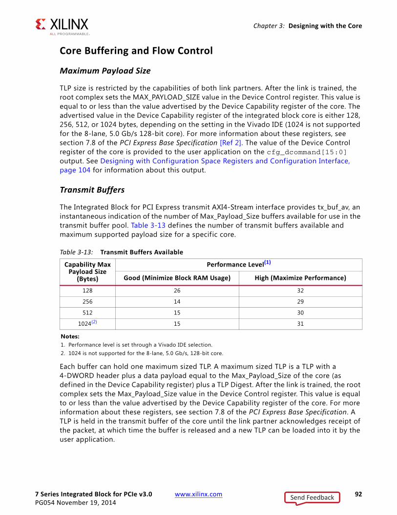
7 Series Integrated Block for PCIe v3.0 www.xilinx.com 92PG054 November 19, 2014
Chapter 3: Designing with the Core
Core Buffering and Flow Control
Maximum Payload Size
TLP size is restricted by the capabilities of both link partners. After the link is trained, the root complex sets the MAX_PAYLOAD_SIZE value in the Device Control register. This value is equal to or less than the value advertised by the Device Capability register of the core. The advertised value in the Device Capability register of the integrated block core is either 128, 256, 512, or 1024 bytes, depending on the setting in the Vivado IDE (1024 is not supported for the 8-lane, 5.0 Gb/s 128-bit core). For more information about these registers, see section 7.8 of the PCI Express Base Specification [Ref 2]. The value of the Device Control register of the core is provided to the user application on the cfg_dcommand[15:0] output. See Designing with Configuration Space Registers and Configuration Interface, page 104 for information about this output.
Transmit Buffers
The Integrated Block for PCI Express transmit AXI4-Stream interface provides tx_buf_av, an instantaneous indication of the number of Max_Payload_Size buffers available for use in the transmit buffer pool. Table 3-13 defines the number of transmit buffers available and maximum supported payload size for a specific core.
Each buffer can hold one maximum sized TLP. A maximum sized TLP is a TLP with a 4-DWORD header plus a data payload equal to the Max_Payload_Size of the core (as defined in the Device Capability register) plus a TLP Digest. After the link is trained, the root complex sets the Max_Payload_Size value in the Device Control register. This value is equal to or less than the value advertised by the Device Capability register of the core. For more information about these registers, see section 7.8 of the PCI Express Base Specification. A TLP is held in the transmit buffer of the core until the link partner acknowledges receipt of the packet, at which time the buffer is released and a new TLP can be loaded into it by the user application.
Table 3-13: Transmit Buffers Available
Capability Max Payload Size
(Bytes)
Performance Level(1)
Good (Minimize Block RAM Usage) High (Maximize Performance)
128 26 32
256 14 29
512 15 30
1024(2) 15 31
Notes: 1. Performance level is set through a Vivado IDE selection. 2. 1024 is not supported for the 8-lane, 5.0 Gb/s, 128-bit core.
Send Feedback
7 Series Integrated Block for PCIe v3.0 www.xilinx.com 93PG054 November 19, 2014
Chapter 3: Designing with the Core
For example, if the Capability Max Payload Size selected for the Endpoint core is 256 bytes, and the performance level selected is high, there are 29 total transmit buffers. Each of these buffers can hold at a maximum one 64-bit Memory Write Request (4-DWORD header) plus 256 bytes of data (64 DWORDs) plus TLP Digest (one DWORD) for a total of 69 DWORDs. This example assumes the root complex sets the MAX_PAYLOAD_SIZE register of the Device Control register to 256 bytes, which is the maximum capability advertised by this core. For this reason, at any given time, this core could have 29 of these 69 DWORD TLPs waiting for transmittal. There is no sharing of buffers among multiple TLPs, so even if user is sending smaller TLPs such as 32-bit Memory Read request with no TLP Digest totaling three DWORDs only per TLP, each transmit buffer still holds only one TLP at any time.
The internal transmit buffers are shared between the user application and the configuration management module (CMM) of the core. Because of this, the tx_buf_av bus can fluctuate even if the user application is not transmitting packets. The CMM generates completion TLPs in response to configuration reads or writes, interrupt TLPs at the request of the user application, and message TLPs when needed.
The Transmit Buffers Available indication enables the user application to completely utilize the PCI transaction ordering feature of the core transmitter. The transaction ordering rules allow for Posted and Completion TLPs to bypass Non-Posted TLPs. See section 2.4 of the PCI Express Base Specification [Ref 2] for more information about ordering rules.
The core supports the transaction ordering rules and promotes Posted and Completion packets ahead of blocked Non-Posted TLPs. Non-Posted TLPs can become blocked if the link partner is in a state where it momentarily has no Non-Posted receive buffers available, which it advertises through Flow Control updates. In this case, the core promotes Completion and Posted TLPs ahead of these blocked Non-Posted TLPs. However, this can only occur if the Completion or Posted TLP has been loaded into the core by the user application. By monitoring the tx_buf_av bus, the user application can ensure there is at least one free buffer available for any Completion or Posted TLP. Promotion of Completion and Posted TLPs only occurs when Non-Posted TLPs are blocked; otherwise packets are sent on the link in the order they are received from the user application.
Receiver Flow Control Credits Available
The core provides the user application information about the state of the receiver buffer pool queues. This information represents the current space available for the Posted, Non-Posted, and Completion queues.
One Header Credit is equal to either a 3- or 4-DWORD TLP Header and one Data Credit is equal to 16 bytes of payload data. Table 3-14 provides values on credits available immediately after user_lnk_up assertion but before the reception of any TLP. If space available for any of the above categories is exhausted, the corresponding credit available signals indicate a value of zero. Credits available return to initial values after the receiver has drained all TLPs.
Send Feedback

7 Series Integrated Block for PCIe v3.0 www.xilinx.com 94PG054 November 19, 2014
Chapter 3: Designing with the Core
The user application can use the fc_ph[7:0], fc_pd[11:0], fc_nph[7:0], fc_npd[11:0], fc_cplh[7:0], fc_cpld[11:0], and fc_sel[2:0] signals to eff iciently utilize and manage receiver buffer space available in the core and the core application. For additional information, see Flow Control Credit Information.
Endpoint cores have a unique requirement where the user application must use advanced methods to prevent buffer overflows when requesting Non-Posted Read Requests from an upstream component. According to the specification, a PCI Express Endpoint is required to advertise infinite storage credits for Completion Transactions in its receivers. This means that Endpoints must internally manage Memory Read Requests transmitted upstream and not overflow the receiver when the corresponding Completions are received. The user application transmit logic must use Completion credit information presented to modulate the rate and size of Memory Read requests, to stay within the instantaneous Completion space available in the core receiver. For additional information, see Appendix C, Managing Receive-Buffer Space for Inbound Completions.
Flow Control Credit Information
The integrated block provides the user application with information about the state of the Transaction Layer transmit and receive buffer credit pools. This information represents the current space available, as well as the credit “limit” and “consumed” information for the Posted, Non-Posted, and Completion pools.
Table 3-14: Transaction Receiver Credits Available Initial Values
Credit Category PerformanceLevel
Capability Maximum Payload Size
128 Byte 256 Byte 512 Byte 1024 Byte
Non-Posted Header Good12
High
Non-Posted Data Good12
High
Posted Header Good32
High
Posted Data Good 77 77 154 308
High 154 154 308 616
Completion Header Good36
High
Completion Data Good 77 77 154 308
High 154 154 308 616
Send Feedback
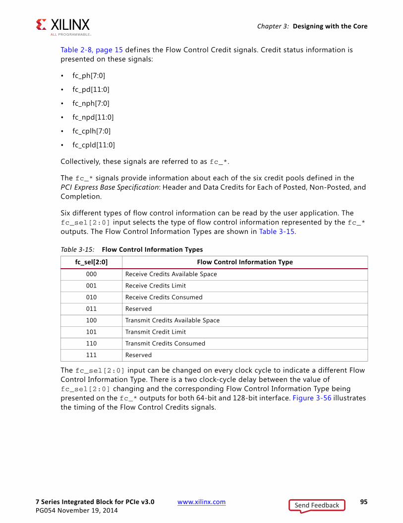
7 Series Integrated Block for PCIe v3.0 www.xilinx.com 95PG054 November 19, 2014
Chapter 3: Designing with the Core
Table 2-8, page 15 defines the Flow Control Credit signals. Credit status information is presented on these signals:
• fc_ph[7:0]
• fc_pd[11:0]
• fc_nph[7:0]
• fc_npd[11:0]
• fc_cplh[7:0]
• fc_cpld[11:0]
Collectively, these signals are referred to as fc_*.
The fc_* signals provide information about each of the six credit pools defined in the PCI Express Base Specification: Header and Data Credits for Each of Posted, Non-Posted, and Completion.
Six different types of flow control information can be read by the user application. The fc_sel[2:0] input selects the type of flow control information represented by the fc_* outputs. The Flow Control Information Types are shown in Table 3-15.
The fc_sel[2:0] input can be changed on every clock cycle to indicate a different Flow Control Information Type. There is a two clock-cycle delay between the value of fc_sel[2:0] changing and the corresponding Flow Control Information Type being presented on the fc_* outputs for both 64-bit and 128-bit interface. Figure 3-56 illustrates the timing of the Flow Control Credits signals.
Table 3-15: Flow Control Information Types
fc_sel[2:0] Flow Control Information Type
000 Receive Credits Available Space
001 Receive Credits Limit
010 Receive Credits Consumed
011 Reserved
100 Transmit Credits Available Space
101 Transmit Credit Limit
110 Transmit Credits Consumed
111 Reserved
Send Feedback
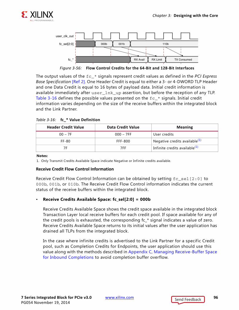
7 Series Integrated Block for PCIe v3.0 www.xilinx.com 96PG054 November 19, 2014
Chapter 3: Designing with the Core
The output values of the fc_* signals represent credit values as defined in the PCI Express Base Specification [Ref 2]. One Header Credit is equal to either a 3- or 4-DWORD TLP Header and one Data Credit is equal to 16 bytes of payload data. Initial credit information is available immediately after user_lnk_up assertion, but before the reception of any TLP. Table 3-16 defines the possible values presented on the fc_* signals. Initial credit information varies depending on the size of the receive buffers within the integrated block and the Link Partner.
Receive Credit Flow Control Information
Receive Credit Flow Control Information can be obtained by setting fc_sel[2:0] to 000b, 001b, or 010b. The Receive Credit Flow Control information indicates the current status of the receive buffers within the integrated block.
• Receive Credits Available Space: fc_sel[2:0] = 000b
Receive Credits Available Space shows the credit space available in the integrated block Transaction Layer local receive buffers for each credit pool. If space available for any of the credit pools is exhausted, the corresponding fc_* signal indicates a value of zero. Receive Credits Available Space returns to its initial values after the user application has drained all TLPs from the integrated block.
In the case where infinite credits is advertised to the Link Partner for a specific Credit pool, such as Completion Credits for Endpoints, the user application should use this value along with the methods described in Appendix C, Managing Receive-Buffer Space for Inbound Completions to avoid completion buffer overflow.
X-Ref Target - Figure 3-56
Figure 3-56: Flow Control Credits for the 64-Bit and 128-Bit Interfaces
Table 3-16: fc_* Value Definition
Header Credit Value Data Credit Value Meaning
00 – 7F 000 – 7FF User credits
FF-80 FFF-800 Negative credits available(1)
7F 7FF Infinite credits available(1)
Notes: 1. Only Transmit Credits Available Space indicate Negative or Infinite credits available.
user_clk_out
fc_sel[2:0]
fc_*
000b 001b 110b
RX Avail RX Limit TX Consumed
Send Feedback
7 Series Integrated Block for PCIe v3.0 www.xilinx.com 97PG054 November 19, 2014
Chapter 3: Designing with the Core
• Receive Credits Limit: fc_sel[2:0] = 001b
Receive Credits Limit shows the credits granted to the link partner. The fc_* values are initialized with the values advertised by the integrated block during Flow Control initialization and are updated as a cumulative count as TLPs are read out of the Transaction Layer receive buffers through the AXI4-Stream interface. This value is referred to as CREDITS_ALLOCATED within the PCI Express Base Specification.
In the case where infinite credits have been advertised for a specif ic credit pool, the Receive Buffer Credits Limit for that pool always indicates zero credits.
• Receive Credits Consumed: fc_sel[2:0] = 010b
Receive Buffer Credits Consumed shows the credits consumed by the link partner (and received by the integrated block). The initial fc_* values are always zero and are updated as a cumulative count, as packets are received by the Transaction Layers receive buffers. This value is referred to as CREDITS_RECEIVED in the PCI Express Base Specification.
Transmit Credit Flow Control Information
Transmit Credit Flow Control Information can be obtained by setting fc_sel[2:0] to 100b, 101b, or 110b. The Transmit Credit Flow Control information indicates the current status of the receive buffers within the Link Partner.
• Transmit Credits Available Space: fc_sel[2:0] = 100b
Transmit Credits Available Space indicates the available credit space within the receive buffers of the Link Partner for each credit pool. If space available for any of the credit pools is exhausted, the corresponding fc_* signal indicates a value of zero or negative. Transmit Credits Available Space returns to its initial values after the integrated block has successfully sent all TLPs to the Link Partner.
If the value is negative, more header or data has been written into the local transmit buffers of the integrated block than the Link Partner can currently consume. Because the block does not allow posted packets to pass completions, a posted packet that is written is not transmitted if there is a completion ahead of it waiting for credits (as indicated by a zero or negative value). Similarly, a completion that is written is not transmitted if a posted packet is ahead of it waiting for credits. The user application can monitor the Transmit Credits Available Space to ensure that these temporary blocking conditions do not occur, and that the bandwidth of the PCI Express Link is fully utilized by only writing packets to the integrated block that have suff icient space within the Receive buffer of the Link Partner. Non-Posted packets can always be bypassed within the integrated block; so, any Posted or Completion packet written passes Non-Posted packets waiting for credits.
The Link Partner can advertise infinite credits for one or more of the three traff ic types. Set the Header and Data credit outputs to their maximum value, as indicated in
Send Feedback
7 Series Integrated Block for PCIe v3.0 www.xilinx.com 98PG054 November 19, 2014
Chapter 3: Designing with the Core
Table 3-16, to indicate infinite credits.
• Transmit Credits Limit: fc_sel[2:0] = 101b
Transmit Credits Limit shows the receive buffer limits of the Link Partner for each credit pool. The fc_* values are initialized with the values advertised by the Link Partner during Flow Control initialization and are updated as a cumulative count as Flow Control updates are received from the Link Partner. This value is referred to as CREDITS_LIMIT in the PCI Express Base Specification [Ref 2].
In the case where infinite credits have been advertised for a specif ic Credit pool, the Transmit Buffer Credits Limit always indicates zero credits for that pool.
• Transmit Credits Consumed: fc_sel[2:0] = 110b
Transmit Credits Consumed show the credits consumed of the Receive Buffer of the Link Partner by the integrated block. The initial value is always zero and is updated as a cumulative count, as packets are transmitted to the Link Partner. This value is referred to as CREDITS_CONSUMED in the PCI Express Base Specification.
Designing with the Physical Layer Control and Status InterfacePhysical Layer Control and Status enables the user application to change link width and speed in response to data throughput and power requirements.
Design Considerations for a Directed Link Change
These points should be considered during a Directed Link Change:
• Link change operation must be initiated only when user_lnk_up is asserted and the core is in the L0 state, as indicated by the pl_ltssm_state[5:0] signal.
• Link Width Change should not be used when Lane Reversal is enabled.
• Target Link Width of a Link Width Change operation must be equal to or less than the width indicated by pl_initial_link_width output.
• When pl_link_upcfg_cap is set to 1b, the PCI Express link is Upconfigure capable. This allows the link width to be varied between the Initial Negotiated Link Width and any smaller link width supported by both the Port and link partner (this is for link reliability or application reasons).
• If a link is not Upconfigure capable, the Negotiated link width can only be varied to a width less than the Negotiated Link Width that is supported by both the link partner and device.
• Before initiating a link speed change from 2.5 Gb/s to 5.0 Gb/s, the user application must ensure that the link is 5.0 Gb/s (Gen2) capable (that is, pl_link_gen2_cap is 1b) and the Link Partner is also Gen2 capable (pl_link_partner_gen2_capable is 1b).
Send Feedback
7 Series Integrated Block for PCIe v3.0 www.xilinx.com 99PG054 November 19, 2014
Chapter 3: Designing with the Core
• A link width change that benefits the application must be initiated only when cfg_lcommand[9] (the Hardware Autonomous Width Disable bit) is 0b. In addition, for both link speed and/or width change driven by application need, pl_directed_link_auton must be driven (1b). To restore the link width and speed to the original (higher) width and speed, set pl_link_upcfg_cap to 1b.
• If the user application directs the link to a width not supported by the link partner, the resulting link width is the next narrower mutually supported link width. For example, an 8-lane link is directed to a 4-lane operation, but the link partner supports only 1-lane train down operations. So, this would result in a 1-lane operation.
• The Endpoint should initiate directed link change only when the device is in D0 power state (cfg_pmcsr_powerstate[1:0] = 00b).
• A retrain should not be initiated using directed link change pins (Root or Endpoint) or by setting the retrain bit (Root only), if the cfg_pcie_link_state = 101b (transitioning to/from PPM L1) or 110b (transitioning to PPM L2/L3 Ready).
• To ease timing closure, it is permitted to check for the conditions specif ied above to be all simultaneously TRUE up to 16 user clock cycles before initiating a Directed Link Change. These conditions are:
° user_lnk_up == 1'b1
° pl_ltssm_state[5:0] == 6'h16
° cfg_lcommand[9] == 1'b0
° cfg_pmcsr_powerstate[1:0] == 2'b00
° cfg_pcie_link_state[2:0] != either 3'b101 or 3'b110
Directed Link Width Change
Figure 3-57 shows the directed link width change process that must be implemented by the user application. Here target_link_width[1:0] is the application-driven new link width request.
Send Feedback
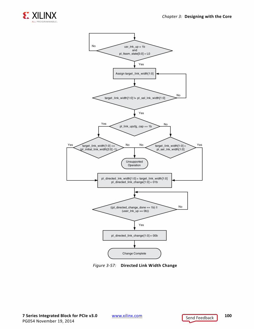
7 Series Integrated Block for PCIe v3.0 www.xilinx.com 100PG054 November 19, 2014
Chapter 3: Designing with the Core
X-Ref Target - Figure 3-57
Figure 3-57: Directed Link Width Change
target_link_width[1:0] != pl_sel_lnk_width[1:0]
Yes
Yes
pl_link_upcfg_cap == 1b
target_link_width[1:0] <= (pl_initial_link_width[2:0] -1)
target_link_width[1:0] < pl_sel_lnk_width[1:0]
Unsupported Operation
No No
pl_directed_lnk_width[1:0] = target_link_width[1:0]pl_directed_link_change[1:0] = 01b
Yes Yes
((pl_directed_change_done == 1b) ||(user_lnk_up == 0b))
No
pl_directed_link_change[1:0] = 00b
Change Complete
No
Assign target_link_width[1:0]
Yes
No
usr_lnk_up = 1band
pl_ltssm_state[5:0] = L0
Yes
No
Send Feedback
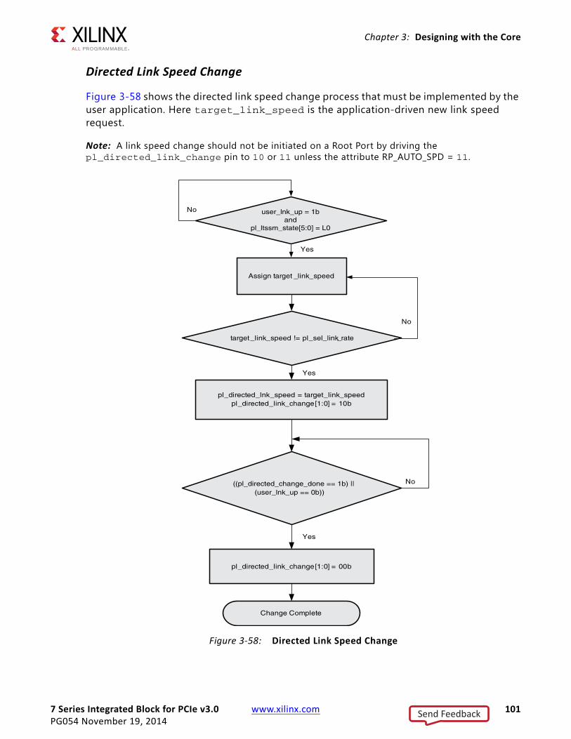
7 Series Integrated Block for PCIe v3.0 www.xilinx.com 101PG054 November 19, 2014
Chapter 3: Designing with the Core
Directed Link Speed Change
Figure 3-58 shows the directed link speed change process that must be implemented by the user application. Here target_link_speed is the application-driven new link speed request.
Note: A link speed change should not be initiated on a Root Port by driving the pl_directed_link_change pin to 10 or 11 unless the attribute RP_AUTO_SPD = 11.X-Ref Target - Figure 3-58
Figure 3-58: Directed Link Speed Change
target_link_speed != pl_sel_link_rate
No
Yes
pl_directed_lnk_speed = target_link_speedpl_directed_link_change[1:0] = 10b
((pl_directed_change_done == 1b) ||(user_lnk_up == 0b))
No
pl_directed_link_change[1:0] = 00b
Change Complete
Assign target _link_speed
Yes
Yes
No user_lnk_up = 1band
pl_ltssm_state[5:0] = L0
Send Feedback

7 Series Integrated Block for PCIe v3.0 www.xilinx.com 102PG054 November 19, 2014
Chapter 3: Designing with the Core
Directed Link Width and Speed Change
Figure 3-59 shows the directed link width and speed change process that must be implemented by the user application. Here target_link_width[1:0] is the application-driven new link width request, and target_link_speed is the application-driven new link speed request.
Note: A link speed change should not be initiated on a Root Port by driving the pl_directed_link_change pin to 10 or 11 unless the attribute RP_AUTO_SPD = 11.
Send Feedback

7 Series Integrated Block for PCIe v3.0 www.xilinx.com 103PG054 November 19, 2014
Chapter 3: Designing with the Core
X-Ref Target - Figure 3-59
Figure 3-59: Directed Link Width and Speed Change
(target_link_width[1:0] != pl_sel_lnk_width[1:0])&&
(target_link_speed != pl_sel_lnk_rate)
No
Yes
Yes
pl_link_upcfg_capable == 1b
target_link_width[1:0] <= (pl_initial_link_width[2:0] -1)
target_link_width[1:0] < pl_sel_lnk_width[1:0]
Unsupported Operation
No No
pl_directed_lnk_width[1:0] = target_link_width[1:0]pl_directed_lnk_speed = target_link_speed
pl_directed_link_change[1:0] = 11b
Yes Yes
((pl_directed_change_done == 1b) ||(user_lnk_up == 0b))
No
pl_directed_link_change[1:0] = 00b
Change Complete
No
Assign target_link_width[1:0]Assign target _link_speed
Yes
Yes
user_lnk_up = 1band
pl_ltssm_state[5:0] = L0
No
Send Feedback
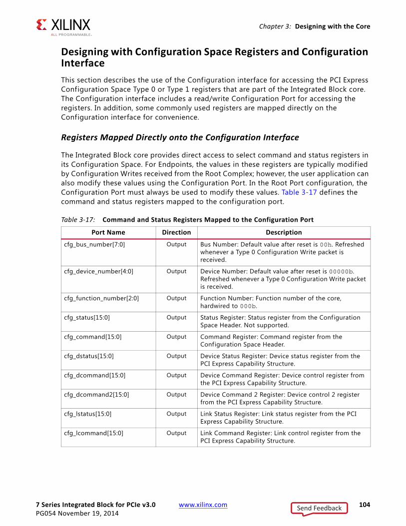
7 Series Integrated Block for PCIe v3.0 www.xilinx.com 104PG054 November 19, 2014
Chapter 3: Designing with the Core
Designing with Configuration Space Registers and Configuration InterfaceThis section describes the use of the Configuration interface for accessing the PCI Express Configuration Space Type 0 or Type 1 registers that are part of the Integrated Block core. The Configuration interface includes a read/write Configuration Port for accessing the registers. In addition, some commonly used registers are mapped directly on the Configuration interface for convenience.
Registers Mapped Directly onto the Configuration Interface
The Integrated Block core provides direct access to select command and status registers in its Configuration Space. For Endpoints, the values in these registers are typically modif ied by Configuration Writes received from the Root Complex; however, the user application can also modify these values using the Configuration Port. In the Root Port configuration, the Configuration Port must always be used to modify these values. Table 3-17 defines the command and status registers mapped to the configuration port.
Table 3-17: Command and Status Registers Mapped to the Configuration Port
Port Name Direction Description
cfg_bus_number[7:0] Output Bus Number: Default value after reset is 00h. Refreshed whenever a Type 0 Configuration Write packet is received.
cfg_device_number[4:0] Output Device Number: Default value after reset is 00000b. Refreshed whenever a Type 0 Configuration Write packet is received.
cfg_function_number[2:0] Output Function Number: Function number of the core, hardwired to 000b.
cfg_status[15:0] Output Status Register: Status register from the Configuration Space Header. Not supported.
cfg_command[15:0] Output Command Register: Command register from the Configuration Space Header.
cfg_dstatus[15:0] Output Device Status Register: Device status register from the PCI Express Capability Structure.
cfg_dcommand[15:0] Output Device Command Register: Device control register from the PCI Express Capability Structure.
cfg_dcommand2[15:0] Output Device Command 2 Register: Device control 2 register from the PCI Express Capability Structure.
cfg_lstatus[15:0] Output Link Status Register: Link status register from the PCI Express Capability Structure.
cfg_lcommand[15:0] Output Link Command Register: Link control register from the PCI Express Capability Structure.
Send Feedback
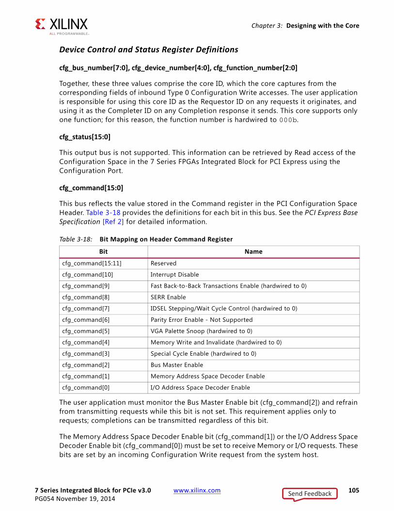
7 Series Integrated Block for PCIe v3.0 www.xilinx.com 105PG054 November 19, 2014
Chapter 3: Designing with the Core
Device Control and Status Register Definitions
cfg_bus_number[7:0], cfg_device_number[4:0], cfg_function_number[2:0]
Together, these three values comprise the core ID, which the core captures from the corresponding f ields of inbound Type 0 Configuration Write accesses. The user application is responsible for using this core ID as the Requestor ID on any requests it originates, and using it as the Completer ID on any Completion response it sends. This core supports only one function; for this reason, the function number is hardwired to 000b.
cfg_status[15:0]
This output bus is not supported. This information can be retrieved by Read access of the Configuration Space in the 7 Series FPGAs Integrated Block for PCI Express using the Configuration Port.
cfg_command[15:0]
This bus reflects the value stored in the Command register in the PCI Configuration Space Header. Table 3-18 provides the definitions for each bit in this bus. See the PCI Express Base Specification [Ref 2] for detailed information.
The user application must monitor the Bus Master Enable bit (cfg_command[2]) and refrain from transmitting requests while this bit is not set. This requirement applies only to requests; completions can be transmitted regardless of this bit.
The Memory Address Space Decoder Enable bit (cfg_command[1]) or the I/O Address Space Decoder Enable bit (cfg_command[0]) must be set to receive Memory or I/O requests. These bits are set by an incoming Configuration Write request from the system host.
Table 3-18: Bit Mapping on Header Command Register
Bit Name
cfg_command[15:11] Reserved
cfg_command[10] Interrupt Disable
cfg_command[9] Fast Back-to-Back Transactions Enable (hardwired to 0)
cfg_command[8] SERR Enable
cfg_command[7] IDSEL Stepping/Wait Cycle Control (hardwired to 0)
cfg_command[6] Parity Error Enable - Not Supported
cfg_command[5] VGA Palette Snoop (hardwired to 0)
cfg_command[4] Memory Write and Invalidate (hardwired to 0)
cfg_command[3] Special Cycle Enable (hardwired to 0)
cfg_command[2] Bus Master Enable
cfg_command[1] Memory Address Space Decoder Enable
cfg_command[0] I/O Address Space Decoder Enable
Send Feedback

7 Series Integrated Block for PCIe v3.0 www.xilinx.com 106PG054 November 19, 2014
Chapter 3: Designing with the Core
cfg_dstatus[15:0]
This bus reflects the value stored in the Device Status register of the PCI Express Capabilities Structure. Table 3-19 defines each bit in the cfg_dstatus bus. See the PCI Express Base Specification [Ref 2] for detailed information.
cfg_dcommand[15:0]
This bus reflects the value stored in the Device Control register of the PCI Express Capabilities Structure. Table 3-20 defines each bit in the cfg_dcommand bus. See the PCI Express Base Specification for detailed information.
cfg_lstatus[15:0]
This bus reflects the value stored in the Link Status register in the PCI Express Capabilities Structure. Table 3-21 defines each bit in the cfg_lstatus bus. See the PCI Express Base Specification for details.
Table 3-19: Bit Mapping on PCI Express Device Status Register
Bit Name
cfg_dstatus[15:6] Reserved
cfg_dstatus[5] Transaction Pending
cfg_dstatus[4] AUX Power Detected (hardwired to 0)
cfg_dstatus[3] Unsupported Request Detected
cfg_dstatus[2] Fatal Error Detected
cfg_dstatus[1] Non-Fatal Error Detected
cfg_dstatus[0] Correctable Error Detected
Table 3-20: Bit Mapping of PCI Express Device Control Register
Bit Name
cfg_dcommand[15] Reserved
cfg_dcommand[14:12] Max_Read_Request_Size
cfg_dcommand[11] Enable No Snoop
cfg_dcommand[10] Auxiliary Power PM Enable
cfg_dcommand[9] Phantom Functions Enable
cfg_dcommand[8] Extended Tag Field Enable
cfg_dcommand[7:5] Max_Payload_Size
cfg_dcommand[4] Enable Relaxed Ordering
cfg_dcommand[3] Unsupported Request Reporting Enable
cfg_dcommand[2] Fatal Error Reporting Enable
cfg_dcommand[1] Non-Fatal Error Reporting Enable
cfg_dcommand[0] Correctable Error Reporting Enable
Send Feedback
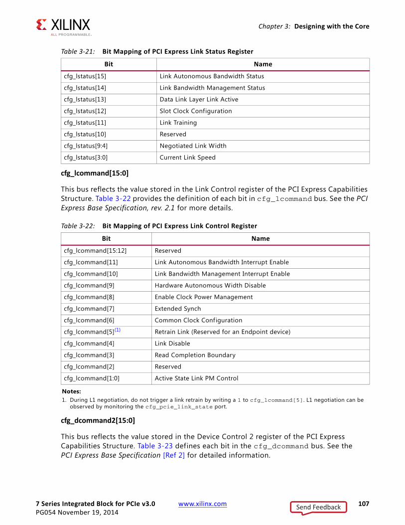
7 Series Integrated Block for PCIe v3.0 www.xilinx.com 107PG054 November 19, 2014
Chapter 3: Designing with the Core
cfg_lcommand[15:0]
This bus reflects the value stored in the Link Control register of the PCI Express Capabilities Structure. Table 3-22 provides the definition of each bit in cfg_lcommand bus. See the PCI Express Base Specification, rev. 2.1 for more details.
cfg_dcommand2[15:0]
This bus reflects the value stored in the Device Control 2 register of the PCI Express Capabilities Structure. Table 3-23 defines each bit in the cfg_dcommand bus. See the PCI Express Base Specification [Ref 2] for detailed information.
Table 3-21: Bit Mapping of PCI Express Link Status Register
Bit Name
cfg_lstatus[15] Link Autonomous Bandwidth Status
cfg_lstatus[14] Link Bandwidth Management Status
cfg_lstatus[13] Data Link Layer Link Active
cfg_lstatus[12] Slot Clock Configuration
cfg_lstatus[11] Link Training
cfg_lstatus[10] Reserved
cfg_lstatus[9:4] Negotiated Link Width
cfg_lstatus[3:0] Current Link Speed
Table 3-22: Bit Mapping of PCI Express Link Control Register
Bit Name
cfg_lcommand[15:12] Reserved
cfg_lcommand[11] Link Autonomous Bandwidth Interrupt Enable
cfg_lcommand[10] Link Bandwidth Management Interrupt Enable
cfg_lcommand[9] Hardware Autonomous Width Disable
cfg_lcommand[8] Enable Clock Power Management
cfg_lcommand[7] Extended Synch
cfg_lcommand[6] Common Clock Configuration
cfg_lcommand[5](1) Retrain Link (Reserved for an Endpoint device)
cfg_lcommand[4] Link Disable
cfg_lcommand[3] Read Completion Boundary
cfg_lcommand[2] Reserved
cfg_lcommand[1:0] Active State Link PM Control
Notes: 1. During L1 negotiation, do not trigger a link retrain by writing a 1 to cfg_lcommand[5]. L1 negotiation can be
observed by monitoring the cfg_pcie_link_state port.
Send Feedback

7 Series Integrated Block for PCIe v3.0 www.xilinx.com 108PG054 November 19, 2014
Chapter 3: Designing with the Core
Core Response to Command Register Settings
Table 3-24 and Table 3-25 illustrate the behavior of the core based on the Command Register settings when configured as either an Endpoint or a Root Port.
Table 3-23: Bit Mapping of PCI Express Device Control 2 Register
Bit Name
cfg_dcommand2[15:5] Reserved
cfg_dcommand2[4] Completion Timeout Disable
cfg_dcommand2[3:0] Completion Timeout Value
Table 3-24: Command Register (0x004): Endpoint
Bit Name Attr Endpoint Core Behavior
0 I/O Space Enable RW The Endpoint does not permit a BAR hit on I/O space unless this is enabled.
1 Memory Space Enable RW The Endpoint does not permit a BAR hit on Memory space unless this is enabled.
2 Bus Master Enable RW The Endpoint does not enforce this; user could send a TLP through the AXI4-Stream interface.
5:3 Reserved RO Wired to 0. Not applicable to PCI Express.
6 Parity Error Response RW Enables Master Data Parity Error (Status[8]) to be set.
7 Reserved RO Wired to 0. Not applicable to PCI Express.
8 SERR# Enable RW Can enable Error NonFatal / Error Fatal Message generation, and enables Status[14] (“Signaled System Error”).
9 Reserved RO Wired to 0. Not applicable to PCI Express.
10 Interrupt Disable RW If set to 1, the cfg_interrupt* interface is unable to cause INTx messages to be sent.
15:11 Reserved RO Wired to 0. Not applicable to PCI Express.
Table 3-25: Command Register (0x004): Root Port
Bit Name Attr Root Port Core behavior
0 I/O Space Enable RW The Root Port ignores this setting. If disabled, it still accepts I/O TLP from the user side and passes downstream. The user application logic must enforce not sending I/O TLPs downstream if this is unset.
1 Memory Space Enable RW The Root Port ignores this setting. If disabled, it still accepts Mem TLPs from the user side and passes downstream. The user application logic must enforce not sending Mem TLPs downstream if this is unset.
Send Feedback
7 Series Integrated Block for PCIe v3.0 www.xilinx.com 109PG054 November 19, 2014
Chapter 3: Designing with the Core
Status Register Response to Error Conditions
Table 3-26 throughTable 3-28 illustrate the conditions that cause the Status Register bits to be set in the core when configured as either an Endpoint or a Root Port.
2 Bus Master Enable RW When set to 0, the Root Port responds to target transactions such as an Upstream Mem or I/O TLPs as a UR (that is, the UR bit is set if enabled or a Cpl w/ UR packet is sent if the TLP was Non-Posted). When set to 1, all target transactions are passed to the user.
5:3 Reserved RO Wired to 0. Not applicable to PCI Express.
6 Parity Error Response RW Enables Master Data Parity Error (Status[8]) to be set.
7 Reserved RO Wired to 0. Not applicable to PCI Express.
8 SERR# Enable RW If enabled, Error Fatal/Error Non-Fatal Messages can be forwarded from the AXI4-Stream interface or cfg_err*, or internally generated. The Root Port does not enforce the requirement that Error Fatal/Error Non-Fatal Messages received on the link not be forwarded if this bit is unset; instead, the user logic must do that. Note: Error conditions detected internal to the Root Port are indicated on cfg_msg* interface.
9 Reserved RO Wired to 0. Not applicable to PCI Express.
10 Interrupt Disable RW Not applicable to Root Port.
15:11 Reserved RO Wired to 0. Not applicable to PCI Express.
Table 3-26: Status Register (0x006): Endpoint
Bit Name Attr Cause in an Endpoint
2:0 Reserved RO Wired to 0. Not applicable to PCI Express.
3 Interrupt Status RO • Set when interrupt signaled by user.• Clears when interrupt is cleared by the Interrupt
handler.
4 Capabilities List RO Wired to 1.
7:5 Reserved RO Wired to 0. Not applicable to PCI Express.
8 Master Data Parity Error RW1C Set if Parity Error Response is set and a Poisoned Cpl TLP is received on the link, or a Poisoned Write TLP is sent.
10:9 Reserved RO Wired to 0. Not applicable to PCI Express.
11 Signaled Target Abort RW1C Set if a Completion with status Completer Abort is sent upstream by the user application through the cfg_err* interface.
12 Received Target Abort RW1C Set if a Completion with status Completer Abort is received.
Table 3-25: Command Register (0x004): Root Port (Cont’d)
Bit Name Attr Root Port Core behavior
Send Feedback

7 Series Integrated Block for PCIe v3.0 www.xilinx.com 110PG054 November 19, 2014
Chapter 3: Designing with the Core
13 Received Master Abort RW1C Set if a Completion with status Unsupported Request is received.
14 Signaled System Error RW1C Set if an Error Non-Fatal / Error Fatal Message is sent, and SERR# Enable (Command[8]) is set.
15 Detected Parity Error RW1C Set if a Poisoned TLP is received on the link.
Table 3-27: Status Register (0x006): Root Port
Bit Name Attr Cause in a Root Port
2:0 Reserved RO Wired to 0. Not applicable to PCI Express.
3 Interrupt Status RO Has no function in the Root Port.
4 Capabilities List RO Wired to 1.
7:5 Reserved RO Wired to 0. Not applicable to PCI Express.
8 Master Data Parity Error RW1C Set if Parity Error Response is set and a Poisoned Completion TLP is received on the link.
10:9 Reserved RO Wired to 0. Not applicable to PCI Express.
11 Signaled Target Abort RW1C Never set by the Root Port
12 Received Target Abort RW1C Never set by the Root Port
13 Received Master Abort RW1C Never set by the Root Port
14 Signaled System Error RW1C Set if the Root Port:• Receives an Error Non-Fatal / Error Fatal Message and
both SERR# Enable and Secondary SERR# enable are set.
• Indicates on the cfg_msg* interface that a Error Fatal / Error Non-Fatal Message should be generated upstream and SERR# enable is set.
15 Detected Parity Error RW1C Set if a Poisoned TLP is transmitted downstream.
Table 3-28: Secondary Status Register (0x01E): Root Port
Bit Name Attr Cause in a Root Port
7:0 Reserved RO Wired to 0. Not applicable to PCI Express.
8 Secondary Master Data Parity Error RW1C Set when the Root Port:Receives a Poisoned Completion TLP, and Secondary Parity Error Response==1 Transmits a Poisoned Write TLP, and Secondary Parity Error Response==1
10:9 Reserved RO Wired to 0. Not applicable to PCI Express.
Table 3-26: Status Register (0x006): Endpoint (Cont’d)
Bit Name Attr Cause in an Endpoint
Send Feedback
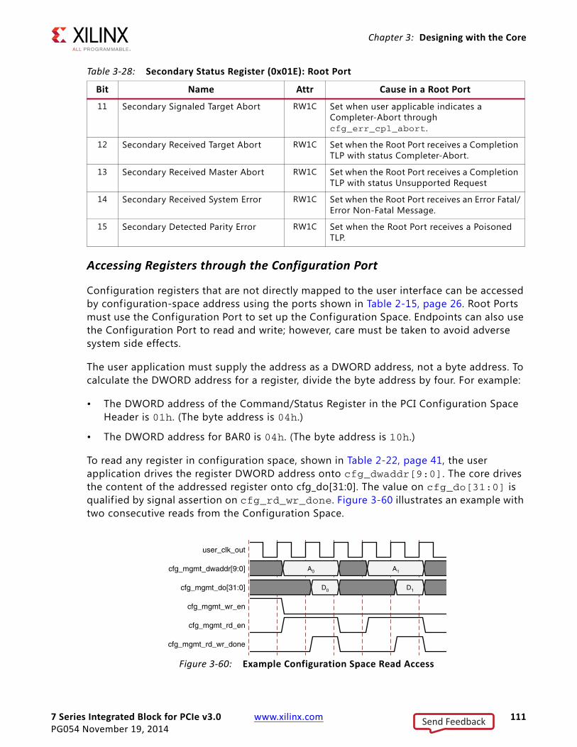
7 Series Integrated Block for PCIe v3.0 www.xilinx.com 111PG054 November 19, 2014
Chapter 3: Designing with the Core
Accessing Registers through the Configuration Port
Configuration registers that are not directly mapped to the user interface can be accessed by configuration-space address using the ports shown in Table 2-15, page 26. Root Ports must use the Configuration Port to set up the Configuration Space. Endpoints can also use the Configuration Port to read and write; however, care must be taken to avoid adverse system side effects.
The user application must supply the address as a DWORD address, not a byte address. To calculate the DWORD address for a register, divide the byte address by four. For example:
• The DWORD address of the Command/Status Register in the PCI Configuration Space Header is 01h. (The byte address is 04h.)
• The DWORD address for BAR0 is 04h. (The byte address is 10h.)
To read any register in configuration space, shown in Table 2-22, page 41, the user application drives the register DWORD address onto cfg_dwaddr[9:0]. The core drives the content of the addressed register onto cfg_do[31:0]. The value on cfg_do[31:0] is qualif ied by signal assertion on cfg_rd_wr_done. Figure 3-60 illustrates an example with two consecutive reads from the Configuration Space.
11 Secondary Signaled Target Abort RW1C Set when user applicable indicates a Completer-Abort through cfg_err_cpl_abort.
12 Secondary Received Target Abort RW1C Set when the Root Port receives a Completion TLP with status Completer-Abort.
13 Secondary Received Master Abort RW1C Set when the Root Port receives a Completion TLP with status Unsupported Request
14 Secondary Received System Error RW1C Set when the Root Port receives an Error Fatal/Error Non-Fatal Message.
15 Secondary Detected Parity Error RW1C Set when the Root Port receives a Poisoned TLP.
X-Ref Target - Figure 3-60
Figure 3-60: Example Configuration Space Read Access
Table 3-28: Secondary Status Register (0x01E): Root Port
Bit Name Attr Cause in a Root Port
user_clk_out
cfg_mgmt_dwaddr[9:0]
cfg_mgmt_do[31:0]
cfg_mgmt_wr_en
cfg_mgmt_rd_en
cfg_mgmt_rd_wr_done
A0 A1
D0 D1
Send Feedback
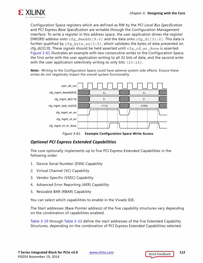
7 Series Integrated Block for PCIe v3.0 www.xilinx.com 112PG054 November 19, 2014
Chapter 3: Designing with the Core
Configuration Space registers which are defined as RW by the PCI Local Bus Specification and PCI Express Base Specification are writable through the Configuration Management interface. To write a register in this address space, the user application drives the register DWORD address onto cfg_dwaddr[9:0] and the data onto cfg_di[31:0]. This data is further qualif ied by cfg_byte_en[3:0], which validates the bytes of data presented on cfg_di[31:0]. These signals should be held asserted until cfg_rd_wr_done is asserted. Figure 3-61 illustrates an example with two consecutive writes to the Configuration Space, the first write with the user application writing to all 32 bits of data, and the second write with the user application selectively writing to only bits [23:16].
Note: Writing to the Configuration Space could have adverse system side effects. Ensure these writes do not negatively impact the overall system functionality.
Optional PCI Express Extended Capabilities
The core optionally implements up to f ive PCI Express Extended Capabilities in the following order:
1. Device Serial Number (DSN) Capability
2. Virtual Channel (VC) Capability
3. Vendor Specif ic (VSEC) Capability
4. Advanced Error Reporting (AER) Capability
5. Resizable BAR (RBAR) Capability
You can select which capabilities to enable in the Vivado IDE.
The Start addresses (Base Pointer address) of the f ive capability structures vary depending on the combination of capabilities enabled.
Table 3-29 through Table 3-33 define the start addresses of the f ive Extended Capability Structures, depending on the combination of PCI Express Extended Capabilities selected.
X-Ref Target - Figure 3-61
Figure 3-61: Example Configuration Space Write Access
user_clk_out
cfg_mgmt_dwaddr[9:0]
cfg_mgmt_di[31:0]
cfg_mgmt_byte_en[3:0]
cfg_mgmt_wr_en
cfg_mgmt_rd_en
cfg_mgmt_rd_wr_done
A A
D
0
D
1
1111b 0100b
Send Feedback
7 Series Integrated Block for PCIe v3.0 www.xilinx.com 113PG054 November 19, 2014
Chapter 3: Designing with the Core
Table 3-29: DSN Base Pointer
DSN Base Pointer
No Capabilities Selected -
DSN Enabled 100h
Table 3-30: VC Capability Base Pointer
VC Capability Base Pointer
No Capabilities Selected -
Only VC Capability Enabled 100h
DSN and VC Capability Enabled 10Ch
Table 3-31: VSEC Capability Base Pointer
VSEC Capability Base Pointer
No Capabilities Selected -
Only VSEC Capability Enabled 100h
DSN and VSEC Capability Enabled 10Ch
DSN, VC Capability, and VSEC Capability Enabled 128h
Table 3-32: AER Capability Base Pointer
AER Capability Base Pointer
No Capabilities Selected -
Only AER Capability Enabled 100h
DSN and AER Capability Enabled 10Ch
VC Capability and AER Capability Enabled 11Ch
VSEC Capability and AER Capability Enabled 118h
DSN, VC Capability, and AER Capability Enabled 128h
DSN, VSEC Capability, and AER Capability Enabled 124h
VC Capability, VSEC Capability, and AER Capability Enabled 134h
DSN, VC Capability, VSEC Capability, and AER Capability Enabled 140h
Table 3-33: RBAR Capability Base Pointer
RBAR Capability Base Pointer
No Capabilities Selected -
Only RBAR Capability Enabled 100h
DSN and RBAR Capability Enabled 10Ch
VC Capability and RBAR Capability Enabled 11Ch
VSEC Capability and RBAR Capability Enabled 118h
AER Capability and RBAR Capability Enabled 138h
Send Feedback
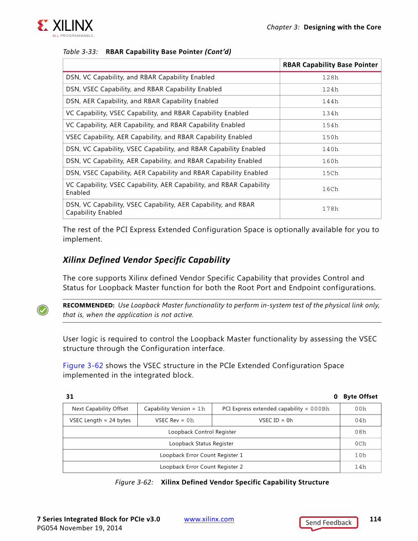
7 Series Integrated Block for PCIe v3.0 www.xilinx.com 114PG054 November 19, 2014
Chapter 3: Designing with the Core
The rest of the PCI Express Extended Configuration Space is optionally available for you to implement.
Xilinx Defined Vendor Specific Capability
The core supports Xilinx defined Vendor Specif ic Capability that provides Control and Status for Loopback Master function for both the Root Port and Endpoint configurations.
RECOMMENDED: Use Loopback Master functionality to perform in-system test of the physical link only, that is, when the application is not active.
User logic is required to control the Loopback Master functionality by assessing the VSEC structure through the Configuration interface.
Figure 3-62 shows the VSEC structure in the PCIe Extended Configuration Space implemented in the integrated block.
X-Ref Target - Figure 3-62
Figure 3-62: Xilinx Defined Vendor Specific Capability Structure
DSN, VC Capability, and RBAR Capability Enabled 128h
DSN, VSEC Capability, and RBAR Capability Enabled 124h
DSN, AER Capability, and RBAR Capability Enabled 144h
VC Capability, VSEC Capability, and RBAR Capability Enabled 134h
VC Capability, AER Capability, and RBAR Capability Enabled 154h
VSEC Capability, AER Capability, and RBAR Capability Enabled 150h
DSN, VC Capability, VSEC Capability, and RBAR Capability Enabled 140h
DSN, VC Capability, AER Capability, and RBAR Capability Enabled 160h
DSN, VSEC Capability, AER Capability and RBAR Capability Enabled 15Ch
VC Capability, VSEC Capability, AER Capability, and RBAR Capability Enabled 16Ch
DSN, VC Capability, VSEC Capability, AER Capability, and RBAR Capability Enabled 178h
Table 3-33: RBAR Capability Base Pointer (Cont’d)
RBAR Capability Base Pointer
31 0 Byte Offset
Next Capability Offset Capability Version = 1h PCI Express extended capability = 000Bh 00h
VSEC Length = 24 bytes VSEC Rev = 0h VSEC ID = 0h 04h
Loopback Control Register 08h
Loopback Status Register 0Ch
Loopback Error Count Register 1 10h
Loopback Error Count Register 2 14h
Send Feedback
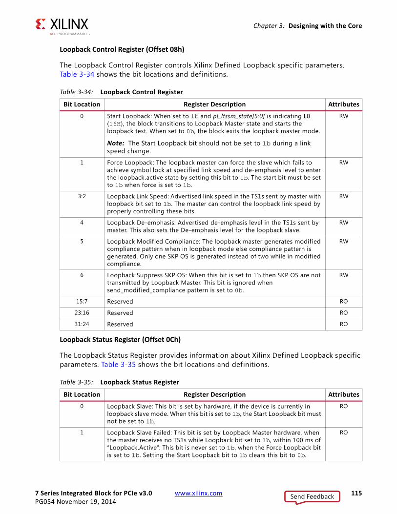
7 Series Integrated Block for PCIe v3.0 www.xilinx.com 115PG054 November 19, 2014
Chapter 3: Designing with the Core
Loopback Control Register (Offset 08h)
The Loopback Control Register controls Xilinx Defined Loopback specif ic parameters. Table 3-34 shows the bit locations and definitions.
Loopback Status Register (Offset 0Ch)
The Loopback Status Register provides information about Xilinx Defined Loopback specif ic parameters. Table 3-35 shows the bit locations and definitions.
Table 3-34: Loopback Control Register
Bit Location Register Description Attributes
0 Start Loopback: When set to 1b and pl_ltssm_state[5:0] is indicating L0 (16H), the block transitions to Loopback Master state and starts the loopback test. When set to 0b, the block exits the loopback master mode.
Note: The Start Loopback bit should not be set to 1b during a link speed change.
RW
1 Force Loopback: The loopback master can force the slave which fails to achieve symbol lock at specified link speed and de-emphasis level to enter the loopback.active state by setting this bit to 1b. The start bit must be set to 1b when force is set to 1b.
RW
3:2 Loopback Link Speed: Advertised link speed in the TS1s sent by master with loopback bit set to 1b. The master can control the loopback link speed by properly controlling these bits.
RW
4 Loopback De-emphasis: Advertised de-emphasis level in the TS1s sent by master. This also sets the De-emphasis level for the loopback slave.
RW
5 Loopback Modified Compliance: The loopback master generates modified compliance pattern when in loopback mode else compliance pattern is generated. Only one SKP OS is generated instead of two while in modif ied compliance.
RW
6 Loopback Suppress SKP OS: When this bit is set to 1b then SKP OS are not transmitted by Loopback Master. This bit is ignored when send_modif ied_compliance pattern is set to 0b.
RW
15:7 Reserved RO
23:16 Reserved RO
31:24 Reserved RO
Table 3-35: Loopback Status Register
Bit Location Register Description Attributes
0 Loopback Slave: This bit is set by hardware, if the device is currently in loopback slave mode. When this bit is set to 1b, the Start Loopback bit must not be set to 1b.
RO
1 Loopback Slave Failed: This bit is set by Loopback Master hardware, when the master receives no TS1s while Loopback bit set to 1b, within 100 ms of “Loopback.Active”. This bit is never set to 1b, when the Force Loopback bit is set to 1b. Setting the Start Loopback bit to 1b clears this bit to 0b.
RO
Send Feedback
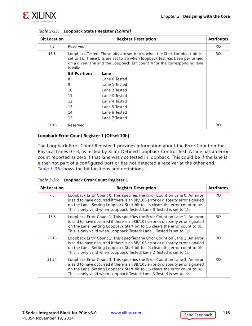
7 Series Integrated Block for PCIe v3.0 www.xilinx.com 116PG054 November 19, 2014
Chapter 3: Designing with the Core
Loopback Error Count Register 1 (Offset 10h)
The Loopback Error Count Register 1 provides information about the Error Count on the Physical Lanes 0 - 3, as tested by Xilinx Defined Loopback Control Test. A lane has an error count reported as zero if that lane was not tested in loopback. This could be if the lane is either not part of a configured port or has not detected a receiver at the other end. Table 3-36 shows the bit locations and definitions.
7:2 Reserved RO
15:8 Loopback Tested: These bits are set to 0b, when the Start Loopback bit is set to 1b. These bits are set to 1b when loopback test has been performed on a given lane and the Loopback_Err_count_n for the corresponding lane is valid.Bit Positions Lane8 Lane 0 Tested 9 Lane 1 Tested 10 Lane 2 Tested 11 Lane 3 Tested 12 Lane 4 Tested 13 Lane 5 Tested 14 Lane 6 Tested 15 Lane 7 Tested
RO
31:16 Reserved RO
Table 3-36: Loopback Error Count Register 1
Bit Location Register Description Attributes
7:0 Loopback Error Count 0: This specif ies the Error Count on Lane 0. An error is said to have occurred if there is an 8B/10B error or disparity error signaled on the Lane. Setting Loopback Start bit to 1b clears the error count to 0h. This is only valid when Loopback Tested: Lane 0 Tested is set to 1b.
RO
15:8 Loopback Error Count 1: This specif ies the Error Count on Lane 1. An error is said to have occurred if there is an 8B/10B error or disparity error signaled on the Lane. Setting Loopback Start bit to 1b clears the error count to 0h. This is only valid when Loopback Tested: Lane 1 Tested is set to 1b.
RO
23:16 Loopback Error Count 2: This specif ies the Error Count on Lane 2. An error is said to have occurred if there is an 8B/10B error or disparity error signaled on the Lane. Setting Loopback Start bit to 1b clears the error count to 0h. This is only valid when Loopback Tested: Lane 2 Tested is set to 1b.
RO
31:24 Loopback Error Count 3: This specif ies the Error Count on Lane 3. An error is said to have occurred if there is an 8B/10B error or disparity error signaled on the Lane. Setting Loopback Start bit to 1b clears the error count to 0h. This is only valid when Loopback Tested: Lane 3 Tested is set to 1b.
RO
Table 3-35: Loopback Status Register (Cont’d)
Bit Location Register Description Attributes
Send Feedback
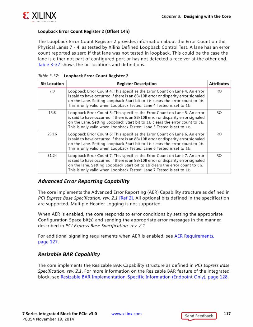
7 Series Integrated Block for PCIe v3.0 www.xilinx.com 117PG054 November 19, 2014
Chapter 3: Designing with the Core
Loopback Error Count Register 2 (Offset 14h)
The Loopback Error Count Register 2 provides information about the Error Count on the Physical Lanes 7 - 4, as tested by Xilinx Defined Loopback Control Test. A lane has an error count reported as zero if that lane was not tested in loopback. This could be the case the lane is either not part of configured port or has not detected a receiver at the other end. Table 3-37 shows the bit locations and definitions.
Advanced Error Reporting Capability
The core implements the Advanced Error Reporting (AER) Capability structure as defined in PCI Express Base Specification, rev. 2.1 [Ref 2]. All optional bits defined in the specification are supported. Multiple Header Logging is not supported.
When AER is enabled, the core responds to error conditions by setting the appropriate Configuration Space bit(s) and sending the appropriate error messages in the manner described in PCI Express Base Specification, rev. 2.1.
For additional signaling requirements when AER is enabled, see AER Requirements, page 127.
Resizable BAR Capability
The core implements the Resizable BAR Capability structure as defined in PCI Express Base Specification, rev. 2.1. For more information on the Resizable BAR feature of the integrated block, see Resizable BAR Implementation-Specif ic Information (Endpoint Only), page 128.
Table 3-37: Loopback Error Count Register 2
Bit Location Register Description Attributes
7:0 Loopback Error Count 4: This specif ies the Error Count on Lane 4. An error is said to have occurred if there is an 8B/10B error or disparity error signaled on the Lane. Setting Loopback Start bit to 1b clears the error count to 0h. This is only valid when Loopback Tested: Lane 4 Tested is set to 1b.
RO
15:8 Loopback Error Count 5: This specif ies the Error Count on Lane 5. An error is said to have occurred if there is an 8B/10B error or disparity error signaled on the Lane. Setting Loopback Start bit to 1b clears the error count to 0h. This is only valid when Loopback Tested: Lane 5 Tested is set to 1b.
RO
23:16 Loopback Error Count 6: This specif ies the Error Count on Lane 6. An error is said to have occurred if there is an 8B/10B error or disparity error signaled on the Lane. Setting Loopback Start bit to 1b clears the error count to 0h. This is only valid when Loopback Tested: Lane 6 Tested is set to 1b.
RO
31:24 Loopback Error Count 7: This specif ies the Error Count on Lane 7. An error is said to have occurred if there is an 8B/10B error or disparity error signaled on the lane. Setting Loopback Start bit to 1b clears the error count to 0h. This is only valid when Loopback Tested: Lane 7 Tested is set to 1b.
RO
Send Feedback

7 Series Integrated Block for PCIe v3.0 www.xilinx.com 118PG054 November 19, 2014
Chapter 3: Designing with the Core
User-Implemented Configuration Space
The core enables you to optionally implement registers in the PCI Configuration Space, the PCI Express Extended Configuration Space, or both, in the user application. The user application must return Config Completions for all address within this space. For more information about enabling and customizing this feature, see Chapter 4, Customizing and Generating the Core.
PCI Configuration Space
If you choose to implement registers within 0xA8 to 0xFF in the PCI Configuration Space, the start address of the address region you wish to implement can be defined during the core generation process.
The user application is responsible for generating all Completions to Configuration Reads and Writes from the user-defined start address to the end of PCI Configuration Space (0xFF). Configuration Reads to unimplemented registers within this range should be responded to with a Completion with 0x00000000 as the data, and configuration writes should be responded to with a successful Completion.
For example, to implement address range 0xC0 to 0xCF, there are several address ranges defined that should be treated differently depending on the access. See Table 3-38 for more details on this example.
PCI Express Extended Configuration Space
The starting address of the region in the PCI Express Extended Configuration Space that is optionally available for you to implement depends on the PCI Express Extended Capabilities that you enabled in the core.
The core allows you to select the start address of the user-implemented PCI Express Extended Configuration Space, while generating and customizing the core. This space must be implemented in the user application. The user application is required to generate a Cpld with 0x00000000 for Configuration Read and successful Cpl for Configuration Write to addresses in this selected range not implemented in the user application.
You can choose to implement a User Configuration Space with a start address not adjacent to the last capability structure implemented by the core. In such a case, the core returns a completion with 0x00000000 for configuration accesses to the region that you have
Table 3-38: Example: User-Implemented Space 0xC0 to 0xCF
Address Range Configuration Writes Configuration Reads
0x00 to 0xBF The core responds automatically The core responds automatically
0xC0 to 0xCF The user application responds with Successful Completion
The user application responds with register contents
0xD0 to 0xFF The user application responds with Successful Completion
The user application responds with 0x00000000
Send Feedback

7 Series Integrated Block for PCIe v3.0 www.xilinx.com 119PG054 November 19, 2014
Chapter 3: Designing with the Core
chosen to not implement. Table 3-39 further illustrates this scenario.
Table 3-39 illustrates an example Configuration of the PCI Express Extended Configuration Space, with these settings:
• DSN Capability Enabled
• VSEC Capability Enabled
• User Implemented PCI Express Extended Configuration Space Enabled
• User Implemented PCI Express Extended Configuration Space Start Address 168h
In this configuration, the DSN Capability occupies the registers at 100h-108h, and the VSEC Capability occupies registers at addresses 10Ch to 120h.
The remaining PCI Express Extended Configuration Space, starting at address 124h is available to implement. For this example, registers in the address region starting 168h were chosen for implement. The core returns successful completions with 0x00000000 for Configuration accesses to registers 124h-164h. Table 3-39 also illustrates a case where only registers from 168h to 47Ch are implemented. In this case, you are responsible for returning successful Completions with 0x00000000 for configuration accesses to 480h-FFFh.
Additional Packet Handling Requirements
The user application must manage the mechanisms described in this section to ensure protocol compliance, because the core does not manage them automatically.
Generation of Completions
The core does not generate Completions for Memory Reads or I/O requests made by a remote device. You must service these completions according to the rules specif ied in the PCI Express Base Specification [Ref 2].
Table 3-39: Example: User-Defined Start Address for Configuration Space
Configuration Space Byte Address
DSN Capability 100h - 108h
VSEC Capability 10Ch - 120h
Reserved Extended Configuration Space(The core returns successful completion with 0x00000000)
124h - 164h
User-Implemented PCI Express Extended Configuration Space 168h - 47Ch
User-Implemented Reserved PCI Express Extended Configuration Space(The user application returns successful completion with 0x00000000)
480h - FFFh
Send Feedback

7 Series Integrated Block for PCIe v3.0 www.xilinx.com 120PG054 November 19, 2014
Chapter 3: Designing with the Core
Tracking Non-Posted Requests and Inbound Completions
The integrated block does not track transmitted I/O requests or Memory Reads that have yet to be serviced with inbound Completions. The user application is required to keep track of such requests using the Tag ID or other information.
One Memory Read request can be answered by several Completion packets. The user application must accept all inbound Completions associated with the original Memory Read until all requested data has been received.
The PCI Express Base Specification requires that an Endpoint advertise infinite Completion Flow Control credits as a receiver; the Endpoint can only transmit Memory Reads and I/O requests if it has enough space to receive subsequent Completions.
The integrated block does not keep track of receive-buffer space for Completion. Rather, it sets aside a f ixed amount of buffer space for inbound Completions. The user application must keep track of this buffer space to know if it can transmit requests requiring a Completion response. See Appendix C, Managing Receive-Buffer Space for Inbound Completions for Inbound Completions for more information.
Handling Message TLPs
By default, the 7 Series FPGAs Integrated Block for PCI Express does not route any received messages to the AXI4-Stream interface. It signals the receipt of messages on the cfg_msg_* interface. However, to receive these messages in addition to signaling on this interface, enable this feature during customization of the core through the Vivado IDE.
Root Port Configuration
The Root Port of a PCI Express Root Complex does not send any internally generated messages on the PCI Express link, although messages can still be sent through the AXI4-Stream interface, such as a Set Slot Power Limit message. Any errors detected by the Integrated Block in Root Port configuration that could cause an error message to be sent are therefore signaled to the user application on the cfg_msg_* interface.
In Root Port configuration, the core also decodes received messages and signals these to the user application on this interface. When configured as a Root Port, the integrated block distinguishes between these received messages and error conditions detected internally by the asserting the cfg_msg_received signal.
Reporting User Error Conditions
The user application must report errors that occur during Completion handling using dedicated error signals on the core interface, and must observe the Device Power State before signaling an error to the core. If the user application detects an error (for example, a Completion Timeout) while the device has been programmed to a non-D0 state, the user
Send Feedback
7 Series Integrated Block for PCIe v3.0 www.xilinx.com 121PG054 November 19, 2014
Chapter 3: Designing with the Core
application is responsible to signal the error after the device is programmed back to the D0 state.
After the user application signals an error, the core reports the error on the PCI Express Link and also sets the appropriate status bit(s) in the Configuration Space. Because status bits must be set in the appropriate Configuration Space register, the user application cannot generate error reporting packets on the transmit interface. The type of error-reporting packets transmitted depends on whether or not the error resulted from a Posted or Non-Posted Request, and if AER is enabled or disabled. User-reported Posted errors cause Message packets to be sent to the Root Complex if enabled to do so through the Device Control Error Reporting bits and/or the Status SERR Enable bit, and the AER Mask bits (if AER enabled). User-reported non-Posted errors cause Completion packets with non-successful status to be sent to the Root Complex, unless the error is regarded as an Advisory Non-Fatal Error. If AER is enabled, user-reported non-Posted errors can also cause Message packets to be sent, if enabled by the AER Mask bits. For more information about Advisory Non-Fatal Errors, see Chapter 6 of the PCI Express Base Specification. Errors on Non-Posted Requests can result in either Messages to the Root Complex or Completion packets with non-Successful status sent to the original Requester.
Error Types
The user application triggers different types of errors using the signals defined in Table 2-19, page 34.
• End-to-end CRC ECRC Error
• Unsupported Request Error
• Completion Timeout Error
• Unexpected Completion Error
• Completer Abort Error
• Correctable Error
• Atomic Egress Blocked Error
• Multicast Blocked Error
• Correctable Internal Error
• Malformed Error
• Poisoned Error
• Uncorrectable Internal Error
Multiple errors can be detected in the same received packet; for example, the same packet can be an Unsupported Request and have an ECRC error. If this happens, only one error should be reported. Because all user-reported errors have the same severity, the user application design can determine which error to report. The cfg_err_posted signal, combined with the appropriate error reporting signal, indicates what type of
Send Feedback
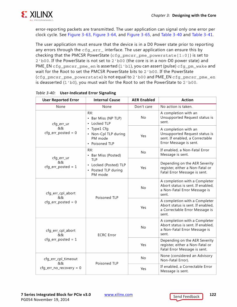
7 Series Integrated Block for PCIe v3.0 www.xilinx.com 122PG054 November 19, 2014
Chapter 3: Designing with the Core
error-reporting packets are transmitted. The user application can signal only one error per clock cycle. See Figure 3-63, Figure 3-64, and Figure 3-65, and Table 3-40 and Table 3-41.
The user application must ensure that the device is in a D0 Power state prior to reporting any errors through the cfg_err_ interface. The user application can ensure this by checking that the PMCSR PowerState (cfg_pmcsr_pme_powerstate[1:0]) is set to 2'b00. If the PowerState is not set to 2'b00 (the core is in a non-D0 power state) and PME_EN cfg_pmcsr_pme_en is asserted (1'b1), you can assert (pulse) cfg_pm_wake and wait for the Root to set the PMCSR PowerState bits to 2'b00. If the PowerState (cfg_pmcsr_pme_powerstate) is not equal to 2'b00 and PME_EN cfg_pmcsr_pme_en is deasserted (1'b0), you must wait for the Root to set the PowerState to 2'b00.
Table 3-40: User-Indicated Error Signaling
User Reported Error Internal Cause AER Enabled ActionNone None Don’t care No action is taken.
cfg_err_ur &&
cfg_err_posted = 0
RX: • Bar Miss (NP TLP) • Locked TLP• Type1 Cfg• Non-Cpl TLP during
PM mode • Poisoned TLP
NoA completion with an Unsupported Request status is sent.
Yes
A completion with an Unsupported Request status is sent. If enabled, a Correctable Error Message is sent.
cfg_err_ur&&
cfg_err_posted = 1
RX: • Bar Miss (Posted)
TLP• Locked (Posted) TLP• Posted TLP during
PM mode
No If enabled, a Non-Fatal Error Message is sent.
YesDepending on the AER Severity register, either a Non-Fatal or Fatal Error Message is sent.
cfg_err_cpl_abort&&
cfg_err_posted = 0Poisoned TLP
No
A completion with a Completer Abort status is sent. If enabled, a Non-Fatal Error Message is sent.
Yes
A completion with a Completer Abort status is sent. If enabled, a Correctable Error Message is sent.
cfg_err_cpl_abort&&
cfg_err_posted = 1ECRC Error
No
A completion with a Completer Abort status is sent. If enabled, a Non-Fatal Error Message is sent.
YesDepending on the AER Severity register, either a Non-Fatal or Fatal Error Message is sent.
cfg_err_cpl_timeout&&
cfg_err_no_recovery = 0Poisoned TLP
No None (considered an Advisory Non-Fatal Error).
Yes If enabled, a Correctable Error Message is sent.
Send Feedback
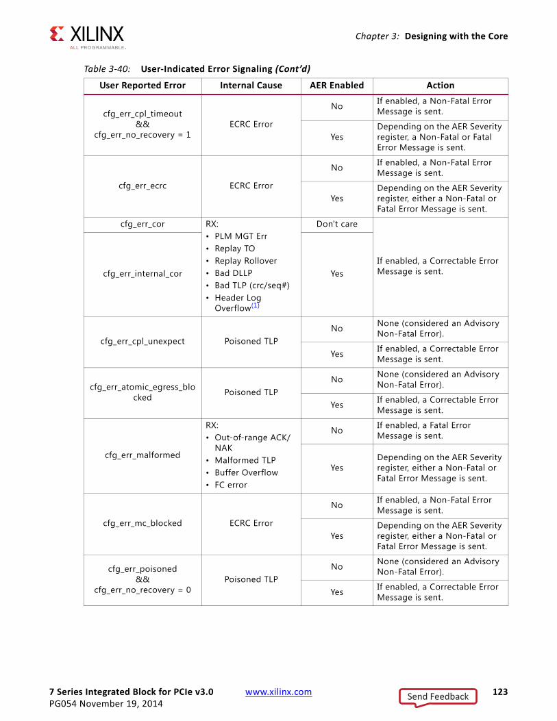
7 Series Integrated Block for PCIe v3.0 www.xilinx.com 123PG054 November 19, 2014
Chapter 3: Designing with the Core
cfg_err_cpl_timeout&&
cfg_err_no_recovery = 1ECRC Error
No If enabled, a Non-Fatal Error Message is sent.
YesDepending on the AER Severity register, a Non-Fatal or Fatal Error Message is sent.
cfg_err_ecrc ECRC Error
No If enabled, a Non-Fatal Error Message is sent.
YesDepending on the AER Severity register, either a Non-Fatal or Fatal Error Message is sent.
cfg_err_cor RX: • PLM MGT Err• Replay TO• Replay Rollover• Bad DLLP• Bad TLP (crc/seq#)• Header Log
Overflow(1)
Don't care
If enabled, a Correctable Error Message is sent.cfg_err_internal_cor Yes
cfg_err_cpl_unexpect Poisoned TLPNo None (considered an Advisory
Non-Fatal Error).
Yes If enabled, a Correctable Error Message is sent.
cfg_err_atomic_egress_blocked Poisoned TLP
No None (considered an Advisory Non-Fatal Error).
Yes If enabled, a Correctable Error Message is sent.
cfg_err_malformed
RX:• Out-of-range ACK/
NAK• Malformed TLP• Buffer Overflow• FC error
No If enabled, a Fatal Error Message is sent.
YesDepending on the AER Severity register, either a Non-Fatal or Fatal Error Message is sent.
cfg_err_mc_blocked ECRC Error
No If enabled, a Non-Fatal Error Message is sent.
YesDepending on the AER Severity register, either a Non-Fatal or Fatal Error Message is sent.
cfg_err_poisoned&&
cfg_err_no_recovery = 0Poisoned TLP
No None (considered an Advisory Non-Fatal Error).
Yes If enabled, a Correctable Error Message is sent.
Table 3-40: User-Indicated Error Signaling (Cont’d)
User Reported Error Internal Cause AER Enabled Action
Send Feedback

7 Series Integrated Block for PCIe v3.0 www.xilinx.com 124PG054 November 19, 2014
Chapter 3: Designing with the Core
Whenever an error is detected in a Non-Posted Request, the user application deasserts cfg_err_posted and provides header information on cfg_err_tlp_cpl_header[47:0] during the same clock cycle the error is reported, as illustrated in Figure 3-63. The additional header information is necessary to construct the required Completion with non-Successful status. Additional information about when to assert or deassert cfg_err_posted is provided in the remainder of this section.
If an error is detected on a Posted Request, the user application instead asserts cfg_err_posted, but otherwise follows the same signaling protocol. This results in a Non-Fatal Message to be sent, if enabled (see Figure 3-64).
If several non-Posted errors are signaled on cfg_err_ur or cfg_err_cpl_abort in a short amount of time, it is possible for the core to be unable to buffer them all. If that occurs, cfg_err_cpl_rdy is deasserted and you must cease signaling those types of errors on the same cycle. You must not resume signaling those types of errors until cfg_err_cpl_rdy is reasserted.
The ability of the core to generate error messages can be disabled by the Root Complex issuing a configuration write to the Endpoint core Device Control register and the PCI
cfg_err_poisoned&&
cfg_err_no_recovery = 1ECRC Error
No If enabled, a Non-Fatal Error Message is sent.
YesDepending on the AER Severity register, either a Non-Fatal or Fatal Error Message is sent.
Notes: 1. Only when AER is enabled.
Table 3-40: User-Indicated Error Signaling (Cont’d)
User Reported Error Internal Cause AER Enabled Action
Table 3-41: Possible Error Conditions for TLPs Received by the User Application
Rece
ived
TLP
Typ
e
Possible Error Condition Error Qualifying Signal Status
Unsupported Request
(cfg_err_ur)
Completion Abort
(cfg_err_cpl_abort)
Correctable Error
(cfg_err_cor)
ECRC Error (cfg_err_
ecrc)
Unexpected Completion
(cfg_err_cpl_unexpect)
Value to Drive on (cfg_err_
posted)
Drive Data on (cfg_err_tlp_
cpl header[47:0])
Memory Write 3 X N/A 3 X 1 No
Memory Read 3 3 N/A 3 X 0 Yes
I/O 3 3 N/A 3 X 0 Yes
Completion X X N/A 3 3 1 No
Notes: 1. A checkmark indicates a possible error condition for a given TLP type. For example, you can signal Unsupported Request or ECRC
Error for a Memory Write TLP, if these errors are detected. An X indicates not a valid error condition for a given TLP type. For example, you should never signal Completion Abort in response to a Memory Write TLP.
Send Feedback
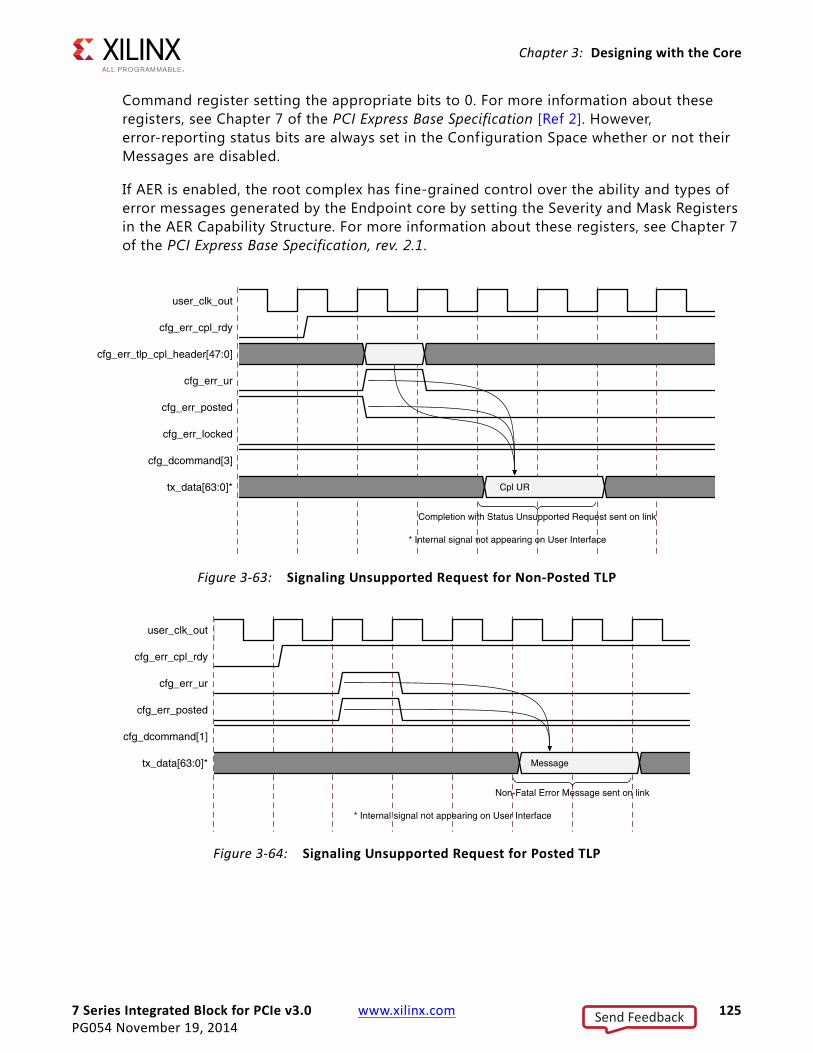
7 Series Integrated Block for PCIe v3.0 www.xilinx.com 125PG054 November 19, 2014
Chapter 3: Designing with the Core
Command register setting the appropriate bits to 0. For more information about these registers, see Chapter 7 of the PCI Express Base Specification [Ref 2]. However, error-reporting status bits are always set in the Configuration Space whether or not their Messages are disabled.
If AER is enabled, the root complex has f ine-grained control over the ability and types of error messages generated by the Endpoint core by setting the Severity and Mask Registers in the AER Capability Structure. For more information about these registers, see Chapter 7 of the PCI Express Base Specification, rev. 2.1.
X-Ref Target - Figure 3-63
Figure 3-63: Signaling Unsupported Request for Non-Posted TLP
user_clk_out
cfg_err_cpl_rdy
cfg_err_tlp_cpl_header[47:0]
cfg_err_ur
cfg_err_posted
cfg_err_locked
cfg_dcommand[3]
tx_data[63:0]* Cpl UR
Completion with Status Unsupported Request sent on link
* Internal signal not appearing on User Interface
X-Ref Target - Figure 3-64
Figure 3-64: Signaling Unsupported Request for Posted TLP
user_clk_out
cfg_err_cpl_rdy
cfg_err_ur
cfg_err_posted
cfg_dcommand[1]
tx_data[63:0]* Message
Non-Fatal Error Message sent on link
* Internal signal not appearing on User Interface
Send Feedback

7 Series Integrated Block for PCIe v3.0 www.xilinx.com 126PG054 November 19, 2014
Chapter 3: Designing with the Core
Completion Timeouts
The core does not implement Completion timers; for this reason, the user application must track how long its pending Non-Posted Requests have each been waiting for a Completion and trigger timeouts on them accordingly. The core has no method of knowing when such a timeout has occurred, and for this reason does not f ilter out inbound Completions for expired requests.
If a request times out, the user application must assert cfg_err_cpl_timeout, which causes an error message to be sent to the Root Complex. If a Completion is later received after a request times out, the user application must treat it as an Unexpected Completion.
Unexpected Completions
The core automatically reports Unexpected Completions in response to inbound Completions whose Requestor ID is different than the Endpoint ID programmed in the Configuration Space. These completions are not passed to the user application. The current version of the core regards an Unexpected Completion to be an Advisory Non-Fatal Error (ANFE), and no message is sent.
Completer Abort
If the user application is unable to transmit a normal Completion in response to a Non-Posted Request it receives, it must signal cfg_err_cpl_abort. The cfg_err_posted signal can also be set to 1 simultaneously to indicate Non-Posted and the appropriate request information placed on cfg_err_tlp_cpl_header[47:0]. This sends a Completion with non-Successful status to the original Requester, but does not send an Error Message. When in Legacy mode if the cfg_err_locked signal is set to 0 (to indicate the transaction causing the error was a locked transaction), a Completion Locked
X-Ref Target - Figure 3-65
Figure 3-65: Signaling Locked Unsupported Request for Locked Non-Posted TLP
user_clk_out
cfg_err_cpl_rdy
cfg_err_tlp_cpl_header[47:0]
cfg_err_ur
cfg_err_posted
cfg_err_locked
cfg_dcommand[3]
tx_data[63:0]* Cpl UR
Completion with Status Unsupported Request sent on link
* Internal signal not appearing on User Interface
Send Feedback

7 Series Integrated Block for PCIe v3.0 www.xilinx.com 127PG054 November 19, 2014
Chapter 3: Designing with the Core
with Non-Successful status is sent. If the cfg_err_posted signal is set to 1 (to indicate a Posted transaction), no Completion is sent, but a Non-Fatal Error Message is sent (if enabled).
Unsupported Request
If the user application receives an inbound Request it does not support or recognize, it must assert cfg_err_ur to signal an Unsupported Request. The cfg_err_posted signal must also be asserted or deasserted depending on whether the packet in question is a Posted or Non-Posted Request. If the packet is Posted, a Non-Fatal Error Message is sent out (if enabled); if the packet is Non-Posted, a Completion with a non-Successful status is sent to the original Requester. When in Legacy mode if the cfg_err_locked signal is set to 1 (to indicate the transaction causing the error was a locked transaction), a Completion Locked with Unsupported Request status is sent.
The Unsupported Request condition can occur for several reasons, including:
• An inbound Memory Write packet violates the programming model of the user application, for example, if the user application is allotted a 4 KB address space but only uses 3 KB, and the inbound packet addresses the unused portion.
Note: If this occurs on a Non-Posted Request, the user application should use cfg_err_cpl_abort to flag the error.
• An inbound packet uses a packet Type not supported by the user application, for example, an I/O request to a memory-only device.
ECRC Error
When enabled, the core automatically checks the ECRC field for validity. If an ECRC error is detected, the core responds by setting the appropriate status bits and an appropriate error message is sent, if enabled to do so in the configuration space.
If automatic ECRC checking is disabled, the user application can still signal an ECRC error by asserting cfg_err_ecrc. The user application should only assert cfg_err_ecrc if AER is disabled.
AER Requirements
Whenever the user application signals an error using one of the cfg_err_* inputs (for example, cfg_err_ecrc_n), it must also log the header of the TLP that caused the error. The user application provides header information on cfg_err_aer_headerlog[127:0] during the same clock cycle the error is reported. The user application must hold the header information until cfg_err_aer_headerlog_set is asserted. cfg_err_aer_headerlog_set remains asserted until the Uncorrectable Error Status Register bit corresponding to the first error pointer is cleared (typically, through system software – see the PCI Express Base Specification, v2.1 [Ref 2]). If cfg_err_aer_headerlog_set is already asserted, there is already a header logged. Figure 3-66 illustrates the operation for AER header logging.
Send Feedback
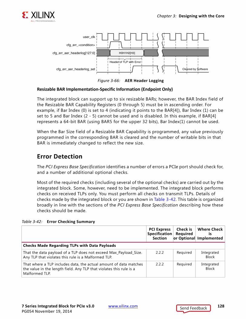
7 Series Integrated Block for PCIe v3.0 www.xilinx.com 128PG054 November 19, 2014
Chapter 3: Designing with the Core
Resizable BAR Implementation-Specific Information (Endpoint Only)
The integrated block can support up to six resizable BARs; however, the BAR Index f ield of the Resizable BAR Capability Registers (0 through 5) must be in ascending order. For example, if Bar Index (0) is set to 4 (indicating it points to the BAR[4]), Bar Index (1) can be set to 5 and Bar Index (2 - 5) cannot be used and is disabled. In this example, if BAR[4] represents a 64-bit BAR (using BAR5 for the upper 32 bits), Bar Index(1) cannot be used.
When the Bar Size f ield of a Resizable BAR Capability is programmed, any value previously programmed in the corresponding BAR is cleared and the number of writable bits in that BAR is immediately changed to reflect the new size.
Error DetectionThe PCI Express Base Specification identif ies a number of errors a PCIe port should check for, and a number of additional optional checks.
Most of the required checks (including several of the optional checks) are carried out by the integrated block. Some, however, need to be implemented. The integrated block performs checks on received TLPs only. You must perform all checks on transmit TLPs. Details of checks made by the integrated block or you are shown in Table 3-42. This table is organized broadly in line with the sections of the PCI Express Base Specification describing how these checks should be made.
X-Ref Target - Figure 3-66
Figure 3-66: AER Header Logging
user_clk
cfg_err_<condition>
cfg_err_aer_headerlog[127:0]
cfg_err_aer_headerlog_set
H0H1H2[H3]
Cleared by Software
Header of TLP with Error
Table 3-42: Error Checking Summary
PCI Express Specification
Section
Check is Required
or Optional
Where Check is
Implemented
Checks Made Regarding TLPs with Data Payloads
That the data payload of a TLP does not exceed Max_Payload_Size. Any TLP that violates this rule is a Malformed TLP.
2.2.2 Required Integrated Block
That where a TLP includes data, the actual amount of data matches the value in the length f ield. Any TLP that violates this rule is a Malformed TLP.
2.2.2 Required Integrated Block
Send Feedback
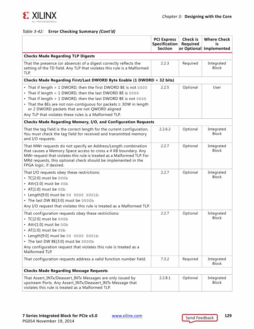
7 Series Integrated Block for PCIe v3.0 www.xilinx.com 129PG054 November 19, 2014
Chapter 3: Designing with the Core
Checks Made Regarding TLP Digests
That the presence (or absence) of a digest correctly reflects the setting of the TD f ield. Any TLP that violates this rule is a Malformed TLP.
2.2.3 Required Integrated Block
Checks Made Regarding First/Last DWORD Byte Enable (1 DWORD = 32 bits)
• That if length > 1 DWORD, then the first DWORD BE is not 0000• That if length = 1 DWORD, then the last DWORD BE is 0000• That if length > 1 DWORD, then the last DWORD BE is not 0000• That the BEs are not non-contiguous for packets ≥ 3DW in length
or 2 DWORD packets that are not QWORD alignedAny TLP that violates these rules is a Malformed TLP.
2.2.5 Optional User
Checks Made Regarding Memory, I/O, and Configuration Requests
That the tag f ield is the correct length for the current configuration. You must check the tag field for received and transmitted memory and I/O requests.
2.2.6.2 Optional Integrated Block
That MWr requests do not specify an Address/Length combination that causes a Memory Space access to cross a 4 KB boundary. Any MWr request that violates this rule is treated as a Malformed TLP. For MRd requests, this optional check should be implemented in the FPGA logic, if desired.
2.2.7 Optional Integrated Block
That I/O requests obey these restrictions:• TC[2:0] must be 000b• Attr[1:0] must be 00b• AT[1:0] must be 00b • Length[9:0] must be 00 0000 0001b• The last DW BE[3:0] must be 0000bAny I/O request that violates this rule is treated as a Malformed TLP.
2.2.7 Optional Integrated Block
That configuration requests obey these restrictions:• TC[2:0] must be 000b• Attr[1:0] must be 00b• AT[1:0] must be 00b • Length[9:0] must be 00 0000 0001b• The last DW BE[3:0] must be 0000bAny configuration request that violates this rule is treated as a Malformed TLP.
2.2.7 Optional Integrated Block
That configuration requests address a valid function number f ield. 7.3.2 Required Integrated Block
Checks Made Regarding Message Requests
That Assert_INTx/Deassert_INTx Messages are only issued by upstream Ports. Any Assert_INTx/Deassert_INTx Message that violates this rule is treated as a Malformed TLP.
2.2.8.1 Optional Integrated Block
Table 3-42: Error Checking Summary (Cont’d)
PCI Express Specification
Section
Check is Required
or Optional
Where Check is
Implemented
Send Feedback
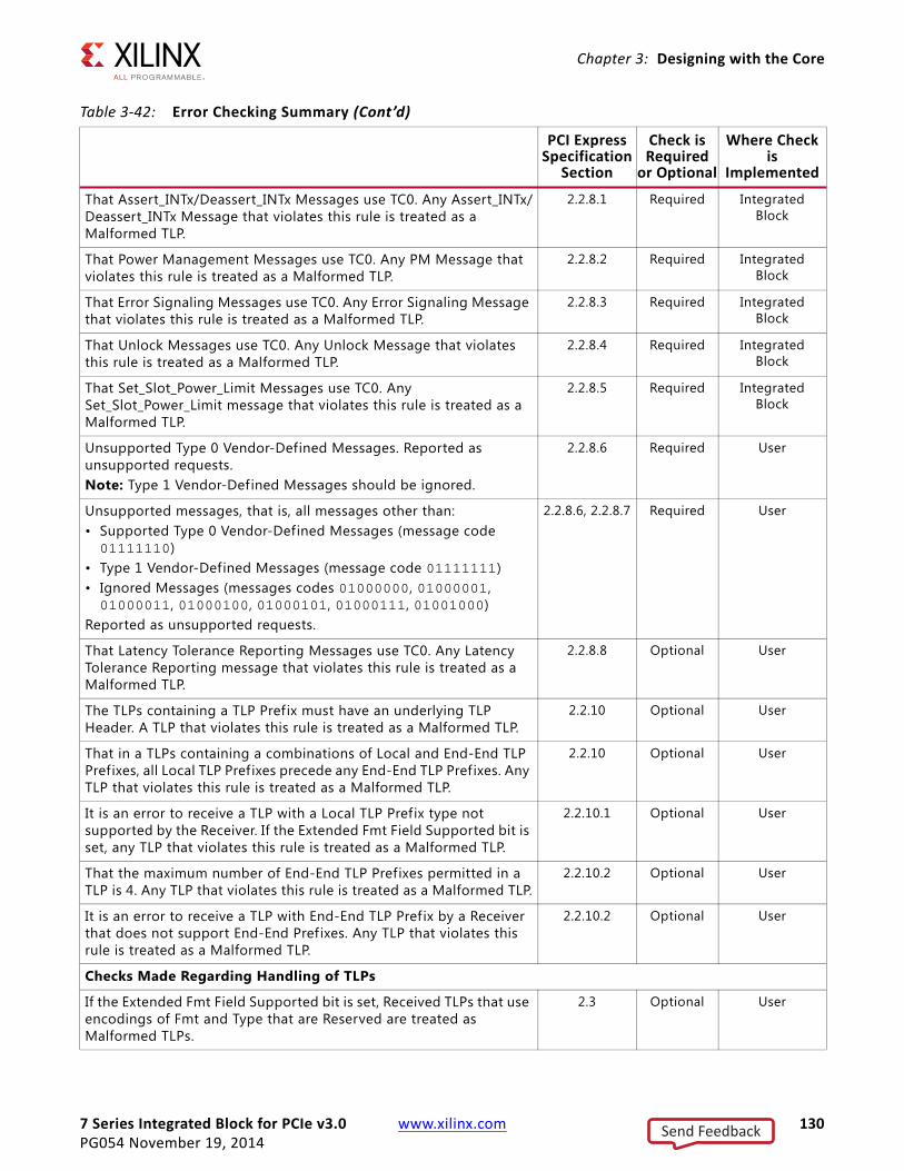
7 Series Integrated Block for PCIe v3.0 www.xilinx.com 130PG054 November 19, 2014
Chapter 3: Designing with the Core
That Assert_INTx/Deassert_INTx Messages use TC0. Any Assert_INTx/Deassert_INTx Message that violates this rule is treated as a Malformed TLP.
2.2.8.1 Required Integrated Block
That Power Management Messages use TC0. Any PM Message that violates this rule is treated as a Malformed TLP.
2.2.8.2 Required Integrated Block
That Error Signaling Messages use TC0. Any Error Signaling Message that violates this rule is treated as a Malformed TLP.
2.2.8.3 Required Integrated Block
That Unlock Messages use TC0. Any Unlock Message that violates this rule is treated as a Malformed TLP.
2.2.8.4 Required Integrated Block
That Set_Slot_Power_Limit Messages use TC0. Any Set_Slot_Power_Limit message that violates this rule is treated as a Malformed TLP.
2.2.8.5 Required Integrated Block
Unsupported Type 0 Vendor-Defined Messages. Reported as unsupported requests. Note: Type 1 Vendor-Defined Messages should be ignored.
2.2.8.6 Required User
Unsupported messages, that is, all messages other than:• Supported Type 0 Vendor-Defined Messages (message code 01111110)
• Type 1 Vendor-Defined Messages (message code 01111111)• Ignored Messages (messages codes 01000000, 01000001, 01000011, 01000100, 01000101, 01000111, 01001000)
Reported as unsupported requests.
2.2.8.6, 2.2.8.7 Required User
That Latency Tolerance Reporting Messages use TC0. Any Latency Tolerance Reporting message that violates this rule is treated as a Malformed TLP.
2.2.8.8 Optional User
The TLPs containing a TLP Prefix must have an underlying TLP Header. A TLP that violates this rule is treated as a Malformed TLP.
2.2.10 Optional User
That in a TLPs containing a combinations of Local and End-End TLP Prefixes, all Local TLP Prefixes precede any End-End TLP Prefixes. Any TLP that violates this rule is treated as a Malformed TLP.
2.2.10 Optional User
It is an error to receive a TLP with a Local TLP Prefix type not supported by the Receiver. If the Extended Fmt Field Supported bit is set, any TLP that violates this rule is treated as a Malformed TLP.
2.2.10.1 Optional User
That the maximum number of End-End TLP Prefixes permitted in a TLP is 4. Any TLP that violates this rule is treated as a Malformed TLP.
2.2.10.2 Optional User
It is an error to receive a TLP with End-End TLP Prefix by a Receiver that does not support End-End Prefixes. Any TLP that violates this rule is treated as a Malformed TLP.
2.2.10.2 Optional User
Checks Made Regarding Handling of TLPs
If the Extended Fmt Field Supported bit is set, Received TLPs that use encodings of Fmt and Type that are Reserved are treated as Malformed TLPs.
2.3 Optional User
Table 3-42: Error Checking Summary (Cont’d)
PCI Express Specification
Section
Check is Required
or Optional
Where Check is
Implemented
Send Feedback
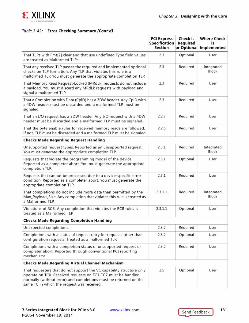
7 Series Integrated Block for PCIe v3.0 www.xilinx.com 131PG054 November 19, 2014
Chapter 3: Designing with the Core
That TLPs with Fmt[2] clear and that use undefined Type field values are treated as Malformed TLPs.
2.3 Optional User
That any received TLP passes the required and implemented optional checks on TLP formation. Any TLP that violates this rule is a malformed TLP. You must generate the appropriate completion TLP.
2.3 Required Integrated Block
That Memory Read Request-Locked (MRdLk) requests do not include a payload. You must discard any MRdLk requests with payload and signal a malformed TLP.
2.3 Required User
That a Completion with Data (CplD) has a 3DW header. Any CplD with a 4DW header must be discarded and a malformed TLP must be signaled.
2.3 Required User
That an I/O request has a 3DW header. Any I/O request with a 4DW header must be discarded and a malformed TLP must be signaled.
2.2.7 Required User
That the byte enable rules for received memory reads are followed. If not, TLP must be discarded and a malformed TLP must be signaled.
2.2.5 Required User
Checks Made Regarding Request Handling
Unsupported request types. Reported as an unsupported request. You must generate the appropriate completion TLP.
2.3.1 Required Integrated Block
Requests that violate the programming model of the device. Reported as a completer abort. You must generate the appropriate completion TLP.
2.3.1 Optional User
Requests that cannot be processed due to a device-specif ic error condition. Reported as a completer abort. You must generate the appropriate completion TLP.
2.3.1 Required User
That completions do not include more data than permitted by the Max_Payload_Size. Any completion that violates this rule is treated as a Malformed TLP.
2.3.1.1 Required Integrated Block
Violations of RCB. Any completion that violates the RCB rules is treated as a Malformed TLP.
2.3.1.1 Optional User
Checks Made Regarding Completion Handling
Unexpected completions. 2.3.2 Required User
Completions with a status of request retry for requests other than configuration requests. Treated as a malformed TLP.
2.3.2 Optional User
Completions with a completion status of unsupported request or completer abort. Reported through conventional PCI reporting mechanisms.
2.3.2 Required User
Checks Made Regarding Virtual Channel Mechanism
That requesters that do not support the VC capability structure only operate on TC0. Received requests on TC1-TC7 must be handled normally (without error) and completions must be returned on the same TC in which the request was received.
2.5 Optional User
Table 3-42: Error Checking Summary (Cont’d)
PCI Express Specification
Section
Check is Required
or Optional
Where Check is
Implemented
Send Feedback
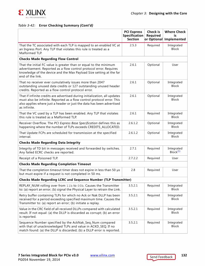
7 Series Integrated Block for PCIe v3.0 www.xilinx.com 132PG054 November 19, 2014
Chapter 3: Designing with the Core
That the TC associated with each TLP is mapped to an enabled VC at an Ingress Port. Any TLP that violates this rule is treated as a Malformed TLP.
2.5.3 Required Integrated Block
Checks Made Regarding Flow Control
That the initial FC value is greater than or equal to the minimum advertisement. Reported as a flow control protocol error. Requires knowledge of the device and the Max Payload Size setting at the far end of the link.
2.6.1 Optional User
That no receiver ever cumulatively issues more than 2047 outstanding unused data credits or 127 outstanding unused header credits. Reported as a flow control protocol error.
2.6.1 Optional Integrated Block
That if infinite credits are advertised during initialization, all updates must also be infinite. Reported as a flow control protocol error. This also applies where just a header or just the data has been advertised as infinite.
2.6.1 Optional Integrated Block
That the VC used by a TLP has been enabled. Any TLP that violates this rule is treated as a Malformed TLP.
2.6.1 Required Integrated Block
Receiver Overflow. The PCI Express Base Specification defines this as happening where the number of TLPs exceeds CREDITS_ALLOCATED.
2.6.1.2 Optional Integrated Block
That Update FCPs are scheduled for transmission at the specif ied interval.
2.6.1.2 Optional Integrated Block
Checks Made Regarding Data Integrity
Integrity of TD bit in messages received and forwarded by switches. Any failed ECRC checks are reported.
2.7.1 Required Integrated Block(1)
Receipt of a Poisoned TLP. 2.7.2.2 Required User
Checks Made Regarding Completion Timeout
That the completion timeout timer does not expire in less than 50 µs but must expire if a request is not completed in 50 ms.
2.8 Required User
Checks Made Regarding LCRC and Sequence Number (TLP Transmitter)
REPLAY_NUM rolling over from 11b to 00b. Causes the Transmitter to: (a) report an error; (b) signal the Physical Layer to retrain the Link.
3.5.2.1 Required Integrated Block
Retry buffer containing TLPs for which no Ack or Nak DLLP has been received for a period exceeding specif ied maximum time. Causes the Transmitter to: (a) report an error; (b) initiate a replay.
3.5.2.1 Required Integrated Block
Value in the CRC f ield of all received DLLPs compared with calculated result. If not equal: (a) the DLLP is discarded as corrupt; (b) an error is reported.
3.5.2.1 Required Integrated Block
Sequence Number specif ied by the AckNak_Seq_Num compared with that of unacknowledged TLPs and value in ACKD_SEQ. If no match found: (a) the DLLP is discarded; (b) a DLLP error is reported.
3.5.2.1 Required Integrated Block
Table 3-42: Error Checking Summary (Cont’d)
PCI Express Specification
Section
Check is Required
or Optional
Where Check is
Implemented
Send Feedback
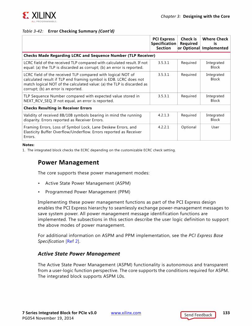
7 Series Integrated Block for PCIe v3.0 www.xilinx.com 133PG054 November 19, 2014
Chapter 3: Designing with the Core
Power ManagementThe core supports these power management modes:
• Active State Power Management (ASPM)
• Programmed Power Management (PPM)
Implementing these power management functions as part of the PCI Express design enables the PCI Express hierarchy to seamlessly exchange power-management messages to save system power. All power management message identif ication functions are implemented. The subsections in this section describe the user logic definition to support the above modes of power management.
For additional information on ASPM and PPM implementation, see the PCI Express Base Specification [Ref 2].
Active State Power Management
The Active State Power Management (ASPM) functionality is autonomous and transparent from a user-logic function perspective. The core supports the conditions required for ASPM. The integrated block supports ASPM L0s.
Checks Made Regarding LCRC and Sequence Number (TLP Receiver)
LCRC field of the received TLP compared with calculated result. If not equal: (a) the TLP is discarded as corrupt; (b) an error is reported.
3.5.3.1 Required Integrated Block
LCRC field of the received TLP compared with logical NOT of calculated result if TLP end framing symbol is EDB. LCRC does not match logical NOT of the calculated value: (a) the TLP is discarded as corrupt; (b) an error is reported.
3.5.3.1 Required Integrated Block
TLP Sequence Number compared with expected value stored in NEXT_RCV_SEQ. If not equal, an error is reported.
3.5.3.1 Required Integrated Block
Checks Resulting in Receiver Errors
Validity of received 8B/10B symbols bearing in mind the running disparity. Errors reported as Receiver Errors.
4.2.1.3 Required Integrated Block
Framing Errors, Loss of Symbol Lock, Lane Deskew Errors, and Elasticity Buffer Overflow/Underflow. Errors reported as Receiver Errors.
4.2.2.1 Optional User
Notes: 1. The integrated block checks the ECRC depending on the customizable ECRC check setting.
Table 3-42: Error Checking Summary (Cont’d)
PCI Express Specification
Section
Check is Required
or Optional
Where Check is
Implemented
Send Feedback
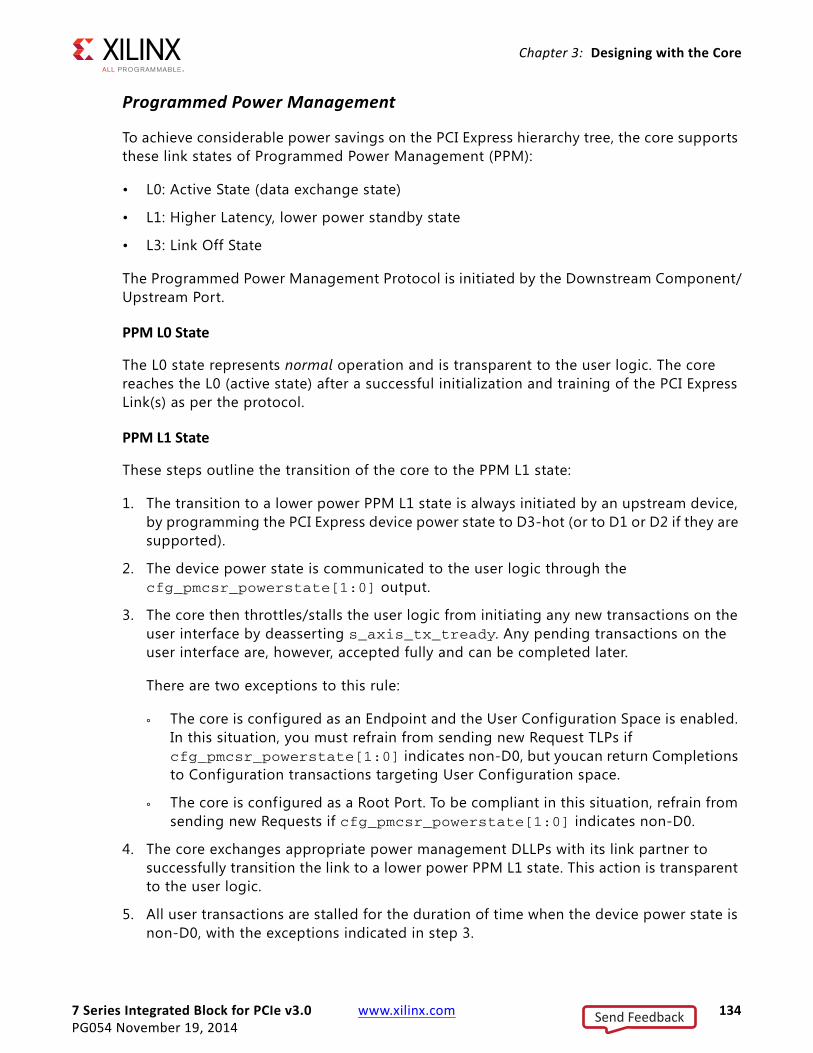
7 Series Integrated Block for PCIe v3.0 www.xilinx.com 134PG054 November 19, 2014
Chapter 3: Designing with the Core
Programmed Power Management
To achieve considerable power savings on the PCI Express hierarchy tree, the core supports these link states of Programmed Power Management (PPM):
• L0: Active State (data exchange state)
• L1: Higher Latency, lower power standby state
• L3: Link Off State
The Programmed Power Management Protocol is initiated by the Downstream Component/Upstream Port.
PPM L0 State
The L0 state represents normal operation and is transparent to the user logic. The core reaches the L0 (active state) after a successful initialization and training of the PCI Express Link(s) as per the protocol.
PPM L1 State
These steps outline the transition of the core to the PPM L1 state:
1. The transition to a lower power PPM L1 state is always initiated by an upstream device, by programming the PCI Express device power state to D3-hot (or to D1 or D2 if they are supported).
2. The device power state is communicated to the user logic through the cfg_pmcsr_powerstate[1:0] output.
3. The core then throttles/stalls the user logic from initiating any new transactions on the user interface by deasserting s_axis_tx_tready. Any pending transactions on the user interface are, however, accepted fully and can be completed later.
There are two exceptions to this rule:
° The core is configured as an Endpoint and the User Configuration Space is enabled. In this situation, you must refrain from sending new Request TLPs if cfg_pmcsr_powerstate[1:0] indicates non-D0, but youcan return Completions to Configuration transactions targeting User Configuration space.
° The core is configured as a Root Port. To be compliant in this situation, refrain from sending new Requests if cfg_pmcsr_powerstate[1:0] indicates non-D0.
4. The core exchanges appropriate power management DLLPs with its link partner to successfully transition the link to a lower power PPM L1 state. This action is transparent to the user logic.
5. All user transactions are stalled for the duration of time when the device power state is non-D0, with the exceptions indicated in step 3.
Send Feedback
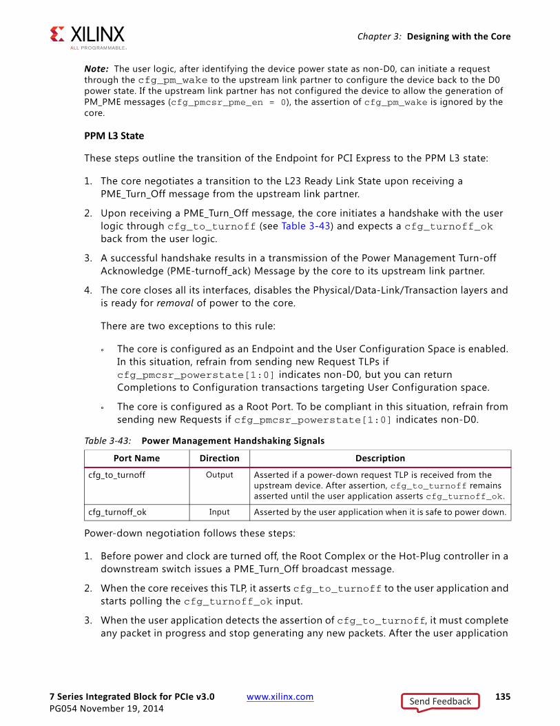
7 Series Integrated Block for PCIe v3.0 www.xilinx.com 135PG054 November 19, 2014
Chapter 3: Designing with the Core
Note: The user logic, after identifying the device power state as non-D0, can initiate a request through the cfg_pm_wake to the upstream link partner to configure the device back to the D0 power state. If the upstream link partner has not configured the device to allow the generation of PM_PME messages (cfg_pmcsr_pme_en = 0), the assertion of cfg_pm_wake is ignored by the core.
PPM L3 State
These steps outline the transition of the Endpoint for PCI Express to the PPM L3 state:
1. The core negotiates a transition to the L23 Ready Link State upon receiving a PME_Turn_Off message from the upstream link partner.
2. Upon receiving a PME_Turn_Off message, the core initiates a handshake with the user logic through cfg_to_turnoff (see Table 3-43) and expects a cfg_turnoff_ok back from the user logic.
3. A successful handshake results in a transmission of the Power Management Turn-off Acknowledge (PME-turnoff_ack) Message by the core to its upstream link partner.
4. The core closes all its interfaces, disables the Physical/Data-Link/Transaction layers and is ready for removal of power to the core.
There are two exceptions to this rule:
° The core is configured as an Endpoint and the User Configuration Space is enabled. In this situation, refrain from sending new Request TLPs if cfg_pmcsr_powerstate[1:0] indicates non-D0, but you can return Completions to Configuration transactions targeting User Configuration space.
° The core is configured as a Root Port. To be compliant in this situation, refrain from sending new Requests if cfg_pmcsr_powerstate[1:0] indicates non-D0.
Power-down negotiation follows these steps:
1. Before power and clock are turned off, the Root Complex or the Hot-Plug controller in a downstream switch issues a PME_Turn_Off broadcast message.
2. When the core receives this TLP, it asserts cfg_to_turnoff to the user application and starts polling the cfg_turnoff_ok input.
3. When the user application detects the assertion of cfg_to_turnoff, it must complete any packet in progress and stop generating any new packets. After the user application
Table 3-43: Power Management Handshaking Signals
Port Name Direction Description
cfg_to_turnoff Output Asserted if a power-down request TLP is received from the upstream device. After assertion, cfg_to_turnoff remains asserted until the user application asserts cfg_turnoff_ok .
cfg_turnoff_ok Input Asserted by the user application when it is safe to power down.
Send Feedback

7 Series Integrated Block for PCIe v3.0 www.xilinx.com 136PG054 November 19, 2014
Chapter 3: Designing with the Core
is ready to be turned off, it asserts cfg_turnoff_ok to the core. After assertion of cfg_turnoff_ok , the user application has committed to being turned off.
4. The core sends a PME_TO_Ack when it detects assertion of cfg_turnoff_ok , as displayed in Figure 3-67 (64-bit).
Generating Interrupt RequestsNote: This section is only applicable to the Endpoint Configuration of the 7 Series FPGAs Integrated Block for PCI Express core.
The core supports sending interrupt requests as either legacy, Message MSI, or MSI-X interrupts. The mode is programmed using the MSI Enable bit in the Message Control Register of the MSI Capability Structure and the MSI-X Enable bit in the MSI-X Message Control Register of the MSI-X Capability Structure. For more information on the MSI and MSI-X capability structures, see section 6.8 of the PCI Local Base Specification v3.0 [Ref 2].
The state of the MSI Enable and MSI-X Enabled bits are reflected by the cfg_interrupt_msienable and cfg_interrupt_msixeable outputs, respectively. Table 3-44 describes the Interrupt Mode the device has been programmed to, based on the cfg_interrupt_msienable and cfg_interrupt_msixenable outputs of the core.
X-Ref Target - Figure 3-67
Figure 3-67: Power Management Handshaking: 64-Bit
user_clk_out
rx_data[63:0]*
cfg_to_turnoff
cfg_turnoff_ok
tx_data[63:0]*
PME_Turn_Off
PME_TO_ACK
* Internal signal not appearing on User Interface
Table 3-44: Interrupt Modes
cfg_interrupt_msixenable=0 cfg_interrupt_msixenable=1
cfg_interrupt_msienable=0
Legacy Interrupt (INTx) mode.The cfg_interrupt interface only sends INTx messages.
MSI-X mode. You must generate MSI-X interrupts by composing MWr TLPs on the transmit AXI4-Stream interface; Do not use the cfg_interrupt interface.The cfg_interrupt interface is active and sends INTx messages, but refrain from doing so.
cfg_interrupt_msienable=1
MSI mode. The cfg_interrupt interface only sends MSI interrupts (MWr TLPs).
Undefined. System software is not supposed to permit this. However, the cfg_interrupt interface is active and sends MSI interrupts (MWr TLPs) if you choose to do so.
Send Feedback
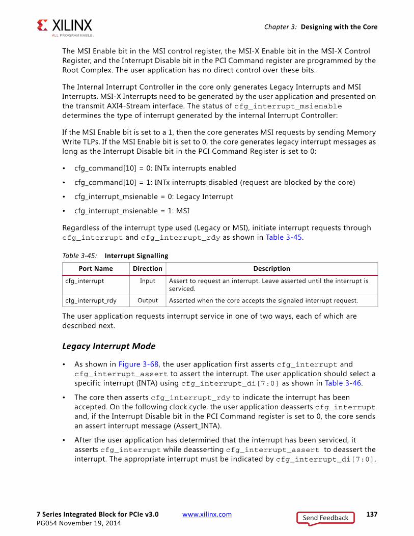
7 Series Integrated Block for PCIe v3.0 www.xilinx.com 137PG054 November 19, 2014
Chapter 3: Designing with the Core
The MSI Enable bit in the MSI control register, the MSI-X Enable bit in the MSI-X Control Register, and the Interrupt Disable bit in the PCI Command register are programmed by the Root Complex. The user application has no direct control over these bits.
The Internal Interrupt Controller in the core only generates Legacy Interrupts and MSI Interrupts. MSI-X Interrupts need to be generated by the user application and presented on the transmit AXI4-Stream interface. The status of cfg_interrupt_msienable determines the type of interrupt generated by the internal Interrupt Controller:
If the MSI Enable bit is set to a 1, then the core generates MSI requests by sending Memory Write TLPs. If the MSI Enable bit is set to 0, the core generates legacy interrupt messages as long as the Interrupt Disable bit in the PCI Command Register is set to 0:
• cfg_command[10] = 0: INTx interrupts enabled
• cfg_command[10] = 1: INTx interrupts disabled (request are blocked by the core)
• cfg_interrupt_msienable = 0: Legacy Interrupt
• cfg_interrupt_msienable = 1: MSI
Regardless of the interrupt type used (Legacy or MSI), initiate interrupt requests through cfg_interrupt and cfg_interrupt_rdy as shown in Table 3-45.
The user application requests interrupt service in one of two ways, each of which are described next.
Legacy Interrupt Mode
• As shown in Figure 3-68, the user application f irst asserts cfg_interrupt and cfg_interrupt_assert to assert the interrupt. The user application should select a specific interrupt (INTA) using cfg_interrupt_di[7:0] as shown in Table 3-46.
• The core then asserts cfg_interrupt_rdy to indicate the interrupt has been accepted. On the following clock cycle, the user application deasserts cfg_interrupt and, if the Interrupt Disable bit in the PCI Command register is set to 0, the core sends an assert interrupt message (Assert_INTA).
• After the user application has determined that the interrupt has been serviced, it asserts cfg_interrupt while deasserting cfg_interrupt_assert to deassert the interrupt. The appropriate interrupt must be indicated by cfg_interrupt_di[7:0].
Table 3-45: Interrupt Signalling
Port Name Direction Description
cfg_interrupt Input Assert to request an interrupt. Leave asserted until the interrupt is serviced.
cfg_interrupt_rdy Output Asserted when the core accepts the signaled interrupt request.
Send Feedback
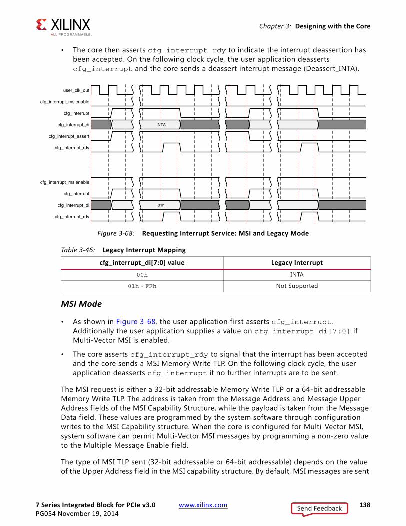
7 Series Integrated Block for PCIe v3.0 www.xilinx.com 138PG054 November 19, 2014
Chapter 3: Designing with the Core
• The core then asserts cfg_interrupt_rdy to indicate the interrupt deassertion has been accepted. On the following clock cycle, the user application deasserts cfg_interrupt and the core sends a deassert interrupt message (Deassert_INTA).
MSI Mode
• As shown in Figure 3-68, the user application f irst asserts cfg_interrupt. Additionally the user application supplies a value on cfg_interrupt_di[7:0] if Multi-Vector MSI is enabled.
• The core asserts cfg_interrupt_rdy to signal that the interrupt has been accepted and the core sends a MSI Memory Write TLP. On the following clock cycle, the user application deasserts cfg_interrupt if no further interrupts are to be sent.
The MSI request is either a 32-bit addressable Memory Write TLP or a 64-bit addressable Memory Write TLP. The address is taken from the Message Address and Message Upper Address f ields of the MSI Capability Structure, while the payload is taken from the Message Data f ield. These values are programmed by the system software through configuration writes to the MSI Capability structure. When the core is configured for Multi-Vector MSI, system software can permit Multi-Vector MSI messages by programming a non-zero value to the Multiple Message Enable f ield.
The type of MSI TLP sent (32-bit addressable or 64-bit addressable) depends on the value of the Upper Address field in the MSI capability structure. By default, MSI messages are sent
X-Ref Target - Figure 3-68
Figure 3-68: Requesting Interrupt Service: MSI and Legacy Mode
user_clk_out
cfg_interrupt_msienable
cfg_interrupt
cfg_interrupt_di
cfg_interrupt_assert
cfg_interrupt_rdy
cfg_interrupt_msienable
cfg_interrupt
cfg_interrupt_di
cfg_interrupt_rdy
INTA
01h
Table 3-46: Legacy Interrupt Mapping
cfg_interrupt_di[7:0] value Legacy Interrupt
00h INTA
01h - FFh Not Supported
Send Feedback
7 Series Integrated Block for PCIe v3.0 www.xilinx.com 139PG054 November 19, 2014
Chapter 3: Designing with the Core
as 32-bit addressable Memory Write TLPs. MSI messages use 64-bit addressable Memory Write TLPs only if the system software programs a non-zero value into the Upper Address register.
When Multi-Vector MSI messages are enabled, the user application can override one or more of the lower-order bits in the Message Data f ield of each transmitted MSI TLP to differentiate between the various MSI messages sent upstream. The number of lower-order bits in the Message Data field available to the user application is determined by the lesser of the value of the Multiple Message Capable field, as set in the Vivado IDE, and the Multiple Message Enable field, as set by system software and available as the cfg_interrupt_mmenable[2:0] core output. The core masks any bits in cfg_interrupt_di[7:0] which are not configured by the system software through Multiple Message Enable.
This pseudo code shows the processing required:
// Value MSI_Vector_Num must be in range: 0 ≤ MSI_Vector_Num ≤ (2^cfg_interrupt_mmenable)-1
if (cfg_interrupt_msienable) { // MSI Enabledif (cfg_interrupt_mmenable > 0) { // Multi-Vector MSI Enabled
cfg_interrupt_di[7:0] = {Padding_0s, MSI_Vector_Num};} else { // Single-Vector MSI Enabled
cfg_interrupt_di[7:0] = Padding_0s;}
} else {// Legacy Interrupts Enabled
}
For example:
1. If cfg_interrupt_mmenable[2:0] == 000b, that is, 1 MSI Vector Enabled, then cfg_interrupt_di[7:0] = 00h;
2. if cfg_interrupt_mmenable[2:0] == 101b, that is, 32 MSI Vectors Enabled, then cfg_interrupt_di[7:0] = {{000b}, {MSI_Vector#}};
where MSI_Vector# is a 5-bit value and is allowed to be 00000b ≤ MSI_Vector# ≤ 11111b.
If Per-Vector Masking is enabled, you must f irst verify that the vector being signaled is not masked in the Mask register. This is done by reading this register on the Configuration interface (the core does not look at the Mask register).
MSI-X Mode
The core optionally supports the MSI-X Capability Structure. The MSI-X vector table and the MSI-X Pending Bit Array need to be implemented as part of your logic, by claiming a BAR aperture.
If the cfg_interrupt_msixenable output of the core is asserted, the user application should compose and present the MSI-X interrupts on the transmit AXI4-Stream interface.
Send Feedback
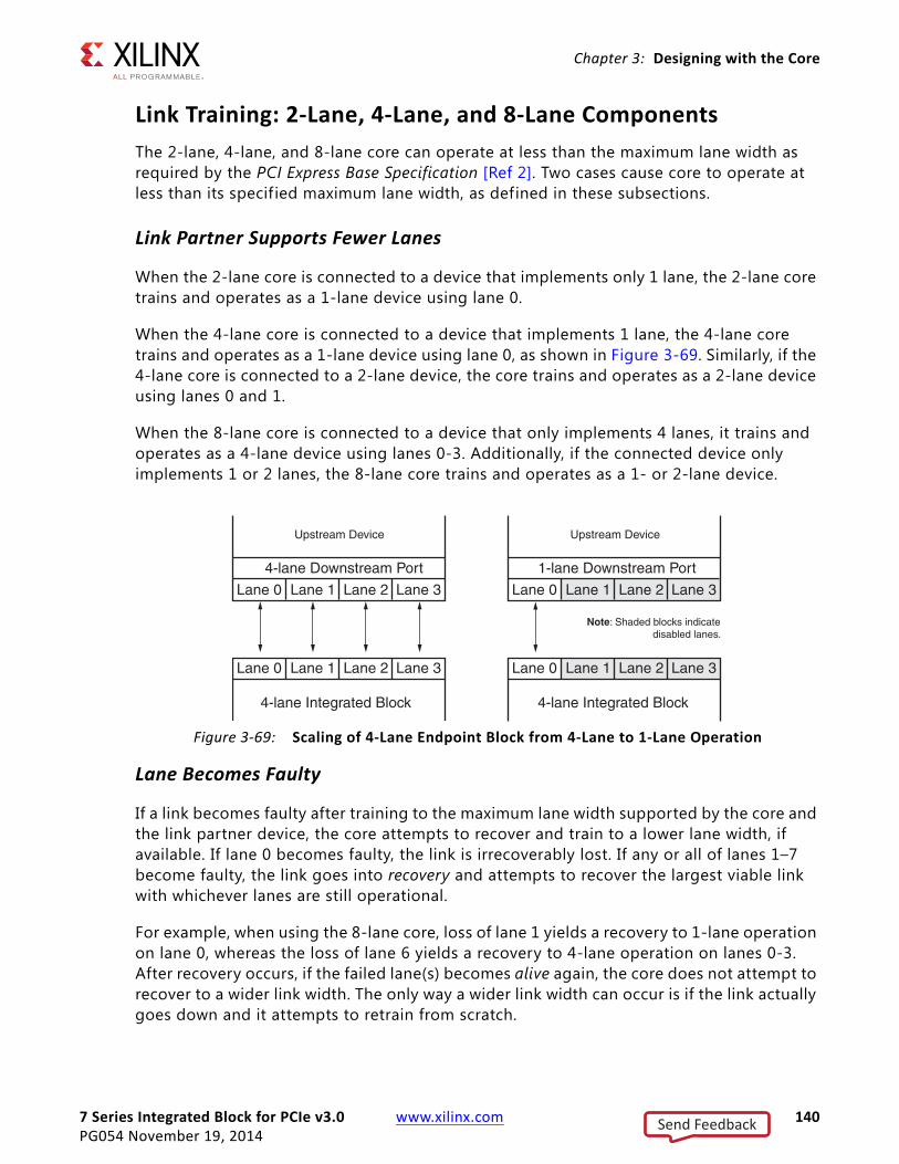
7 Series Integrated Block for PCIe v3.0 www.xilinx.com 140PG054 November 19, 2014
Chapter 3: Designing with the Core
Link Training: 2-Lane, 4-Lane, and 8-Lane ComponentsThe 2-lane, 4-lane, and 8-lane core can operate at less than the maximum lane width as required by the PCI Express Base Specification [Ref 2]. Two cases cause core to operate at less than its specif ied maximum lane width, as defined in these subsections.
Link Partner Supports Fewer Lanes
When the 2-lane core is connected to a device that implements only 1 lane, the 2-lane core trains and operates as a 1-lane device using lane 0.
When the 4-lane core is connected to a device that implements 1 lane, the 4-lane core trains and operates as a 1-lane device using lane 0, as shown in Figure 3-69. Similarly, if the 4-lane core is connected to a 2-lane device, the core trains and operates as a 2-lane device using lanes 0 and 1.
When the 8-lane core is connected to a device that only implements 4 lanes, it trains and operates as a 4-lane device using lanes 0-3. Additionally, if the connected device only implements 1 or 2 lanes, the 8-lane core trains and operates as a 1- or 2-lane device.
Lane Becomes Faulty
If a link becomes faulty after training to the maximum lane width supported by the core and the link partner device, the core attempts to recover and train to a lower lane width, if available. If lane 0 becomes faulty, the link is irrecoverably lost. If any or all of lanes 1–7 become faulty, the link goes into recovery and attempts to recover the largest viable link with whichever lanes are still operational.
For example, when using the 8-lane core, loss of lane 1 yields a recovery to 1-lane operation on lane 0, whereas the loss of lane 6 yields a recovery to 4-lane operation on lanes 0-3. After recovery occurs, if the failed lane(s) becomes alive again, the core does not attempt to recover to a wider link width. The only way a wider link width can occur is if the link actually goes down and it attempts to retrain from scratch.
X-Ref Target - Figure 3-69
Figure 3-69: Scaling of 4-Lane Endpoint Block from 4-Lane to 1-Lane Operation
Lane 0 Lane 3Lane 2Lane 1
4-lane Downstream Port
Note: Shaded blocks indicate disabled lanes.
Lane 0 Lane 3Lane 2Lane 1
Lane 0 Lane 3Lane 2Lane 1
1-lane Downstream Port
Lane 0 Lane 3Lane 2Lane 1
4-lane Integrated Block 4-lane Integrated Block
Upstream DeviceUpstream Device
Send Feedback
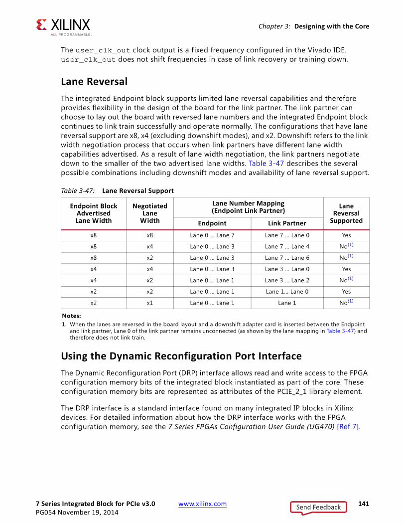
7 Series Integrated Block for PCIe v3.0 www.xilinx.com 141PG054 November 19, 2014
Chapter 3: Designing with the Core
The user_clk_out clock output is a f ixed frequency configured in the Vivado IDE. user_clk_out does not shift frequencies in case of link recovery or training down.
Lane ReversalThe integrated Endpoint block supports limited lane reversal capabilities and therefore provides flexibility in the design of the board for the link partner. The link partner can choose to lay out the board with reversed lane numbers and the integrated Endpoint block continues to link train successfully and operate normally. The configurations that have lane reversal support are x8, x4 (excluding downshift modes), and x2. Downshift refers to the link width negotiation process that occurs when link partners have different lane width capabilities advertised. As a result of lane width negotiation, the link partners negotiate down to the smaller of the two advertised lane widths. Table 3-47 describes the several possible combinations including downshift modes and availability of lane reversal support.
Using the Dynamic Reconfiguration Port InterfaceThe Dynamic Reconfiguration Port (DRP) interface allows read and write access to the FPGA configuration memory bits of the integrated block instantiated as part of the core. These configuration memory bits are represented as attributes of the PCIE_2_1 library element.
The DRP interface is a standard interface found on many integrated IP blocks in Xilinx devices. For detailed information about how the DRP interface works with the FPGA configuration memory, see the 7 Series FPGAs Configuration User Guide (UG470) [Ref 7].
Table 3-47: Lane Reversal Support
Endpoint BlockAdvertisedLane Width
NegotiatedLane
Width
Lane Number Mapping(Endpoint Link Partner) Lane
ReversalSupportedEndpoint Link Partner
x8 x8 Lane 0 ... Lane 7 Lane 7 ... Lane 0 Yes
x8 x4 Lane 0 ... Lane 3 Lane 7 ... Lane 4 No(1)
x8 x2 Lane 0 ... Lane 3 Lane 7 ... Lane 6 No(1)
x4 x4 Lane 0 ... Lane 3 Lane 3 ... Lane 0 Yes
x4 x2 Lane 0 ... Lane 1 Lane 3 ... Lane 2 No(1)
x2 x2 Lane 0 ... Lane 1 Lane 1... Lane 0 Yes
x2 x1 Lane 0 ... Lane 1 Lane 1 No(1)
Notes: 1. When the lanes are reversed in the board layout and a downshift adapter card is inserted between the Endpoint
and link partner, Lane 0 of the link partner remains unconnected (as shown by the lane mapping in Table 3-47) and therefore does not link train.
Send Feedback
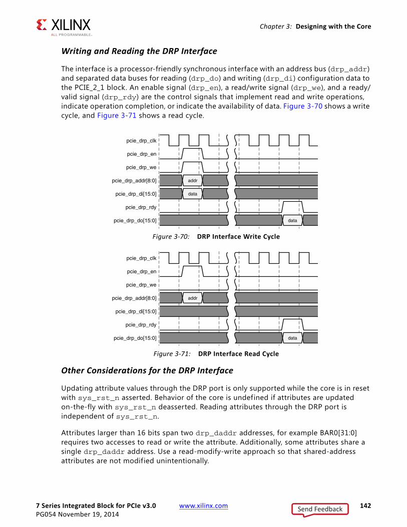
7 Series Integrated Block for PCIe v3.0 www.xilinx.com 142PG054 November 19, 2014
Chapter 3: Designing with the Core
Writing and Reading the DRP Interface
The interface is a processor-friendly synchronous interface with an address bus (drp_addr) and separated data buses for reading (drp_do) and writing (drp_di) configuration data to the PCIE_2_1 block. An enable signal (drp_en), a read/write signal (drp_we), and a ready/valid signal (drp_rdy) are the control signals that implement read and write operations, indicate operation completion, or indicate the availability of data. Figure 3-70 shows a write cycle, and Figure 3-71 shows a read cycle.
Other Considerations for the DRP Interface
Updating attribute values through the DRP port is only supported while the core is in reset with sys_rst_n asserted. Behavior of the core is undefined if attributes are updated on-the-fly with sys_rst_n deasserted. Reading attributes through the DRP port is independent of sys_rst_n.
Attributes larger than 16 bits span two drp_daddr addresses, for example BAR0[31:0] requires two accesses to read or write the attribute. Additionally, some attributes share a single drp_daddr address. Use a read-modify-write approach so that shared-address attributes are not modified unintentionally.
X-Ref Target - Figure 3-70
Figure 3-70: DRP Interface Write CycleX-Ref Target - Figure 3-71
Figure 3-71: DRP Interface Read Cycle
pcie_drp_clk
pcie_drp_en
pcie_drp_we
pcie_drp_addr[8:0]
pcie_drp_di[15:0]
pcie_drp_rdy
pcie_drp_do[15:0]
addr
data
data
pcie_drp_clk
pcie_drp_en
pcie_drp_we
pcie_drp_addr[8:0]
pcie_drp_di[15:0]
pcie_drp_rdy
pcie_drp_do[15:0]
addr
data
Send Feedback

7 Series Integrated Block for PCIe v3.0 www.xilinx.com 143PG054 November 19, 2014
Chapter 3: Designing with the Core
There are many attributes that should not be modified through DRP, because these attributes need to be set in an aligned manner with the rest of the design. For example, changing the memory latency attributes on the PCIE_2_1 block without changing the actual number of pipeline registers attached to the block RAM causes a functional failure. These attributes are included in this category:
• DEV_CAP_MAX_PAYLOAD_SUPPORTED
• VC0_TX_LASTPACKET
• TL_TX_RAM_RADDR_LATENCY
• TL_TX_RAM_RDATA_LATENCY
• TL_TX_RAM_WRITE_LATENCY
• VC0_RX_LIMIT
• TL_RX_RAM_RADDR_LATENCY
• TL_RX_RAM_RDATA_LATENCY
• TL_RX_RAM_WRITE_LATENCY
DRP Address Map
Table 3-48 defines the DRP address map for the PCIE_2_1 library element attributes. Some attributes span two addresses, for example, BAR0. In addition, some addresses contain multiple attributes; for example, address 0x004 contains both AER_CAP_NEXTPTR[11:0] and AER_CAP_ON.
Table 3-48: DRP Address Map for PCIE_2_1 Library Element Attributes
Attribute Name Address drp_daddr[8:0]
Data Bits drp_di[15:0] or drp_do[15:0]
AER_CAP_ECRC_CHECK_CAPABLE 0x000 [0]
AER_CAP_ECRC_GEN_CAPABLE 0x000 [1]
AER_CAP_ID[15:0] 0x001 [15:0]
AER_CAP_PERMIT_ROOTERR_UPDATE 0x002 [0]
AER_CAP_VERSION[3:0] 0x001 [4:1]
AER_BASE_PTR[11:0] 0x003 [11:0]
AER_CAP_NEXTPTR[11:0] 0x004 [11:0]
AER_CAP_ON 0x004 [12]
AER_CAP_OPTIONAL_ERR_SUPPORT[15:0] 0x005 [15:0]
AER_CAP_OPTIONAL_ERR_SUPPORT[23:16] 0x006 [7:0]
AER_CAP_MULTIHEADER 0x006 [8]
BAR0[15:0] 0x007 [15:0]
Send Feedback

7 Series Integrated Block for PCIe v3.0 www.xilinx.com 144PG054 November 19, 2014
Chapter 3: Designing with the Core
BAR0[31:16] 0x008 [15:0]
BAR1[15:0] 0x009 [15:0]
BAR1[31:16] 0x00a [15:0]
BAR2[15:0] 0x00b [15:0]
BAR2[31:16] 0x00c [15:0]
BAR3[15:0] 0x00d [15:0]
BAR3[31:16] 0x00e [15:0]
BAR4[15:0] 0x00f [15:0]
BAR4[31:16] 0x010 [15:0]
BAR5[15:0] 0x011 [15:0]
BAR5[31:16] 0x012 [15:0]
EXPANSION_ROM[15:0] 0x013 [15:0]
EXPANSION_ROM[31:16] 0x014 [15:0]
CAPABILITIES_PTR[7:0] 0x015 [7:0]
CARDBUS_CIS_POINTER[15:0] 0x016 [15:0]
CARDBUS_CIS_POINTER[31:16] 0x017 [15:0]
CLASS_CODE[15:0] 0x018 [15:0]
CLASS_CODE[23:16] 0x019 [7:0]
CMD_INTX_IMPLEMENTED 0x019 [8]
CPL_TIMEOUT_DISABLE_SUPPORTED 0x019 [9]
CPL_TIMEOUT_RANGES_SUPPORTED[3:0] 0x019 [13:10]
DEV_CAP2_ARI_FORWARDING_SUPPORTED 0x019 [14]
DEV_CAP2_ATOMICOP_ROUTING_SUPPORTED 0x019 [15]
DEV_CAP2_ATOMICOP32_COMPLETER_SUPPORTED 0x01a [0]
DEV_CAP2_ATOMICOP64_COMPLETER_SUPPORTED 0x01a [1]
DEV_CAP2_CAS128_COMPLETER_SUPPORTED 0x01a [2]
DEV_CAP2_NO_RO_ENABLED_PRPR_PASSING 0x01a [3]
DEV_CAP2_LTR_MECHANISM_SUPPORTED 0x01a [4]
DEV_CAP2_TPH_COMPLETER_SUPPORTED[1:0] 0x01a [6:5]
DEV_CAP2_EXTENDED_FMT_FIELD_SUPPORTED 0x01a [7]
DEV_CAP2_ENDEND_TLP_PREFIX_SUPPORTED 0x01a [8]
DEV_CAP2_MAX_ENDEND_TLP_PREFIXES[1:0] 0x01a [10:9]
ENDEND_TLP_PREFIX_FORWARDING_SUPPORTED 0x01a [11]
Table 3-48: DRP Address Map for PCIE_2_1 Library Element Attributes (Cont’d)
Attribute Name Address drp_daddr[8:0]
Data Bits drp_di[15:0] or drp_do[15:0]
Send Feedback
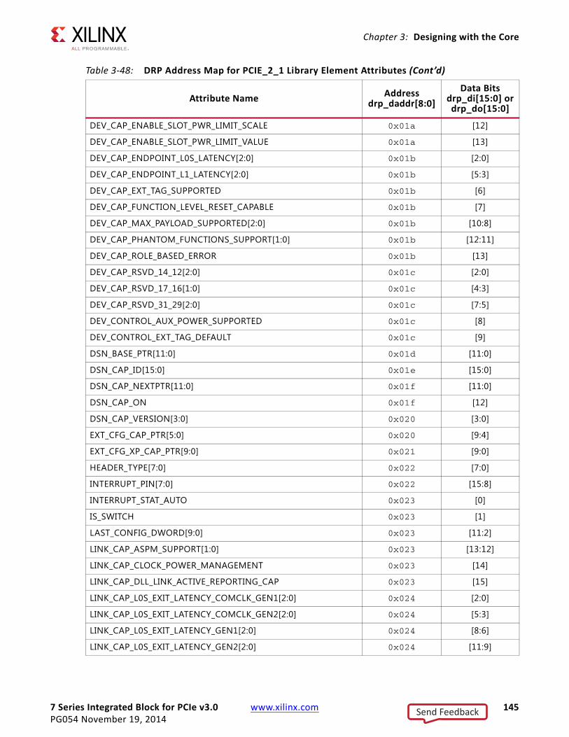
7 Series Integrated Block for PCIe v3.0 www.xilinx.com 145PG054 November 19, 2014
Chapter 3: Designing with the Core
DEV_CAP_ENABLE_SLOT_PWR_LIMIT_SCALE 0x01a [12]
DEV_CAP_ENABLE_SLOT_PWR_LIMIT_VALUE 0x01a [13]
DEV_CAP_ENDPOINT_L0S_LATENCY[2:0] 0x01b [2:0]
DEV_CAP_ENDPOINT_L1_LATENCY[2:0] 0x01b [5:3]
DEV_CAP_EXT_TAG_SUPPORTED 0x01b [6]
DEV_CAP_FUNCTION_LEVEL_RESET_CAPABLE 0x01b [7]
DEV_CAP_MAX_PAYLOAD_SUPPORTED[2:0] 0x01b [10:8]
DEV_CAP_PHANTOM_FUNCTIONS_SUPPORT[1:0] 0x01b [12:11]
DEV_CAP_ROLE_BASED_ERROR 0x01b [13]
DEV_CAP_RSVD_14_12[2:0] 0x01c [2:0]
DEV_CAP_RSVD_17_16[1:0] 0x01c [4:3]
DEV_CAP_RSVD_31_29[2:0] 0x01c [7:5]
DEV_CONTROL_AUX_POWER_SUPPORTED 0x01c [8]
DEV_CONTROL_EXT_TAG_DEFAULT 0x01c [9]
DSN_BASE_PTR[11:0] 0x01d [11:0]
DSN_CAP_ID[15:0] 0x01e [15:0]
DSN_CAP_NEXTPTR[11:0] 0x01f [11:0]
DSN_CAP_ON 0x01f [12]
DSN_CAP_VERSION[3:0] 0x020 [3:0]
EXT_CFG_CAP_PTR[5:0] 0x020 [9:4]
EXT_CFG_XP_CAP_PTR[9:0] 0x021 [9:0]
HEADER_TYPE[7:0] 0x022 [7:0]
INTERRUPT_PIN[7:0] 0x022 [15:8]
INTERRUPT_STAT_AUTO 0x023 [0]
IS_SWITCH 0x023 [1]
LAST_CONFIG_DWORD[9:0] 0x023 [11:2]
LINK_CAP_ASPM_SUPPORT[1:0] 0x023 [13:12]
LINK_CAP_CLOCK_POWER_MANAGEMENT 0x023 [14]
LINK_CAP_DLL_LINK_ACTIVE_REPORTING_CAP 0x023 [15]
LINK_CAP_L0S_EXIT_LATENCY_COMCLK_GEN1[2:0] 0x024 [2:0]
LINK_CAP_L0S_EXIT_LATENCY_COMCLK_GEN2[2:0] 0x024 [5:3]
LINK_CAP_L0S_EXIT_LATENCY_GEN1[2:0] 0x024 [8:6]
LINK_CAP_L0S_EXIT_LATENCY_GEN2[2:0] 0x024 [11:9]
Table 3-48: DRP Address Map for PCIE_2_1 Library Element Attributes (Cont’d)
Attribute Name Address drp_daddr[8:0]
Data Bits drp_di[15:0] or drp_do[15:0]
Send Feedback
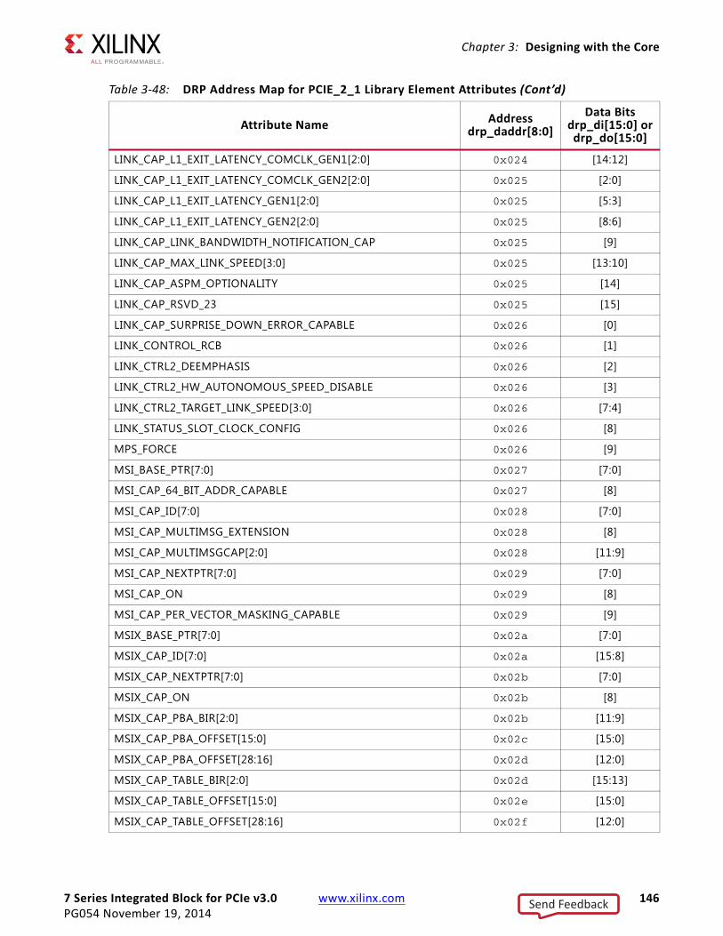
7 Series Integrated Block for PCIe v3.0 www.xilinx.com 146PG054 November 19, 2014
Chapter 3: Designing with the Core
LINK_CAP_L1_EXIT_LATENCY_COMCLK_GEN1[2:0] 0x024 [14:12]
LINK_CAP_L1_EXIT_LATENCY_COMCLK_GEN2[2:0] 0x025 [2:0]
LINK_CAP_L1_EXIT_LATENCY_GEN1[2:0] 0x025 [5:3]
LINK_CAP_L1_EXIT_LATENCY_GEN2[2:0] 0x025 [8:6]
LINK_CAP_LINK_BANDWIDTH_NOTIFICATION_CAP 0x025 [9]
LINK_CAP_MAX_LINK_SPEED[3:0] 0x025 [13:10]
LINK_CAP_ASPM_OPTIONALITY 0x025 [14]
LINK_CAP_RSVD_23 0x025 [15]
LINK_CAP_SURPRISE_DOWN_ERROR_CAPABLE 0x026 [0]
LINK_CONTROL_RCB 0x026 [1]
LINK_CTRL2_DEEMPHASIS 0x026 [2]
LINK_CTRL2_HW_AUTONOMOUS_SPEED_DISABLE 0x026 [3]
LINK_CTRL2_TARGET_LINK_SPEED[3:0] 0x026 [7:4]
LINK_STATUS_SLOT_CLOCK_CONFIG 0x026 [8]
MPS_FORCE 0x026 [9]
MSI_BASE_PTR[7:0] 0x027 [7:0]
MSI_CAP_64_BIT_ADDR_CAPABLE 0x027 [8]
MSI_CAP_ID[7:0] 0x028 [7:0]
MSI_CAP_MULTIMSG_EXTENSION 0x028 [8]
MSI_CAP_MULTIMSGCAP[2:0] 0x028 [11:9]
MSI_CAP_NEXTPTR[7:0] 0x029 [7:0]
MSI_CAP_ON 0x029 [8]
MSI_CAP_PER_VECTOR_MASKING_CAPABLE 0x029 [9]
MSIX_BASE_PTR[7:0] 0x02a [7:0]
MSIX_CAP_ID[7:0] 0x02a [15:8]
MSIX_CAP_NEXTPTR[7:0] 0x02b [7:0]
MSIX_CAP_ON 0x02b [8]
MSIX_CAP_PBA_BIR[2:0] 0x02b [11:9]
MSIX_CAP_PBA_OFFSET[15:0] 0x02c [15:0]
MSIX_CAP_PBA_OFFSET[28:16] 0x02d [12:0]
MSIX_CAP_TABLE_BIR[2:0] 0x02d [15:13]
MSIX_CAP_TABLE_OFFSET[15:0] 0x02e [15:0]
MSIX_CAP_TABLE_OFFSET[28:16] 0x02f [12:0]
Table 3-48: DRP Address Map for PCIE_2_1 Library Element Attributes (Cont’d)
Attribute Name Address drp_daddr[8:0]
Data Bits drp_di[15:0] or drp_do[15:0]
Send Feedback

7 Series Integrated Block for PCIe v3.0 www.xilinx.com 147PG054 November 19, 2014
Chapter 3: Designing with the Core
MSIX_CAP_TABLE_SIZE[10:0] 0x030 [10:0]
PCIE_BASE_PTR[7:0] 0x031 [7:0]
PCIE_CAP_CAPABILITY_ID[7:0] 0x031 [15:8]
PCIE_CAP_CAPABILITY_VERSION[3:0] 0x032 [3:0]
PCIE_CAP_DEVICE_PORT_TYPE[3:0] 0x032 [7:4]
PCIE_CAP_NEXTPTR[7:0] 0x032 [15:8]
PCIE_CAP_ON 0x033 [0]
PCIE_CAP_RSVD_15_14[1:0] 0x033 [2:1]
PCIE_CAP_SLOT_IMPLEMENTED 0x033 [3]
PCIE_REVISION[3:0] 0x033 [7:4]
PM_BASE_PTR[7:0] 0x033 [15:8]
PM_CAP_AUXCURRENT[2:0] 0x034 [2:0]
PM_CAP_D1SUPPORT 0x034 [3]
PM_CAP_D2SUPPORT 0x034 [4]
PM_CAP_DSI 0x034 [5]
PM_CAP_ID[7:0] 0x034 [13:6]
PM_CAP_NEXTPTR[7:0] 0x035 [7:0]
PM_CAP_ON 0x035 [8]
PM_CAP_PME_CLOCK 0x035 [9]
PM_CAP_PMESUPPORT[4:0] 0x035 [14:10]
PM_CAP_RSVD_04 0x035 [15]
PM_CAP_VERSION[2:0] 0x036 [2:0]
PM_CSR_B2B3 0x036 [3]
PM_CSR_BPCCEN 0x036 [4]
PM_CSR_NOSOFTRST 0x036 [5]
PM_DATA_SCALE0[1:0] 0x036 [7:6]
PM_DATA_SCALE1[1:0] 0x036 [9:8]
PM_DATA_SCALE2[1:0] 0x036 [11:10]
PM_DATA_SCALE3[1:0] 0x036 [13:12]
PM_DATA_SCALE4[1:0] 0x036 [15:14]
PM_DATA_SCALE5[1:0] 0x037 [1:0]
PM_DATA_SCALE6[1:0] 0x037 [3:2]
PM_DATA_SCALE7[1:0] 0x037 [5:4]
Table 3-48: DRP Address Map for PCIE_2_1 Library Element Attributes (Cont’d)
Attribute Name Address drp_daddr[8:0]
Data Bits drp_di[15:0] or drp_do[15:0]
Send Feedback

7 Series Integrated Block for PCIe v3.0 www.xilinx.com 148PG054 November 19, 2014
Chapter 3: Designing with the Core
PM_DATA0[7:0] 0x037 [13:6]
PM_DATA1[7:0] 0x038 [7:0]
PM_DATA2[7:0] 0x038 [15:8]
PM_DATA3[7:0] 0x039 [7:0]
PM_DATA4[7:0] 0x039 [15:8]
PM_DATA5[7:0] 0x03a [7:0]
PM_DATA6[7:0] 0x03a [15:8]
PM_DATA7[7:0] 0x03b [7:0]
RBAR_BASE_PTR[11:0] 0x03c [11:0]
RBAR_CAP_NEXTPTR[11:0] 0x03d [11:0]
RBAR_CAP_ON 0x03d [12]
RBAR_CAP_ID[15:0] 0x03e [15:0]
RBAR_CAP_VERSION[3:0] 0x03f [3:0]
RBAR_NUM[2:0] 0x03f [6:4]
RBAR_CAP_SUP0[15:0] 0x040 [15:0]
RBAR_CAP_SUP0[31:16] 0x041 [15:0]
RBAR_CAP_SUP1[15:0] 0x042 [15:0]
RBAR_CAP_SUP1[31:16] 0x043 [15:0]
RBAR_CAP_SUP2[15:0] 0x044 [15:0]
RBAR_CAP_SUP2[31:16] 0x045 [15:0]
RBAR_CAP_SUP3[15:0] 0x046 [15:0]
RBAR_CAP_SUP3[31:16] 0x047 [15:0]
RBAR_CAP_SUP4[15:0] 0x048 [15:0]
RBAR_CAP_SUP4[31:16] 0x049 [15:0]
RBAR_CAP_SUP5[15:0] 0x04a [15:0]
RBAR_CAP_SUP5[31:16] 0x04b [15:0]
RBAR_CAP_INDEX0[2:0] 0x04c [2:0]
RBAR_CAP_INDEX1[2:0] 0x04c [5:3]
RBAR_CAP_INDEX2[2:0] 0x04c [8:6]
RBAR_CAP_INDEX3[2:0] 0x04c [11:9]
RBAR_CAP_INDEX4[2:0] 0x04c [14:12]
RBAR_CAP_INDEX5[2:0] 0x04d [2:0]
RBAR_CAP_CONTROL_ENCODEDBAR0[4:0] 0x04d [7:3]
Table 3-48: DRP Address Map for PCIE_2_1 Library Element Attributes (Cont’d)
Attribute Name Address drp_daddr[8:0]
Data Bits drp_di[15:0] or drp_do[15:0]
Send Feedback

7 Series Integrated Block for PCIe v3.0 www.xilinx.com 149PG054 November 19, 2014
Chapter 3: Designing with the Core
RBAR_CAP_CONTROL_ENCODEDBAR1[4:0] 0x04d [12:8]
RBAR_CAP_CONTROL_ENCODEDBAR2[4:0] 0x04e [4:0]
RBAR_CAP_CONTROL_ENCODEDBAR3[4:0] 0x04e [9:5]
RBAR_CAP_CONTROL_ENCODEDBAR4[4:0] 0x04e [14:10]
RBAR_CAP_CONTROL_ENCODEDBAR5[4:0] 0x04f [4:0]
ROOT_CAP_CRS_SW_VISIBILITY 0x04f [5]
SELECT_DLL_IF 0x04f [6]
SLOT_CAP_ATT_BUTTON_PRESENT 0x04f [7]
SLOT_CAP_ATT_INDICATOR_PRESENT 0x04f [8]
SLOT_CAP_ELEC_INTERLOCK_PRESENT 0x04f [9]
SLOT_CAP_HOTPLUG_CAPABLE 0x04f [10]
SLOT_CAP_HOTPLUG_SURPRISE 0x04f [11]
SLOT_CAP_MRL_SENSOR_PRESENT 0x04f [12]
SLOT_CAP_NO_CMD_COMPLETED_SUPPORT 0x04f [13]
SLOT_CAP_PHYSICAL_SLOT_NUM[12:0] 0x050 [12:0]
SLOT_CAP_POWER_CONTROLLER_PRESENT 0x050 [13]
SLOT_CAP_POWER_INDICATOR_PRESENT 0x050 [14]
SLOT_CAP_SLOT_POWER_LIMIT_SCALE[1:0] 0x051 [1:0]
SLOT_CAP_SLOT_POWER_LIMIT_VALUE[7:0] 0x051 [9:2]
SSL_MESSAGE_AUTO 0x051 [10]
VC_BASE_PTR[11:0] 0x052 [11:0]
VC_CAP_NEXTPTR[11:0] 0x053 [11:0]
VC_CAP_ON 0x053 [12]
VC_CAP_ID[15:0] 0x054 [15:0]
VC_CAP_REJECT_SNOOP_TRANSACTIONS 0x055 [0]
VSEC_BASE_PTR[11:0] 0x055 [12:1]
VSEC_CAP_HDR_ID[15:0] 0x056 [15:0]
VSEC_CAP_HDR_LENGTH[11:0] 0x057 [11:0]
VSEC_CAP_HDR_REVISION[3:0] 0x057 [15:12]
VSEC_CAP_ID[15:0] 0x058 [15:0]
VSEC_CAP_IS_LINK_VISIBLE 0x059 [0]
VSEC_CAP_NEXTPTR[11:0] 0x059 [12:1]
VSEC_CAP_ON 0x059 [13]
Table 3-48: DRP Address Map for PCIE_2_1 Library Element Attributes (Cont’d)
Attribute Name Address drp_daddr[8:0]
Data Bits drp_di[15:0] or drp_do[15:0]
Send Feedback
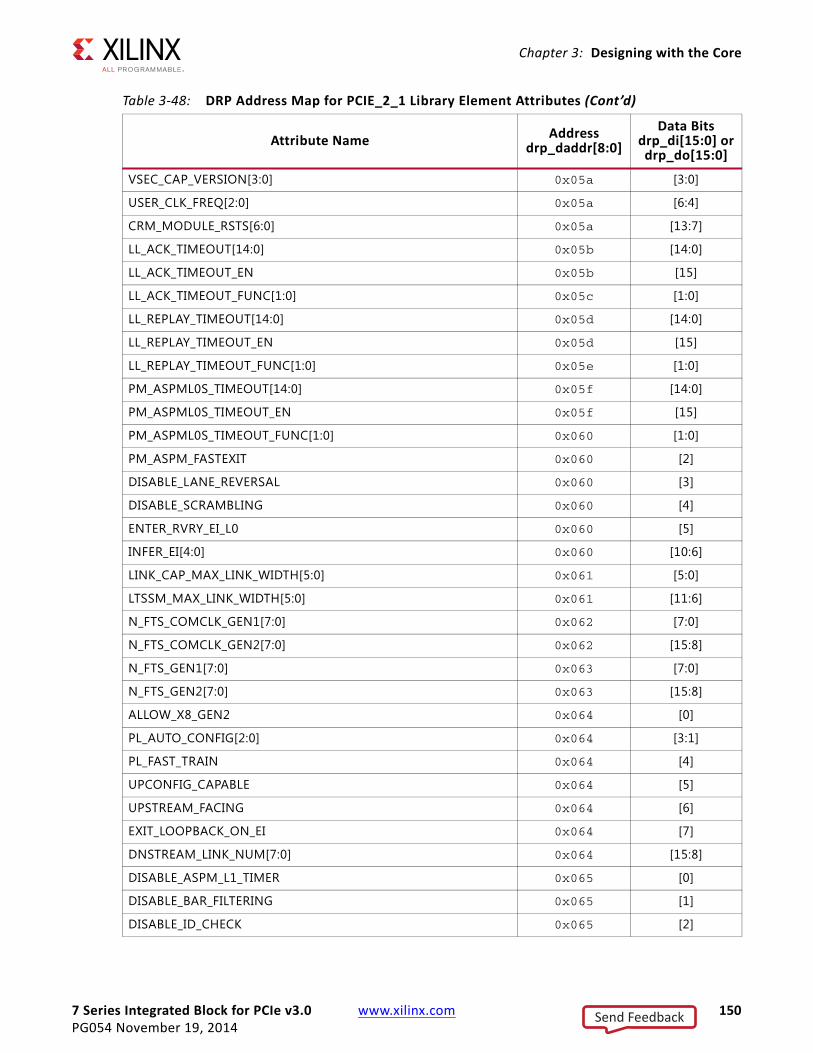
7 Series Integrated Block for PCIe v3.0 www.xilinx.com 150PG054 November 19, 2014
Chapter 3: Designing with the Core
VSEC_CAP_VERSION[3:0] 0x05a [3:0]
USER_CLK_FREQ[2:0] 0x05a [6:4]
CRM_MODULE_RSTS[6:0] 0x05a [13:7]
LL_ACK_TIMEOUT[14:0] 0x05b [14:0]
LL_ACK_TIMEOUT_EN 0x05b [15]
LL_ACK_TIMEOUT_FUNC[1:0] 0x05c [1:0]
LL_REPLAY_TIMEOUT[14:0] 0x05d [14:0]
LL_REPLAY_TIMEOUT_EN 0x05d [15]
LL_REPLAY_TIMEOUT_FUNC[1:0] 0x05e [1:0]
PM_ASPML0S_TIMEOUT[14:0] 0x05f [14:0]
PM_ASPML0S_TIMEOUT_EN 0x05f [15]
PM_ASPML0S_TIMEOUT_FUNC[1:0] 0x060 [1:0]
PM_ASPM_FASTEXIT 0x060 [2]
DISABLE_LANE_REVERSAL 0x060 [3]
DISABLE_SCRAMBLING 0x060 [4]
ENTER_RVRY_EI_L0 0x060 [5]
INFER_EI[4:0] 0x060 [10:6]
LINK_CAP_MAX_LINK_WIDTH[5:0] 0x061 [5:0]
LTSSM_MAX_LINK_WIDTH[5:0] 0x061 [11:6]
N_FTS_COMCLK_GEN1[7:0] 0x062 [7:0]
N_FTS_COMCLK_GEN2[7:0] 0x062 [15:8]
N_FTS_GEN1[7:0] 0x063 [7:0]
N_FTS_GEN2[7:0] 0x063 [15:8]
ALLOW_X8_GEN2 0x064 [0]
PL_AUTO_CONFIG[2:0] 0x064 [3:1]
PL_FAST_TRAIN 0x064 [4]
UPCONFIG_CAPABLE 0x064 [5]
UPSTREAM_FACING 0x064 [6]
EXIT_LOOPBACK_ON_EI 0x064 [7]
DNSTREAM_LINK_NUM[7:0] 0x064 [15:8]
DISABLE_ASPM_L1_TIMER 0x065 [0]
DISABLE_BAR_FILTERING 0x065 [1]
DISABLE_ID_CHECK 0x065 [2]
Table 3-48: DRP Address Map for PCIE_2_1 Library Element Attributes (Cont’d)
Attribute Name Address drp_daddr[8:0]
Data Bits drp_di[15:0] or drp_do[15:0]
Send Feedback

7 Series Integrated Block for PCIe v3.0 www.xilinx.com 151PG054 November 19, 2014
Chapter 3: Designing with the Core
DISABLE_RX_TC_FILTER 0x065 [3]
DISABLE_RX_POISONED_RESP 0x065 [4]
ENABLE_MSG_ROUTE[10:0] 0x065 [15:5]
ENABLE_RX_TD_ECRC_TRIM 0x066 [0]
TL_RX_RAM_RADDR_LATENCY 0x066 [1]
TL_RX_RAM_RDATA_LATENCY[1:0] 0x066 [3:2]
TL_RX_RAM_WRITE_LATENCY 0x066 [4]
TL_TFC_DISABLE 0x066 [5]
TL_TX_CHECKS_DISABLE 0x066 [6]
TL_RBYPASS 0x066 [7]
DISABLE_PPM_FILTER 0x066 [8]
DISABLE_LOCKED_FILTER 0x066 [9]
USE_RID_PINS 0x066 [10]
DISABLE_ERR_MSG 0x066 [11]
PM_MF 0x066 [12]
TL_TX_RAM_RADDR_LATENCY 0x066 [13]
TL_TX_RAM_RDATA_LATENCY[1:0] 0x066 [15:14]
TL_TX_RAM_WRITE_LATENCY 0x067 [0]
VC_CAP_VERSION[3:0] 0x067 [4:1]
VC0_CPL_INFINITE 0x067 [5]
VC0_RX_RAM_LIMIT[12:0] 0x068 [12:0]
VC0_TOTAL_CREDITS_CD[10:0] 0x069 [10:0]
VC0_TOTAL_CREDITS_CH[6:0] 0x06a [6:0]
VC0_TOTAL_CREDITS_NPH[6:0] 0x06a [13:7]
VC0_TOTAL_CREDITS_NPD[10:0] 0x06b [10:0]
VC0_TOTAL_CREDITS_PD[10:0] 0x06c [10:0]
VC0_TOTAL_CREDITS_PH[6:0] 0x06d [6:0]
VC0_TX_LASTPACKET[4:0] 0x06d [11:7]
RECRC_CHK[1:0] 0x06d [13:12]
RECRC_CHK_TRIM 0x06d [14]
TECRC_EP_INV 0x06d [15]
CFG_ECRC_ERR_CPLSTAT[1:0] 0x06e [1:0]
UR_INV_REQ 0x06e [2]
Table 3-48: DRP Address Map for PCIE_2_1 Library Element Attributes (Cont’d)
Attribute Name Address drp_daddr[8:0]
Data Bits drp_di[15:0] or drp_do[15:0]
Send Feedback
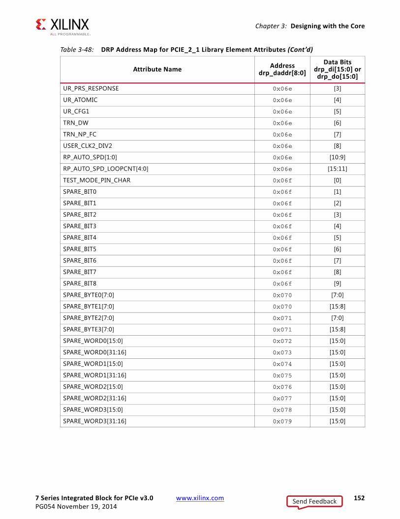
7 Series Integrated Block for PCIe v3.0 www.xilinx.com 152PG054 November 19, 2014
Chapter 3: Designing with the Core
UR_PRS_RESPONSE 0x06e [3]
UR_ATOMIC 0x06e [4]
UR_CFG1 0x06e [5]
TRN_DW 0x06e [6]
TRN_NP_FC 0x06e [7]
USER_CLK2_DIV2 0x06e [8]
RP_AUTO_SPD[1:0] 0x06e [10:9]
RP_AUTO_SPD_LOOPCNT[4:0] 0x06e [15:11]
TEST_MODE_PIN_CHAR 0x06f [0]
SPARE_BIT0 0x06f [1]
SPARE_BIT1 0x06f [2]
SPARE_BIT2 0x06f [3]
SPARE_BIT3 0x06f [4]
SPARE_BIT4 0x06f [5]
SPARE_BIT5 0x06f [6]
SPARE_BIT6 0x06f [7]
SPARE_BIT7 0x06f [8]
SPARE_BIT8 0x06f [9]
SPARE_BYTE0[7:0] 0x070 [7:0]
SPARE_BYTE1[7:0] 0x070 [15:8]
SPARE_BYTE2[7:0] 0x071 [7:0]
SPARE_BYTE3[7:0] 0x071 [15:8]
SPARE_WORD0[15:0] 0x072 [15:0]
SPARE_WORD0[31:16] 0x073 [15:0]
SPARE_WORD1[15:0] 0x074 [15:0]
SPARE_WORD1[31:16] 0x075 [15:0]
SPARE_WORD2[15:0] 0x076 [15:0]
SPARE_WORD2[31:16] 0x077 [15:0]
SPARE_WORD3[15:0] 0x078 [15:0]
SPARE_WORD3[31:16] 0x079 [15:0]
Table 3-48: DRP Address Map for PCIE_2_1 Library Element Attributes (Cont’d)
Attribute Name Address drp_daddr[8:0]
Data Bits drp_di[15:0] or drp_do[15:0]
Send Feedback

7 Series Integrated Block for PCIe v3.0 www.xilinx.com 153PG054 November 19, 2014
Chapter 3: Designing with the Core
Tandem ConfigurationThe 7 Series Gen2 Integrated Block for PCIe solution provides two alternative configuration methods to meet the time requirements indicated within the PCI Express Specif ication. The PCI Express Specification states that PERST# must deassert 100 ms after the power good of the systems has occurred, and a PCI Express port must be ready to link train no more than 20ms after PERST# has deasserted. This is commonly referred to as the 100 ms boot time requirement. The two alternative methods for configuration are referred to as Tandem PROM and Tandem PCI Express (PCIe). These solutions have been explicitly designed for this specific goal. If other configuration flexibility is needed, such as dynamic f ield updates of the user application, general Partial Reconfiguration should be used instead of Tandem Configuration.
Both Tandem PROM and Tandem PCIe implement a two stage configuration methodology. In Tandem PROM and Tandem PCIe, the f irst stage configuration memory cells that are critical to PCI Express operation are loaded through a local PROM. When these cells have been loaded, an FPGA start-up command is sent at the end of the f irst stage bitstream to the FPGA configuration controller. The partially configured FPGA then becomes active with the first-stage bitstream contents. The f irst stage containing a fully functional PCI Express port responds to traff ic received during PCI Express enumeration while the second stage is loaded into the FPGA. Included inside the first stage bitstream are the PCI Express integrated block, Gigabit Transceivers, block RAM, clocking resources, FPGA logic, and routing resources required to make the entire PCI Express port functional. The second stage consists of the user-specif ic application and the remaining clocking and I/O resources, which is basically the rest of the FPGA design. The mechanism for loading the second stage bitstream differs between Tandem PROM and Tandem PCIe.
Supported DevicesThe 7 Series Gen2 Integrated Block for PCIe core and Vivado tool flow support implementations targeting Xilinx reference boards and specific part/package combinations.
For the Vivado Design Suite 2014.4 release, Tandem Configuration is production for specif ic devices and packages only. Tandem Configuration supports the configurations found in Table 3-49.
Table 3-49: Tandem PROM/PCIe Supported Configurations
HDL Verilog Only
PCIe Configuration All configurations (max: X8Gen2)
Xilinx Reference Board SupportKC705 Evaluation Board for Kintex®-7 FPGA VC707 Evaluation Board for Virtex®-7 FPGAZC706 Evaluation Board for Zynq® SOC
Send Feedback
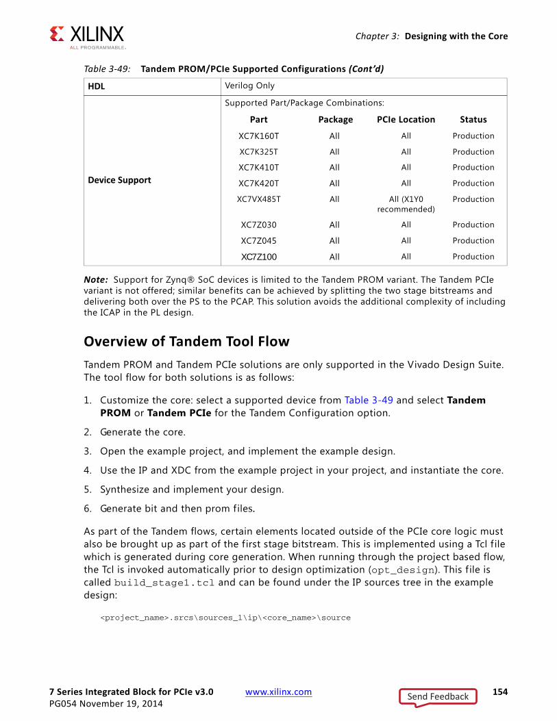
7 Series Integrated Block for PCIe v3.0 www.xilinx.com 154PG054 November 19, 2014
Chapter 3: Designing with the Core
Note: Support for Zynq® SoC devices is limited to the Tandem PROM variant. The Tandem PCIe variant is not offered; similar benefits can be achieved by splitting the two stage bitstreams and delivering both over the PS to the PCAP. This solution avoids the additional complexity of including the ICAP in the PL design.
Overview of Tandem Tool FlowTandem PROM and Tandem PCIe solutions are only supported in the Vivado Design Suite. The tool flow for both solutions is as follows:
1. Customize the core: select a supported device from Table 3-49 and select Tandem PROM or Tandem PCIe for the Tandem Configuration option.
2. Generate the core.
3. Open the example project, and implement the example design.
4. Use the IP and XDC from the example project in your project, and instantiate the core.
5. Synthesize and implement your design.
6. Generate bit and then prom files.
As part of the Tandem flows, certain elements located outside of the PCIe core logic must also be brought up as part of the f irst stage bitstream. This is implemented using a Tcl f ile which is generated during core generation. When running through the project based flow, the Tcl is invoked automatically prior to design optimization (opt_design). This f ile is called build_stage1.tcl and can be found under the IP sources tree in the example design:
<project_name>.srcs\sources_1\ip\<core_name>\source
Device Support
Supported Part/Package Combinations:
Part Package PCIe Location Status
XC7K160T All All Production
XC7K325T All All Production
XC7K410T All All Production
XC7K420T All All Production
XC7VX485T All All (X1Y0 recommended)
Production
XC7Z030 All All Production
XC7Z045 All All Production
XC7Z100 All All Production
Table 3-49: Tandem PROM/PCIe Supported Configurations (Cont’d)
HDL Verilog Only
Send Feedback
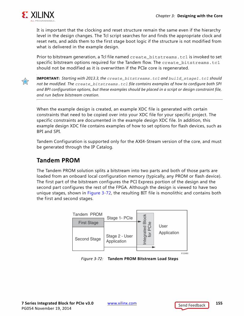
7 Series Integrated Block for PCIe v3.0 www.xilinx.com 155PG054 November 19, 2014
Chapter 3: Designing with the Core
It is important that the clocking and reset structure remain the same even if the hierarchy level in the design changes. The Tcl script searches for and finds the appropriate clock and reset nets, and adds them to the first stage boot logic if the structure is not modified from what is delivered in the example design.
Prior to bitstream generation, a Tcl f ile named create_bitstreams.tcl is invoked to set specific bitstream options required for the Tandem flow. The create_bitstreams.tcl should not be modified as it is overwritten if the PCIe core is regenerated.
IMPORTANT: Starting with 2013.3, the create_bitstreams.tcl and build_stage1.tcl should not be modified. The create_bitstreams.tcl file contains examples of how to configure both SPI and BPI configuration options, but these examples should be placed in a script or design constraint file, and run before bitstream creation.
When the example design is created, an example XDC file is generated with certain constraints that need to be copied over into your XDC file for your specif ic project. The specific constraints are documented in the example design XDC file. In addition, this example design XDC file contains examples of how to set options for flash devices, such as BPI and SPI.
Tandem Configuration is supported only for the AXI4-Stream version of the core, and must be generated through the IP Catalog.
Tandem PROM The Tandem PROM solution splits a bitstream into two parts and both of those parts are loaded from an onboard local configuration memory (typically, any PROM or flash device). The first part of the bitstream configures the PCI Express portion of the design and the second part configures the rest of the FPGA. Although the design is viewed to have two unique stages, shown in Figure 3-72, the resulting BIT f ile is monolithic and contains both the first and second stages.
X-Ref Target - Figure 3-72
Figure 3-72: Tandem PROM Bitstream Load Steps
Send Feedback
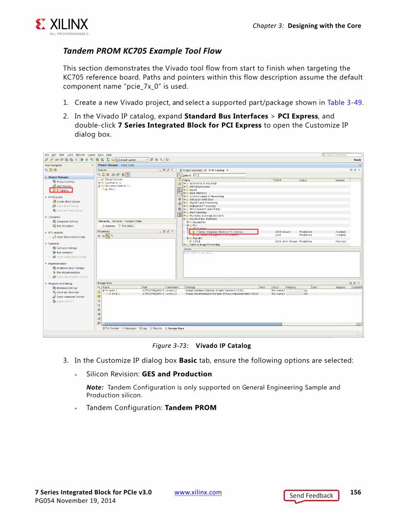
7 Series Integrated Block for PCIe v3.0 www.xilinx.com 156PG054 November 19, 2014
Chapter 3: Designing with the Core
Tandem PROM KC705 Example Tool Flow
This section demonstrates the Vivado tool flow from start to f inish when targeting the KC705 reference board. Paths and pointers within this flow description assume the default component name “pcie_7x_0” is used.
1. Create a new Vivado project, and select a supported part/package shown in Table 3-49.
2. In the Vivado IP catalog, expand Standard Bus Interfaces > PCI Express, and double-click 7 Series Integrated Block for PCI Express to open the Customize IP dialog box.
3. In the Customize IP dialog box Basic tab, ensure the following options are selected:
° Silicon Revision: GES and Production
Note: Tandem Configuration is only supported on General Engineering Sample and Production silicon.
° Tandem Configuration: Tandem PROM
X-Ref Target - Figure 3-73
Figure 3-73: Vivado IP Catalog
Send Feedback

7 Series Integrated Block for PCIe v3.0 www.xilinx.com 157PG054 November 19, 2014
Chapter 3: Designing with the Core
4. Perform additional PCIe customizations, and click OK to generate the core.
5. Click Generate when asked about which Output Products to create.
6. In the Sources tab, right-click the core, and select Open IP Example Design.
A new instance of Vivado is created and the example design is automatically loaded into the Vivado IDE.
7. Run Synthesis and Implementation.
Click Run Implementation in the Flow Navigator. Select OK to run through synthesis f irst. The design runs through the complete tool flow and the result is a fully routed design that supports Tandem PROM.
8. Setup PROM or Flash settings.
Set the appropriate settings to correctly generate a bitstream for a PROM or Flash device. For more information, see Programming the Device, page 170.
9. Generate the bitstream.
X-Ref Target - Figure 3-74
Figure 3-74: Tandem PROM
Send Feedback

7 Series Integrated Block for PCIe v3.0 www.xilinx.com 158PG054 November 19, 2014
Chapter 3: Designing with the Core
After Synthesis and Implementation is complete, click Generate Bitstream in the Flow Navigator. A bitstream supporting Tandem configuration is generated in the runs directory, for example: ./pcie_7x_0_example.runs/impl/xilinx_pcie_2_2_ep_7x.bit.
Note: You have the option of creating the f irst and second stage bitstreams independently. This flow allows you to control the loading of each stage through the JTAG interface for testing purposes. Here are the commands required to generate the bitstreams. This command can be seen in the create_bitstreams.tcl f ile, and can be added to a Tcl script f ile and included as a tcl.pre f ile for the Write Bitstream step. This can be done through the Bitstream Settings dialog box under the “tcl.pre” setting.
set_property bitstream.config.tandem_writebitstream separate [current_design]
The resulting bit f iles created are named xilinx_pcie_2_2_ep_7x_tandem1.bit and xilinx_pcie_2_2_ep_7x_tandem2.bit.
10. Generate the PROM file.
Run the following command in the Vivado Tcl Console to create a PROM file supported on the KC705 development board.
promgen -w -p mcs -spi -u 0x0 xilinx_pcie_2_2_ep_7x.bit
Tandem PROM Summary
By using Tandem PROM, you can signif icantly reduce the amount of time required to configure the PCIe portion of a 7 series FPGA design. The 7 Series Gen2 Integrated Block for PCIe core manages many design details, allowing you to focus your attention on the user application.
Tandem PCIeTandem PCIe is similar to Tandem PROM. In the f irst stage bitstream, only the conf iguration memory cells that are necessary for PCI Express operation are loaded from the PROM. After the first stage bitstream is loaded, the PCI Express port is capable of responding to enumeration traff ic. Subsequently, the second stage of the bitstream is transmitted through the PCI Express link . Figure 3-75 illustrates the bitstream loading flow.
Send Feedback

7 Series Integrated Block for PCIe v3.0 www.xilinx.com 159PG054 November 19, 2014
Chapter 3: Designing with the Core
Tandem PCIe is similar to the standard model used today in terms of tool flow and bitstream generation. Two bitstreams are produced when running bitstream generation. One BIT f ile representing the f irst stage is downloaded into the PROM while the other BIT f ile representing the user application (the second stage) configures the remainder of the FPGA using the Internal Configuration Access Port (ICAP).
Note: Field updates of the second stage bitstream, that is, multiple user application images for an unchanging f irst stage bitstream, require partial reconfiguration, which is not yet a supported flow. If this capability is required, a standard partial reconfiguration flow, utilizing a black box configuration and compression, should be used.
Tandem PCIe KC705 Example Tool Flow
This section demonstrates the Vivado tool flow from start to f inish when targeting the KC705 reference board. Paths and pointers within this flow description assume the default component name pcie_7x_0 is used.
1. When creating a new Vivado project, select a supported part/package shown in Table 3-49.
2. In the Vivado IP catalog, expand Standard Bus Interfaces > PCI Express, and double-click 7 Series Integrated Block for PCI Express to open the Customize IP dialog box.
X-Ref Target - Figure 3-75
Figure 3-75: Tandem PCIe Bitstream Load Steps
Send Feedback
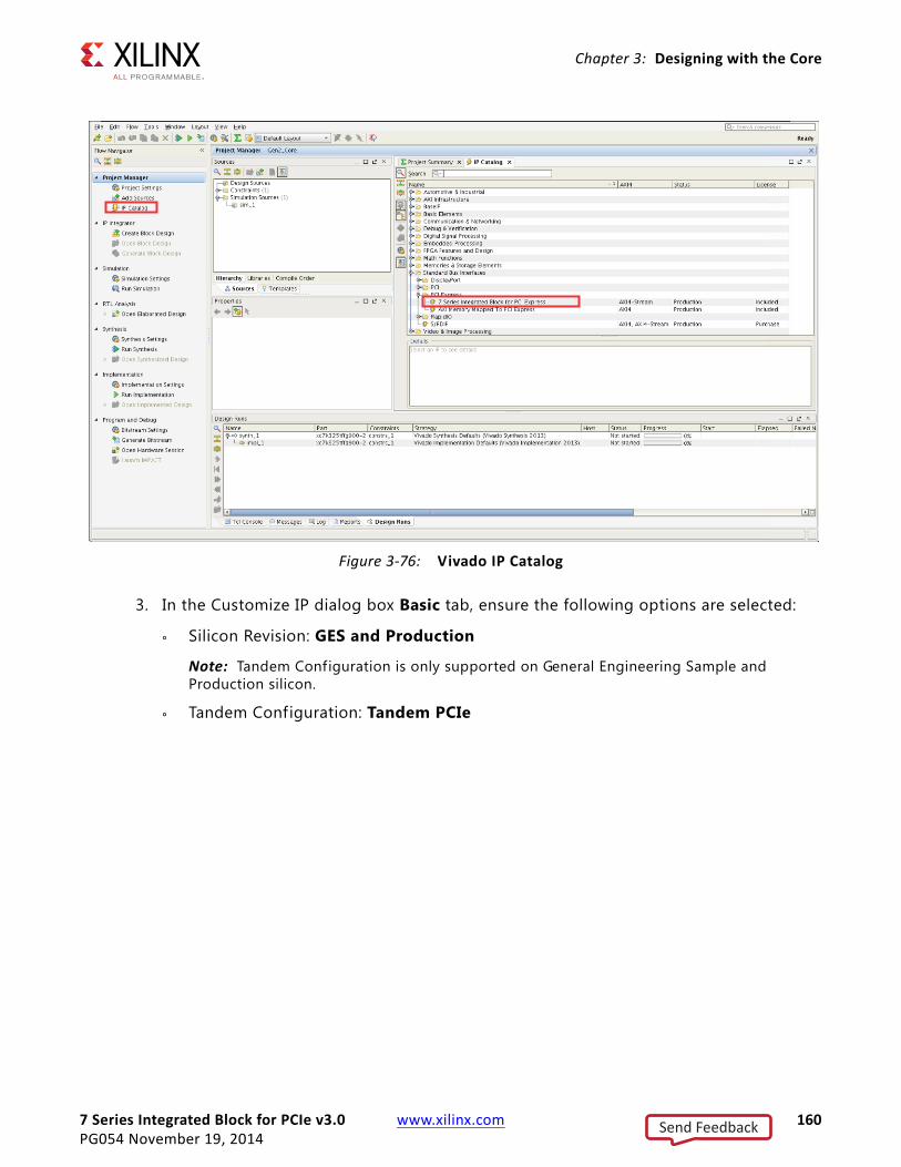
7 Series Integrated Block for PCIe v3.0 www.xilinx.com 160PG054 November 19, 2014
Chapter 3: Designing with the Core
3. In the Customize IP dialog box Basic tab, ensure the following options are selected:
° Silicon Revision: GES and Production
Note: Tandem Configuration is only supported on General Engineering Sample and Production silicon.
° Tandem Configuration: Tandem PCIe
X-Ref Target - Figure 3-76
Figure 3-76: Vivado IP Catalog
Send Feedback
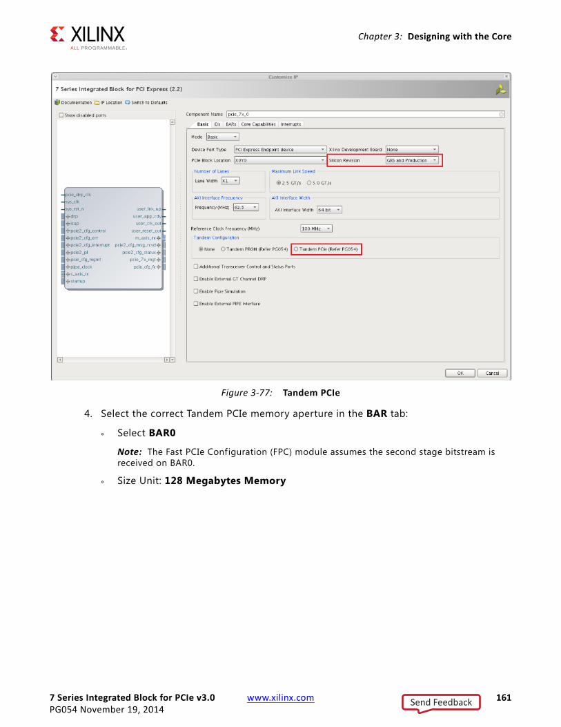
7 Series Integrated Block for PCIe v3.0 www.xilinx.com 161PG054 November 19, 2014
Chapter 3: Designing with the Core
4. Select the correct Tandem PCIe memory aperture in the BAR tab:
° Select BAR0
Note: The Fast PCIe Configuration (FPC) module assumes the second stage bitstream is received on BAR0.
° Size Unit: 128 Megabytes Memory
X-Ref Target - Figure 3-77
Figure 3-77: Tandem PCIe
Send Feedback
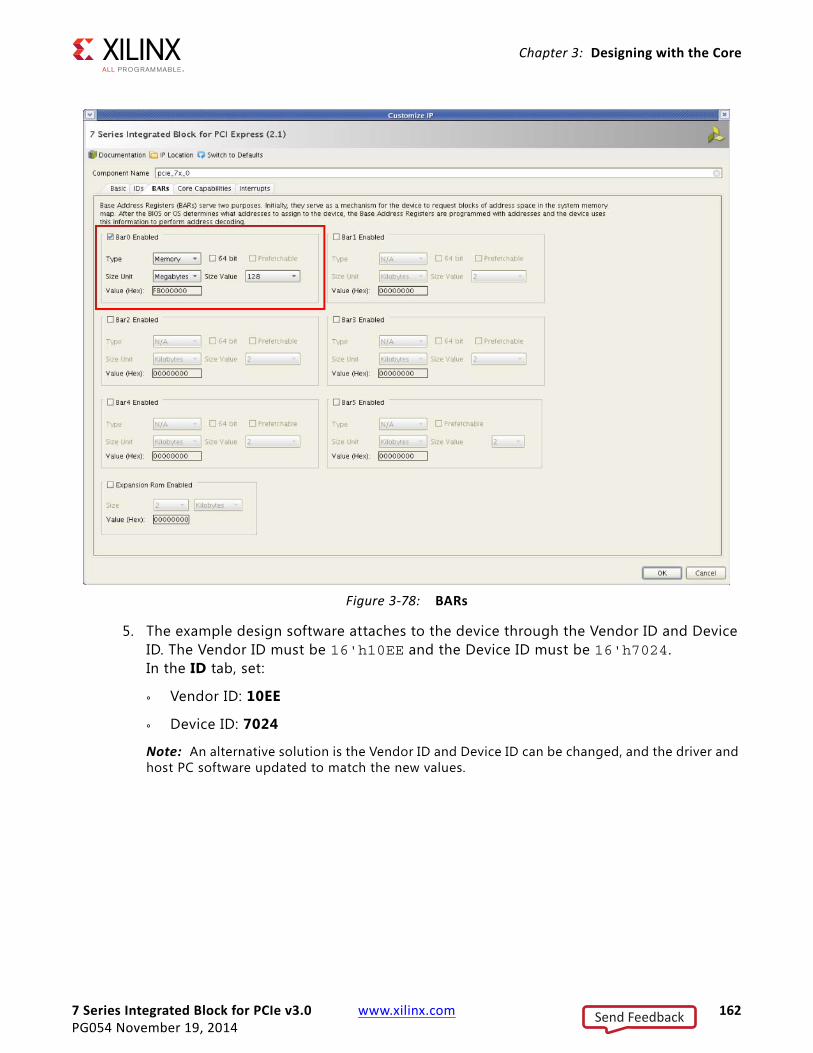
7 Series Integrated Block for PCIe v3.0 www.xilinx.com 162PG054 November 19, 2014
Chapter 3: Designing with the Core
5. The example design software attaches to the device through the Vendor ID and Device ID. The Vendor ID must be 16'h10EE and the Device ID must be 16'h7024. In the ID tab, set:
° Vendor ID: 10EE
° Device ID: 7024
Note: An alternative solution is the Vendor ID and Device ID can be changed, and the driver and host PC software updated to match the new values.
X-Ref Target - Figure 3-78
Figure 3-78: BARs
Send Feedback
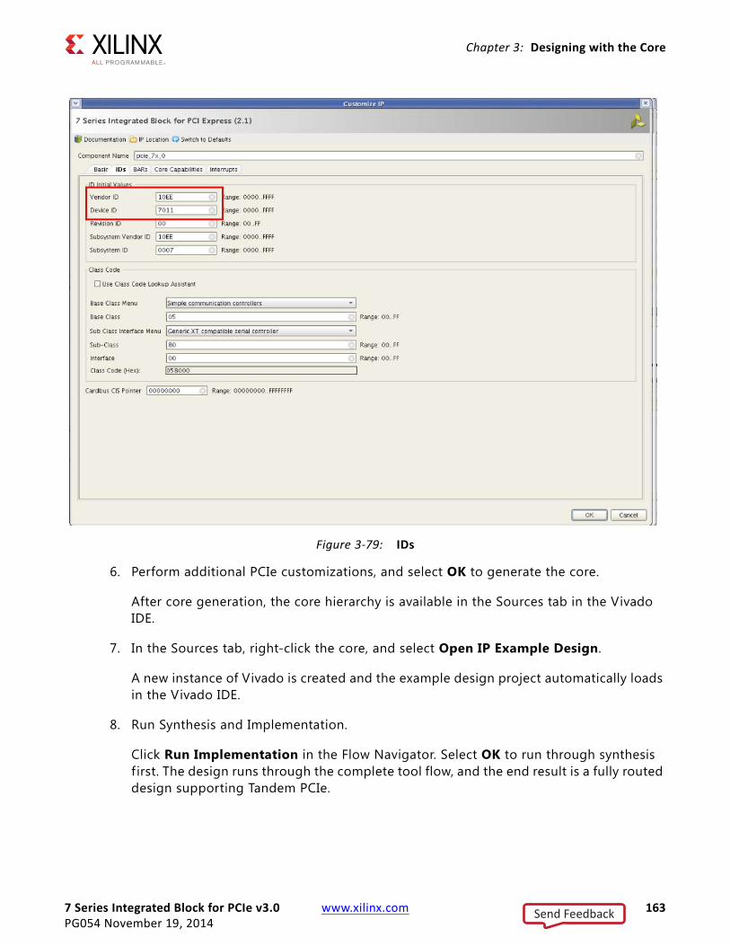
7 Series Integrated Block for PCIe v3.0 www.xilinx.com 163PG054 November 19, 2014
Chapter 3: Designing with the Core
6. Perform additional PCIe customizations, and select OK to generate the core.
After core generation, the core hierarchy is available in the Sources tab in the Vivado IDE.
7. In the Sources tab, right-click the core, and select Open IP Example Design.
A new instance of Vivado is created and the example design project automatically loads in the Vivado IDE.
8. Run Synthesis and Implementation.
Click Run Implementation in the Flow Navigator. Select OK to run through synthesis f irst. The design runs through the complete tool flow, and the end result is a fully routed design supporting Tandem PCIe.
X-Ref Target - Figure 3-79
Figure 3-79: IDs
Send Feedback
7 Series Integrated Block for PCIe v3.0 www.xilinx.com 164PG054 November 19, 2014
Chapter 3: Designing with the Core
9. Setup PROM or Flash settings.
Set the appropriate settings to correctly generate a bitstream for a PROM or Flash device. For more information, see Programming the Device, page 170.
10. Generate the bitstream.
After Synthesis and Implementation are complete, click Generate Bitstream in the Flow Navigator. The following four f iles are created and placed in the runs directory:
xilinx_pcie_2_2_ep_7x_tandem1.bit|xilinx_pcie_2_2_ep_7x_tandem2.bit|xilinx_pcie_2_2_ep_7x_tandem1.bin|xilinx_pcie_2_2_ep_7x_tandem2.bin
The .bit f iles allow you to control the loading of each stage through the JTAG interface. The second stage .bin f ile is 32-bit word aligned and should be used to load the second stage configuration through the PCIe interface.
11. Generate the PROM file for the f irst stage.
Run the following command in the Vivado Tcl Console to create a PROM file supported on the KC705 development board.
promgen -w -p mcs -spi -u 0x0 xilinx_pcie_2_2_ep_7x_tandem1.bit
Loading The Second Stage Through PCI Express
An example kernel mode driver and user space application is provided with the IP. For information on retrieving the software and documentation, see AR 51950.
Tandem PCIe Summary
By using Tandem PCIe, you can signif icantly reduce the amount of time required for configuration of the PCIe portion of a 7 series design, and can reduce the bitstream flash storage requirements. The 7 Series Gen2 Integrated Block for PCIe core manages many design details, allowing you to focus your attention on the user application.
Using Tandem With a User Hardware DesignThere are two methods available to apply the Tandem flow to a user design. The first method is to use the example design that comes with the core. The second method is to import the PCIe IP into an existing design and change the hierarchy of the design if required.
Regardless of which method you use, the PCIe example design should be created to get the example clocking structure, timing constraints, and physical block (Pblock) constraints needed for the Tandem solution.
Send Feedback

7 Series Integrated Block for PCIe v3.0 www.xilinx.com 165PG054 November 19, 2014
Chapter 3: Designing with the Core
Method 1 – Using the Existing PCI Express Example Design
This is the simplest method in terms of what must be done with the PCI Express core, but might not be feasible for all users. If this approach meets your design structure needs, follow these steps.
1. Create the example design.
Generate the example design as described in the Tandem PROM KC705 Example Tool Flow and Tandem PCIe KC705 Example Tool Flow.
2. Insert the user application.
Replace the PIO example design with the user design. It is recommended that the global and top-level elements, such as I/O and global clocking, be inserted in the top-level design.
3. Copy the appropriate SPI or BPI settings from the create_bitstream.tcl f ile and paste them in a new Tcl f ile.
4. Update the Vivado settings to run this Tcl f ile before the bitstream is generated. Implement the design as normal.
Method 2 – Migrating the PCIe Design into a New Vivado Project
In cases where it is not possible to use method one above, the following steps should be followed to use the PCIe core and the desired Tandem flow (PROM or PCIe) in a new project. The example project has many of the required RTL and scripts that must be migrated into the user design.
1. Create the example design.
Generate the example design as described in the Tandem PROM KC705 Example Tool Flow and Tandem PCIe KC705 Example Tool Flow.
2. Migrate the clock module.
If the Include Shared Logic (Clocking) in the example design option is set in the Shared Logic tab during core generation, then the pipe_clock_i clock module is instantiated in the top level of the example design. This clock module should be migrated to the user design to provide the necessary PCIe clocks.
Note: These clocks can be used in other parts of the user design if desired.
3. Migrate the top-level constraint.
The example Xilinx design constraints (XDC) f ile contains timing constraints, location constraints and Pblock constraints for the PCIe core. All of these constraints (other than the I/O location and I/O standard constraints) need to be migrated to the user design.
Send Feedback
7 Series Integrated Block for PCIe v3.0 www.xilinx.com 166PG054 November 19, 2014
Chapter 3: Designing with the Core
Several of the constraints contain hierarchical references that require updating if the hierarchy of the design is different than the example design.
4. Migrate the top-level Pblock constraint.
The following constraint is easy to miss so it is called out specif ically in this step. The Pblock constraint should point to the top level of the PCIe core.
add_cells_to_pblock [get_pblocks main_pblock_boot] [get_cells -quiet [<path>]]
IMPORTANT: Do not make any changes to the physical constraints defined in the XDC file because the constraints are device dependent.
5. Add the Tandem PCIe IP to the Vivado project.
Click Add Sources in the Flow Navigator. In the Add Source wizard, select Add Existing IP and then browse to the XCI f ile that was used to create the Tandem PCIe example design.
6. Copy the appropriate SPI or BPI settings from the example design XDC file and paste them in your design XDC file.
Update the Vivado settings to run this Tcl f ile before the bitstream is generated.
7. Implement the design as normal.
Tandem Configuration RTL DesignTandem Configuration requires slight modif ications from the non-tandem PCI Express product. This section indicates the additional logic integrated within the core and the additional responsibilities of the user application to implement a Tandem PROM solution.
MUXing Critical Inputs
Certain input ports to the core are multiplexed so that they are disabled during the second stage configuration process. These MUXes are located in the top-level core file and are controlled by the user_app_rdy signal.
These inputs are held in a deasserted state while the second stage bitstream is loaded. This masks off any unwanted glitching due to the absence of second stage drivers and keeps the PCIe core in a valid state. When user_app_rdy is asserted, the MUXes are switched, and all interface signals behave as described in this document.
Tandem Completer
In addition to receiving configuration request packets, the PCI Express endpoint might receive TLP requests that are not processed within the PCI Express hard block. Typical TLP requests received are Vendor Defined Messages and Read Requests. To avoid a lockup
Send Feedback
7 Series Integrated Block for PCIe v3.0 www.xilinx.com 167PG054 November 19, 2014
Chapter 3: Designing with the Core
scenario within the PCI Express IP, TLP requests must be drained from the core to allow Configuration requests to be completed successfully.
A completer module is implemented when a Tandem mode is selected to process these packets. A Tandem Fast PCIe Configuration (FPC) module is implemented to process these packets. All read requests are expected to be 1DW and a CPLD is returned with a payload of 32’h0. All Vendor Defined Message requests are purged from the cores receive buffer and no further processing is performed. Each Memory Write request targeting BAR0 is processed by the FPC and assumed to be second stage bitstream data. The payload is forwarded to the ICAP. After the second stage bitstream is loaded and user_app_rdy asserted, the Tandem FPC module becomes inactive.
Tandem Configuration Logic
The core and example design contain ports (signals) specif ic to Tandem Configuration. These signals provide handshaking between the f irst stage (the core) and the second stage (user logic). Handshaking is necessary for interaction between the core and the user logic. Table 3-50 defines the handshaking ports on the core.
These signals can coordinate events in the user application, such as the release of output 3-state buffers described in Tandem Configuration Details. Here is some additional information about these signals:
• user_app_rdy is asserted 2 to 12 clock cycles after stage two is loaded. The delay ensures that user_app_rdy is not asserted in the middle of a PCIe transaction.
• user_reset can likewise be used to reset any logic that communicates with the core when the core itself is reset.
• user_clk is simply the main internal clock for the PCIe IP core. Use this clock to synchronize any user logic that communicates directly with the core.
• user_lnk_up, as the name implies, indicates that the PCIe core is currently running with an established link.
In addition to these interface signals, the PCIe IP module interface replicates the ports for the ICAP (Tandem PCIe only) and STARTUP blocks, as these blocks are instantiated within
Table 3-50: Handshaking Ports
Name Direction Polarity Description
user_app_rdy Output Active-HighIdentif ies when the switch to stage two user logic is complete.0: Stage two is not yet loaded.1: Stage two is loaded.
user_reset Output Active-High Can be used to reset PCIe interfacing logic when the PCIe core is reset. Synchronized with user_clock .
user_clk Output N/A Clock to be used by PCIe interfacing logic.
user_lnk_up Output Active-High Identif ies that the PCI Express core is linked up with a host device.
Send Feedback
7 Series Integrated Block for PCIe v3.0 www.xilinx.com 168PG054 November 19, 2014
Chapter 3: Designing with the Core
the IP core. Look for the icap_* and startup_* ports to connect any user application to these blocks. The only requirement is that the user application must not access these ports until user_app_rdy has been asserted, meaning the design is fully operational.
User Application Handshake
An internal completion event must exist within the FPGA for Tandem solutions to perform the hand-off between core control of the PCI Express Block and the user application. MUXing Critical Inputs explains why this handoff mechanism is required. The Tandem solution uses the STARTUP block and the dedicated EOS (End Of Startup) signal to detect the completion of stage two programming and then switch control of the PCI Express Block to the user application. When this switch occurs, user_app_rdy is asserted.
If the STARTUP block is required for other functionality within your design, connect to this primitive through the PCIe IP instantiation. The 13 ports of the STARTUPE2 primitive are available through the startup_* ports on the IP (Tandem PROM and Tandem PCIe). The same is true for the five ports of the ICAPE2 primitive, whose ports are named icap_* (Tandem PCIe only).
Tandem Configuration Details
I/O Behavior
For each I/O that is required for the f irst stage of a Tandem Configuration design transceiver, the entire bank in which that I/O resides must be configured in the f irst stage bitstream. In addition to this bank, the two configuration banks (14 and 15) are enabled also, so the following details apply to these three banks (or two, if the reset pin is in a configuration bank). For PCI Express, the only signal needed in the first stage design is the sys_rst_n input port. Therefore, any second stage I/O in the same I/O bank as sys_rst_n port is also configured with the first stage. Any pins in the same I/O bank as sys_rst_n are unconnected internally, so output pins demonstrate unknown behavior until their internal connections are completed by second stage configuration. Also, components requiring initialization for second stage functionality should not be placed in these I/O banks unless these components are reset by the user_reset signal from PCI Express.
If output pins must reside in the same bank as the sys_rst_n pin and their value cannot float prior to stage two completion, the following approach can be taken. Use an OBUFT that is held in 3-state between stage one completion (when the output becomes active) and stage two completion (when the driver logic becomes active). The user_app_rdy signal can be used to control the enable pin, releasing that output when the handshake events complete.
TIP: In your top-level design, infer or instantiate an OBUFT. Control the enable (port named T) with user_app_rdy– watch the polarity!
Send Feedback

7 Series Integrated Block for PCIe v3.0 www.xilinx.com 169PG054 November 19, 2014
Chapter 3: Designing with the Core
OBUFT test_out_obuf (.O(test_out), .I(test_internal), .T(!user_app_rdy));
Using the syntax below as an example, create a Pblock to contain the reset pin location. This Pblock must have the same BOOT_BLOCK property as the rest of the PCIe IP. In build_stage1.tcl, these I/O components must be added to Pblocks identif ied as being part of the f irst stage, as they reside in f irst stage banks. This ensures that the user_app_rdy connection from the PCIe IP block is active after stage one, actively holding the enable while stage two loads. It is recommended that they be grouped together in their own Pblock. The following is an example for an output port named test_out_obuf.
# Create a new Pblock create_pblock IO_pblock
# Range the Pblock to just the I/O to be targeted. # These XY coordinates can be found by calling get_sites on the requested I/O. resize_pblock -add {IOB_X0Y49:IOB_X0Y49} [get_pblocks IO_pblock]
# Add components and routes to first stage external Pblockadd_cells_to_pblock [get_pblocks IO_pblock] [get_cells test_out_obuf]
# Add this Pblock to the set of Pblocks to be included in the first stage bitstream.# This ensures the route for user_app_rdy is included in stage one. set_property BOOT_BLOCK 1 [get_pblocks IO_pblock]
The remaining user I/O in the design are pulled High, by default, during the second stage of configuration. The use of the PUDC_B pin will, when held High, force all I/O in banks beyond the three noted above to be tristated. Between stage one and stage two, which for Tandem PCIe could be a considerable amount of time, these pins are pulled Low by the internal weak pull-down for each I/O as these pins are unconfigured at that time.
Configuration Pin Behavior
The DONE pin indicates completion of configuration with standard approaches. DONE is also used for Tandem Configuration, but in a slightly different manner. DONE pulses High at the end of the f irst stage, when the start-up sequences are run. It returns Low when stage two loading begins. For Tandem PROM, this happens immediately because stage two is in the same bit f ile. For Tandem PCIe, this happens when the second bitstream is delivered to the ICAP interface. It pulls High and stays High at the end of the second stage of configuration.
Configuration Persist (Tandem PROM Only)
Configuration Persist is required in Tandem PROM configuration for 7 series devices. Dual purpose I/O used for f irst and second stage configuration cannot be re-purposed as user I/O after second stage configuration is complete.
Send Feedback
7 Series Integrated Block for PCIe v3.0 www.xilinx.com 170PG054 November 19, 2014
Chapter 3: Designing with the Core
IMPORTANT: Examples for PERSIST settings are shown in the create_bitstreams.tcl script, generated with the Tandem IP. You must copy the PERSIST, CONFIGRATE and (optionally) SPI_BUSWIDTH properties to your design XDC file, and modify the values as needed. This action ensures the PERSIST settings required for the design are not overwritten when the IP core is updated.
If the PERSIST option is set correctly for the needed configuration mode, but necessary dual-mode I/O pins are still occupied by user I/O, the following error is issued for each instance during write_bitstream:
ERROR: [Designutils 12-1767] Cannot add persist programming for site IOB_X0Y151.ERROR: [Designutils 12-1767] Cannot add persist programming for site IOB_X0Y152.
The user I/O occupying these sites must be relocated to use Tandem PROM.
PROM Selection
Configuration PROMs have no specif ic requirements unique to Tandem Configuration. However, to meet the 100 ms specif ication, you must select a PROM that meets the following three criteria:
1. Supported by Xilinx configuration.
2. Sized appropriately for both first and second stages; that is, the PROM must be able to contain the entire bitstream.
° For Tandem PROM, both f irst and second stages are stored here; this bitstream is slightly larger (4-5%) than a standard bitstream.
° For Tandem PCIe, the bitstream size is typically about 1 MB, but this can vary slightly due to design implementation results, device selection, and effectiveness of compression.
3. Meets the configuration time requirement for PCI Express based on the f irst-stage bitstream size and the calculations for the bitstream loading time. See Calculating Bitstream Load Time for Tandem.
See the 7 Series FPGAs Configuration User Guide (UG470) for a list of supported PROMs and device bitstream sizes.
Programming the Device
There are no special considerations for programming Tandem bitstreams versus standard bitstreams into a PROM. You can program a Tandem bitstream using all standard programming methods, such as JTAG, Slave and Master SelectMAP, SPI, and BPI. Regardless of the programming method used, the DONE pin is asserted after the f irst stage is loaded and operation begins.
To prepare for SPI or BPI flash programming, the appropriate settings must be enabled prior to bitstream generation. This is done by adding the specif ic flash device settings in the
Send Feedback
7 Series Integrated Block for PCIe v3.0 www.xilinx.com 171PG054 November 19, 2014
Chapter 3: Designing with the Core
design XDC file, as shown here. Examples can be seen in the create_bitstreams.tcl script. Copy the existing (commented) options to meet your board and flash programming requirements.
Here are examples for Tandem PROM:
set_property BITSTREAM.CONFIG.CONFIGRATE 3 [current_design] # This can vary up to 66MHzset_property BITSTREAM.CONFIG.PERSIST BPI16 [current_design] # Set this option to match your flash device requirements
Both internally generated CCLK and externally provided EMCCLK are supported for SPI and BPI programming. EMCCLK can be used to provide faster conf iguration rates due to tighter tolerances on the conf iguration clock . See the 7 Series FPGAs Configuration User Guide (UG470) for details on the use of EMCCLK with the Design Suite.
For more information on configuration in the Vivado Design Suite, see the Vivado Design Suite User Guide: Programming and Debugging (UG908).
Known Limitation
Bitstream encryption is not yet supported for Tandem Configuration. After the first stage is configured and the device has become active, only an internal configuration port (ICAP or PCAP) can be used to deliver a second stage bitstream (encrypted or otherwise). Thus, Tandem PROM cannot support encrypted bitstreams. Tandem PCIe is planned for a future release.
Increasing the Loading Clock Frequency for Zynq-7000 DevicesZynq-7000 devices have multiple phases in the boot-up sequence. Two of these phases are relevant to Tandem Configuration: the loading of the FSBL and the loading of the bitstream. To ensure that your f irst-stage Tandem design loads within the boot time requirement, increase the clock frequencies for loading the bitstream and the FSBL. Verify that your board layout and PROM selection are appropriate for your desired loading frequencies.
The following sections describe how to increase the loading clock frequencies for the bitstream and the FSBL.
Note: Although the steps described apply to all Zynq-7000 devices, the Zynq ZC706 development platform is used for reference where required.
Changing the Bitstream Load Frequency
The default Zynq-7000 device PS configuration uses a QSPI clock frequency of 200 MHz, which is then divided by eight to generate the bitstream loading clock of 25 MHz. To increase this loading frequency, decrease the QSPI clock frequency to 166 MHz, and then divide by two to generate a bitstream loading clock of 83 MHz.
Send Feedback

7 Series Integrated Block for PCIe v3.0 www.xilinx.com 172PG054 November 19, 2014
Chapter 3: Designing with the Core
To change the QSPI clock frequency in the Vivado Design Suite:
1. Enable Dual Quad SPI configuration as shown in Figure 3-80.
a. Select the Peripheral I/O Pins menu.
b. Expand Quad SPI Flash settings.
c. Select Dual Quad SPI (8bit).
2. Modify the Quad SPI clock frequency as shown in Figure 3-81.
a. Select the Clock Configuration menu.
b. Expand IO Peripheral Clocks settings.
X-Ref Target - Figure 3-80
Figure 3-80: Enable Dual Quad SPI Configuration
Send Feedback

7 Series Integrated Block for PCIe v3.0 www.xilinx.com 173PG054 November 19, 2014
Chapter 3: Designing with the Core
c. Change the QSPI Requested Frequency from 200 MHz to 166 MHz.
3. After generating the Zynq PS with your required settings, launch the Xilinx Software Development Kit (SDK).
a. Open the PS block diagram in the Vivado Design Suite.
b. Select File > Export > Export Hardware for SDK.
c. Check the Launch SDK check box and click OK.
4. Generate the Zynq FSBL from the Xilinx SDK.
a. Select File > New > Application Project.
b. In the form, type zynq_fsbl for the project name and click Next.
c. Select Zynq FSBL and click Finish.
5. Modify the QSPI clock frequency to divide by two.
a. Open zynq_fsbl/src/qspi.c in the FSBL source f iles.
b. Search for XQSPIPS_CLK_PRESCALE_8 and replace it with XQSPIPS_CLK_PRESCALE_2.
c. Save and compile the f ile into the FSBL.
X-Ref Target - Figure 3-81
Figure 3-81: Modify the Quad SPI Clock Frequency
Send Feedback
7 Series Integrated Block for PCIe v3.0 www.xilinx.com 174PG054 November 19, 2014
Chapter 3: Designing with the Core
Note: Only divide-by-8 and divide-by-2 should be used in this f ile.
6. Create the Zynq Boot Image
a. Select Xilinx Tools > Create Zynq Boot Image.
b. Create a new BIF f ile and select the desired name and location.
c. In the Boot image partitions, select the zynq_fsbl.elf f ile as the first f ile.
d. Select the tandem bitstream as the second file.
e. Set the application as the ELF as the third file.
f. Set the output f ile name and path as desired.
g. Click Create Image.
7. Load the image to the Quad SPI flash on the ZC706 board.
a. Connect the ZC706 board and ensure that the SW11 DIP switches are at 00000.
b. Select Xilinx Tool > Program Flash.
8. Program the FPGA from the Quad SPI.
a. Turn the ZX706 board power off.
b. Make sure to set SW11 pins to 00010.
c. Turn the board power on.
The Tandem PROM configuration becomes active.
For more information about configuring and using the Zynq PS, see the Zynq-7000 All Programmable SoC Technical Reference Manual (UG585).
For more information about using the Xilinx SDK for Zynq-7000 devices, see the Zynq-7000 All Programmable SoC Software Developers Guide (UG821).
Tandem PROM/PCIe Resource RestrictionsThe PCIe IP must be isolated from the global chip reset (GSR) that occurs right after the second stage bitstream has completed loading into the FPGA. As a result, f irst stage and second stage logic cannot reside within the same configuration frames. Configuration frames used by the PCIe IP consist of serial transceivers, I/O, FPGA logic, block RAM, or Clocking, and they (vertically) span a single clock region. The resource restrictions are as follows:
• The PCIe IP uses a single MMCM and associated BUFGs to generate the required clocks. Unused resources within these frames are not available to the user application (second stage). Additional resources within the clocking frame are the PLL, Phaser, and INOUT FIFO.
Send Feedback
7 Series Integrated Block for PCIe v3.0 www.xilinx.com 175PG054 November 19, 2014
Chapter 3: Designing with the Core
• A GT quad contains four serial transceivers. In a X1 or X2 designs, the entire GT quad is consumed and the unused serial transceivers are not available to the user application. Current implementations require that two GT quads be consumed regardless of the link width configuration.
• DCI Cascading between a f irst stage I/O bank and a second stage I/O bank is not supported.
Moving the PCIe Reset PinIn general, to achieve the best (smallest) f irst-stage bitstream size, you should consider the location for any I/Os that are intended to be configured in the first stage. I/Os that are physically placed a long distance from the core cause extra configuration frames to be included in the f irst stage. This is due to extra routing resources that are required to include these I/Os in the f irst stage.
The build_stage1.tcl f ile automatically traces the reset path to the input pin and adds the logic appropriately. Ensure that the reset comes from a single pin as show in the PCI Express example design.
Non-Project FlowIn a non-project environment, the same basic approach as the project environment is used, but the individual steps for synthesis and implementation are executed directly through Tcl. First, create the IP using the IP Catalog as shown in the Tandem PCIe KC705 Example Tool Flow. One of the results of core generation is an .xci f ile, which is a listing of all the core details. This f ile is used to regenerate all the required design sources.
The following is a sample flow in a non-project environment:
1. Read in design sources, either the example design or your design.
read_verilog <verilog_sources>read_vhdl <vhdl_sources>read_xdc <xdc_sources>
2. Define the target device.
set_property PART <part> [current_project]
Note: Even though this is a non-project flow, there is an implied project behind the scenes. This must be done to establish an explicit device before the IP is read in.
3. Read in the PCIe IP.
read_ip pcie_7x_0.xci
4. Synthesize the design. This step generates the IP sources from the .xci input.
synth_design -top <top_level>
Send Feedback
7 Series Integrated Block for PCIe v3.0 www.xilinx.com 176PG054 November 19, 2014
Chapter 3: Designing with the Core
Note: The entire IP, including the build_stage1.tcl and create_bitstreams.tcl sources, will be created each time.
5. Ensure that any customizations to the design, such as the identif ication of the configuration mode to set the persisted pins, are done in the design XDC file.
6. Implement the design. build_stage1.tcl is called automatically prior to opt_design.
opt_designplace_designroute_design
7. Generate the bit f iles. create_bitstreams.tcl is called automatically. For Tandem PCIe, the bit f ile name receives _tandem1 and _tandem2 to differentiate the two stages. The -bin_file option is only needed for Tandem PCIe.
write_bitstream -bin_file <file>.bit
Simulating the Tandem IP CoreBecause the functionality of the Tandem PROM or Tandem PCIe core relies on the STARTUP module, this must be taken into consideration during simulation.
The PCI Express core relies on the STARTUP block to assert the EOS output status signal in order to know when the second stage bitstream has been loaded into the device. You must simulate the STARTUP block behavior to release the PCIe core to work with the second stage logic. This is done using a hierarchical reference to force the EOS signal on the STARTUP block. The following pseudo code shows how this could be done.
// Initialize EOS at time 0force board.EP.pcie_7x_0_support_i.pcie_7x_0_i.inst.inst.pcie_7x_0_fast_cfg_init_cntr_i.startup_inst.EOS = 1'b1;
<delay until after PCIe reset is released>
// De-assert EOS to simulate the starting of the 2nd stage bitstream loadingforce board.EP.pcie_7x_0_support_i.pcie_7x_0_i.inst.inst.pcie_7x_0_fast_cfg_init_cntr_i.startup_inst.EOS = 1'b0;
<delay a minimum of 4 user_clk cycles>
// Re-assert EOS to simulate that 2nd stage bitstream completed loadingforce board.EP.pcie_7x_0_support_i.pcie_7x_0_i.inst.inst.pcie_7x_0_fast_cfg_init_cntr_i.startup_inst.EOS = 1'b1;// Simulate as normal from this point on.
The hierarchy to the PCIe core in the line above must be changed to match that of the user design. This line can also be found in the example simulation provided with the core in the f ile named board.v.
Send Feedback

7 Series Integrated Block for PCIe v3.0 www.xilinx.com 177PG054 November 19, 2014
Chapter 3: Designing with the Core
Calculating Bitstream Load Time for TandemThe configuration loading time is a function of the configuration clock frequency and precision, data width of the configuration interface, and bitstream size. The calculation is broken down into three steps:
1. Calculate the minimum clock frequency based on the nominal clock frequency and subtract any variation from the nominal.
Minimum Clock Frequency = Nominal Clock - Clock Variation
2. Calculate the minimum PROM bandwidth, which is a function of the data bus width, clock frequency, and PROM type. The PROM bandwidth is the minimum clock frequency multiplied by the bus width.
PROM Bandwidth = Minimum Clock Frequency * Bus Width
3. Calculate the first-stage bitstream loading time, which is the minimum PROM bandwidth from step 2, divided by the first-stage bitstream size as reported by write_bitstream.
First Stage Load Time = (PROM Bandwidth) / (First Stage Bitstream Size)
The first stage bitstream size, reported by write_bitstream, can be read directly from the terminal or from the log f ile.
The following is a snippet from the write_bitstream log showing the bitstream size for the first stage:
Creating bitstream...Tandem stage1 bitstream contains 13852352 bits.Tandem stage2 bitstream contains 77690816 bits.Writing bitstream ./xilinx_pcie_2_1_ep_7x.bit...
These values represent the explicit values of the bitstream stages, whether in one bit f ile or two. The effects of bitstream compression are reflected in these values.
Example 1
The configuration for Example 1 is:
• Quad SPI flash (x4) operating at 66 MHz ± 200 ppm
• First stage size = 12003648 bits
The steps to calculate the configuration loading time are:
1. Calculate the minimum clock frequency:
66 MHz * (1 - 0.0002) = 65.98 MHz
Send Feedback
7 Series Integrated Block for PCIe v3.0 www.xilinx.com 178PG054 November 19, 2014
Chapter 3: Designing with the Core
2. Calculate the minimum PROM bandwidth:
4 bits * 65.98 MHz = 263.92 Mb/s
3. Calculate the f irst-stage bitstream loading time:
11.45 Mb / 263.92 Mb/s = ~0.0434 s or 43.4 ms
Example 2
The configuration for Example 2 is:
• BPI (x16) Synchronous mode, operating at 50 MHz ± 100 ppm
• First Stage size = 12003648 bits
The steps to calculate the configuration loading time are:
1. Calculate the minimum clock frequency:
50 MHz * (1 - 0.0001) = 49.995 MHz
2. Calculate the minimum PROM bandwidth:
16 bits * 49.995 MHz = 799.92 Mb/s
3. Calculate the f irst-stage bitstream loading time:
11.45 Mb / 799.92 Mb/s = ~0.0143 s or 14.3 ms
Using Bitstream Compression
Minimizing the f irst stage bitstream size is the ultimate goal of Tandem Configuration, and the use of bitstream compression aids in this effort. This option uses a multi-frame write technique to reduce the size of the bitstream and therefore the configuration time required. The amount of compression varies from design to design. To enable bitstream compression, this property is added by default in the create_bitstreams.tcl script:
set_property BITSTREAM.GENERAL.COMPRESS TRUE [current_design]
Other Bitstream Load Time Considerations
Bitstream configuration times can also be affected by:
• Power supply ramp times, including any delays due to regulators
• TPOR (power on reset)
Send Feedback
7 Series Integrated Block for PCIe v3.0 www.xilinx.com 179PG054 November 19, 2014
Chapter 3: Designing with the Core
Power-supply ramp times are design-dependent. Take care to not design in large ramp times or delays. The FPGA power supplies that must be provided to begin FPGA configuration are listed in 7 Series FPGAs Configuration User Guide (UG470).
In many cases, the FPGA power supplies can ramp up simultaneously or even slightly before the system power supply. In these cases, the design gains timing margin because the 100 ms does not start counting until the system supplies are stable. Again, this is design-dependent. Systems should be characterized to determine the relationship between FPGA supplies and system supplies.
TPOR is 50 ms for standard power ramp rates, and 35 ms for fast ramp rates for 7 series devices. See Kintex-7 FPGAs Data Sheet: DC and AC Switching Characteristics (DS182) and Virtex-7 FPGAs Data Sheet: DC and AC Switching Characteristics (DS183).
Consider two cases for Example 1 (Quad SPI flash [x4] operating at 66 MHz ± 200 ppm) from Calculating Bitstream Load Time for Tandem:
• Case 1: Without ATX Supply
• Case 2: With ATX Supply
Assume that the FPGA power supplies ramp to a stable level (2 ms) after the 3.3V and 12V system power supplies. This time difference is called TFPGA_PWR. In this case, because the FPGA supplies ramp after the system supplies, the power supply ramp time takes away from the 100 ms margin.
The equations to test are:
TPOR + Bitstream Load Time + TFPGA_PWR < 100 ms for non-ATX
TPOR + Bitstream Load Time + TFPGA_PWR - 100 ms < 100 ms for ATX
Case 1: Without ATX Supply
Because there is no ATX supply, the 100 ms begins counting when the 3.3V and 12 V system supplies reach within 9% and 8% of their nominal voltages, respectively (see the PCI Express Card Electromechanical Specification).
50 ms (TPOR) + 43.4 ms (bitstream time) + 2 ms (ramp time) = 96.4 ms
96.4 ms < 100 ms PCIe standard (okay)
In this case, the margin is 3.6 ms.
Case 2: With ATX Supply
ATX supplies provide a PWR_OK signal that indicates when system power supplies are stable. This signal is asserted at least 100 ms after actual supplies are stable. Thus, this extra 100 ms can be added to the timing margin.
Send Feedback
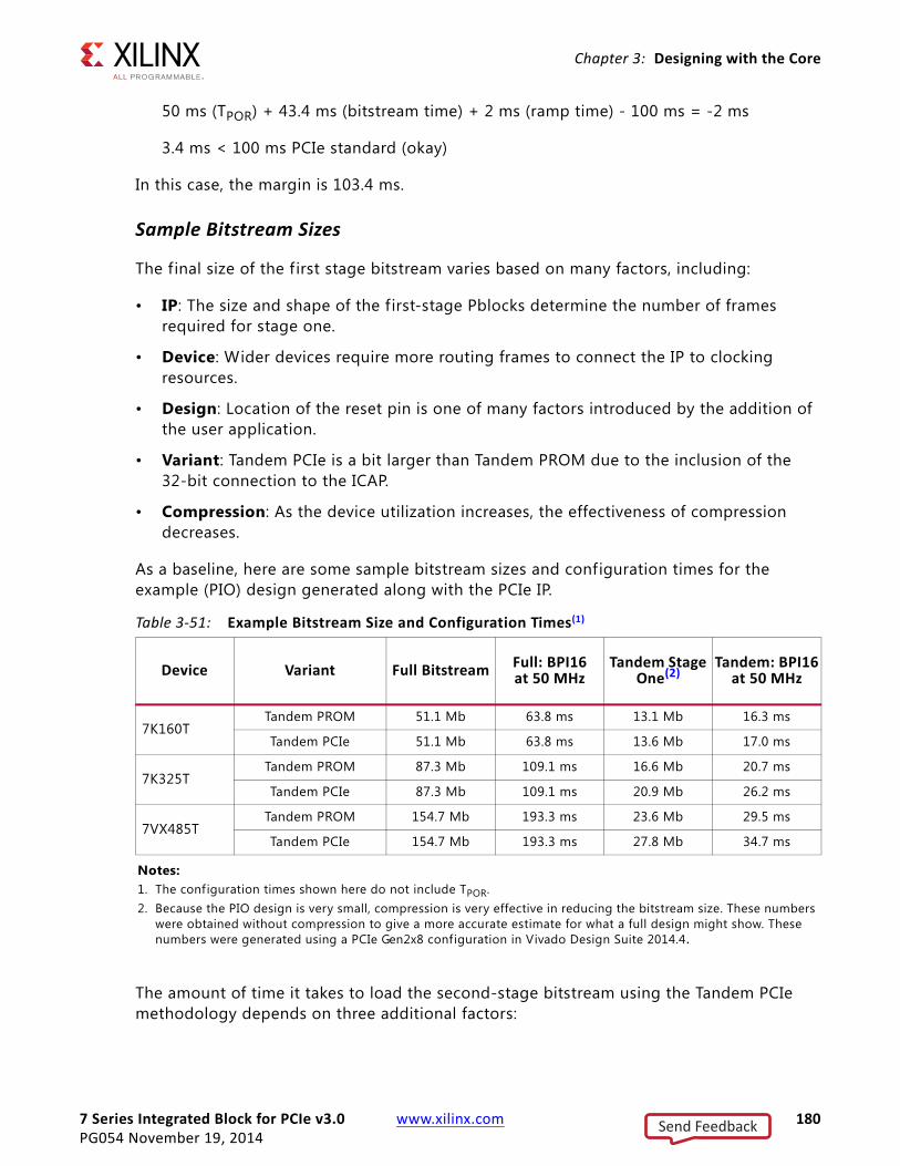
7 Series Integrated Block for PCIe v3.0 www.xilinx.com 180PG054 November 19, 2014
Chapter 3: Designing with the Core
50 ms (TPOR) + 43.4 ms (bitstream time) + 2 ms (ramp time) - 100 ms = -2 ms
3.4 ms < 100 ms PCIe standard (okay)
In this case, the margin is 103.4 ms.
Sample Bitstream Sizes
The final size of the f irst stage bitstream varies based on many factors, including:
• IP: The size and shape of the first-stage Pblocks determine the number of frames required for stage one.
• Device: Wider devices require more routing frames to connect the IP to clocking resources.
• Design: Location of the reset pin is one of many factors introduced by the addition of the user application.
• Variant: Tandem PCIe is a bit larger than Tandem PROM due to the inclusion of the 32-bit connection to the ICAP.
• Compression: As the device utilization increases, the effectiveness of compression decreases.
As a baseline, here are some sample bitstream sizes and configuration times for the example (PIO) design generated along with the PCIe IP.
The amount of time it takes to load the second-stage bitstream using the Tandem PCIe methodology depends on three additional factors:
Table 3-51: Example Bitstream Size and Configuration Times(1)
Device Variant Full Bitstream Full: BPI16 at 50 MHz
Tandem Stage One(2)
Tandem: BPI16at 50 MHz
7K160TTandem PROM 51.1 Mb 63.8 ms 13.1 Mb 16.3 ms
Tandem PCIe 51.1 Mb 63.8 ms 13.6 Mb 17.0 ms
7K325TTandem PROM 87.3 Mb 109.1 ms 16.6 Mb 20.7 ms
Tandem PCIe 87.3 Mb 109.1 ms 20.9 Mb 26.2 ms
7VX485TTandem PROM 154.7 Mb 193.3 ms 23.6 Mb 29.5 ms
Tandem PCIe 154.7 Mb 193.3 ms 27.8 Mb 34.7 ms
Notes: 1. The configuration times shown here do not include TPOR.2. Because the PIO design is very small, compression is very effective in reducing the bitstream size. These numbers
were obtained without compression to give a more accurate estimate for what a full design might show. These numbers were generated using a PCIe Gen2x8 configuration in Vivado Design Suite 2014.4.
Send Feedback
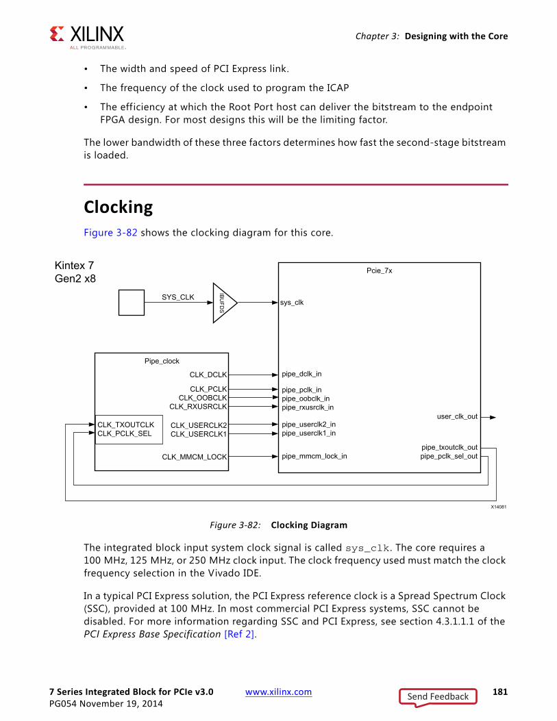
7 Series Integrated Block for PCIe v3.0 www.xilinx.com 181PG054 November 19, 2014
Chapter 3: Designing with the Core
• The width and speed of PCI Express link.
• The frequency of the clock used to program the ICAP
• The efficiency at which the Root Port host can deliver the bitstream to the endpoint FPGA design. For most designs this will be the limiting factor.
The lower bandwidth of these three factors determines how fast the second-stage bitstream is loaded.
ClockingFigure 3-82 shows the clocking diagram for this core.
The integrated block input system clock signal is called sys_clk . The core requires a 100 MHz, 125 MHz, or 250 MHz clock input. The clock frequency used must match the clock frequency selection in the Vivado IDE.
In a typical PCI Express solution, the PCI Express reference clock is a Spread Spectrum Clock (SSC), provided at 100 MHz. In most commercial PCI Express systems, SSC cannot be disabled. For more information regarding SSC and PCI Express, see section 4.3.1.1.1 of the PCI Express Base Specification [Ref 2].
X-Ref Target - Figure 3-82
Figure 3-82: Clocking Diagram
Send Feedback

7 Series Integrated Block for PCIe v3.0 www.xilinx.com 182PG054 November 19, 2014
Chapter 3: Designing with the Core
Synchronous and Non-Synchronous ClockingThere are two ways to clock the PCI Express system:
• Using synchronous clocking, where a shared clock source is used for all devices.
• Using non-synchronous clocking, where each device has its own clock source. ASPM must not be used in systems with non-synchronous clocking. When this mode is used, set the PCIE_ASYNC_EN to TRUE. For more details, AR 52400.
RECOMMENDED: Use synchronous clocking when using the core. All add-in card designs must use synchronous clocking due to the characteristics of the provided reference clock. For devices using the Slot clock, the Slot Clock Configuration setting in the Link Status Register must be enabled in the Vivado IDE. See the 7 Series FPGAs GTX Transceivers User Guide (UG476) and device data sheet for additional information regarding reference clock requirements.
For synchronous clocked systems, each link partner device shares the same clock source. Figure 3-83 and Figure 3-85 show a system using a 100 MHz reference clock. When using the 125 MHz or the 250 MHz reference clock option, an external PLL must be used to do a multiply of 5/4 and 5/2 to convert the 100 MHz clock to 125 MHz and 250 MHz, respectively, as illustrated in Figure 3-84 and Figure 3-86.
Further, even if the device is part of an embedded system, if the system uses commercial PCI Express root complexes or switches along with typical motherboard clocking schemes, synchronous clocking should still be used as shown in Figure 3-83 and Figure 3-84.
Figure 3-83 through Figure 3-86 illustrate high-level representations of the board layouts. You must ensure that proper coupling, and termination are used when laying out the board.
X-Ref Target - Figure 3-83
Figure 3-83: Embedded System Using 100 MHz Reference Clock
UG477_c5_67_092110
Embedded System Board
7 Series FPGAEndpoint
GTX
PCIe Link
PCIe LinkPCI Express
Switch or Root Complex
Device
PCI ExpressClock Oscillator
100 MHz
100 MHz
Send Feedback
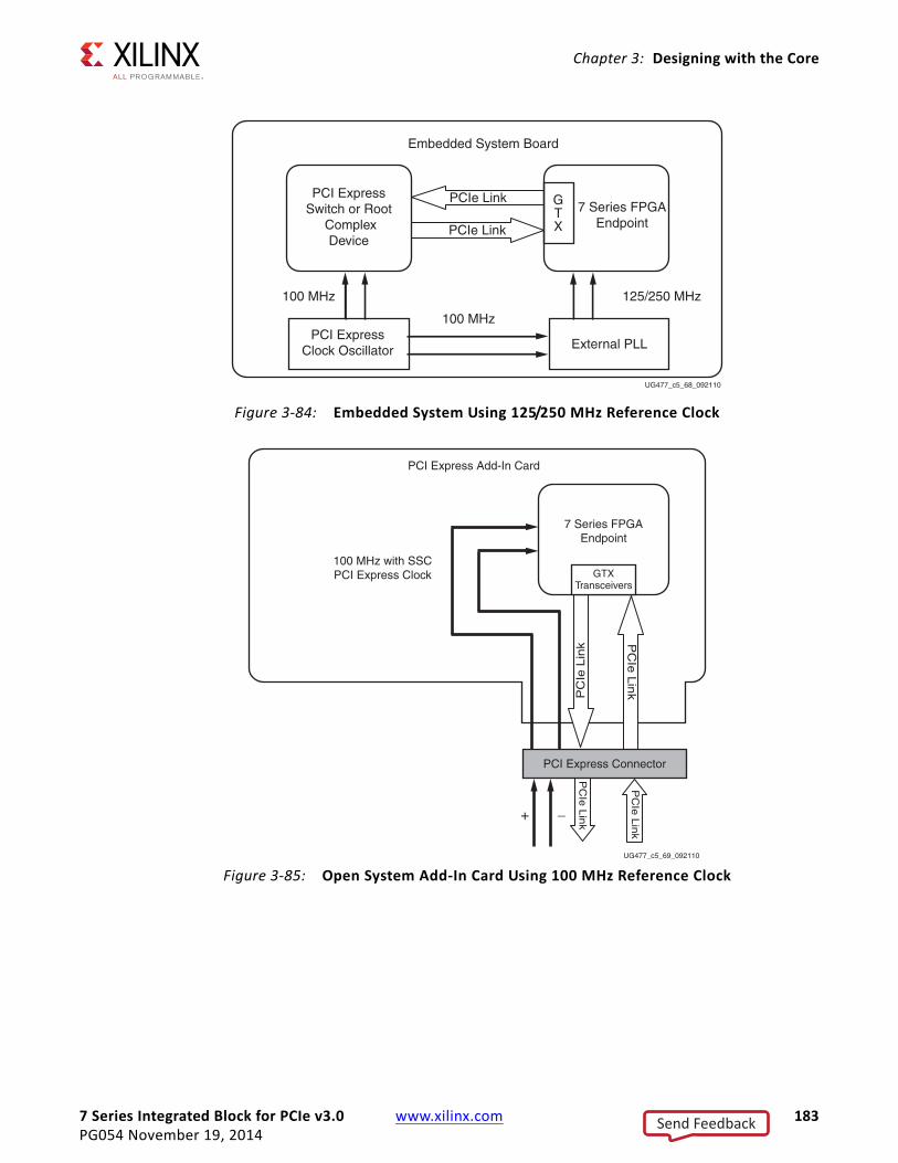
7 Series Integrated Block for PCIe v3.0 www.xilinx.com 183PG054 November 19, 2014
Chapter 3: Designing with the Core
X-Ref Target - Figure 3-84
Figure 3-84: Embedded System Using 125/250 MHz Reference ClockX-Ref Target - Figure 3-85
Figure 3-85: Open System Add-In Card Using 100 MHz Reference Clock
UG477_c5_68_092110
Embedded System Board
PCIe Link
PCIe LinkPCI Express
Switch or Root Complex
Device
PCI ExpressClock Oscillator External PLL
125/250 MHz
100 MHz
100 MHz
GTX
7 Series FPGAEndpoint
UG477_c5_69_092110
P
CIe
Lin
k PC
Ie L
ink
PC
Ie L
ink
PC
Ie L
ink
PCI Express Connector
7 Series FPGAEndpoint
GTXTransceivers
100 MHz with SSCPCI Express Clock
PCI Express Add-In Card
+ _
Send Feedback
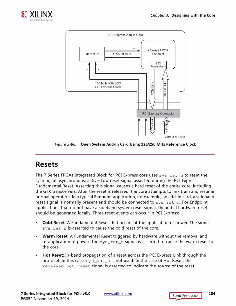
7 Series Integrated Block for PCIe v3.0 www.xilinx.com 184PG054 November 19, 2014
Chapter 3: Designing with the Core
ResetsThe 7 Series FPGAs Integrated Block for PCI Express core uses sys_rst_n to reset the system, an asynchronous, active-Low reset signal asserted during the PCI Express Fundamental Reset. Asserting this signal causes a hard reset of the entire core, including the GTX transceivers. After the reset is released, the core attempts to link train and resume normal operation. In a typical Endpoint application, for example, an add-in card, a sideband reset signal is normally present and should be connected to sys_rst_n. For Endpoint applications that do not have a sideband system reset signal, the initial hardware reset should be generated locally. Three reset events can occur in PCI Express:
• Cold Reset. A Fundamental Reset that occurs at the application of power. The signal sys_rst_n is asserted to cause the cold reset of the core.
• Warm Reset. A Fundamental Reset triggered by hardware without the removal and re-application of power. The sys_rst_n signal is asserted to cause the warm reset to the core.
• Hot Reset: In-band propagation of a reset across the PCI Express Link through the protocol. In this case, sys_rst_n is not used. In the case of Hot Reset, the received_hot_reset signal is asserted to indicate the source of the reset.
X-Ref Target - Figure 3-86
Figure 3-86: Open System Add-In Card Using 125/250 MHz Reference Clock
UG477_c5_70_092110
PC
Ie L
ink P
CIe Link
PCI Express Connector
7 Series FPGAEndpoint
GTXTransceivers
100 MHz with SSCPCI Express Clock
External PLL 125/250 MHz
PCI Express Add-In Card
+
-
+ -P
CIe
Lin
kPC
Ie L
ink
Send Feedback

7 Series Integrated Block for PCIe v3.0 www.xilinx.com 185PG054 November 19, 2014
Chapter 3: Designing with the Core
The user application interface of the core has an output signal called user_reset_out. This signal is deasserted synchronously with respect to user_clk_out. Signal user_reset_out is asserted as a result of any of these conditions:
• Fundamental Reset: Occurs (cold or warm) due to assertion of sys_rst_n.
• PLL within the Core Wrapper : Loses lock, indicating an issue with the stability of the clock input.
• Loss of Transceiver PLL Lock: Any transceiver loses lock, indicating an issue with the PCI Express Link.
The user_reset_out signal deasserts synchronously with user_clk_out after all of the above conditions are resolved, allowing the core to attempt to train and resume normal operation.
IMPORTANT: Systems designed to the PCI Express electro-mechanical specification provide a sideband reset signal, which uses 3.3V signaling levels—see the FPGA device data sheet to understand the requirements for interfacing to such signals.
Protocol LayersThe functions of the protocol layers, as defined by the PCI Express Base Specification [Ref 2], include generation and processing of Transaction Layer Packets (TLPs), flow control management, initialization, power management, data protection, error checking and retry, physical link interface initialization, maintenance and status tracking, serialization, deserialization, and other circuitry for interface operation. Each layer is defined in the next subsections.
Transaction LayerThe Transaction Layer is the upper layer of the PCI Express architecture, and its primary function is to accept, buffer, and disseminate Transaction Layer packets or TLPs. TLPs communicate information through the use of memory, I/O, configuration, and message transactions. To maximize the eff iciency of communication between devices, the Transaction Layer enforces PCI compliant Transaction ordering rules and manages TLP buffer space through credit-based flow control.
Data Link LayerThe Data Link Layer acts as an intermediate stage between the Transaction Layer and the Physical Layer. Its primary responsibility is to provide a reliable mechanism for the exchange of TLPs between two components on a link.
Send Feedback
7 Series Integrated Block for PCIe v3.0 www.xilinx.com 186PG054 November 19, 2014
Chapter 3: Designing with the Core
Services provided by the Data Link Layer include data exchange (TLPs), error detection and recovery, initialization services and the generation and consumption of Data Link Layer Packets (DLLPs). DLLPs are used to transfer information between Data Link Layers of two directly connected components on the link. DLLPs convey information such as Power Management, Flow Control, and TLP acknowledgments.
Physical LayerThe Physical Layer interfaces the Data Link Layer with signaling technology for link data interchange, and is subdivided into the Logical sub-block and the Electrical sub-block.
• The Logical sub-block frames and deframes TLPs and DLLPs. It also implements the Link Training and Status State machine (LTSSM), which handles link initialization, training, and maintenance. Scrambling, descrambling, and 8B/10B encoding and decoding of data is also performed in this sub-block.
• The Electrical sub-block defines the input and output buffer characteristics that interfaces the device to the PCIe® link.
The Physical Layer also supports Lane Reversal (for multi-lane designs) and Lane Polarity Inversion, as indicated in the PCI Express Base Specification, rev. 2.1 [Ref 2] requirement.
Configuration ManagementThe Configuration Management layer maintains the PCI™ Type 0 Endpoint configuration space and supports these features:
• Implements the PCI Configuration Space
• Supports Configuration Space accesses
• Power Management functions
• Implements error reporting and status functionality
• Implements packet processing functions
° Receive
- Configuration Reads and Writes
° Transmit
- Completions with or without data
- Transaction Layer Module (TLM) Error Messaging
- User Error Messaging
- Power Management Messaging/Handshake
• Implements MSI and INTx interrupt emulation
Send Feedback
7 Series Integrated Block for PCIe v3.0 www.xilinx.com 187PG054 November 19, 2014
Chapter 3: Designing with the Core
• Optionally implements MSIx Capability Structure in the PCI Configuration Space
• Optionally implements the Device Serial Number Capability in the PCI Express Extended Capability Space
• Optionally implements Virtual Channel Capability (support only for VC0) in the PCI Express Extended Capability Space
• Optionally implements Xilinx defined Vendor Specific Capability Structure in the PCI Express Extended Capability space to provide Loopback Control and Status
• Optionally implements Advanced Error Reporting (AER) Capability Structure in the PCI Express Extended Configuration Space
• Optionally implements Resizable BAR (RBAR) Capability Structure in the PCI Express Extended Configuration Space
Shared LogicThis new feature allows you to share common logic across multiple instances of PCIe Blocks or with other cores with certain limitations. The Shared Logic feature minimizes the HDL modif ications needed by bringing the logic to be shared to the top module of the design; it also enables additional ports on the top module to enable sharing. This feature is applicable only for the Endpoint mode, and not the Root Port mode.
In the Vivado Design Suite, the shared logic options are available in the Shared Logic page when customizing the core.
There are four types of logic sharing:
• Shared Clocking
• Shared GT_COMMON
• Shared GT_COMMON and Clocking
• Internal Shared GT_COMMON and Clocking
IMPORTANT: For Shared Clocking option Include Shared Logic (Clocking) in example design (default mode), Shared GT_COMMON option Include Shared Logic (Transceiver GT_COMMON) in example design, and Shared GT_COMMON and Clocking, to generate the corresponding modules in the support directory, you must run the Open IP Example Design command after the output products are generated. For the option Include Shared Logic in Core, these modules are generated in the source directory.
Shared ClockingTo use the share clocking feature, select Include Shared Logic (Clocking) in example design option in the in the Shared Logic tab (Figure 3-87).
Send Feedback
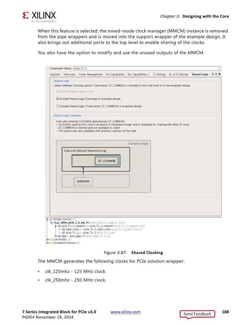
7 Series Integrated Block for PCIe v3.0 www.xilinx.com 188PG054 November 19, 2014
Chapter 3: Designing with the Core
When this feature is selected, the mixed-mode clock manager (MMCM) instance is removed from the pipe wrappers and is moved into the support wrapper of the example design. It also brings out additional ports to the top level to enable sharing of the clocks.
You also have the option to modify and use the unused outputs of the MMCM.
The MMCM generates the following clocks for PCIe solution wrapper:
• clk_125mhz - 125 MHz clock.
• clk_250mhz - 250 MHz clock.
X-Ref Target - Figure 3-87
Figure 3-87: Shared Clocking
Send Feedback

7 Series Integrated Block for PCIe v3.0 www.xilinx.com 189PG054 November 19, 2014
Chapter 3: Designing with the Core
• userclk - 62.5 MHz / 125 MHz / 250 MHz clock, depending on selected PCIe core lane width, link speed, and AXI interface width.
• userclk2 – 250 MHz / 500 MHz clock, depending on selected PCIe core link speed.
• oobclk
The other cores/logic present in the user design can use any of the MMCM outputs listed above.
The MMCM instantiated in the PCIe example design has two unconnected outputs: CLKOUT5, and CLKOUT6. These outputs can be used to generate other desired clock frequencies by selecting the appropriate CLKOUT5_DIVIDE and CLKOUT6_DIVIDE parameters for MMCM.
TIP: Sharing the MMCM between PCIe and other cores in your design saves FPGA resources and eases output clock path routing.
Limitations
• Reference clock input to MMCM is restricted to 100 MHz in most use cases.
° There is an option for selecting a reference clock of 125MHz or 250MHz, which is not a common use case.
• The MMCM reset is tied to a static value in the top module. The MMCM can be reset as required by the system design. The MMCM reset can be asserted only after reference clock is recovered and is stable. Also, MMCM reset is indirectly tied to the PCIe core reset and asserting MMCM reset resets the PCIe core.
• Userclk1 and Userclk2 outputs are selected based on the PCIe Lane Width, Link Speed, and AXI width selections (for details, see Chapter 4, Customizing and Generating the Core). Sharing cores must comply with these requirements.
Shared GT_COMMONA quad phase-locked loop (QPLL) in GT_COMMON can serve a quad of GT_CHANNEL instances. If the PCIe core is configured as X1 or X2 and is using a QPLL, the remaining GT_CHANNEL instances can be used by other cores by sharing the same QPLL and GT_COMMON.
To use the shared GT_COMMON instances, select the Include Shared Logic (Transceiver GT_COMMON) in example design option in the Shared Logic tab (Figure 3-88).
When this feature is selected, the GT_COMMON instance is removed from the pipe wrappers and is moved into the support wrapper of the example design. It also brings out additional ports to the top level to enable sharing of the GT_COMMON.
Send Feedback
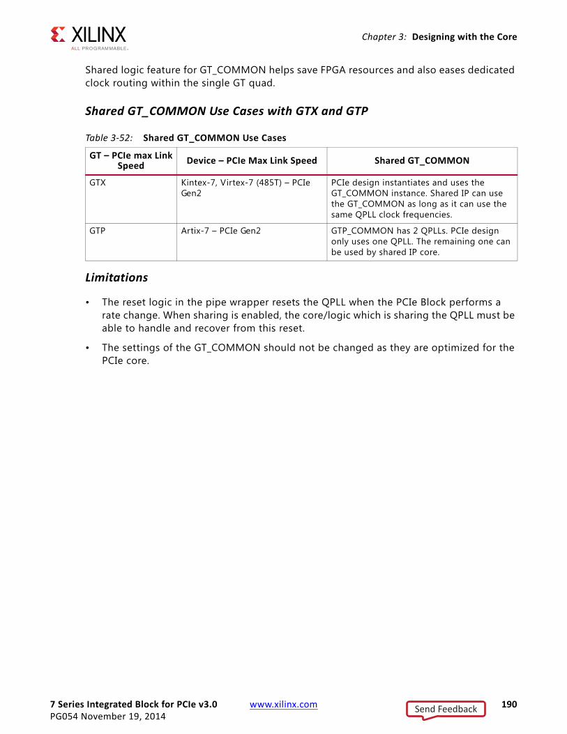
7 Series Integrated Block for PCIe v3.0 www.xilinx.com 190PG054 November 19, 2014
Chapter 3: Designing with the Core
Shared logic feature for GT_COMMON helps save FPGA resources and also eases dedicated clock routing within the single GT quad.
Shared GT_COMMON Use Cases with GTX and GTP
Limitations
• The reset logic in the pipe wrapper resets the QPLL when the PCIe Block performs a rate change. When sharing is enabled, the core/logic which is sharing the QPLL must be able to handle and recover from this reset.
• The settings of the GT_COMMON should not be changed as they are optimized for the PCIe core.
Table 3-52: Shared GT_COMMON Use Cases
GT – PCIe max Link Speed Device – PCIe Max Link Speed Shared GT_COMMON
GTX Kintex-7, Virtex-7 (485T) – PCIe Gen2
PCIe design instantiates and uses the GT_COMMON instance. Shared IP can use the GT_COMMON as long as it can use the same QPLL clock frequencies.
GTP Artix-7 – PCIe Gen2 GTP_COMMON has 2 QPLLs. PCIe design only uses one QPLL. The remaining one can be used by shared IP core.
Send Feedback
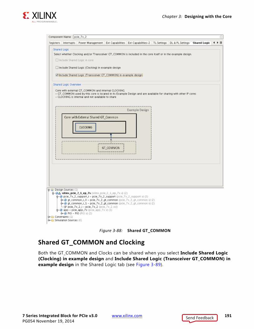
7 Series Integrated Block for PCIe v3.0 www.xilinx.com 191PG054 November 19, 2014
Chapter 3: Designing with the Core
Shared GT_COMMON and ClockingBoth the GT_COMMON and Clocks can be shared when you select Include Shared Logic (Clocking) in example design and Include Shared Logic (Transceiver GT_COMMON) in example design in the Shared Logic tab (see Figure 3-89).
X-Ref Target - Figure 3-88
Figure 3-88: Shared GT_COMMON
Send Feedback
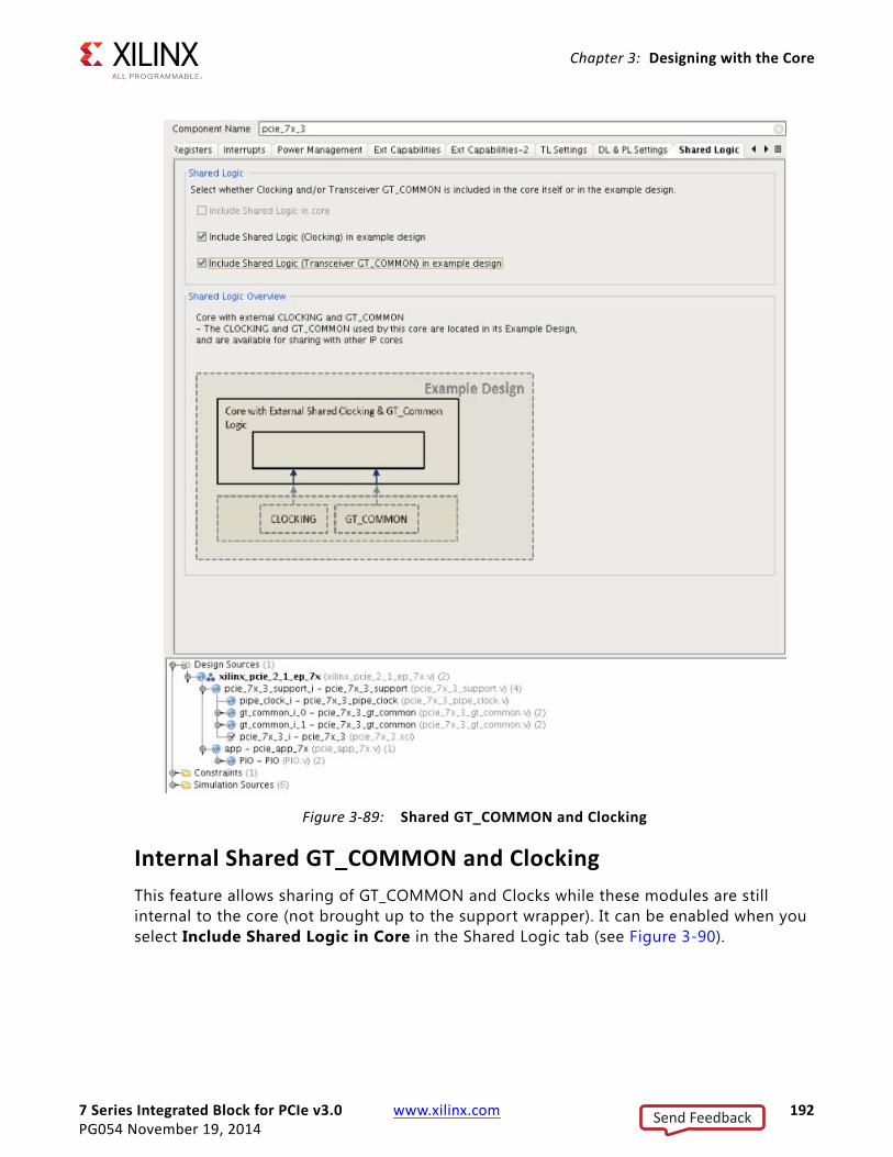
7 Series Integrated Block for PCIe v3.0 www.xilinx.com 192PG054 November 19, 2014
Chapter 3: Designing with the Core
Internal Shared GT_COMMON and ClockingThis feature allows sharing of GT_COMMON and Clocks while these modules are still internal to the core (not brought up to the support wrapper). It can be enabled when you select Include Shared Logic in Core in the Shared Logic tab (see Figure 3-90).
X-Ref Target - Figure 3-89
Figure 3-89: Shared GT_COMMON and Clocking
Send Feedback
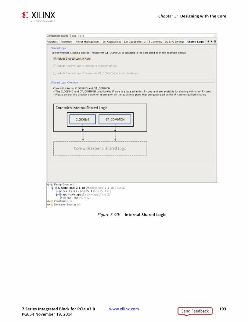
7 Series Integrated Block for PCIe v3.0 www.xilinx.com 193PG054 November 19, 2014
Chapter 3: Designing with the Core
X-Ref Target - Figure 3-90
Figure 3-90: Internal Shared Logic
Send Feedback

7 Series Integrated Block for PCIe v3.0 www.xilinx.com 194PG054 November 19, 2014
Chapter 3: Designing with the Core
Clocking InterfaceTable 3-53 defines the clocking interface signals.
The Clocking architecture is described in detail in the Use Model chapter of the 7 Series FPGAs GTX/GTH Transceivers User Guide (UG476) [Ref 12].
FPGA ConfigurationThis section discusses how to configure the 7 series FPGA so that the device can link up and be recognized by the system. This information is provided for you to choose the correct FPGA configuration method for the system and verify that it works as expected.
This section discusses how specif ic requirements of the PCI Express Base Specification and PCI Express Card Electromechanical Specification [Ref 2] apply to FPGA configuration.
RECOMMENDED: Where appropriate, Xilinx recommends that you read the actual specifications for detailed information.
Table 3-53: Clocking Interface Signals
Name Direction Description
pipe_pclk_in Input Parallel clock used to synchronize data transfers across the parallel interface of the GTX transceiver.
pipe_rxusrclk_in Input Provides a clock for the internal RX PCS datapath.
pipe_rxoutclk_in Input Recommended clock output to the FPGA logic.
pipe_dclk_in Input Dynamic reconfiguration clock.
pipe_userclk1_in Input Optional user clock.
pipe_userclk2_in Input Optional user clock.
pipe_mmcm_lock_in Input Indicates if the MMCM is locked onto the source CLK.
pipe_txoutclk_out Output Recommended clock output to the FPGA logic.
pipe_rxoutclk_out Output Recommended clock output to the FPGA logic.
pipe_pclk_sel_out Output Parallel clock select.
pipe_gen3_out Output Indicates the PCI Express operating speed.
pipe_mmcm_rst_n MMCM reset port. This port could be used by the upper layer to reset MMCM if error recovery is required. If the system detects the deassertion of MMCM lock, Xilinx recommends that you reset the MMCM. The recommended approach is to reset the MMCM after the MMCM input clock recovers (if MMCM reset occurs before the input reference clock recovers, the MMCM might never relock). After MMCM is reset, wait for MMCM to lock and then reset the PIPE Wrapper as normally done. Currently this port is tied High.
Send Feedback
7 Series Integrated Block for PCIe v3.0 www.xilinx.com 195PG054 November 19, 2014
Chapter 3: Designing with the Core
See Tandem PROM, page 155 for more information on meeting configuration requirements after reading this section.
This section contains these subsections:
• Configuration Terminology. Defines terms used in this section.
• Configuration Access Time. Several specification items govern when an Endpoint device needs to be ready to receive configuration accesses from the host (Root Complex).
• Board Power in Real-World Systems. Understanding real-world system constraints related to board power and how they affect the specification requirements.
• Recommendations. Describes methods for FPGA configuration and includes sample issue analysis for FPGA configuration timing issues.
Configuration TerminologyIn this section, these terms are used to differentiate between FPGA configuration and configuration of the PCI Express® device:
• Configuration of the FPGA. FPGA configuration is used.
• Configuration of the PCI Express device. After the link is active, configuration is used.
Configuration Access TimeIn standard systems for PCI Express, when the system is powered up, configuration software running on the processor starts scanning the PCI Express bus to discover the machine topology.
The process of scanning the PCI Express hierarchy to determine its topology is referred to as the enumeration process. The root complex accomplishes this by initiating configuration transactions to devices as it traverses and determines the topology.
All PCI Express devices are expected to have established the link with their link partner and be ready to accept configuration requests during the enumeration process. As a result, there are requirements as to when a device needs to be ready to accept configuration requests after powerup; if the requirements are not met, this occurs:
• If a device is not ready and does not respond to configuration requests, the root complex does not discover it and treats it as non-existent.
• The operating system does not report the existence of the device, and the user application is not able to communicate with the device.
Choosing the appropriate FPGA configuration method is key to ensuring the device is able to communicate with the system in time to achieve link up and respond to the configuration accesses.
Send Feedback

7 Series Integrated Block for PCIe v3.0 www.xilinx.com 196PG054 November 19, 2014
Chapter 3: Designing with the Core
Configuration Access Specification Requirements
Two PCI Express specification items are relevant to configuration access:
1. Section 6.6 of PCI Express Base Specification, rev 1.1 states “A system must guarantee that all components intended to be software visible at boot time are ready to receive Configuration Requests within 100 ms of the end of Fundamental Reset at the Root Complex.” For detailed information about how this is accomplished, see the specification [Ref 2].
Xilinx compliance to this specif ication is validated by the PCI Express-CV tests. The PCI Special Interest Group (PCI-SIG) provides the PCI Express Configuration Test Software to verify the device meets the requirement of being able to receive configuration accesses within 100 ms of the end of the fundamental reset. The software, available to any member of the PCI-SIG, generates several resets using the in-band reset mechanism and PERST# toggling to validate robustness and compliance to the specif ication.
2. Section 6.6 of PCI Express Base Specification v1.1 [Ref 2] defines three parameters necessary “where power and PERST# are supplied.” The parameter TPVPERL applies to FPGA configuration timing and is defined as:
TPVPERL - PERST# must remain active at least this long after power becomes valid.
The PCI Express Base Specification does not give a specif ic value for TPVPERL – only its meaning is defined. The most common form factor used with the core is an ATX-based form factor. The PCI Express Card Electromechanical Specification [Ref 2] focuses on requirements for ATX-based form factors. This applies to most designs targeted to standard desktop or server type motherboards. Figure 3-91 shows the relationship between Power Stable and PERST#.
Section 2.6.2 of the PCI Express Card Electromechanical Specification, v1.1 [Ref 2] defines TPVPREL as a minimum of 100 ms, indicating that from the time power is stable the system
X-Ref Target - Figure 3-91
Figure 3-91: Power Up
3.3 VAUX
3.3V/12V
PERST#
PCI Express Link Inactive Active
Power Stable
100 ms
TPVPERL
Send Feedback

7 Series Integrated Block for PCIe v3.0 www.xilinx.com 197PG054 November 19, 2014
Chapter 3: Designing with the Core
reset is asserted for at least 100 ms (as shown in Table 3-54).
From Figure 3-91 and Table 3-54, it is possible to obtain a simple equation to define the FPGA configuration time as follows:
FPGA Configuration Time ≤ TPWRVLD + TPVPERL Equation 3-1
Given that TPVPERL is defined as 100 ms minimum, this becomes:
FPGA Configuration Time ≤ TPWRVLD + 100 ms Equation 3-2
Note: Although TPWRVLD is included in Equation 3-2, it has yet to be defined in this discussion because it depends on the type of system in use. The Board Power in Real-World Systems section defines TPWRVLD for both ATX-based and non ATX-based systems.
FPGA configuration time is only relevant at cold boot; subsequent warm or hot resets do not cause reconfiguration of the FPGA. If the design appears to be having issues due to FPGA configuration, you should issue a warm reset as a simple test, which resets the system, including the PCI Express link, but keeps the board powered. If the issue does not appear, the issue could be FPGA configuration time related.
Table 3-54: TPVPERL Specification
Symbol Parameter Min Max Units
TPVPERL Power stable to PERST# inactive
100 ms
Send Feedback
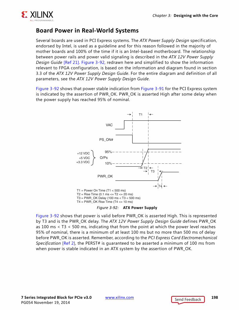
7 Series Integrated Block for PCIe v3.0 www.xilinx.com 198PG054 November 19, 2014
Chapter 3: Designing with the Core
Board Power in Real-World SystemsSeveral boards are used in PCI Express systems. The ATX Power Supply Design specification, endorsed by Intel, is used as a guideline and for this reason followed in the majority of mother boards and 100% of the time if it is an Intel-based motherboard. The relationship between power rails and power valid signaling is described in the ATX 12V Power Supply Design Guide [Ref 21]. Figure 3-92, redrawn here and simplif ied to show the information relevant to FPGA configuration, is based on the information and diagram found in section 3.3 of the ATX 12V Power Supply Design Guide. For the entire diagram and definition of all parameters, see the ATX 12V Power Supply Design Guide.
Figure 3-92 shows that power stable indication from Figure 3-91 for the PCI Express system is indicated by the assertion of PWR_OK. PWR_OK is asserted High after some delay when the power supply has reached 95% of nominal.
Figure 3-92 shows that power is valid before PWR_OK is asserted High. This is represented by T3 and is the PWR_OK delay. The ATX 12V Power Supply Design Guide defines PWR_OK as 100 ms < T3 < 500 ms, indicating that from the point at which the power level reaches 95% of nominal, there is a minimum of at least 100 ms but no more than 500 ms of delay before PWR_OK is asserted. Remember, according to the PCI Express Card Electromechanical Specification [Ref 2], the PERST# is guaranteed to be asserted a minimum of 100 ms from when power is stable indicated in an ATX system by the assertion of PWR_OK.
X-Ref Target - Figure 3-92
Figure 3-92: ATX Power Supply
VAC
PS_ON#
O/Ps
PWR_OK
+12 VDC
+5 VDC+3.3 VDC
T1
T2T3
T4T1 = Power On Time (T1 < 500 ms)T2 = Rise Time (0.1 ms <= T2 <= 20 ms)T3 = PWR_OK Delay (100 ms < T3 < 500 ms)T4 = PWR_OK Rise Time (T4 <= 10 ms)
95%
10%
Send Feedback
7 Series Integrated Block for PCIe v3.0 www.xilinx.com 199PG054 November 19, 2014
Chapter 3: Designing with the Core
Again, the FPGA configuration time equation is:
FPGA Configuration Time ≤ TPWRVLD + 100 ms Equation 3-3
TPWRVLD is defined as PWR_OK delay period; that is, TPWRVLD represents the amount of time that power is valid in the system before PWR_OK is asserted. This time can be added to the amount of time the FPGA has to configure. The minimum values of T2 and T4 are negligible and considered zero for purposes of these calculations. For ATX-based motherboards, which represent the majority of real-world motherboards in use, TPWRVLD can be defined as:
100 ms ≤ TPWRVLD ≤ 500 ms Equation 3-4
This provides these requirements for FPGA configuration time in both ATX and non-ATX-based motherboards:
• FPGA Configuration Time ≤ 200 ms (for ATX based motherboard)
• FPGA Configuration Time ≤ 100 ms (for non-ATX based motherboard)
The second equation for the non-ATX based motherboards assumes a TPWRVLD value of 0 ms because it is not defined in this context. Designers with non-ATX based motherboards should evaluate their own power supply design to obtain a value for TPWRVLD.
This section assumes that the FPGA power (VCCINT) is stable before or at the same time that PWR_OK is asserted. If this is not the case, then additional time must be subtracted from the available time for FPGA configuration.
IMPORTANT: Avoid designing add-in cards with staggered voltage regulators with long delays.
Hot Plug Systems
Hot Plug systems generally employ the use of a Hot-Plug Power Controller located on the system motherboard. Many discrete Hot-Plug Power Controllers extend TPVPERL beyond the minimum 100 ms. Add-in card designers should consult the Hot-Plug Power Controller data sheet to determine the value of TPVPERL. If the Hot-Plug Power Controller is unknown, then a TPVPERL value of 100 ms should be assumed.
RecommendationsRECOMMENDED: For minimum FPGA configuration time, Xilinx recommends the BPI configuration mode with a parallel NOR flash, which supports high-speed synchronous read operation.
In addition, an external clock source can be supplied to the external master configuration clock (EMCCLK) pin to ensure a consistent configuration clock frequency for all conditions. See 7 Series FPGAs Configuration User Guide (UG470) [Ref 7] for descriptions of the BPI configuration mode and EMCCLK pin. This section discusses these recommendations and includes sample analysis of potential issues that might arise during FPGA configuration.
Send Feedback
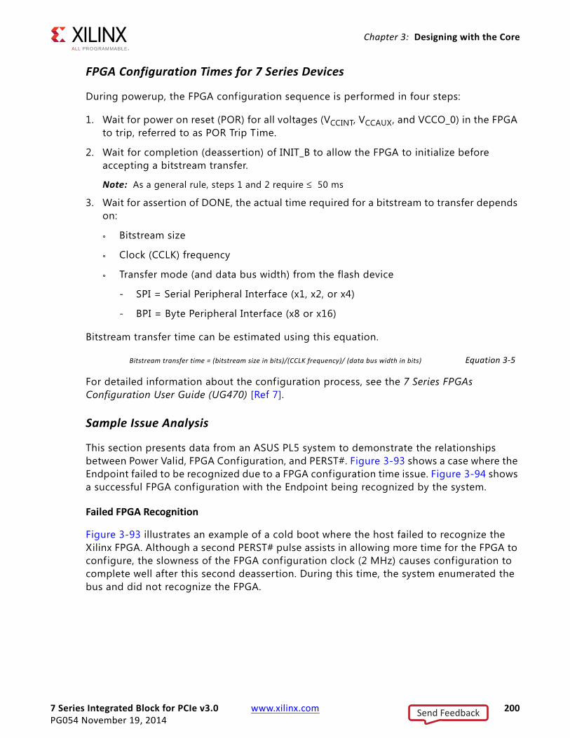
7 Series Integrated Block for PCIe v3.0 www.xilinx.com 200PG054 November 19, 2014
Chapter 3: Designing with the Core
FPGA Configuration Times for 7 Series Devices
During powerup, the FPGA configuration sequence is performed in four steps:
1. Wait for power on reset (POR) for all voltages (VCCINT, VCCAUX, and VCCO_0) in the FPGA to trip, referred to as POR Trip Time.
2. Wait for completion (deassertion) of INIT_B to allow the FPGA to initialize before accepting a bitstream transfer.
Note: As a general rule, steps 1 and 2 require ≤ 50 ms
3. Wait for assertion of DONE, the actual time required for a bitstream to transfer depends on:
° Bitstream size
° Clock (CCLK) frequency
° Transfer mode (and data bus width) from the flash device
- SPI = Serial Peripheral Interface (x1, x2, or x4)
- BPI = Byte Peripheral Interface (x8 or x16)
Bitstream transfer time can be estimated using this equation.
Bitstream transfer time = (bitstream size in bits)/(CCLK frequency)/ (data bus width in bits) Equation 3-5
For detailed information about the configuration process, see the 7 Series FPGAs Configuration User Guide (UG470) [Ref 7].
Sample Issue Analysis
This section presents data from an ASUS PL5 system to demonstrate the relationships between Power Valid, FPGA Configuration, and PERST#. Figure 3-93 shows a case where the Endpoint failed to be recognized due to a FPGA configuration time issue. Figure 3-94 shows a successful FPGA configuration with the Endpoint being recognized by the system.
Failed FPGA Recognition
Figure 3-93 illustrates an example of a cold boot where the host failed to recognize the Xilinx FPGA. Although a second PERST# pulse assists in allowing more time for the FPGA to configure, the slowness of the FPGA configuration clock (2 MHz) causes configuration to complete well after this second deassertion. During this time, the system enumerated the bus and did not recognize the FPGA.
Send Feedback
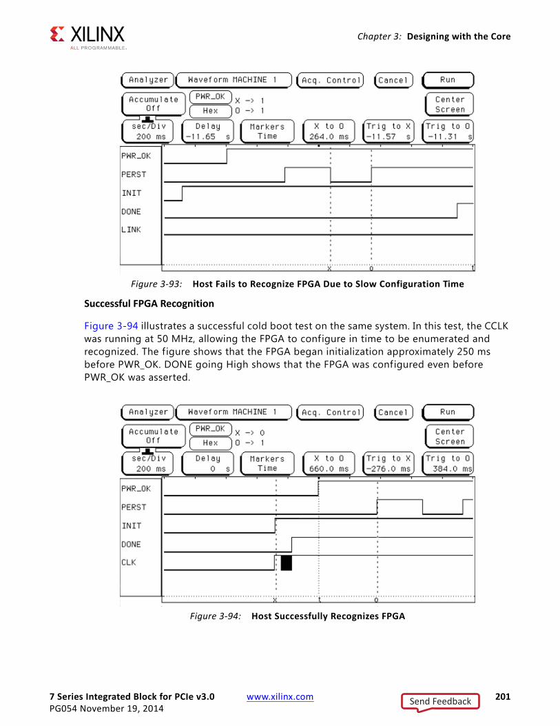
7 Series Integrated Block for PCIe v3.0 www.xilinx.com 201PG054 November 19, 2014
Chapter 3: Designing with the Core
Successful FPGA Recognition
Figure 3-94 illustrates a successful cold boot test on the same system. In this test, the CCLK was running at 50 MHz, allowing the FPGA to configure in time to be enumerated and recognized. The figure shows that the FPGA began initialization approximately 250 ms before PWR_OK. DONE going High shows that the FPGA was configured even before PWR_OK was asserted.
X-Ref Target - Figure 3-93
Figure 3-93: Host Fails to Recognize FPGA Due to Slow Configuration Time
X-Ref Target - Figure 3-94
Figure 3-94: Host Successfully Recognizes FPGA
Send Feedback

7 Series Integrated Block for PCIe v3.0 www.xilinx.com 202PG054 November 19, 2014
Chapter 3: Designing with the Core
Workarounds for Closed Systems
For failing FPGA configuration combinations, designers might be able to work around the issue in closed systems or systems where they can guarantee behavior. These options are not recommended for products where the targeted end system is unknown.
1. Check if the motherboard and BIOS generate multiple PERST# pulses at start-up. This can be determined by capturing the signal on the board using an oscilloscope. This is similar to what is shown in Figure 3-93. If multiple PERST# pulses are generated, this typically adds extra time for FPGA configuration.
Define TPERSTPERIOD as the total sum of the pulse width of PERST# and deassertion period before the next PERST# pulse arrives. Because the FPGA is not power cycled or reconfigured with additional PERST# assertions, the TPERSTPERIOD number can be added to the FPGA configuration equation.
FPGA Configuration Time ≤ TPWRVLD + TPERSTPERIOD + 100 ms Equation 3-6
2. In closed systems, it might be possible to create scripts to force the system to perform a warm reset after the FPGA is configured, after the initial powerup sequence. This resets the system along with the PCI Express subsystem allowing the device to be recognized by the system.
Send Feedback

7 Series Integrated Block for PCIe v3.0 www.xilinx.com 203PG054 November 19, 2014
Chapter 4
Design Flow StepsThis chapter describes customizing and generating the core, constraining the core, and the simulation, synthesis and implementation steps that are specific to this IP core. More detailed information about the standard Vivado® design flows in the Vivado IP Integrator can be found in the following Xilinx® Vivado Design Suite user guides:
• Vivado Design Suite User Guide: Designing IP Subsystems using IP Integrator (UG994) [Ref 18]
• Vivado Design Suite User Guide: Designing with IP (UG896) [Ref 14]
• Vivado Design Suite User Guide: Getting Started (UG910) [Ref 13]
• Vivado Design Suite User Guide: Logic Simulation (UG900) [Ref 15]
Customizing and Generating the CoreThis section includes information on using the Vivado Design Suite to customize and generate the core.
Note: If you are customizing and generating the core in the IP Integrator, see the Vivado Design Suite User Guide: Designing IP Subsystems using IP Integrator (UG994) [Ref 18] for detailed information. IP Integrator might auto-compute certain configuration values when validating or generating the design. To check whether the values do change, see the description of the parameter in this section. To view the parameter value you can run the validate_bd_design command in the Tcl Console.
The 7 Series FPGAs Integrated Block for PCI Express® core is a fully configurable and highly customizable solution. In the Vivado Integrated Design Environment (IDE), you can customize the IP for use in your design by specifying values for the various parameters associated with the IP core using the following steps:
1. Select the IP from the IP catalog.
2. Double-click the selected IP, or select the Customize IP command from the toolbar or right-click menu.
The Customize IP dialog box for the 7 Series FPGAs Integrated Block for PCI Express consists of two modes: Base Mode and Advanced Mode. To select a mode, use the Mode drop-down list on the first page of the Customize IP dialog box.
Send Feedback

7 Series Integrated Block for PCIe v3.0 www.xilinx.com 204PG054 November 19, 2014
Chapter 4: Design Flow Steps
For details, see the Vivado Design Suite User Guide: Designing with IP (UG896) [Ref 14], and the Vivado Design Suite User Guide: Getting Started (UG910) [Ref 13].
Note: Figures in this chapter are illustrations of the Vivado IDE. This layout might vary from the current version.
Base ModeThe Base mode parameters are explained in this section.
Basic
The initial customization page shown in Figure 4-1 is used to define the basic parameters for the core, including the component name, lane width, and link speed.
Component Name
Base name of the output f iles generated for the core. The name must begin with a letter and can be composed of these characters: a to z, 0 to 9, and “_.”
Mode
Allows to select the Basic or Advanced mode of the configuration of the core.
X-Ref Target - Figure 4-1
Figure 4-1: Basic Parameters
Send Feedback
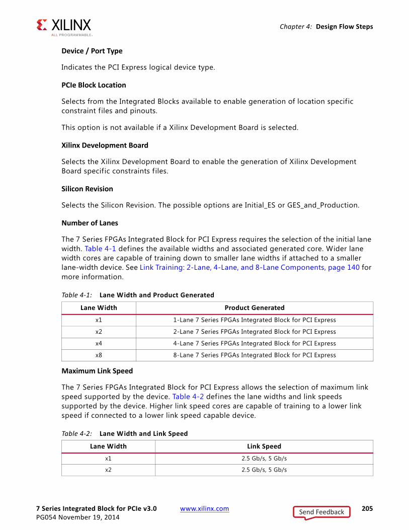
7 Series Integrated Block for PCIe v3.0 www.xilinx.com 205PG054 November 19, 2014
Chapter 4: Design Flow Steps
Device / Port Type
Indicates the PCI Express logical device type.
PCIe Block Location
Selects from the Integrated Blocks available to enable generation of location specific constraint f iles and pinouts.
This option is not available if a Xilinx Development Board is selected.
Xilinx Development Board
Selects the Xilinx Development Board to enable the generation of Xilinx Development Board specif ic constraints f iles.
Silicon Revision
Selects the Silicon Revision. The possible options are Initial_ES or GES_and_Production.
Number of Lanes
The 7 Series FPGAs Integrated Block for PCI Express requires the selection of the initial lane width. Table 4-1 defines the available widths and associated generated core. Wider lane width cores are capable of training down to smaller lane widths if attached to a smaller lane-width device. See Link Training: 2-Lane, 4-Lane, and 8-Lane Components, page 140 for more information.
Maximum Link Speed
The 7 Series FPGAs Integrated Block for PCI Express allows the selection of maximum link speed supported by the device. Table 4-2 defines the lane widths and link speeds supported by the device. Higher link speed cores are capable of training to a lower link speed if connected to a lower link speed capable device.
Table 4-1: Lane Width and Product Generated
Lane Width Product Generated
x1 1-Lane 7 Series FPGAs Integrated Block for PCI Express
x2 2-Lane 7 Series FPGAs Integrated Block for PCI Express
x4 4-Lane 7 Series FPGAs Integrated Block for PCI Express
x8 8-Lane 7 Series FPGAs Integrated Block for PCI Express
Table 4-2: Lane Width and Link Speed
Lane Width Link Speed
x1 2.5 Gb/s, 5 Gb/s
x2 2.5 Gb/s, 5 Gb/s
Send Feedback

7 Series Integrated Block for PCIe v3.0 www.xilinx.com 206PG054 November 19, 2014
Chapter 4: Design Flow Steps
AXI Interface Frequency
It is possible to select the clock frequency of the core user interface. Each lane width provides multiple frequency choices: a default frequency, and alternative frequencies, as defined in Table 4-3.
RECOMMENDED: Where possible, use the default frequency.
Selecting the alternate frequencies does not result in a difference in throughput in the core, but does allow the user application to run at an alternate speed.
AXI Interface Width
The 7 Series FPGAs Integrated Block for PCI Express allows the selection of interface width, as defined in Table 4-4. The default interface width is the lowest possible interface width.
x4 2.5 Gb/s, 5 Gb/s
x8 2.5 Gb/s, 5 Gb/s
Table 4-2: Lane Width and Link Speed
Lane Width Link Speed
Table 4-3: Recommended and Optional Transaction Clock (user_clk_out) Frequencies
Product Link Speed (Gb/s)
Interface Width(1) (Bits)
Recommended Frequency (MHz)
Optional Frequency (MHz)
1-lane 2.5 64 62.5 125, 250
1-lane 5 64 62.5 125, 250
2-lane 2.5 64 62.5 125, 250
2-lane 5 64 125 250
4-lane 2.5 64 125 250
4-lane 5 64 250 -
4-lane 5 128 125 -
8-lane 2.5 64 250 -
8-lane 2.5 128 125 -
8-lane 5 128 250 -
Notes: 1. Interface width is a static selection and does not change with dynamic link speed changes
Table 4-4: Lane Width, Link Speed, and Interface Width
Lane Width Link Speed(Gb/s) Interface Width (Bits)
X1 2.5, 5.0 64
X2 2.5, 5.0 64
Send Feedback
7 Series Integrated Block for PCIe v3.0 www.xilinx.com 207PG054 November 19, 2014
Chapter 4: Design Flow Steps
Reference Clock Frequency
Selects the frequency of the reference clock provided on sys_clk. For information about clocking the core, see Clocking and Resets in Chapter 3.
Tandem Configuration
The radio buttons, None, Tandem PROM and Tandem PCIe, allow you to choose the Tandem Configuration. The devices supported are K325T, K410T, K420T, V485T, and K160T. For Zynq 7Z030, 7Z045 and 7Z100 devices, only the Tandem PROM option is available. They do not support Tandem PCIe mode.
PIPE Mode Simulations
This group box provides two radio buttons to select either of two PIPE mode simulation mechanisms. This option is enabled for both Endpoint and Root Port configurations only when the Shared Logic (clocking) in example design option is selected (see Shared Logic, page 231).
• None: No PIPE mode simulation is available. This is the default value.
• Enable Pipe Simulation: When selected, this option generates the core that can be simulated with PIPE interfaces connected.
• Enable External PIPE Interface: This is for third-party PIPE simulation support. When selected, this option enables an external third-party bus functional model (BFM) to connect to the PIPE interface of PCIe block. For more information, see PIPE Mode Simulations, page 255.
Enable External GT Channel DRP
The external GT channel DRP ports are pulled out to the core top.
• ext_ch_gt_drpdo[15:0]
• ext_ch_gt_drpdi[15:0]
• ext_ch_gt_drpen[0:0]
• ext_ch_gt_drwe[0:0]
• ext_ch_gt_drprdy[:0]
X4 2.5 64
X4 5.0 64, 128
X8 2.5 64, 128
X8 5.0 128
Table 4-4: Lane Width, Link Speed, and Interface Width
Lane Width Link Speed(Gb/s) Interface Width (Bits)
Send Feedback
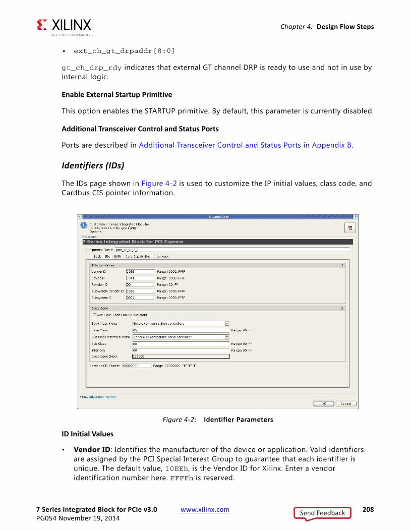
7 Series Integrated Block for PCIe v3.0 www.xilinx.com 208PG054 November 19, 2014
Chapter 4: Design Flow Steps
• ext_ch_gt_drpaddr[8:0]
gt_ch_drp_rdy indicates that external GT channel DRP is ready to use and not in use by internal logic.
Enable External Startup Primitive
This option enables the STARTUP primitive. By default, this parameter is currently disabled.
Additional Transceiver Control and Status Ports
Ports are described in Additional Transceiver Control and Status Ports in Appendix B.
Identifiers (IDs)
The IDs page shown in Figure 4-2 is used to customize the IP initial values, class code, and Cardbus CIS pointer information.
ID Initial Values
• Vendor ID: Identif ies the manufacturer of the device or application. Valid identif iers are assigned by the PCI Special Interest Group to guarantee that each identif ier is unique. The default value, 10EEh, is the Vendor ID for Xilinx. Enter a vendor identif ication number here. FFFFh is reserved.
X-Ref Target - Figure 4-2
Figure 4-2: Identifier Parameters
Send Feedback

7 Series Integrated Block for PCIe v3.0 www.xilinx.com 209PG054 November 19, 2014
Chapter 4: Design Flow Steps
• Device ID: A unique identif ier for the application; the default value, which depends on the configuration selected, is 70<link speed><link width>h. This f ield can be any value; change this value for the application.
• Revision ID: Indicates the revision of the device or application; an extension of the Device ID. The default value is 00h; enter values appropriate for the application.
• Subsystem Vendor ID: Further qualif ies the manufacturer of the device or application. Enter a Subsystem Vendor ID here; the default value is 10EE. Typically, this value is the same as Vendor ID. Setting the value to 0000h can cause compliance testing issues.
• Subsystem ID: Further qualif ies the manufacturer of the device or application. This value is typically the same as the Device ID; the default value depends on the lane width and link speed selected. Setting the value to 0000h can cause compliance testing issues.
Class Code
The Class Code identif ies the general function of a device, and is divided into three byte-size f ields:
• Base Class: Broadly identif ies the type of function performed by the device.
• Sub-Class: More specif ically identif ies the device function.
• Interface: Defines a specific register-level programming interface, if any, allowing device-independent software to interface with the device.
Class code encoding can be found at www.pcisig.com.
Class Code Look-up Assistant
The Class Code Look-up Assistant provides the Base Class, Sub-Class and Interface values for a selected general function of a device. This Look-up Assistant tool only displays the three values for a selected function. You must enter the values in Class Code for these values to be translated into device settings.
Cardbus CIS Pointer
Used in cardbus systems and points to the Card Information Structure for the cardbus card. If this f ield is non-zero, an appropriate Card Information Structure must exist in the correct location. The default value is 0000_0000h; the value range is 0000_0000h-FFFF_FFFFh.
Base Address Registers (BARs)
The Base Address Register (BAR) page shown in Figure 4-3 sets the base address register space for the Endpoint configuration. Each BAR (0 through 5) represents a 32-bit parameter.
Send Feedback
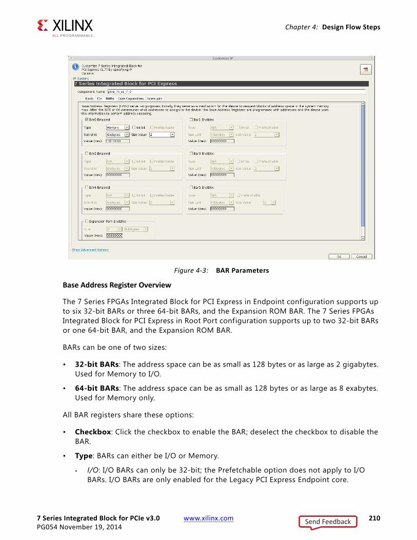
7 Series Integrated Block for PCIe v3.0 www.xilinx.com 210PG054 November 19, 2014
Chapter 4: Design Flow Steps
Base Address Register Overview
The 7 Series FPGAs Integrated Block for PCI Express in Endpoint configuration supports up to six 32-bit BARs or three 64-bit BARs, and the Expansion ROM BAR. The 7 Series FPGAs Integrated Block for PCI Express in Root Port configuration supports up to two 32-bit BARs or one 64-bit BAR, and the Expansion ROM BAR.
BARs can be one of two sizes:
• 32-bit BARs: The address space can be as small as 128 bytes or as large as 2 gigabytes. Used for Memory to I/O.
• 64-bit BARs: The address space can be as small as 128 bytes or as large as 8 exabytes. Used for Memory only.
All BAR registers share these options:
• Checkbox: Click the checkbox to enable the BAR; deselect the checkbox to disable the BAR.
• Type: BARs can either be I/O or Memory.
° I/O: I/O BARs can only be 32-bit; the Prefetchable option does not apply to I/O BARs. I/O BARs are only enabled for the Legacy PCI Express Endpoint core.
X-Ref Target - Figure 4-3
Figure 4-3: BAR Parameters
Send Feedback

7 Series Integrated Block for PCIe v3.0 www.xilinx.com 211PG054 November 19, 2014
Chapter 4: Design Flow Steps
° Memory: Memory BARs can be either 64-bit or 32-bit and can be prefetchable. When a BAR is set as 64 bits, it uses the next BAR for the extended address space and makes the next BAR inaccessible to you.
• Size: The available Size range depends on the PCIe® Device/Port Type and the Type of BAR selected. Table 4-5 lists the available BAR size ranges.
• Prefetchable: Identif ies the ability of the memory space to be prefetched.
• Value: The value assigned to the BAR based on the current selections.
For more information about managing the Base Address Register settings, see Managing Base Address Register Settings.
Expansion ROM Base Address Register
If selected, the Expansion ROM is activated and can be a value from 2 KB to 4 GB. According to the PCI 3.0 Local Bus Specification [Ref 2], the maximum size for the Expansion ROM BAR should be no larger than 16 MB. Selecting an address space larger than 16 MB might result in a non-compliant core.
Managing Base Address Register Settings
Memory, I/O, Type, and Prefetchable settings are handled by setting the appropriate settings for the desired base address register.
Memory or I/O settings indicate whether the address space is defined as memory or I/O. The base address register only responds to commands that access the specified address space. Generally, memory spaces less than 4 KB in size should be avoided. The minimum I/O space allowed is 16 bytes; use of I/O space should be avoided in all new designs.
Prefetchability is the ability of memory space to be prefetched. A memory space is prefetchable if there are no side effects on reads (that is, data is not destroyed by reading, as from a RAM). Byte write operations can be merged into a single double word write, when applicable.
When configuring the core as an Endpoint for PCIe (non-Legacy), 64-bit addressing must be supported for all BARs (except BAR5) that have the prefetchable bit set. 32-bit addressing is permitted for all BARs that do not have the prefetchable bit set. The prefetchable bit related requirement does not apply to a Legacy Endpoint. The minimum memory address
Table 4-5: BAR Size Ranges for Device Configuration
PCIe Device / Port Type BAR Type BAR Size Range
PCI Express Endpoint32-bit Memory 128 Bytes – 2 Gigabytes
64-bit Memory 128 Bytes – 8 Exabytes
Legacy PCI Express Endpoint
32-bit Memory 16 Bytes – 2 Gigabytes
64-bit Memory 16 Bytes – 8 Exabytes
I/O 16 Bytes – 2 Gigabytes
Send Feedback
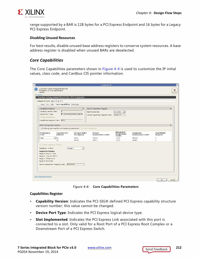
7 Series Integrated Block for PCIe v3.0 www.xilinx.com 212PG054 November 19, 2014
Chapter 4: Design Flow Steps
range supported by a BAR is 128 bytes for a PCI Express Endpoint and 16 bytes for a Legacy PCI Express Endpoint.
Disabling Unused Resources
For best results, disable unused base address registers to conserve system resources. A base address register is disabled when unused BARs are deselected.
Core Capabilities
The Core Capabilities parameters shown in Figure 4-4 is used to customize the IP initial values, class code, and Cardbus CIS pointer information.
Capabilities Register
• Capability Version: Indicates the PCI-SIG® defined PCI Express capability structure version number; this value cannot be changed.
• Device Port Type: Indicates the PCI Express logical device type.
• Slot Implemented: Indicates the PCI Express Link associated with this port is connected to a slot. Only valid for a Root Port of a PCI Express Root Complex or a Downstream Port of a PCI Express Switch.
X-Ref Target - Figure 4-4
Figure 4-4: Core Capabilities Parameters
Send Feedback
7 Series Integrated Block for PCIe v3.0 www.xilinx.com 213PG054 November 19, 2014
Chapter 4: Design Flow Steps
• Capabilities Register : Displays the value of the Capabilities register presented by the integrated block, and is not editable.
Device Capabilities Register
• Max Payload Size: Indicates the maximum payload size that the device/function can support for TLPs.
• Device Capabilities Register : Displays the value of the Device Capabilities register presented by the integrated block and is not editable.
Block RAM Configuration Options
• Buffering Optimized for Bus Mastering Applications: Causes the device to advertise to its Link Partner credit settings that are optimized for Bus Mastering applications.
• Performance Level: Selects the Performance Level settings, which determines the Receiver and Transmitter Sizes. The table displayed specifies the Receiver and Transmitter settings - number of TLPs buffered in the Transmitter, the Receiver Size, the Credits advertised by the Core to the Link Partner and the Number of Block RAMs required for the configuration, corresponding to the Max Payload Size selected, for each of the Performance Level options.
• Finite Completions: If selected, causes the device to advertise to the Link Partner the actual amount of space available for Completions in the Receiver. For an Endpoint, this is not compliant to the PCI Express Base Specification, rev. 2.1, as Endpoints are required to advertise an infinite amount of completion space.
Device Capabilities 2 Register
This section sets the Device Capabilities 2 register.
• Completion Timeout Disable Supported: Indicates support for Completion Timeout Disable mechanism
• Completion Timeout Ranges Supported: Indicates Device Function support for the optional Completion Timeout mechanism.
RECOMMENDED: Do not let the Completion Timeout mechanism expire in less than 10 ms.
• Device Capabilities2 Register: Displays the value of the Device Capabilities2 Register sent to the Core and is not editable.
Interrupts
The Interrupt parameters in Figure 4-5 sets the Legacy Interrupt Settings, and MSI Capabilities.
Send Feedback

7 Series Integrated Block for PCIe v3.0 www.xilinx.com 214PG054 November 19, 2014
Chapter 4: Design Flow Steps
Legacy Interrupt Settings
• Enable INTX: Enables the ability of the PCI Express function to generate INTx interrupts.
• Interrupt PIN: Indicates the mapping for Legacy Interrupt messages. A setting of “None” indicates no Legacy Interrupts are used.
Note: Only INT A is supported.
MSI Capabilities
• Enable MSI Capability Structure: Indicates that the MSI Capability structure exists.
• 64 bit Address Capable: Indicates that the function is capable of sending a 64-bit Message Address.
• Multiple Message Capable: Selects the number of MSI vectors to request from the Root Complex.
• Per Vector Masking Capable: Indicates that the function supports MSI per-vector Masking.
X-Ref Target - Figure 4-5
Figure 4-5: Interrupts Capabilities
Send Feedback
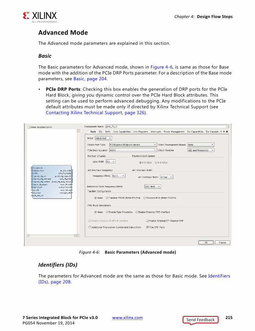
7 Series Integrated Block for PCIe v3.0 www.xilinx.com 215PG054 November 19, 2014
Chapter 4: Design Flow Steps
Advanced ModeThe Advanced mode parameters are explained in this section.
Basic
The Basic parameters for Advanced mode, shown in Figure 4-6, is same as those for Base mode with the addition of the PCIe DRP Ports parameter. For a description of the Base mode parameters, see Basic, page 204.
• PCIe DRP Ports: Checking this box enables the generation of DRP ports for the PCIe Hard Block, giving you dynamic control over the PCIe Hard Block attributes. This setting can be used to perform advanced debugging. Any modif ications to the PCIe default attributes must be made only if directed by Xilinx Technical Support (see Contacting Xilinx Technical Support, page 326).
Identifiers (IDs)
The parameters for Advanced mode are the same as those for Basic mode. See Identif iers (IDs), page 208.
X-Ref Target - Figure 4-6
Figure 4-6: Basic Parameters (Advanced mode)
Send Feedback
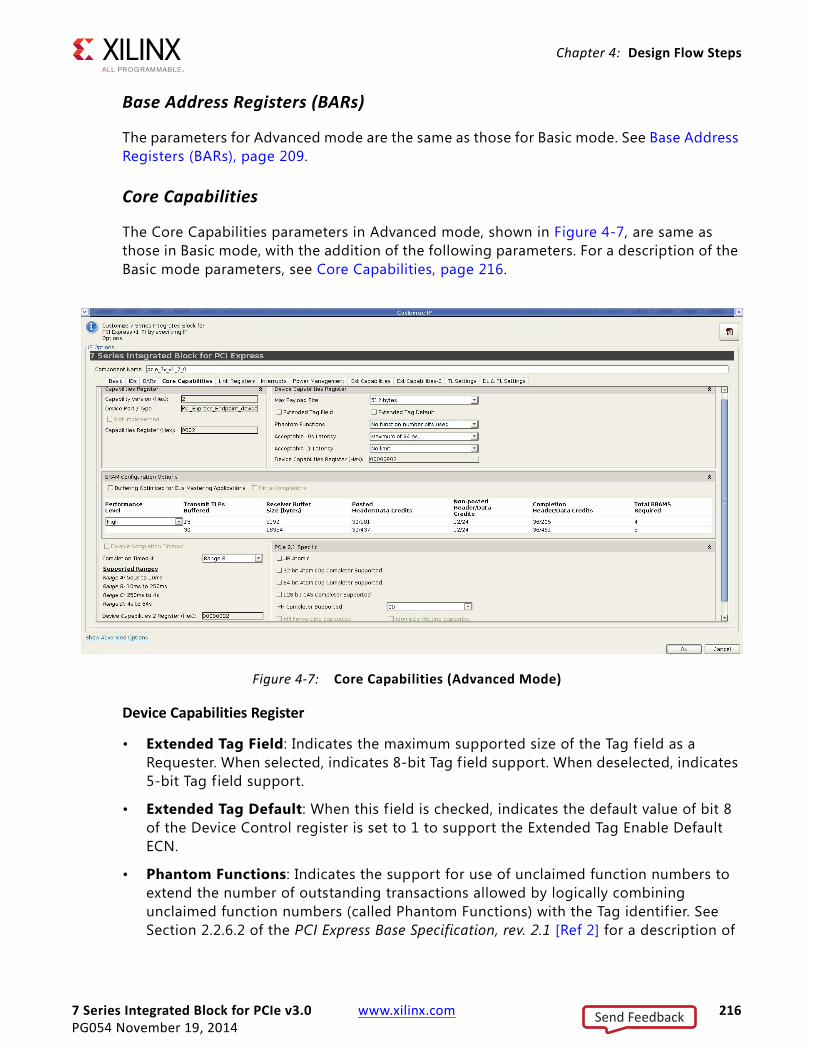
7 Series Integrated Block for PCIe v3.0 www.xilinx.com 216PG054 November 19, 2014
Chapter 4: Design Flow Steps
Base Address Registers (BARs)
The parameters for Advanced mode are the same as those for Basic mode. See Base Address Registers (BARs), page 209.
Core Capabilities
The Core Capabilities parameters in Advanced mode, shown in Figure 4-7, are same as those in Basic mode, with the addition of the following parameters. For a description of the Basic mode parameters, see Core Capabilities, page 216.
Device Capabilities Register
• Extended Tag Field: Indicates the maximum supported size of the Tag f ield as a Requester. When selected, indicates 8-bit Tag f ield support. When deselected, indicates 5-bit Tag f ield support.
• Extended Tag Default: When this f ield is checked, indicates the default value of bit 8 of the Device Control register is set to 1 to support the Extended Tag Enable Default ECN.
• Phantom Functions: Indicates the support for use of unclaimed function numbers to extend the number of outstanding transactions allowed by logically combining unclaimed function numbers (called Phantom Functions) with the Tag identif ier. See Section 2.2.6.2 of the PCI Express Base Specification, rev. 2.1 [Ref 2] for a description of
X-Ref Target - Figure 4-7
Figure 4-7: Core Capabilities (Advanced Mode)
Send Feedback

7 Series Integrated Block for PCIe v3.0 www.xilinx.com 217PG054 November 19, 2014
Chapter 4: Design Flow Steps
Tag Extensions. This f ield indicates the number of most signif icant bits of the function number portion of Requester ID that are logically combined with the Tag identif ier.
• Acceptable L0s Latency: Indicates the acceptable total latency that an Endpoint can withstand due to the transition from L0s state to the L0 state.
• Acceptable L1 Latency: Indicates the acceptable latency that an Endpoint can withstand due to the transition from L1 state to the L0 state.
Device Capabilities Register
• UR Atomic: If checked, the core automatically responds to Atomic Operation requests with an Unsupported Request. If unchecked, the core passes Atomic Operations TLPs to the user.
• 32-bit AtomicOp Completer Support: Indicates 32-bit AtomicOp Completer support.
• 64-bit AtomicOp Completer Support: Indicates 64-bit AtomicOp Completer support.
• 128-bit CAS Completer Support: Indicates 128-bit Compare And Swap completer support.
• TPH Completer Supported: Indicates the level of support for TPH completer.
Link Registers
The Link Registers page is available only when in Advanced mode.
X-Ref Target - Figure 4-8
Figure 4-8: Link Registers (Advanced Mode)
Send Feedback

7 Series Integrated Block for PCIe v3.0 www.xilinx.com 218PG054 November 19, 2014
Chapter 4: Design Flow Steps
Link Capabilities Register
This section sets the Link Capabilities register.
• Supported Link Speed: Indicates the supported link speed of the given PCI Express Link. This value is set to the Link Speed specif ied in the Basic tab and is not editable.
• Maximum Link Width: This value is set to the initial lane width specif ied in the Basic tab and is not editable.
• ASPM Optionality: When checked, this f ield enables ASPM optionally.
• DLL Link Active Reporting Capability: Indicates the optional Capability of reporting the DL_Active state of the Data Link Control and Management State Machine.
• Link Capabilities Register : Displays the value of the Link Capabilities register sent to the core and is not editable.
Link Control Register
• Hardware Autonomous Speed Disable: When checked, this f ield disables the hardware from changing the link speed for device specific reasons other than attempting to correct unreliable link operation by reducing link speed.
• Read Completion Boundary: Indicates the Read Completion Boundary for the Root Port.
• Target Link Speed: Sets an upper limit on the link operational speed. This is used to set the target Compliance Mode speed. The value is set to the supported link speed and can be edited only if the link speed is set to 5.0 Gb/s.
• Compliance De-emphasis: Sets the level of de-emphasis for an Upstream component, when the Link is operating at 5.0 Gb/s. This feature is not editable.
• Link Control Register 1: Displays the value of the Link Control Register sent to the core and is not editable.
• Link Control Register 2: Displays the value of the Link Control 2 Register sent to the core and is not editable.
Link Status Register
• Enable Slot Clock Configuration: Indicates that the Endpoint uses the platform-provided physical reference clock available on the connector. Must be cleared if the Endpoint uses an independent reference clock.
Configuration Register (Only in Root Port Configuration)
The Configuration Register pages isavailable only when Root Port configuration is selected, and when in Advanced mode.
Send Feedback

7 Series Integrated Block for PCIe v3.0 www.xilinx.com 219PG054 November 19, 2014
Chapter 4: Design Flow Steps
IMPORTANT: These settings are valid for Root Port configurations only.
Root Capabilities Register
• CRS Software Visibility: Indicates the Root Port capability of returning the CRs to software. When set, indicates that the Root Port can return the Configuration Request Retry Status (CRS) completion status to software.
• Root Capabilities Register : Specifies the Root Capabilities Register of the device.
Slot Control Capabilities Register
• Attention Button Present: Indicates the Attention Button is implemented. When set, indicates that an Attention Button for this slot is implemented on the chassis. This option is disabled when “Device_Port_Type” is not “Root Port of PCI Express Root Complex.” This is enabled only when the Slot Implemented parameter in the Core Capabilities tab is selected (see Figure 4-4).
• Attention Indicator Present: Indicates the Attention Indicator is implemented. When set, indicates that an Attention Indicator for this slot is implemented on the chassis. This option is disabled when “Device_Port_Type” is not “Root Port of PCI Express Root Complex.” This is enabled only when the Slot Implemented parameter in the Core Capabilities tab is selected (see Figure 4-4).
X-Ref Target - Figure 4-9
Figure 4-9: Config Register
Send Feedback

7 Series Integrated Block for PCIe v3.0 www.xilinx.com 220PG054 November 19, 2014
Chapter 4: Design Flow Steps
• Power Controller Present: Indicates the Power Controller is implemented. When set, indicates that a software programmable Power Controller is implemented for this slot. This option is disabled when “Device_Port_Type” is not “Root Port of PCI Express Root Complex.” This is enabled only when the Slot Implemented parameter in the Core Capabilities tab is selected (see Figure 4-4).
• Power Indicator Present: Indicates the Power Indicator is implemented. When set, indicates that a Power Indicator is implemented on the chassis for this slot. This option is disabled when “Device_Port_Type” is not “Root Port of PCI Express Root Complex.” This is enabled only when the Slot Implemented parameter in the Core Capabilities tab is selected (see Figure 4-4).
• Hot-Plug Surprise: When set, indicates that an adapter in this slot might be removed from the system without any prior notif ication. This option is disabled when “Device_Port_Type” is not “Root Port of PCI Express Root Complex.” This is enabled only when the Slot Implemented parameter in the Core Capabilities tab is selected (see Figure 4-4).
• Hot-Plug Capable: When set, indicates that this slot is capable of supporting hot-plug operations. This option is disabled when "Device_Port_Type" is not “ Root Port of PCI Express Root Complex.” This is enabled only when the Slot Implemented parameter in the Core Capabilities tab is selected (see Figure 4-4).
• MRL Sensor Present: Indicates MRL Sensor implemented. When Set, indicates that an MRL (Manually operated Retention Latch) sensor is implemented for this slot, on the chassis. This option is disabled when “Device_Port_Type” is not “Root Port of PCI Express Root Complex.” This is enabled only when the Slot Implemented parameter in the Core Capabilities tab is selected (see Figure 4-4).
• Electromechanical Interlock Present: When set, indicates that an Electromechanical Interlock is implemented on the chassis for this slot. This option is disabled when "Device_Port_Type" is not “Root Port of PCI Express Root Complex.” This is enabled only when the Slot Implemented parameter in the Core Capabilities tab is selected (see Figure 4-4).
• No Command Completed Support: When set, indicates that the slot does not generate software notif ication when an issue command is completed by the Hot-Plug Controller. This option is disabled when "Device_Port_Type" is not “Root Port of PCI Express Root Complex.” This is enabled only when the Slot Implemented parameter in the Core Capabilities tab is selected (see Figure 4-4).
• Slot Power Limit Value: Specif ies the Upper Limit on power supplied to the slot, in combination with Slot Power Limit Scale value. This option is disabled when "Device_Port_Type" is not “Root Port of PCI Express Root Complex.” This is enabled only when the Slot Implemented parameter in the Core Capabilities tab is selected (see Figure 4-4).
• Slot Power Limit Scale: Specif ies the scale used for the Slot Power Limit value. This option is disabled when "Device_Port_Type" is not “Root Port of PCI Express Root Complex.” This is enabled only when the Slot Implemented parameter in the Core
Send Feedback

7 Series Integrated Block for PCIe v3.0 www.xilinx.com 221PG054 November 19, 2014
Chapter 4: Design Flow Steps
Capabilities tab is selected (see Figure 4-4).
• Physical Slot Number : Specif ies the Physical Slot Number attached to this port. This f ield must be hardware initialized to a value that assigns a slot number that is unique within the chassis, regardless of form factor associated with the slot. This option is disabled when "Device_Port_Type" is not “Root Port of PCI Express Root Complex.” This is enabled only when the Slot Implemented parameter in the Core Capabilities tab is selected (see Figure 4-4).
• Slot Capabilities Register. Specifies the Slot Capabilities Register of the device.
Interrupts
The Interrupts parameters in Advanced mode are the same as those in Basic mode, with the addition of MSIx Capabilities. For a description of the Basic mode parameters, see Interrupts, page 213.
MSI-X Capabilities
• Enable MSIx Capability Structure: Indicates that the MSI-X Capability structure exists.
Note: This Capability Structure needs at least one Memory BAR to be configured.
• MSIx Table Settings: Defines the MSI-X Table Structure.
° Table Size: Specifies the MSI-X Table Size.
° Table Offset: Specif ies the Offset from the Base Address Register that points to the Base of the MSI-X Table.
X-Ref Target - Figure 4-10
Figure 4-10: Interrupts Parameters (Advanced Mode)
Send Feedback
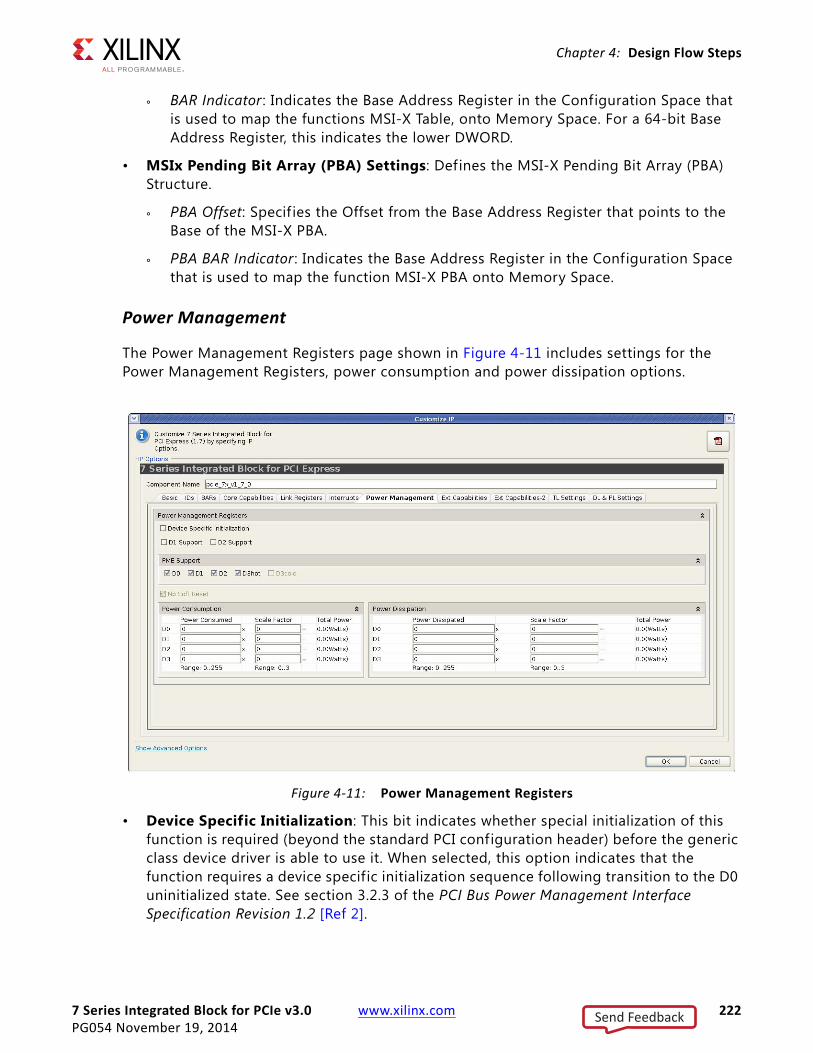
7 Series Integrated Block for PCIe v3.0 www.xilinx.com 222PG054 November 19, 2014
Chapter 4: Design Flow Steps
° BAR Indicator : Indicates the Base Address Register in the Configuration Space that is used to map the functions MSI-X Table, onto Memory Space. For a 64-bit Base Address Register, this indicates the lower DWORD.
• MSIx Pending Bit Array (PBA) Settings: Defines the MSI-X Pending Bit Array (PBA) Structure.
° PBA Offset: Specif ies the Offset from the Base Address Register that points to the Base of the MSI-X PBA.
° PBA BAR Indicator : Indicates the Base Address Register in the Configuration Space that is used to map the function MSI-X PBA onto Memory Space.
Power Management
The Power Management Registers page shown in Figure 4-11 includes settings for the Power Management Registers, power consumption and power dissipation options.
• Device Specific Initialization: This bit indicates whether special initialization of this function is required (beyond the standard PCI configuration header) before the generic class device driver is able to use it. When selected, this option indicates that the function requires a device specific initialization sequence following transition to the D0 uninitialized state. See section 3.2.3 of the PCI Bus Power Management Interface Specification Revision 1.2 [Ref 2].
X-Ref Target - Figure 4-11
Figure 4-11: Power Management Registers
Send Feedback

7 Series Integrated Block for PCIe v3.0 www.xilinx.com 223PG054 November 19, 2014
Chapter 4: Design Flow Steps
• D1 Support: When selected, this option indicates that the function supports the D1 Power Management State. See section 3.2.3 of the PCI Bus Power Management Interface Specification Revision 1.2.
• D2 Support: When selected, this option indicates that the function supports the D2 Power Management State. See section 3.2.3 of the PCI Bus Power Management Interface Specification Revision 1.2.
• PME Support From: When this option is selected, it indicates the power states in which the function can assert cfg_pm_wake. See section 3.2.3 of the PCI Bus Power Management Interface Specification Revision 1.2.
• No Soft Reset: Checking this box indicates that if the device transitions from D3hot to D0 because of a Power State Command, it does not perform an internal reset and Configuration context is preserved. Disabling this option is not supported.
Power Consumption
The 7 Series FPGAs Integrated Block for PCI Express always reports a power budget of 0W. For information about power consumption, see section 3.2.6 of the PCI Bus Power Management Interface Specification Revision 1.2.
Power Dissipated
The 7 Series FPGAs Integrated Block for PCI Express always reports a power dissipation of 0W. For information about power dissipation, see section 3.2.6 of the PCI Bus Power Management Interface Specification Revision 1.2.
Extended Capabilities
The PCIe Extended Capabilities page shown in Figure 4-12 is available in Advanced mode only, and includes settings for Device Serial Number Capability, Virtual Channel Capability, Vendor Specif ic Capability, and optional user-defined Configuration capabilities.
Send Feedback

7 Series Integrated Block for PCIe v3.0 www.xilinx.com 224PG054 November 19, 2014
Chapter 4: Design Flow Steps
Device Serial Number Capability
• Device Serial Number Capability: An optional PCIe Extended Capability containing a unique Device Serial Number. When this Capability is enabled, the DSN identif ier must be presented on the Device Serial Number input pin of the port. This Capability must be turned on to enable the Virtual Channel and Vendor Specific Capabilities.
Virtual Channel Capability
• Virtual Channel Capability: An optional PCIe Extended Capability which allows the user application to be operated in TCn/VC0 mode. Checking this allows Traffic Class f iltering to be supported.
• Reject Snoop Transactions (Root Port Configuration Only): When enabled, any transactions for which the No Snoop attribute is applicable, but is not set in the TLP header, can be rejected as an Unsupported Request.
Vendor Specific Capability
• Vendor Specific Capability: An optional PCIe Extended Capability that allows PCI Express component vendors to expose Vendor Specific Registers. When checked, enables Xilinx specific Loopback Control.
X-Ref Target - Figure 4-12
Figure 4-12: PCIe Extended Capabilities
Send Feedback

7 Series Integrated Block for PCIe v3.0 www.xilinx.com 225PG054 November 19, 2014
Chapter 4: Design Flow Steps
User-Defined Configuration Capabilities: Endpoint Configuration Only
• PCI Configuration Space Enable: Allows the user application to add/implement PCI Legacy capability registers. This option should be selected if the user application implements a legacy capability configuration space. This option enables the routing of Configuration Requests to addresses outside the built-in PCI-Compatible Configuration Space address range to the AXI4-Stream interface.
• PCI Configuration Space Pointer : Sets the starting Dword aligned address of the user-definable PCI Compatible Configuration Space. The available DWORD address range is 2Ah - 3Fh.
• PCI Express Extended Configuration Space Enable: Allows the user application to add/implement PCI Express Extended capability registers. This option should be selected if the user application implements such an extended capability configuration space. This enables the routing of Configuration Requests to addresses outside the built-in PCI Express Extended Configuration Space address range to the user application.
• PCI Configuration Space Pointer : Sets the starting DWORD aligned address of the PCI Express Extended Configuration Space implemented by the user application. This action enables routing of Configuration Requests with DWORD addresses greater than or equal to the value set in the user application. The available address range depends on the PCIe Extended Capabilities selected. For more information, see Chapter 3, Designing with the Core.
Extended Capabilities 2
The Extended Capabilities 2 page is available only when in Advanced mode.
Send Feedback

7 Series Integrated Block for PCIe v3.0 www.xilinx.com 226PG054 November 19, 2014
Chapter 4: Design Flow Steps
AER Capability
• Enable AER Capability: An optional PCIe Extended Capability that allows Advanced Error Reporting.
• Multiheader : Indicates support for multiple-header buffering for the AER header log f ield. (Not supported for the 7 Series FPGAs Integrated Block for PCI Express.)
• Permit Root Error Update: If TRUE, permits the AER Root Status and Error Source ID registers to be updated. If FALSE, these registers are forced to 0.
• ECRC Check Capable: Indicates the core can check ECRC.
• Optional Error Support: Indicates which option error conditions in the Uncorrectable and Correctable Error Mask/Severity registers are supported. If an error box is unchecked, the corresponding bit in the Mask/Severity register is hardwired to 0.
X-Ref Target - Figure 4-13
Figure 4-13: PCIe Extended Capabilities: AER Capability
Send Feedback

7 Series Integrated Block for PCIe v3.0 www.xilinx.com 227PG054 November 19, 2014
Chapter 4: Design Flow Steps
RBAR Capabilities
• Enable RBAR Capability: An optional PCIe Extended Capability that allows Resizable BARs.
• Number of RBARs: Number of resizeable BARs in the Cap Structure, which depends on the number of BARs enabled.
• BARn Size Supported: RBAR Size Supported vector for RBAR Capability Register (0 through 5)
• BARn Index Value: Sets the index of the resizeable BAR from among the enabled BARs
• RBARn Init Value: RBAR Initial Value for the RBAR Control BAR Size f ield.
ECRC
• Receive ECRC Check : Enables ECRC checking of received TLPs.
° 0 = Do not check
° 1 = Always check
° 3 = Check if enabled by the ECRC check enable bit of the AER Capability Structure
• Trim TLP Digest: Enables TD bit clear and ECRC trim on received TLPs.
• Disable RX Poisoned Resp: Disables the core from sending a message and setting status bits due to receiving a Poisoned TLP. The behavior of the core when the Disable RX poisoned Resp is checked is as follows.
° When Advisory Non-Fatal Error Mask: 1 (default). When the core Receives a poisoned CfgWr, it sets Parity Error and sends completion with UR. When it receives poisoned MemWr, it sets the Parity error and no TLP is sent.
X-Ref Target - Figure 4-14
Figure 4-14: PCIe Extended Capabilities: RBAR Capabilities
X-Ref Target - Figure 4-15
Figure 4-15: PCIe Extended Capabilities: ECRC
Send Feedback

7 Series Integrated Block for PCIe v3.0 www.xilinx.com 228PG054 November 19, 2014
Chapter 4: Design Flow Steps
° Advisory Non-Fatal Error Mask: 0. When DISABLE_RX_POISONED_RESP is set to FALSE and a poisoned MemWr is received, the core sends an error message automatically. When DISABLE_RX_POISONED_RESP is set to TRUE and a poisoned MemWr is received, an error message is not transmitted. When you assert cfg_err_poisoned, the core sends the error message.
TL Settings
The Transaction Layer (TL) Settings page is available only when in Advanced mode.
Transaction Layer Module
• Enable Message Routing: Controls if message TLPs are also received on the AXI4-Stream interface.
• Endpoint:
° Unlock and PME_Turn_Off Messages
• Root Port:
° Error Messages - Error Correctable, Error Non-Fatal, Error Fatal
° Assert/Deassert INT Messages - INTA, INTB, INTC, INTD
° Power Management Messages - PM_PME, PME_TO_ACK
X-Ref Target - Figure 4-16
Figure 4-16: TL Settings
Send Feedback

7 Series Integrated Block for PCIe v3.0 www.xilinx.com 229PG054 November 19, 2014
Chapter 4: Design Flow Steps
• Receive Non-Posted Request (Non-Posted Flow Control)
° The rx_np_req signal prevents the user application from buffering Non-Posted TLPs. When rx_np_req is asserted, one Non-Posted TLP is requested from the integrated block. This signal cannot be used in conjunction with rx_np_ok . Every time that rx_np_req is asserted, one TLP is presented on the receive interface; whereas, every time that rx_np_ok is deasserted, the user application needs to buffer up to two additional Non-Posted TLPs.
• Pipeline Registers for Transaction Block RAM Buffers: Selects the Pipeline registers enabled for the Transaction Buffers. Pipeline registers can be enabled on either the Write path or both the Read and Write paths of the Transaction Block RAM buffers.
• ATS
° UR_INV_REQ: When this box is checked, the core handles received ATS Invalidate request messages as unsupported requests. When this box is unchecked, the core passes received ATS Invalidate request messages.
° UR_PRS_RESPONSE: When this box is checked, the core handles received ATS Page Request Group Response messages as unsupported requests. When this box is unchecked, the core passes received ATS PRG Response messages.
DL and PL Settings
The DL and PL Settings page is available only when in Advanced mode.
X-Ref Target - Figure 4-17
Figure 4-17: DL and PL Settings
Send Feedback
7 Series Integrated Block for PCIe v3.0 www.xilinx.com 230PG054 November 19, 2014
Chapter 4: Design Flow Steps
Link Layer Module
• Override ACK/NAK Latency Timer : Checking this box enables you to override the ACK/NAK latency timer values set in the device. Using this feature can cause the ACK timeout values to be non-compliant to the PCI Express Base Specification, rev. 2.1 [Ref 2]. This setting can be used to perform advanced debugging operations.
CAUTION! Modify the default attributes only if directed by Xilinx Technical Support.
• ACK Latency Timer Override Function: This setting determines how the override value is used by the device with respect to the ACK/NAK Latency Timer Value in the device. Options are “Absolute”, “Add”, and “Subtract”. The f irst two settings can cause the ACK timeout values to be non-compliant with the PCI Express Base Specification, rev. 2.1.
• ACK Latency Timer Override Value: This setting determines the ACK/NAK latency timer value used by the device depending on if the ACK Latency Timer Override Function enabled. The built-in table value depends on the Negotiated Link Width and Programmed MPS of the device.
• Override Replay Timer : Checking this box enables you to override the replay timer values set in the device. Use of this feature could cause the replay timeout values to be non-compliant to the PCI Express Base Specification, rev. 2.1. This setting can be used to perform advanced debugging operations.
CAUTION! Modify the default attributes only if directed by Xilinx Technical Support.
• Replay Timer Override Function: This setting determines how the override value is used by the device with respect to the replay timer value in the device. Options are “Absolute”, “Add”, and “Subtract”. The first two settings can cause the replay timeout values to be non-compliant with the PCI Express Base Specification, rev. 2.1.
• Replay Timer Override Value: This setting determines the replay timer value used by the device depending on if the Replay Timer Override Function enabled. The built-in table value depends on the Negotiated Link Width and Programmed MPS of the device.
IMPORTANT: You must ensure that the final timeout value does not overflow the 15-bit timeout value.
Advanced Physical Layer
• Enable Lane Reversal: When checked, enables the Lane Reversal feature.
• Force No Scrambling: Used for diagnostic purposes only and should never be enabled in a working design. Setting this bit results in the data scramblers being turned off so that the serial data stream can be analyzed.
• Upconfigure Capable: When unchecked, the port is advertised as “Not Upconfigure Capable” during Link Training.
Send Feedback
7 Series Integrated Block for PCIe v3.0 www.xilinx.com 231PG054 November 19, 2014
Chapter 4: Design Flow Steps
• Disable TX ASPM L0s: When checked, prevents the device transmitter from entering the L0s state.
RECOMMENDED: Disable TX ASPM L0s for a link that interconnects a 7 series FPGA to any Xilinx component.
• Link Number : Specifies the link number advertised by the device in TS1 and TS2 ordered sets during Link training. Used in downstream facing mode only.
Shared Logic
Enables you to share common blocks across multiple instantiations by selecting one or more of the options on this page. For a details description of the shared logic feature, see Shared Logic in Chapter 3.
Core Interface Parameters
You can select the core interface parameters to use. By default all ports are brought out. For cases you might choose to disable some of the interfaces if they are not used. When disabled, the interfaces (ports) are removed from the core top.
RECOMMENDED: For a typical use case, do not disable the interfaces. Disable the ports only in special cases.
Send Feedback

7 Series Integrated Block for PCIe v3.0 www.xilinx.com 232PG054 November 19, 2014
Chapter 4: Design Flow Steps
PL Interface
When you disable the physical layer (PL) Interface option, the following ports are removed from the core. This option enables you to inspect the status of the link and link partner and control the link state
• pl_sel_lnk_rate
• pl_sel_lnk_width
• pl_ltssm_state
• pl_lane_reversal_mode
• pl_phy_lnk_up
• pl_directed_link_change
X-Ref Target - Figure 4-18
Figure 4-18: Core Interface Parameters
Send Feedback
7 Series Integrated Block for PCIe v3.0 www.xilinx.com 233PG054 November 19, 2014
Chapter 4: Design Flow Steps
• pl_directed_link_width
• pl_directed_link_speed
• pl_directed_link_auton
• pl_tx_pm_state
• pl_rx_pm_state
• pl_link_upcfg_cap
• pl_link_gen2_cap
• pl_link_partner_gen2_supported
• pl_initial_link_width
• pl_upstream_prefer_deemph
• pl_downstream_deemph_source
• pl_directed_change_done
• pl_transmit_hot_rst
• pl_received_hot_rst
Error Reporting
When you disable the Error Reporting option, the following ports are removed from the core. These signals are associated with the user application error reporting interface for the PCIe Gen2 core.
• cfg_err_malformed
• cfg_err_cor
• cfg_err_ur
• cfg_err_ecrc
• cfg_err_cpl_timeout
• cfg_err_cpl_abort
• cfg_err_cpl_unexpect
• cfg_err_poisoned
• cfg_err_acs
• cfg_err_atomic_egress_blocked
• cfg_err_mc_blocked
• cfg_err_internal_uncor
• cfg_err_internal_cor
Send Feedback

7 Series Integrated Block for PCIe v3.0 www.xilinx.com 234PG054 November 19, 2014
Chapter 4: Design Flow Steps
• cfg_err_posted
• cfg_err_locked
• cfg_err_norecovery
• cfg_err_cpl_rdy
• cfg_err_tlp_cpl_header
• cfg_err_aer_headerlog
• cfg_aer_interrupt_msgnum
• cfg_err_aer_headerlog_set
• cfg_aer_ecrc_check_en
• cfg_aer_ecrc_gen_en
Config Management Interface
When you disable the Config Management Interface option, the following ports are removed from the port. These signals are used to read and write to the Configuration Space registers.
• cfg_mgmt_do
• cfg_mgmt_di
• cfg_mgmt_byte_en
• cfg_mgmt_dwaddr
• cfg_mgmt_wr_rw1c_as_rw
• cfg_mgmt_wr_readonly
• cfg_mgmt_wr_en
• cfg_mgmt_rd_en
• cfg_mgmt_rd_wr_done
Config CTRL Interface
When you disable the Config Control (CTRL) Interface option, the following ports are removed from the core. These signals allow a broad range of information exchange between the user application and the core.
• cfg_trn_pending
• cfg_pm_halt_aspm_l0s
• cfg_pm_halt_aspm_l1
• cfg_pm_force_state_en
Send Feedback
7 Series Integrated Block for PCIe v3.0 www.xilinx.com 235PG054 November 19, 2014
Chapter 4: Design Flow Steps
• cfg_pm_force_state
• cfg_dsn
• tx_cfg_gnt
• rx_np_ok
• rx_np_req
• cfg_turnoff_ok
• cfg_pm_wake
• cfg_pm_send_pme_to
• cfg_ds_bus_number
• cfg_ds_device_number
• cfg_ds_function_number
Config Status Interface
When you disable the Config Status Interface, the following ports are removed from the core. These signals provide information on how the PCIe Gen2 core is configured.
• cfg_status
• cfg_command
• cfg_dstatus
• cfg_dcommand
• cfg_lstatus
• cfg_lcommand
• cfg_dcommand2
• cfg_pcie_link_state
• cfg_pmcsr_powerstate
• cfg_pmcsr_pme_en
• cfg_pmcsr_pme_status
• cfg_received_func_lvl_rst
• cfg_to_turnoff
• cfg_bus_number
• cfg_device_number
• cfg_function_number
• cfg_bridge_serr_en
Send Feedback

7 Series Integrated Block for PCIe v3.0 www.xilinx.com 236PG054 November 19, 2014
Chapter 4: Design Flow Steps
• cfg_slot_control_electromech_il_ctl_pulse
• cfg_root_control_syserr_corr_err_en
• cfg_root_control_syserr_non_fatal_err_en
• cfg_root_control_syserr_fatal_err_en
• cfg_root_control_pme_int_en
• cfg_aer_rooterr_corr_err_reporting_en
• cfg_aer_rooterr_non_fatal_err_reporting_en
• cfg_aer_rooterr_fatal_err_reporting_en
• cfg_aer_rooterr_corr_err_received
• cfg_aer_rooterr_non_fatal_err_received
• cfg_aer_rooterr_fatal_err_received
• cfg_vc_tcvc_map
• tx_buf_av
• tx_err_drop
• tx_cfg_req
Receive Msg Interface
When you disable the Receive Message Interface option, the following ports are removed from the core. These signals indicate decodable messages from the link, parameters associated with the data, and type of message received.
• cfg_msg_received
• cfg_msg_data
• cfg_msg_received_err_cor
• cfg_msg_received_err_non_fatal
• cfg_msg_received_err_fatal
• cfg_msg_received_assert_int_a
• cfg_msg_received_deassert_int_a
• cfg_msg_received_assert_int_b
• cfg_msg_received_deassert_int_b
• cfg_msg_received_assert_int_c
• cfg_msg_received_deassert_int_c
• cfg_msg_received_assert_int_d
Send Feedback
7 Series Integrated Block for PCIe v3.0 www.xilinx.com 237PG054 November 19, 2014
Chapter 4: Design Flow Steps
• cfg_msg_received_deassert_int_d
• cfg_msg_received_pm_pme
• cfg_msg_received_pme_to_ack
• cfg_msg_received_unlock
• cfg_msg_received_pm_as_nak
Config FC Interface
When you disable the Config flow control (FC) Interface option, the following ports are removed from the core. These signals are associated with the configuration flow control for the PCIe Gen2 Core.
• cfg_fc_ph
• cfg_fc_pd
• cfg_fc_nph
• cfg_fc_npd
• cfg_fc_cplh
• cfg_fc_cpld
• cfg_fc_sel
Output GenerationFor details, see the Vivado Design Suite User Guide: Designing with IP (UG896) [Ref 14].
Endpoint Configuration
This section shows the directory structure for the Endpoint configuration of the generated core. See Chapter 5, Detailed Example Designs for descriptions of the contents of each directory.
Send Feedback

7 Series Integrated Block for PCIe v3.0 www.xilinx.com 238PG054 November 19, 2014
Chapter 4: Design Flow Steps
Root Port Configuration
This section shows the directory structure for the Root Port configuration of the generated core. See Chapter 5, Detailed Example Designs for descriptions of the contents of each directory.
X-Ref Target - Figure 4-19
Figure 4-19: Endpoint Configuration Directory Structure
Send Feedback

7 Series Integrated Block for PCIe v3.0 www.xilinx.com 239PG054 November 19, 2014
Chapter 4: Design Flow Steps
Constraining the CoreThe 7 Series FPGAs Integrated Block for PCI Express solution requires the specification of timing and other physical implementation constraints to meet specified performance requirements for PCI Express. These constraints are provided with the Endpoint and Root Port solutions in a Xilinx Design Constraints (XDC) file. Pinouts and hierarchy names in the generated XDC correspond to the provided example design.
TIP: To achieve consistent implementation results, use an XDC file containing these original, unmodified constraints when a design is run through the Xilinx tools. For additional details on the definition and use of an XDC file or specific constraints, see the Vivado Design Suite Tcl Command Reference Guide (UG835) [Ref 19].
Constraints provided with the integrated block solution have been tested in hardware and provide consistent results. Constraints can be modif ied, but modif ications should only be made with a thorough understanding of the effect of each constraint. Additionally, support is not provided for designs that deviate from the provided constraints.
Although the XDC file delivered with each core shares the same overall structure and sequence of information, the content of the XDC for each core varies. The sections that follow define the structure and sequence of information in a generic XDC.
X-Ref Target - Figure 4-20
Figure 4-20: Root Port Configuration Directory Structure
Send Feedback
7 Series Integrated Block for PCIe v3.0 www.xilinx.com 240PG054 November 19, 2014
Chapter 4: Design Flow Steps
Device, Package, and Speed Grade SelectionsThe first section of the XDC specif ies the exact device for the implementation tools to target, including the specific part, package, and speed grade. In some cases, device-specif ic options can be included. The device in the XDC reflects the device chosen in the Vivado Design Suite project.
User Timing Constraints
The user timing constraints section is not populated. It is a placeholder for you to provide timing constraints on user-implemented logic.
User Physical Constraints
The user physical constraints section is not populated. It is a placeholder for you to provide physical constraints on user-implemented logic.
Core Pinout and I/O Constraints
The core pinout and I/O constraints section contains constraints for I/Os belonging to the core System (SYS) and PCI Express (PCI_EXP) interfaces. It includes location constraints for pins, I/O logic and I/O standard constraints.
Core Physical Constraints
The core physical constraints are used to limit the core to a specif ic area of the device and to specify locations for clock buffering and other logic instantiated by the core.
Core Timing Constraints
This core timing constraints section defines clock frequency requirements for the core and specifies which nets the timing analysis tool should ignore.
Device Selection
The device selection portion of the XDC informs the implementation tools which part, package, and speed grade to target for the design.
IMPORTANT: Because the core is designed for specific part and package combinations, do not modify this section.
The device selection section always contains a part selection line, but can also contain part or package-specific options. An example part selection line:
CONFIG PART = XC7V585T-FFG1761-1
Send Feedback
7 Series Integrated Block for PCIe v3.0 www.xilinx.com 241PG054 November 19, 2014
Chapter 4: Design Flow Steps
Core I/O AssignmentsThis section controls the placement and options for I/Os belonging to the core System (SYS) interface and PCI Express (PCI_EXP) interface. set_property constraints in this section control the pin location and I/O options for signals in the SYS group. Locations and options vary depending on which derivative of the core is used and should not be changed without fully understanding the system requirements.
For example:
set_property IOSTANDARD LVCMOS18 [get_ports sys_rst_n]set_property LOC IBUFDS_GTE2_X0Y3 [get_cells refclk_ibuf]
See Clocking and Resets in Chapter 3 for detailed information about reset and clock requirements.
For GTX transceiver pinout information, see the “Placement Information by Package” appendix in the 7 Series FPGAs GTX/GTH Transceivers User Guide (UG476) [Ref 12].
INST constraints are used to control placement of signals that belong to the PCI_EXP group. These constraints control the location of the transceiver(s) used, which implicitly controls pin locations for the transmit and receive differential pair.
For example:
set_property LOC GTXE2_CHANNEL_X0Y7 [get_cells {pcie_7x_v2_1_0_i/inst/inst/gt_top_i/pipe_wrapper_i/pipe_lane[0].gt_wrapper_i/gtx_channel.gtxe2_channel_i}]
Core Physical ConstraintsCore physical constraints are included in the constraints f ile to control the location of clocking and other elements and to limit the core to a specif ic area of the FPGA logic.
IMPORTANT: Specific physical constraints are chosen to match each supported device and package combination. Do not modify these constraints.
Note: In certain situations where a design cannot close timing, the following AREA_GROUP constraints can be added to XDC.
INST "core/*" AREA_GROUP = "AG_core" ;AREA_GROUP "AG_core" RANGE = SLICE_X136Y147:SLICE_X155Y120 ;
Send Feedback

7 Series Integrated Block for PCIe v3.0 www.xilinx.com 242PG054 November 19, 2014
Chapter 4: Design Flow Steps
Core Timing ConstraintsTiming constraints are provided for all integrated block solutions, although they differ based on core configuration. In all cases, they are crucial and must not be modified, except to specify the top-level hierarchical name. Timing constraints are divided into two categories:
• set_false_path constraints. Used on paths where specif ic delays are unimportant, to instruct the timing analysis tools to refrain from issuing Unconstrained Path warnings.
• Frequency constraints. Group clock nets into time groups and assign properties and requirements to those groups.
Here is an example of a set_false_path constraint:
set_false_path -from [get_ports sys_rst_n]
Clock constraints example:
First, the input reference clock period is specif ied, which can be 100 MHz, 125 MHz, or 250 MHz (selected in the Vivado IDE).
create_clock -name sys_clk -period 10 [get_pins refclk_ibuf/O]
Next, the internally generated clock net and period are specif ied, which can be 100 MHz, 125 MHz, or 250 MHz.
Note: Both clock constraints must be specif ied as 100 MHz, 125 MHz, or 250 MHz.
create_generated_clock -name clk_125mhz -source [get_pins refclk_ibuf/O] -edges {1 2 3} -edge_shift {0 -1 -2} [get_pins ext_clk.pipe_clock_i/mmcm_i/CLKOUT0]
create_generated_clock -name clk_userclk -source [get_pins refclk_ibuf/O] -edges {1 2 3} -edge_shift {0 3 6} [get_pins ext_clk.pipe_clock_i/mmcm_i/CLKOUT2]
Relocating the Integrated Block CoreWhile Xilinx does not provide technical support for designs whose system clock input, GTXE transceivers, or block RAM locations are different from the provided examples, it is possible to relocate the core within the FPGA. The locations selected in the examples provided are the recommended pinouts. These locations have been chosen based on the proximity to the PCIe® block, which enables meeting 250 MHz timing, and because they are conducive to layout requirements for add-in card design. If the core is moved, the relative location of all transceivers and clocking resources should be maintained to ensure timing closure.
Send Feedback
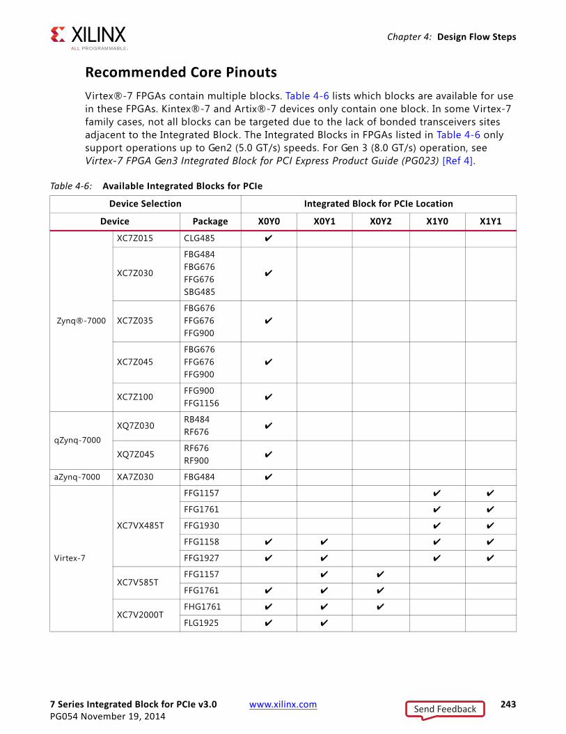
7 Series Integrated Block for PCIe v3.0 www.xilinx.com 243PG054 November 19, 2014
Chapter 4: Design Flow Steps
Recommended Core PinoutsVirtex®-7 FPGAs contain multiple blocks. Table 4-6 lists which blocks are available for use in these FPGAs. Kintex®-7 and Artix®-7 devices only contain one block. In some Virtex-7 family cases, not all blocks can be targeted due to the lack of bonded transceivers sites adjacent to the Integrated Block. The Integrated Blocks in FPGAs listed in Table 4-6 only support operations up to Gen2 (5.0 GT/s) speeds. For Gen 3 (8.0 GT/s) operation, see Virtex-7 FPGA Gen3 Integrated Block for PCI Express Product Guide (PG023) [Ref 4].
Table 4-6: Available Integrated Blocks for PCIe
Device Selection Integrated Block for PCIe Location
Device Package X0Y0 X0Y1 X0Y2 X1Y0 X1Y1
Zynq®-7000
XC7Z015 CLG485 ✔
XC7Z030
FBG484FBG676FFG676SBG485
✔
XC7Z035FBG676FFG676FFG900
✔
XC7Z045FBG676FFG676FFG900
✔
XC7Z100FFG900FFG1156
✔
qZynq-7000
XQ7Z030RB484RF676
✔
XQ7Z045RF676RF900
✔
aZynq-7000 XA7Z030 FBG484 ✔
Virtex-7
XC7VX485T
FFG1157 ✔ ✔
FFG1761 ✔ ✔
FFG1930 ✔ ✔
FFG1158 ✔ ✔ ✔ ✔
FFG1927 ✔ ✔ ✔ ✔
XC7V585TFFG1157 ✔ ✔
FFG1761 ✔ ✔ ✔
XC7V2000TFHG1761 ✔ ✔ ✔
FLG1925 ✔ ✔
Send Feedback
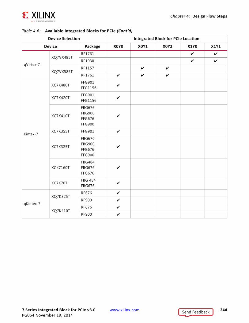
7 Series Integrated Block for PCIe v3.0 www.xilinx.com 244PG054 November 19, 2014
Chapter 4: Design Flow Steps
qVirtex-7
XQ7VX485TRF1761 ✔ ✔
RF1930 ✔ ✔
XQ7VX585TRF1157 ✔ ✔
RF1761 ✔ ✔ ✔
Kintex-7
XC7K480TFFG901FFG1156
✔
XC7K420TFFG901FFG1156
✔
XC7K410T
FBG676FBG900FFG676FFG900
✔
XC7K355T FFG901 ✔
XC7K325T
FBG676FBG900FFG676FFG900
✔
XCK7160TFBG484FBG676FFG676
✔
XC7K70TFBG 484FBG676
✔
qKintex-7
XQ7K325TRF676 ✔
RF900 ✔
XQ7K410TRF676 ✔
RF900 ✔
Table 4-6: Available Integrated Blocks for PCIe (Cont’d)
Device Selection Integrated Block for PCIe Location
Device Package X0Y0 X0Y1 X0Y2 X1Y0 X1Y1
Send Feedback
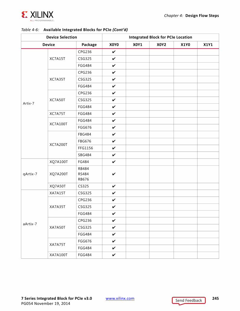
7 Series Integrated Block for PCIe v3.0 www.xilinx.com 245PG054 November 19, 2014
Chapter 4: Design Flow Steps
Artix-7
XC7A15T
CPG236 ✔
CSG325 ✔
FGG484 ✔
XC7A35T
CPG236 ✔
CSG325 ✔
FGG484 ✔
XC7A50T
CPG236 ✔
CSG325 ✔
FGG484 ✔
XC7A75T FGG484 ✔
XC7A100TFGG484 ✔
FGG676 ✔
XC7A200T
FBG484 ✔
FBG676 ✔
FFG1156 ✔
SBG484 ✔
qArtix-7
XQ7A100T FG484 ✔
XQ7A200TRB484RS484RB676
✔
XQ7A50T CS325 ✔
aArtix-7
XA7A15T CSG325 ✔
XA7A35T
CPG236 ✔
CSG325 ✔
FGG484 ✔
XA7A50T
CPG236 ✔
CSG325 ✔
FGG484 ✔
XA7A75TFGG676 ✔
FGG484 ✔
XA7A100T FGG484 ✔
Table 4-6: Available Integrated Blocks for PCIe (Cont’d)
Device Selection Integrated Block for PCIe Location
Device Package X0Y0 X0Y1 X0Y2 X1Y0 X1Y1
Send Feedback

7 Series Integrated Block for PCIe v3.0 www.xilinx.com 246PG054 November 19, 2014
Chapter 4: Design Flow Steps
Table 4-7 through Table 4-12 define the recommended core pinouts for the available Zynq-7000 SoC and 7 series FPGA part and package combinations. The Vivado Design Suite provides an XDC for the selected part and package that matches the table contents.
You can select other core pinouts than those listed in Table 4-7 through Table 4-12, provided the timing is met in the design.
Artix-7l
XC7A15TL
CPG236 ✔
CSG325 ✔
FGG484 ✔
XC7A35TLCPG236 ✔
CSG325 ✔
XC7A50TLCPG236 ✔
CSG325 ✔
XC7A75TLFGG484 ✔
FGG676 ✔
XC7A100TLFGG484 ✔
FGG676 ✔
XC7A200TL
FBG484 ✔
FBG676 ✔
FFG1156 ✔
SBG484 ✔
Table 4-6: Available Integrated Blocks for PCIe (Cont’d)
Device Selection Integrated Block for PCIe Location
Device Package X0Y0 X0Y1 X0Y2 X1Y0 X1Y1
Table 4-7: Artix-7 Core Pinouts
Device PackageIntegrated
Block Location
Lane X1 X2 X4 X8
XC7A200T FBG484, FBG676, FFG1156, SBG484
X0Y0
Lane 0 X0Y7 X0Y7 X0Y7
Not Supported
Lane 1 X0Y6 X0Y6
XC7A100T FGG484, FGG676 Lane 2 X0Y5
XC7A75T FGG484, FGG676 Lane 3 X0Y4
XC7A35T FGG484, CPG236, CSG325
X0Y0
Lane 0 X0Y3 X0Y3 X0Y3
Not Supported
Lane 1 X0Y2 X0Y2
Lane 2 X0Y1
XC7A50T FGG484, CPG236, CSG325 Lane 3 X0Y0
Send Feedback
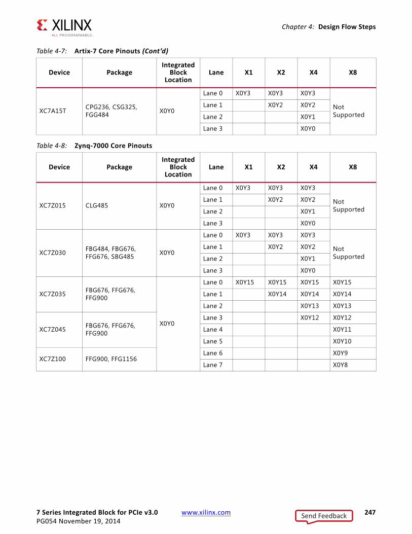
7 Series Integrated Block for PCIe v3.0 www.xilinx.com 247PG054 November 19, 2014
Chapter 4: Design Flow Steps
XC7A15T CPG236, CSG325, FGG484 X0Y0
Lane 0 X0Y3 X0Y3 X0Y3
Not Supported
Lane 1 X0Y2 X0Y2
Lane 2 X0Y1
Lane 3 X0Y0
Table 4-8: Zynq-7000 Core Pinouts
Device PackageIntegrated
Block Location
Lane X1 X2 X4 X8
XC7Z015 CLG485 X0Y0
Lane 0 X0Y3 X0Y3 X0Y3
Not Supported
Lane 1 X0Y2 X0Y2
Lane 2 X0Y1
Lane 3 X0Y0
XC7Z030 FBG484, FBG676, FFG676, SBG485 X0Y0
Lane 0 X0Y3 X0Y3 X0Y3
Not Supported
Lane 1 X0Y2 X0Y2
Lane 2 X0Y1
Lane 3 X0Y0
XC7Z035 FBG676, FFG676, FFG900
X0Y0
Lane 0 X0Y15 X0Y15 X0Y15 X0Y15
Lane 1 X0Y14 X0Y14 X0Y14
Lane 2 X0Y13 X0Y13
XC7Z045 FBG676, FFG676, FFG900
Lane 3 X0Y12 X0Y12
Lane 4 X0Y11
Lane 5 X0Y10
XC7Z100 FFG900, FFG1156Lane 6 X0Y9
Lane 7 X0Y8
Table 4-7: Artix-7 Core Pinouts (Cont’d)
Device PackageIntegrated
Block Location
Lane X1 X2 X4 X8
Send Feedback
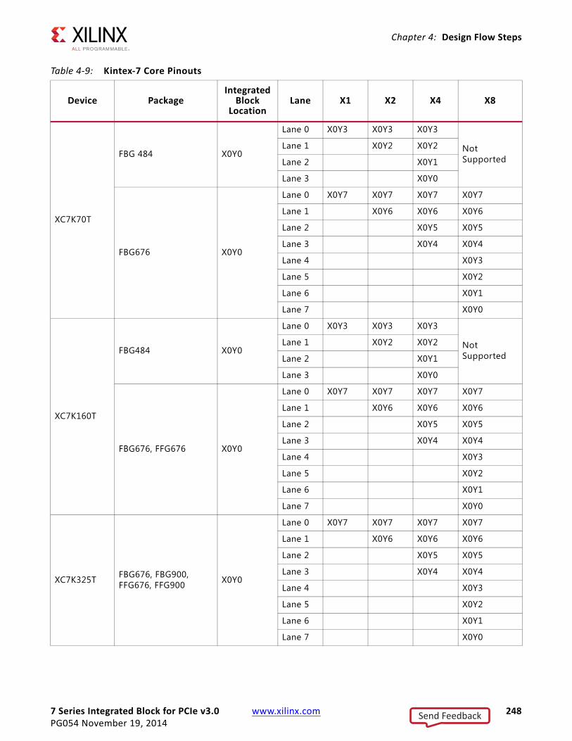
7 Series Integrated Block for PCIe v3.0 www.xilinx.com 248PG054 November 19, 2014
Chapter 4: Design Flow Steps
Table 4-9: Kintex-7 Core Pinouts
Device PackageIntegrated
Block Location
Lane X1 X2 X4 X8
XC7K70T
FBG 484 X0Y0
Lane 0 X0Y3 X0Y3 X0Y3
Not Supported
Lane 1 X0Y2 X0Y2
Lane 2 X0Y1
Lane 3 X0Y0
FBG676 X0Y0
Lane 0 X0Y7 X0Y7 X0Y7 X0Y7
Lane 1 X0Y6 X0Y6 X0Y6
Lane 2 X0Y5 X0Y5
Lane 3 X0Y4 X0Y4
Lane 4 X0Y3
Lane 5 X0Y2
Lane 6 X0Y1
Lane 7 X0Y0
XC7K160T
FBG484 X0Y0
Lane 0 X0Y3 X0Y3 X0Y3
Not Supported
Lane 1 X0Y2 X0Y2
Lane 2 X0Y1
Lane 3 X0Y0
FBG676, FFG676 X0Y0
Lane 0 X0Y7 X0Y7 X0Y7 X0Y7
Lane 1 X0Y6 X0Y6 X0Y6
Lane 2 X0Y5 X0Y5
Lane 3 X0Y4 X0Y4
Lane 4 X0Y3
Lane 5 X0Y2
Lane 6 X0Y1
Lane 7 X0Y0
XC7K325T FBG676, FBG900, FFG676, FFG900 X0Y0
Lane 0 X0Y7 X0Y7 X0Y7 X0Y7
Lane 1 X0Y6 X0Y6 X0Y6
Lane 2 X0Y5 X0Y5
Lane 3 X0Y4 X0Y4
Lane 4 X0Y3
Lane 5 X0Y2
Lane 6 X0Y1
Lane 7 X0Y0
Send Feedback
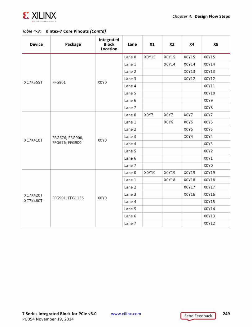
7 Series Integrated Block for PCIe v3.0 www.xilinx.com 249PG054 November 19, 2014
Chapter 4: Design Flow Steps
XC7K355T FFG901 X0Y0
Lane 0 X0Y15 X0Y15 X0Y15 X0Y15
Lane 1 X0Y14 X0Y14 X0Y14
Lane 2 X0Y13 X0Y13
Lane 3 X0Y12 X0Y12
Lane 4 X0Y11
Lane 5 X0Y10
Lane 6 X0Y9
Lane 7 X0Y8
XC7K410T FBG676, FBG900, FFG676, FFG900 X0Y0
Lane 0 X0Y7 X0Y7 X0Y7 X0Y7
Lane 1 X0Y6 X0Y6 X0Y6
Lane 2 X0Y5 X0Y5
Lane 3 X0Y4 X0Y4
Lane 4 X0Y3
Lane 5 X0Y2
Lane 6 X0Y1
Lane 7 X0Y0
XC7K420TXC7K480T
FFG901, FFG1156 X0Y0
Lane 0 X0Y19 X0Y19 X0Y19 X0Y19
Lane 1 X0Y18 X0Y18 X0Y18
Lane 2 X0Y17 X0Y17
Lane 3 X0Y16 X0Y16
Lane 4 X0Y15
Lane 5 X0Y14
Lane 6 X0Y13
Lane 7 X0Y12
Table 4-9: Kintex-7 Core Pinouts (Cont’d)
Device PackageIntegrated
Block Location
Lane X1 X2 X4 X8
Send Feedback
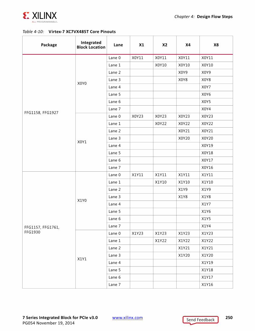
7 Series Integrated Block for PCIe v3.0 www.xilinx.com 250PG054 November 19, 2014
Chapter 4: Design Flow Steps
Table 4-10: Virtex-7 XC7VX485T Core Pinouts
Package Integrated Block Location Lane X1 X2 X4 X8
FFG1158, FFG1927
X0Y0
Lane 0 X0Y11 X0Y11 X0Y11 X0Y11
Lane 1 X0Y10 X0Y10 X0Y10
Lane 2 X0Y9 X0Y9
Lane 3 X0Y8 X0Y8
Lane 4 X0Y7
Lane 5 X0Y6
Lane 6 X0Y5
Lane 7 X0Y4
X0Y1
Lane 0 X0Y23 X0Y23 X0Y23 X0Y23
Lane 1 X0Y22 X0Y22 X0Y22
Lane 2 X0Y21 X0Y21
Lane 3 X0Y20 X0Y20
Lane 4 X0Y19
Lane 5 X0Y18
Lane 6 X0Y17
Lane 7 X0Y16
FFG1157, FFG1761, FFG1930
X1Y0
Lane 0 X1Y11 X1Y11 X1Y11 X1Y11
Lane 1 X1Y10 X1Y10 X1Y10
Lane 2 X1Y9 X1Y9
Lane 3 X1Y8 X1Y8
Lane 4 X1Y7
Lane 5 X1Y6
Lane 6 X1Y5
Lane 7 X1Y4
X1Y1
Lane 0 X1Y23 X1Y23 X1Y23 X1Y23
Lane 1 X1Y22 X1Y22 X1Y22
Lane 2 X1Y21 X1Y21
Lane 3 X1Y20 X1Y20
Lane 4 X1Y19
Lane 5 X1Y18
Lane 6 X1Y17
Lane 7 X1Y16
Send Feedback
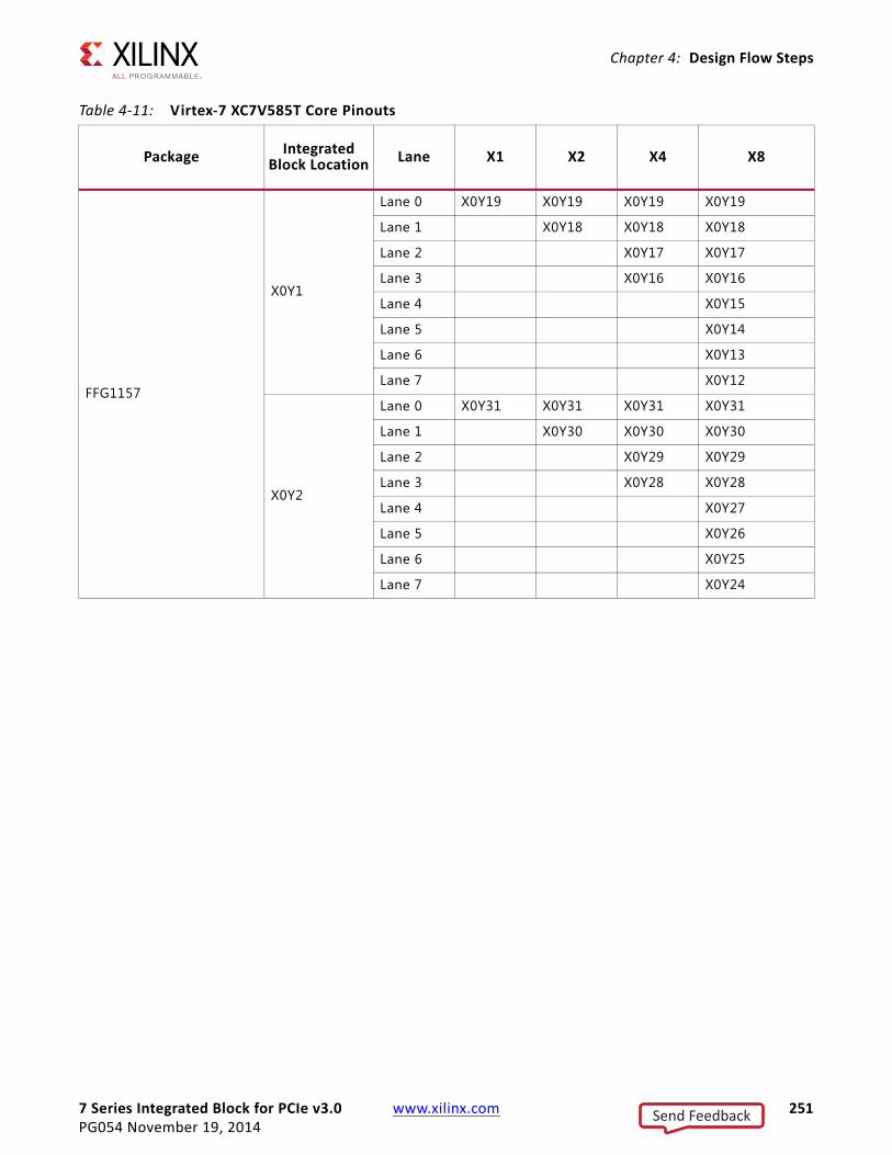
7 Series Integrated Block for PCIe v3.0 www.xilinx.com 251PG054 November 19, 2014
Chapter 4: Design Flow Steps
Table 4-11: Virtex-7 XC7V585T Core Pinouts
Package Integrated Block Location Lane X1 X2 X4 X8
FFG1157
X0Y1
Lane 0 X0Y19 X0Y19 X0Y19 X0Y19
Lane 1 X0Y18 X0Y18 X0Y18
Lane 2 X0Y17 X0Y17
Lane 3 X0Y16 X0Y16
Lane 4 X0Y15
Lane 5 X0Y14
Lane 6 X0Y13
Lane 7 X0Y12
X0Y2
Lane 0 X0Y31 X0Y31 X0Y31 X0Y31
Lane 1 X0Y30 X0Y30 X0Y30
Lane 2 X0Y29 X0Y29
Lane 3 X0Y28 X0Y28
Lane 4 X0Y27
Lane 5 X0Y26
Lane 6 X0Y25
Lane 7 X0Y24
Send Feedback
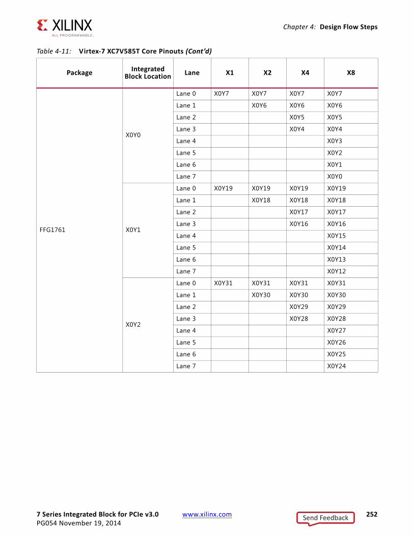
7 Series Integrated Block for PCIe v3.0 www.xilinx.com 252PG054 November 19, 2014
Chapter 4: Design Flow Steps
FFG1761
X0Y0
Lane 0 X0Y7 X0Y7 X0Y7 X0Y7
Lane 1 X0Y6 X0Y6 X0Y6
Lane 2 X0Y5 X0Y5
Lane 3 X0Y4 X0Y4
Lane 4 X0Y3
Lane 5 X0Y2
Lane 6 X0Y1
Lane 7 X0Y0
X0Y1
Lane 0 X0Y19 X0Y19 X0Y19 X0Y19
Lane 1 X0Y18 X0Y18 X0Y18
Lane 2 X0Y17 X0Y17
Lane 3 X0Y16 X0Y16
Lane 4 X0Y15
Lane 5 X0Y14
Lane 6 X0Y13
Lane 7 X0Y12
X0Y2
Lane 0 X0Y31 X0Y31 X0Y31 X0Y31
Lane 1 X0Y30 X0Y30 X0Y30
Lane 2 X0Y29 X0Y29
Lane 3 X0Y28 X0Y28
Lane 4 X0Y27
Lane 5 X0Y26
Lane 6 X0Y25
Lane 7 X0Y24
Table 4-11: Virtex-7 XC7V585T Core Pinouts (Cont’d)
Package Integrated Block Location Lane X1 X2 X4 X8
Send Feedback
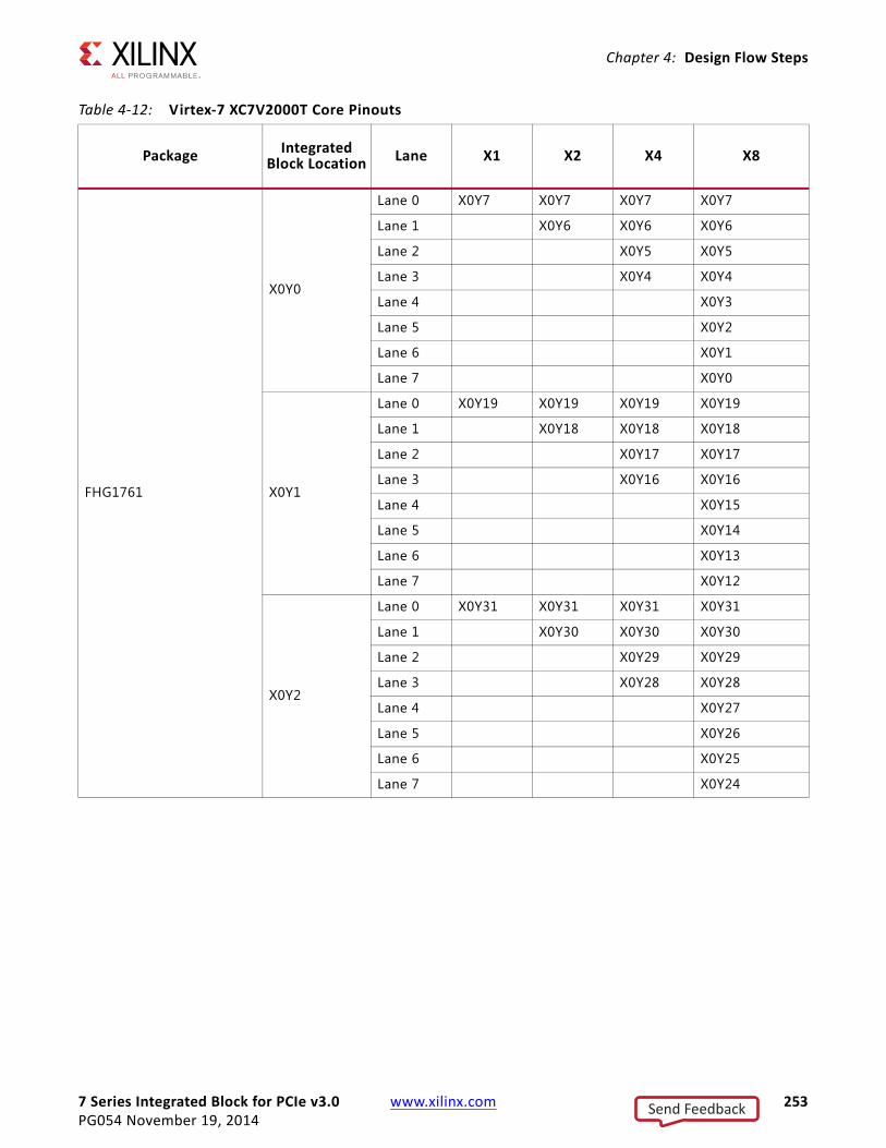
7 Series Integrated Block for PCIe v3.0 www.xilinx.com 253PG054 November 19, 2014
Chapter 4: Design Flow Steps
Table 4-12: Virtex-7 XC7V2000T Core Pinouts
Package Integrated Block Location Lane X1 X2 X4 X8
FHG1761
X0Y0
Lane 0 X0Y7 X0Y7 X0Y7 X0Y7
Lane 1 X0Y6 X0Y6 X0Y6
Lane 2 X0Y5 X0Y5
Lane 3 X0Y4 X0Y4
Lane 4 X0Y3
Lane 5 X0Y2
Lane 6 X0Y1
Lane 7 X0Y0
X0Y1
Lane 0 X0Y19 X0Y19 X0Y19 X0Y19
Lane 1 X0Y18 X0Y18 X0Y18
Lane 2 X0Y17 X0Y17
Lane 3 X0Y16 X0Y16
Lane 4 X0Y15
Lane 5 X0Y14
Lane 6 X0Y13
Lane 7 X0Y12
X0Y2
Lane 0 X0Y31 X0Y31 X0Y31 X0Y31
Lane 1 X0Y30 X0Y30 X0Y30
Lane 2 X0Y29 X0Y29
Lane 3 X0Y28 X0Y28
Lane 4 X0Y27
Lane 5 X0Y26
Lane 6 X0Y25
Lane 7 X0Y24
Send Feedback

7 Series Integrated Block for PCIe v3.0 www.xilinx.com 254PG054 November 19, 2014
Chapter 4: Design Flow Steps
SimulationThis section contains information about simulating IP in the Vivado Design Suite.
• For comprehensive information about Vivado simulation components, as well as information about using supported third party tools, see the Vivado Design Suite User Guide: Logic Simulation (UG900) [Ref 15].
• For information about simulating the example design, see Simulating the Example Design in Chapter 5.
Simulating with Tandem ConfigurationsFor specif ic requirements for simulating with Tandem Configurations, see Simulating the Tandem IP Core in Chapter 3.
FLG1925
X0Y0
Lane 0 X0Y11 X0Y11 X0Y11 X0Y11
Lane 1 X0Y10 X0Y10 X0Y10
Lane 2 X0Y9 X0Y9
Lane 3 X0Y8 X0Y8
Lane 4 X0Y7
Lane 5 X0Y6
Lane 6 X0Y5
Lane 7 X0Y4
X0Y1
Lane 0 X0Y19 X0Y19 X0Y19 X0Y19
Lane 1 X0Y18 X0Y18 X0Y18
Lane 2 X0Y17 X0Y17
Lane 3 X0Y16 X0Y16
Lane 4 X0Y15
Lane 5 X0Y14
Lane 6 X0Y13
Lane 7 X0Y12
Table 4-12: Virtex-7 XC7V2000T Core Pinouts (Cont’d)
Package Integrated Block Location Lane X1 X2 X4 X8
Send Feedback
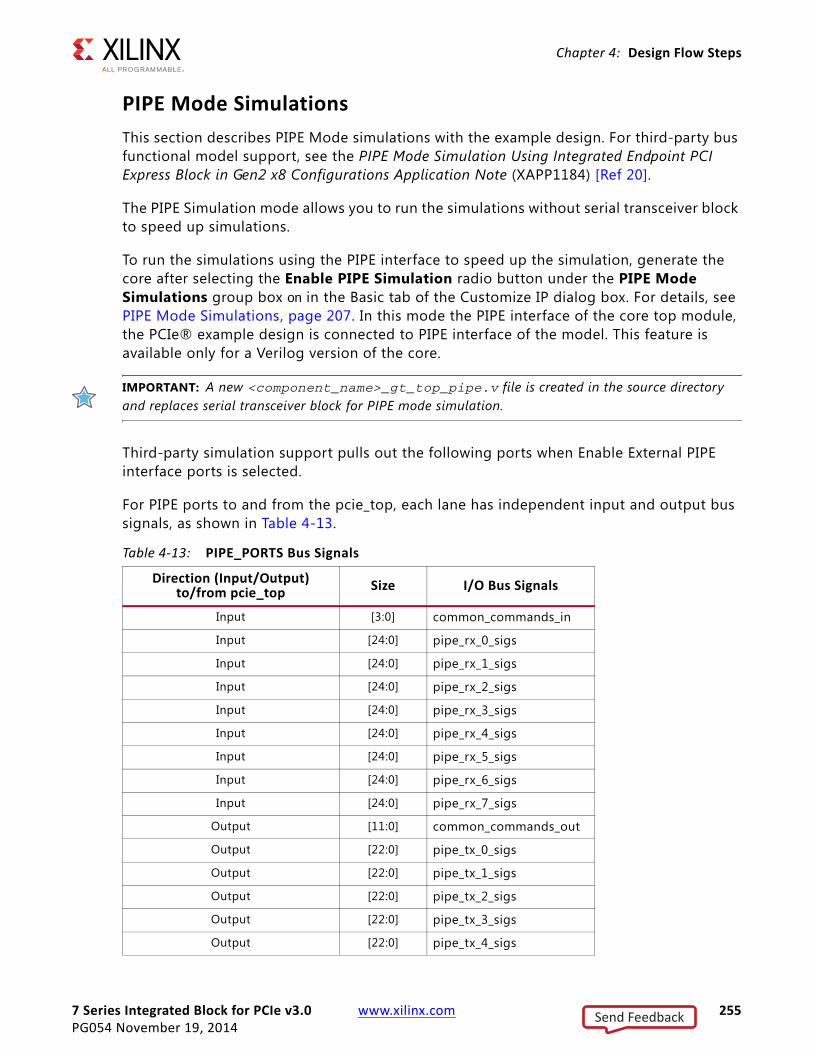
7 Series Integrated Block for PCIe v3.0 www.xilinx.com 255PG054 November 19, 2014
Chapter 4: Design Flow Steps
PIPE Mode SimulationsThis section describes PIPE Mode simulations with the example design. For third-party bus functional model support, see the PIPE Mode Simulation Using Integrated Endpoint PCI Express Block in Gen2 x8 Configurations Application Note (XAPP1184) [Ref 20].
The PIPE Simulation mode allows you to run the simulations without serial transceiver block to speed up simulations.
To run the simulations using the PIPE interface to speed up the simulation, generate the core after selecting the Enable PIPE Simulation radio button under the PIPE Mode Simulations group box on in the Basic tab of the Customize IP dialog box. For details, see PIPE Mode Simulations, page 207. In this mode the PIPE interface of the core top module, the PCIe® example design is connected to PIPE interface of the model. This feature is available only for a Verilog version of the core.
IMPORTANT: A new <component_name>_gt_top_pipe.v file is created in the source directory and replaces serial transceiver block for PIPE mode simulation.
Third-party simulation support pulls out the following ports when Enable External PIPE interface ports is selected.
For PIPE ports to and from the pcie_top, each lane has independent input and output bus signals, as shown in Table 4-13.
Table 4-13: PIPE_PORTS Bus Signals
Direction (Input/Output)to/from pcie_top Size I/O Bus Signals
Input [3:0] common_commands_in
Input [24:0] pipe_rx_0_sigs
Input [24:0] pipe_rx_1_sigs
Input [24:0] pipe_rx_2_sigs
Input [24:0] pipe_rx_3_sigs
Input [24:0] pipe_rx_4_sigs
Input [24:0] pipe_rx_5_sigs
Input [24:0] pipe_rx_6_sigs
Input [24:0] pipe_rx_7_sigs
Output [11:0] common_commands_out
Output [22:0] pipe_tx_0_sigs
Output [22:0] pipe_tx_1_sigs
Output [22:0] pipe_tx_2_sigs
Output [22:0] pipe_tx_3_sigs
Output [22:0] pipe_tx_4_sigs
Send Feedback
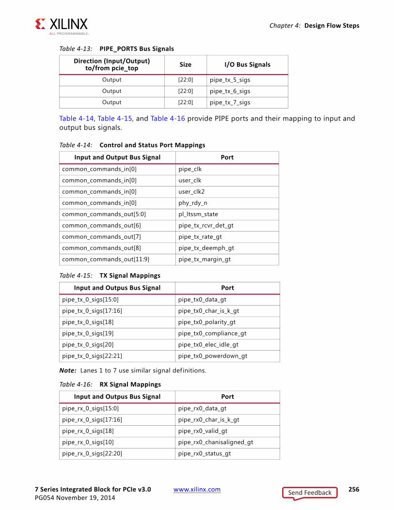
7 Series Integrated Block for PCIe v3.0 www.xilinx.com 256PG054 November 19, 2014
Chapter 4: Design Flow Steps
Table 4-14, Table 4-15, and Table 4-16 provide PIPE ports and their mapping to input and output bus signals.
Note: Lanes 1 to 7 use similar signal definitions.
Output [22:0] pipe_tx_5_sigs
Output [22:0] pipe_tx_6_sigs
Output [22:0] pipe_tx_7_sigs
Table 4-14: Control and Status Port Mappings
Input and Output Bus Signal Port
common_commands_in[0] pipe_clk
common_commands_in[0] user_clk
common_commands_in[0] user_clk2
common_commands_in[0] phy_rdy_n
common_commands_out[5:0] pl_ltssm_state
common_commands_out[6] pipe_tx_rcvr_det_gt
common_commands_out[7] pipe_tx_rate_gt
common_commands_out[8] pipe_tx_deemph_gt
common_commands_out[11:9] pipe_tx_margin_gt
Table 4-15: TX Signal Mappings
Input and Outpus Bus Signal Port
pipe_tx_0_sigs[15:0] pipe_tx0_data_gt
pipe_tx_0_sigs[17:16] pipe_tx0_char_is_k_gt
pipe_tx_0_sigs[18] pipe_tx0_polarity_gt
pipe_tx_0_sigs[19] pipe_tx0_compliance_gt
pipe_tx_0_sigs[20] pipe_tx0_elec_idle_gt
pipe_tx_0_sigs[22:21] pipe_tx0_powerdown_gt
Table 4-16: RX Signal Mappings
Input and Outpus Bus Signal Port
pipe_rx_0_sigs[15:0] pipe_rx0_data_gt
pipe_rx_0_sigs[17:16] pipe_rx0_char_is_k_gt
pipe_rx_0_sigs[18] pipe_rx0_valid_gt
pipe_rx_0_sigs[10] pipe_rx0_chanisaligned_gt
pipe_rx_0_sigs[22:20] pipe_rx0_status_gt
Table 4-13: PIPE_PORTS Bus Signals
Direction (Input/Output)to/from pcie_top Size I/O Bus Signals
Send Feedback

7 Series Integrated Block for PCIe v3.0 www.xilinx.com 257PG054 November 19, 2014
Chapter 4: Design Flow Steps
Note: Lanes 1 to 7 use similar signal definitions.
Synthesis and Implementation• For further details about synthesis and implementation, see the Vivado Design Suite
User Guide: Designing with IP (UG896) [Ref 14].
• For information regarding synthesizing and implementing the example design, see Synthesizing and Implementing the Example Design in Chapter 5.
pipe_rx_0_sigs[23] pipe_rx0_phy_status_gt
pipe_rx_0_sigs[24] pipe_rx0_elec_idle_gt
Table 4-16: RX Signal Mappings
Input and Outpus Bus Signal Port
Send Feedback
7 Series Integrated Block for PCIe v3.0 www.xilinx.com 258PG054 November 19, 2014
Chapter 5
Detailed Example DesignsThis section provides an overview of the 7 Series FPGAs Integrated Block for PCI Express® example designs, and instructions for generating the core.
Integrated Block Endpoint Configuration OverviewThe example simulation design for the Endpoint configuration of the integrated block consists of two discrete parts:
• The Root Port Model: A test bench that generates, consumes, and checks PCI Express bus traff ic.
• The Programmed Input/Output (PIO) example design: A completer application for PCI Express. The PIO example design responds to Read and Write requests to its memory space and can be synthesized for testing in hardware.
Simulation Design OverviewFor the simulation design, transactions are sent from the Root Port Model to the core (configured as an Endpoint) and processed by the PIO example design. Figure 5-1 illustrates the simulation design provided with the Integrated Block core. For more information about the Root Port Model, see Root Port Model Test Bench for Endpoint in Chapter 6.
Send Feedback
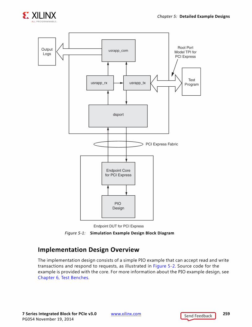
7 Series Integrated Block for PCIe v3.0 www.xilinx.com 259PG054 November 19, 2014
Chapter 5: Detailed Example Designs
Implementation Design OverviewThe implementation design consists of a simple PIO example that can accept read and write transactions and respond to requests, as illustrated in Figure 5-2. Source code for the example is provided with the core. For more information about the PIO example design, see Chapter 6, Test Benches.
X-Ref Target - Figure 5-1
Figure 5-1: Simulation Example Design Block Diagram
dsport
PCI Express Fabric
Endpoint Corefor PCI Express
PIO Design
usrapp_txusrapp_rx
Endpoint DUT for PCI Express
usrapp_comOutputLogs
TestProgram
Root PortModel TPI forPCI Express
Send Feedback
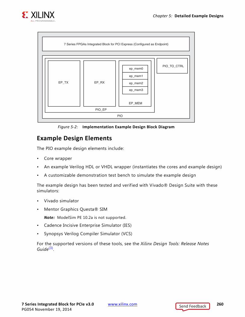
7 Series Integrated Block for PCIe v3.0 www.xilinx.com 260PG054 November 19, 2014
Chapter 5: Detailed Example Designs
Example Design ElementsThe PIO example design elements include:
• Core wrapper
• An example Verilog HDL or VHDL wrapper (instantiates the cores and example design)
• A customizable demonstration test bench to simulate the example design
The example design has been tested and verif ied with Vivado® Design Suite with these simulators:
• Vivado simulator
• Mentor Graphics Questa® SIM
Note: ModelSim PE 10.2a is not supported.
• Cadence Incisive Enterprise Simulator (IES)
• Synopsys Verilog Compiler Simulator (VCS)
For the supported versions of these tools, see the Xilinx Design Tools: Release Notes Guide(3).
X-Ref Target - Figure 5-2
Figure 5-2: Implementation Example Design Block Diagram
7 Series FPGAs Integrated Block for PCI Express (Configured as Endpoint)
EP_TX EP_RX
ep_mem0
ep_mem1
ep_mem2
ep_mem3
EP_MEM
PIO_EP
PIO
PIO_TO_CTRL
Send Feedback
7 Series Integrated Block for PCIe v3.0 www.xilinx.com 261PG054 November 19, 2014
Chapter 5: Detailed Example Designs
Programmed Input/Output: Endpoint Example DesignProgrammed Input/Output (PIO) transactions are generally used by a PCI Express® system host CPU to access Memory Mapped Input/Output (MMIO) and Configuration Mapped Input/Output (CMIO) locations in the PCI Express logic. Endpoints for PCI Express accept Memory and I/O Write transactions and respond to Memory and I/O Read transactions with Completion with Data transactions.
The PIO example design (PIO design) is included with the core in an Endpoint configuration generated by the Vivado Integrated Design Environment (IDE).
TIP: You can bring up the system board and verify the link and functionality of the board using the PIO design, which is an established working design.
Note: The PIO design Port Model is shared by the 7 Series FPGAs Integrated Block for PCI Express, Endpoint Block Plus for PCI Express, and Endpoint PIPE for PCI Express solutions. This chapter represents all the solutions generically using the name Endpoint for PCI Express (or Endpoint for PCIe®).
System OverviewThe PIO design is a simple target-only application that interfaces with the Endpoint for PCIe core Transaction (AXI4-Stream) interface and is provided as a starting point for building your own designs. These features are included:
• Four transaction-specif ic 2 KB target regions using the internal Xilinx FPGA block RAMs, providing a total target space of 8192 bytes
• Supports single DWORD payload Read and Write PCI Express transactions to 32-/64-bit address memory spaces and I/O space with support for completion TLPs
• Utilizes the (rx_bar_hit[7:0]) m_axis_rx_tuser[9:2] signals of the core to differentiate between TLP destination Base Address Registers
• Provides separate implementations optimized for 32-bit, 64-bit, and 128-bit AXI4-Stream interfaces
Figure 5-3 illustrates the PCI Express system architecture components, consisting of a Root Complex, a PCI Express switch device, and an Endpoint for PCIe. PIO operations move data downstream from the Root Complex (CPU register) to the Endpoint, and/or upstream from the Endpoint to the Root Complex (CPU register). In either case, the PCI Express protocol request to move the data is initiated by the host CPU.
Send Feedback
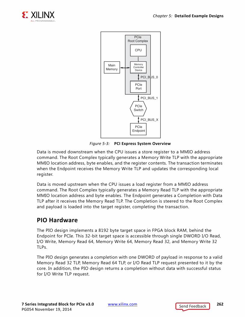
7 Series Integrated Block for PCIe v3.0 www.xilinx.com 262PG054 November 19, 2014
Chapter 5: Detailed Example Designs
Data is moved downstream when the CPU issues a store register to a MMIO address command. The Root Complex typically generates a Memory Write TLP with the appropriate MMIO location address, byte enables, and the register contents. The transaction terminates when the Endpoint receives the Memory Write TLP and updates the corresponding local register.
Data is moved upstream when the CPU issues a load register from a MMIO address command. The Root Complex typically generates a Memory Read TLP with the appropriate MMIO location address and byte enables. The Endpoint generates a Completion with Data TLP after it receives the Memory Read TLP. The Completion is steered to the Root Complex and payload is loaded into the target register, completing the transaction.
PIO HardwareThe PIO design implements a 8192 byte target space in FPGA block RAM, behind the Endpoint for PCIe. This 32-bit target space is accessible through single DWORD I/O Read, I/O Write, Memory Read 64, Memory Write 64, Memory Read 32, and Memory Write 32 TLPs.
The PIO design generates a completion with one DWORD of payload in response to a valid Memory Read 32 TLP, Memory Read 64 TLP, or I/O Read TLP request presented to it by the core. In addition, the PIO design returns a completion without data with successful status for I/O Write TLP request.
X-Ref Target - Figure 5-3
Figure 5-3: PCI Express System Overview
MainMemory
PCI_BUS_X
PCI_BUS_1
PCI_BUS_0
CPU
MemoryController
Device
PCIePort
PCIeSwitch
PCIeEndpoint
PCIeRoot Complex
Send Feedback
7 Series Integrated Block for PCIe v3.0 www.xilinx.com 263PG054 November 19, 2014
Chapter 5: Detailed Example Designs
The PIO design processes a Memory or I/O Write TLP with one DWORD payload by updating the payload into the target address in the FPGA block RAM space.
Base Address Register SupportThe PIO design supports four discrete target spaces, each consisting of a 2 KB block of memory represented by a separate Base Address Register (BAR). Using the default parameters, the Vivado IDE produces a core configured to work with the PIO design that consists of:
• One 64-bit addressable Memory Space BAR
• One 32-bit Addressable Memory Space BAR
You can change the default parameters used by the PIO design; however, in some cases you might need to change the user application depending on your system. See Changing the Default BAR Settings for information about changing the default parameters and the effect on the PIO design.
Each of the four 2 KB address spaces represented by the BARs corresponds to one of four 2 KB address regions in the PIO design. Each 2 KB region is implemented using a 2 KB dual-port block RAM. As transactions are received by the core, the core decodes the address and determines which of the four regions is being targeted. The core presents the TLP to the PIO design and asserts the appropriate bits of (rx_bar_hit[7:0]) m_axis_rx_tuser[9:2], as defined in Table 5-1.
Changing the Default BAR Settings
You can change the parameters and continue to use the PIO design to create customized Verilog or VHDL source to match the selected BAR settings. However, because the PIO design parameters are more limited than the core parameters, consider these example design limitations when changing the default parameters:
• The example design supports one I/O space BAR, one 32-bit Memory space (that cannot be the Expansion ROM space), and one 64-bit Memory space. If these limits are exceeded, only the f irst space of a given type is active—accesses to the other spaces do not result in completions.
Table 5-1: TLP Traffic Types
Block RAM TLP Transaction Type Default BAR rx_bar_hit[7:0]
ep_mem0 I/O TLP transactions Disabled Disabled
ep_mem1 32-bit address Memory TLP transactions 0 0000_0001b
ep_mem2 64-bit address Memory TLP transactions Disabled Disabled
ep_mem3 32-bit address Memory TLP transactions destined for EROM
Expansion ROM 0100_0000b
Send Feedback

7 Series Integrated Block for PCIe v3.0 www.xilinx.com 264PG054 November 19, 2014
Chapter 5: Detailed Example Designs
• Each space is implemented with a 2 KB memory. If the corresponding BAR is configured to a wider aperture, accesses beyond the 2 KB limit wrap around and overlap the 2 KB memory space.
• The PIO design supports one I/O space BAR, which by default is disabled, but can be changed if desired.
TIP: Although there are limitations to the PIO design, Verilog or VHDL source code is provided so you can tailor the example design to your specific needs.
TLP Data Flow
This section defines the data flow of a TLP successfully processed by the PIO design. For detailed information about the interface signals within the sub-blocks of the PIO design, see Receive Path, page 268 and Transmit Path, page 269.
The PIO design successfully processes single DWORD payload Memory Read and Write TLPs and I/O Read and Write TLPs. Memory Read or Memory Write TLPs of lengths larger than one DWORD are not processed correctly by the PIO design; however, the core does accept these TLPs and passes them along to the PIO design. If the PIO design receives a TLP with a length of greater than one DWORD, the TLP is received completely from the core and discarded. No corresponding completion is generated.
Memory and I/O Write TLP Processing
When the Endpoint for PCIe receives a Memory or I/O Write TLP, the TLP destination address and transaction type are compared with the values in the core BARs. If the TLP passes this comparison check, the core passes the TLP to the Receive AXI4-Stream interface of the PIO design. The PIO design handles Memory writes and I/O TLP writes in different ways: the PIO design responds to I/O writes by generating a Completion Without Data (cpl), a requirement of the PCI Express specif ication.
Along with the start of packet, end of packet, and ready handshaking signals, the Receive AXI4-Stream interface also asserts the appropriate (rx_bar_hit[7:0]) m_axis_rx_tuser[9:2] signal to indicate to the PIO design the specific destination BAR that matched the incoming TLP. On reception, the RX State Machine of the PIO design processes the incoming Write TLP and extracts the TLPs data and relevant address fields so that it can pass this along to the internal block RAM write request controller of the PIO design.
Based on the specif ic rx_bar_hit[7:0] signal asserted, the RX State Machine indicates to the internal write controller the appropriate 2 KB block RAM to use prior to asserting the write enable request. For example, if an Memory Write 32 Request is received by the core targeting BAR0, the core passes the TLP to the PIO design and asserts rx_bar_hit[0]. The RX State machine extracts the lower address bits and the data f ield from the Memory Write 32 Request TLP and instructs the internal Memory Write controller to begin a write to the block RAM.
Send Feedback
7 Series Integrated Block for PCIe v3.0 www.xilinx.com 265PG054 November 19, 2014
Chapter 5: Detailed Example Designs
In this example, the assertion of rx_bar_hit[0] instructed the PIO memory write controller to access ep_mem1 (which by default represents 2 KB of Mem32 space). While the write is being carried out to the FPGA block RAM, the PIO design RX state machine deasserts the m_axis_rx_tready, causing the Receive AXI4-Stream interface to stall receiving any further TLPs until the internal Memory Write controller completes the write to the block RAM. Deasserting m_axis_rx_tready in this way is not required for all designs using the core—the PIO design uses this method to simplify the control logic of the RX state machine.
Memory and I/O Read TLP Processing
When the Endpoint for PCIe receives a Memory or I/O Read TLP, the TLP destination address and transaction type are compared with the values programmed in the core BARs. If the TLP passes this comparison check, the core passes the TLP to the Receive AXI4-Stream interface of the PIO design.
Along with the start of packet, end of packet, and ready handshaking signals, the Receive AXI4-Stream interface also asserts the appropriate rx_bar_hit[7:0] signal to indicate to the PIO design the specific destination BAR that matched the incoming TLP. On reception, the state machine of the PIO design processes the incoming Read TLP and extracts the relevant TLP information and passes it along to the internal block RAM read request controller of the PIO design.
Based on the specif ic rx_bar_hit[7:0] signal asserted, the RX state machine indicates to the internal read request controller the appropriate 2 KB block RAM to use before asserting the read enable request. For example, if a Memory Read 32 Request TLP is received by the core targeting the default MEM32 BAR2, the core passes the TLP to the PIO design and asserts rx_bar_hit[0]. The RX State machine extracts the lower address bits from the Memory 32 Read TLP and instructs the internal Memory Read Request controller to start a read operation.
In this example, the assertion of rx_bar_hit[0] instructs the PIO memory read controller to access the Mem32 space, which by default represents 2 KB of memory space. A notable difference in handling of memory write and read TLPs is the requirement of the receiving device to return a Completion with Data TLP in the case of memory or I/O read request.
While the read is being processed, the PIO design RX state machine deasserts m_axis_rx_tready, causing the Receive AXI4-Stream interface to stall receiving any further TLPs until the internal Memory Read controller completes the read access from the block RAM and generates the completion. Deasserting m_axis_rx_tready in this way is not required for all designs using the core. The PIO design uses this method to simplify the control logic of the RX state machine.
PIO File Structure
Table 5-2 defines the PIO design file structure. Based on the specif ic core targeted, not all f iles delivered by the Vivado IDE are necessary, and some files might not be delivered. The major difference is that some of the Endpoint for PCIe solutions use a 64-bit user datapath,
Send Feedback
7 Series Integrated Block for PCIe v3.0 www.xilinx.com 266PG054 November 19, 2014
Chapter 5: Detailed Example Designs
while others use a 128-bit datapath, and the PIO design works with both. The width of the datapath depends on the specif ic core being targeted.
Three configurations of the PIO design are provided: PIO_64, and PIO_128 with 64-, and 128-bit AXI4-Stream interfaces, respectively. The PIO configuration generated depends on the selected Endpoint type (that is, 7 series FPGAs Integrated Block) as well as the number of PCI Express lanes and the interface width you selected. Table 5-3 identif ies the PIO configuration generated based on your selection.
Figure 5-4 shows the various components of the PIO design, which is separated into four main parts: the TX Engine, RX Engine, Memory Access Controller, and Power Management Turn-Off Controller.
Table 5-2: PIO Design File Structure
File Description
pcie_app_7vx.v Top-level design wrapper
PIO.v PIO design wrapper
PIO_EP.v PIO application module
PIO_TO_CTRL.v PIO turn-off controller module
PIO_RX_ENGINE.v 64-bit/128-bit Receive engine
PIO_TX_ENGINE.v 64-bit/128-bit Transmit engine
PIO_EP_MEM_ACCESS.v Endpoint memory access module
PIO_EP_MEM.v Endpoint memory
Table 5-3: PIO Configuration
Core x1 x2 x4 x8
7 Series FPGAs Integrated Block PIO_64 PIO_64 PIO_64, PIO_128
PIO_64, PIO_128
Send Feedback
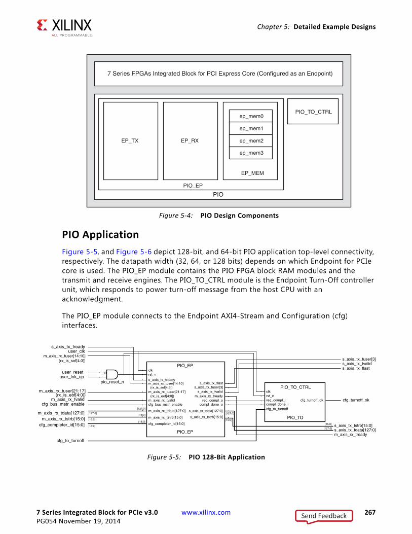
7 Series Integrated Block for PCIe v3.0 www.xilinx.com 267PG054 November 19, 2014
Chapter 5: Detailed Example Designs
PIO ApplicationFigure 5-5, and Figure 5-6 depict 128-bit, and 64-bit PIO application top-level connectivity, respectively. The datapath width (32, 64, or 128 bits) depends on which Endpoint for PCIe core is used. The PIO_EP module contains the PIO FPGA block RAM modules and the transmit and receive engines. The PIO_TO_CTRL module is the Endpoint Turn-Off controller unit, which responds to power turn-off message from the host CPU with an acknowledgment.
The PIO_EP module connects to the Endpoint AXI4-Stream and Configuration (cfg) interfaces.
X-Ref Target - Figure 5-4
Figure 5-4: PIO Design Components
7 Series FPGAs Integrated Block for PCI Express Core (Configured as an Endpoint)
PIO
PIO_TO_CTRL
PIO_EP
EP_TX EP_RX
EP_MEM
ep_mem0
ep_mem1
ep_mem2
ep_mem3
X-Ref Target - Figure 5-5
Figure 5-5: PIO 128-Bit Application
Send Feedback
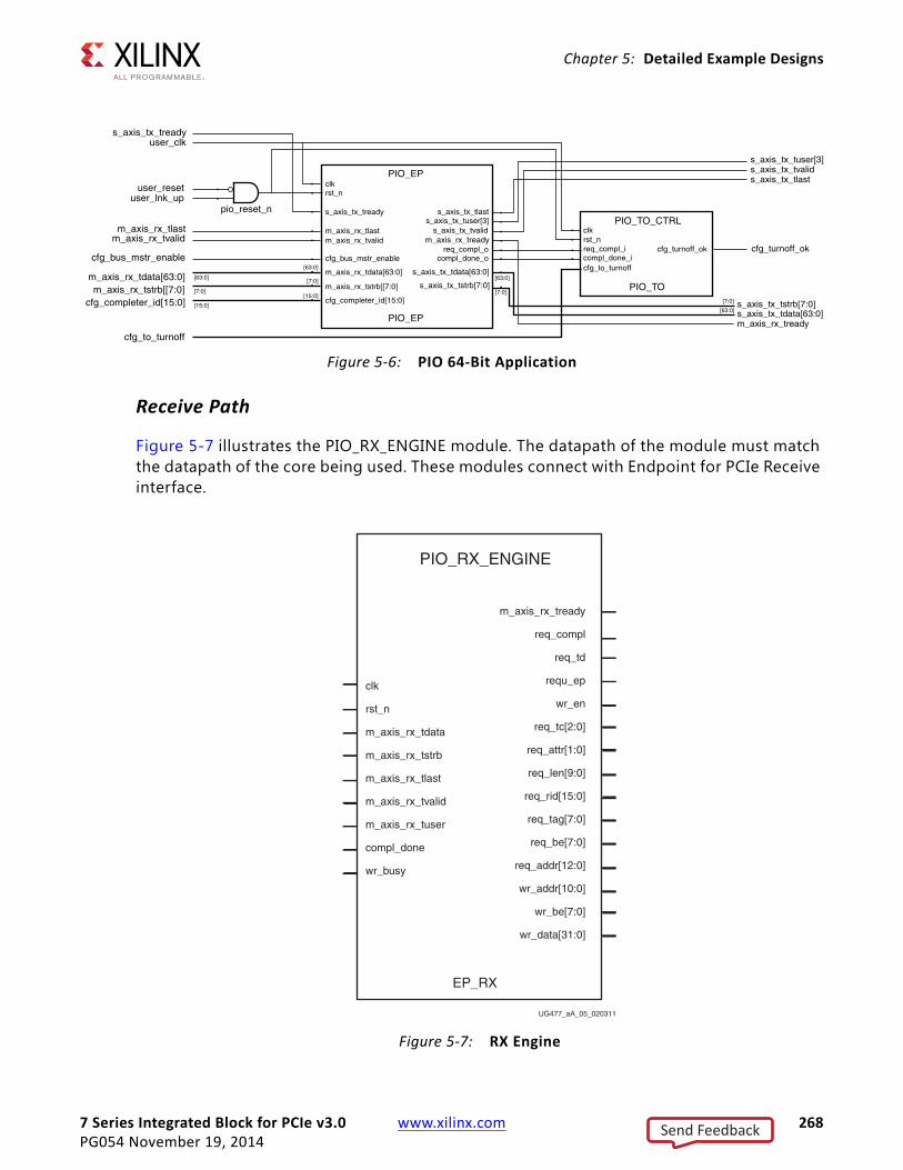
7 Series Integrated Block for PCIe v3.0 www.xilinx.com 268PG054 November 19, 2014
Chapter 5: Detailed Example Designs
Receive Path
Figure 5-7 illustrates the PIO_RX_ENGINE module. The datapath of the module must match the datapath of the core being used. These modules connect with Endpoint for PCIe Receive interface.
X-Ref Target - Figure 5-6
Figure 5-6: PIO 64-Bit Application
X-Ref Target - Figure 5-7
Figure 5-7: RX Engine
UG477_aA_05_020311
PIO_RX_ENGINE
EP_RX
clk
rst_n
m_axis_rx_tdata
m_axis_rx_tstrb
m_axis_rx_tlast
m_axis_rx_tvalid
m_axis_rx_tuser
compl_done
wr_busy
m_axis_rx_tready
req_compl
req_td
requ_ep
wr_en
req_tc[2:0]
req_attr[1:0]
req_len[9:0]
req_rid[15:0]
req_tag[7:0]
req_be[7:0]
req_addr[12:0]
wr_addr[10:0]
wr_be[7:0]
wr_data[31:0]
Send Feedback
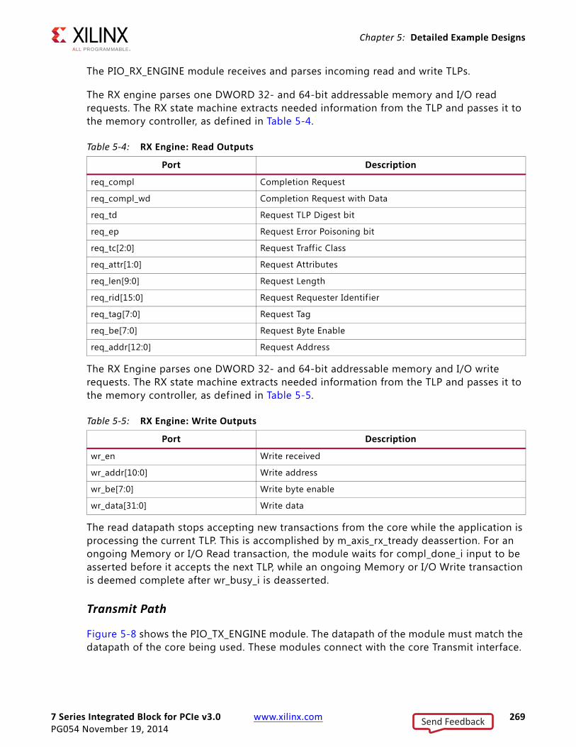
7 Series Integrated Block for PCIe v3.0 www.xilinx.com 269PG054 November 19, 2014
Chapter 5: Detailed Example Designs
The PIO_RX_ENGINE module receives and parses incoming read and write TLPs.
The RX engine parses one DWORD 32- and 64-bit addressable memory and I/O read requests. The RX state machine extracts needed information from the TLP and passes it to the memory controller, as defined in Table 5-4.
The RX Engine parses one DWORD 32- and 64-bit addressable memory and I/O write requests. The RX state machine extracts needed information from the TLP and passes it to the memory controller, as defined in Table 5-5.
The read datapath stops accepting new transactions from the core while the application is processing the current TLP. This is accomplished by m_axis_rx_tready deassertion. For an ongoing Memory or I/O Read transaction, the module waits for compl_done_i input to be asserted before it accepts the next TLP, while an ongoing Memory or I/O Write transaction is deemed complete after wr_busy_i is deasserted.
Transmit Path
Figure 5-8 shows the PIO_TX_ENGINE module. The datapath of the module must match the datapath of the core being used. These modules connect with the core Transmit interface.
Table 5-4: RX Engine: Read Outputs
Port Description
req_compl Completion Request
req_compl_wd Completion Request with Data
req_td Request TLP Digest bit
req_ep Request Error Poisoning bit
req_tc[2:0] Request Traff ic Class
req_attr[1:0] Request Attributes
req_len[9:0] Request Length
req_rid[15:0] Request Requester Identif ier
req_tag[7:0] Request Tag
req_be[7:0] Request Byte Enable
req_addr[12:0] Request Address
Table 5-5: RX Engine: Write Outputs
Port Description
wr_en Write received
wr_addr[10:0] Write address
wr_be[7:0] Write byte enable
wr_data[31:0] Write data
Send Feedback
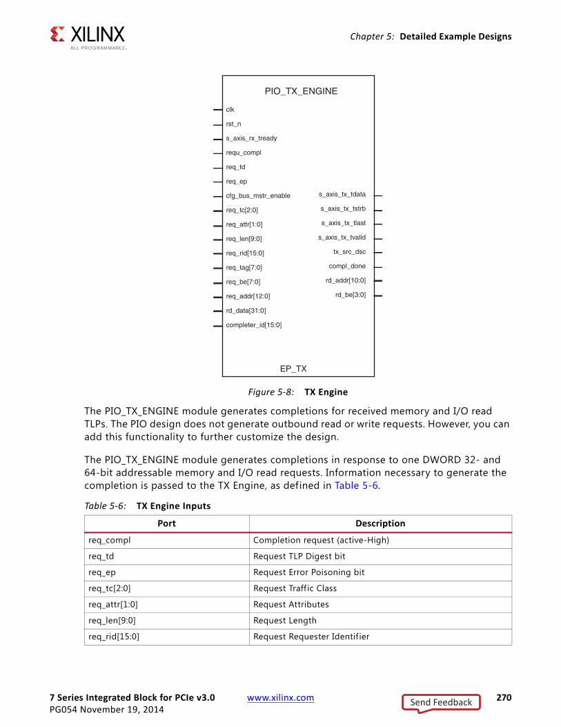
7 Series Integrated Block for PCIe v3.0 www.xilinx.com 270PG054 November 19, 2014
Chapter 5: Detailed Example Designs
The PIO_TX_ENGINE module generates completions for received memory and I/O read TLPs. The PIO design does not generate outbound read or write requests. However, you can add this functionality to further customize the design.
The PIO_TX_ENGINE module generates completions in response to one DWORD 32- and 64-bit addressable memory and I/O read requests. Information necessary to generate the completion is passed to the TX Engine, as defined in Table 5-6.
X-Ref Target - Figure 5-8
Figure 5-8: TX Engine
Table 5-6: TX Engine Inputs
Port Description
req_compl Completion request (active-High)
req_td Request TLP Digest bit
req_ep Request Error Poisoning bit
req_tc[2:0] Request Traff ic Class
req_attr[1:0] Request Attributes
req_len[9:0] Request Length
req_rid[15:0] Request Requester Identif ier
clk
rst_n
s_axis_rx_tready
requ_compl
req_td
req_ep
cfg_bus_mstr_enable
req_tc[2:0]
req_attr[1:0]
req_len[9:0]
req_rid[15:0]
req_tag[7:0]
req_be[7:0]
req_addr[12:0]
rd_data[31:0]
completer_id[15:0]
s_axis_tx_tdata
s_axis_tx_tstrb
s_axis_tx_tlast
s_axis_tx_tvalid
tx_src_dsc
compl_done
rd_addr[10:0]
rd_be[3:0]
PIO_TX_ENGINE
EP_TX
Send Feedback

7 Series Integrated Block for PCIe v3.0 www.xilinx.com 271PG054 November 19, 2014
Chapter 5: Detailed Example Designs
After the completion is sent, the TX engine asserts the compl_done_i output indicating to the RX engine that it can assert m_axis_rx_tready and continue receiving TLPs.
Endpoint Memory
Figure 5-9 displays the PIO_EP_MEM_ACCESS module. This module contains the Endpoint memory space.
The PIO_EP_MEM_ACCESS module processes data written to the memory from incoming Memory and I/O Write TLPs and provides data read from the memory in response to Memory and I/O Read TLPs.
The EP_MEM module processes one DWORD 32- and 64-bit addressable Memory and I/O Write requests based on the information received from the RX Engine, as defined in Table 5-7. While the memory controller is processing the write, it asserts the wr_busy_o output indicating it is busy.
req_tag[7:0] Request Tag
req_be[7:0] Request Byte Enable
req_addr[12:0] Request Address
X-Ref Target - Figure 5-9
Figure 5-9: EP Memory Access
Table 5-6: TX Engine Inputs (Cont’d)
Port Description
clk
rst_n
wr_en_i
rd_addr_i[10:0]
rd_be_i[3:0]
wr_addr_i[10:0]
wr_be_i[7:0]
wr_data_i[31:0]
wr_busy_o
rd_data_o[31:0]
PIO_EP_MEM_ACCESS
EP_MEM
Send Feedback
7 Series Integrated Block for PCIe v3.0 www.xilinx.com 272PG054 November 19, 2014
Chapter 5: Detailed Example Designs
Both 32- and 64-bit Memory and I/O Read requests of one DWORD are processed based on the inputs defined in Table 5-8. After the read request is processed, the data is returned on rd_data_o[31:0].
PIO Operation
PIO Read Transaction
Figure 5-10 depicts a Back-to-Back Memory Read request to the PIO design. The receive engine deasserts m_axis_rx_tready as soon as the f irst TLP is completely received. The next Read transaction is accepted only after compl_done_o is asserted by the transmit engine, indicating that Completion for the first request was successfully transmitted.
Table 5-7: EP Memory: Write Inputs
Port Description
wr_en_i Write received
wr_addr_i[10:0] Write address
wr_be_i[7:0] Write byte enable
wr_data_i[31:0] Write data
Table 5-8: EP Memory: Read Inputs
Port Description
req_be_i[7:0] Request Byte Enable
req_addr_i[31:0] Request Address
Send Feedback

7 Series Integrated Block for PCIe v3.0 www.xilinx.com 273PG054 November 19, 2014
Chapter 5: Detailed Example Designs
PIO Write Transaction
Figure 5-11 depicts a back-to-back Memory Write to the PIO design. The next Write transaction is accepted only after wr_busy_o is deasserted by the memory access unit, indicating that data associated with the f irst request was successfully written to the memory aperture.
X-Ref Target - Figure 5-10
Figure 5-10: Back-to-Back Read Transactions
user_clk_out
m_axis_rx_tdata[63:0]
m_axis_rx_tkeep[7:0]
m_axis_rx_tlast
m_axis_rx_tvalid
m_axis_rx_tready
(rx_bar_hit[7:0])m_axis_rx_tuser[9:2]
compl_done_o
s_axis_tx_tdata[63:0]
s_axis_tx_tkeep[7:0]
s_axis_tx_tlast
s_axis_tx_tvalid
(src_dsc)s_axis_tx_tuser[3]
s_axis_tx_tready
H1H0 --H2 H1H0 --H3
FFh 0Fh FFh 0Fh FFh
00h 01h 00h 01h 00h
H1H0 D0H2
FF
TLP1 TLP2
Send Feedback
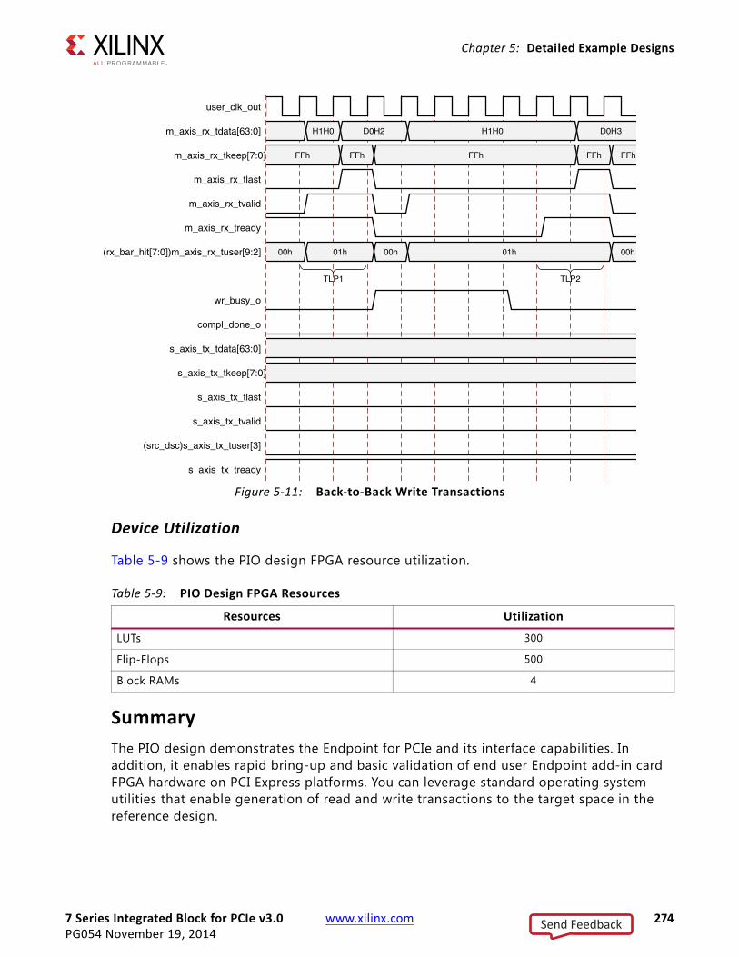
7 Series Integrated Block for PCIe v3.0 www.xilinx.com 274PG054 November 19, 2014
Chapter 5: Detailed Example Designs
Device Utilization
Table 5-9 shows the PIO design FPGA resource utilization.
SummaryThe PIO design demonstrates the Endpoint for PCIe and its interface capabilities. In addition, it enables rapid bring-up and basic validation of end user Endpoint add-in card FPGA hardware on PCI Express platforms. You can leverage standard operating system utilities that enable generation of read and write transactions to the target space in the reference design.
X-Ref Target - Figure 5-11
Figure 5-11: Back-to-Back Write Transactions
user_clk_out
m_axis_rx_tdata[63:0]
m_axis_rx_tkeep[7:0]
m_axis_rx_tlast
m_axis_rx_tvalid
m_axis_rx_tready
(rx_bar_hit[7:0])m_axis_rx_tuser[9:2]
wr_busy_o
compl_done_o
s_axis_tx_tdata[63:0]
s_axis_tx_tkeep[7:0]
s_axis_tx_tlast
s_axis_tx_tvalid
(src_dsc)s_axis_tx_tuser[3]
s_axis_tx_tready
H1H0 D0H2 H1H0 D0H3
FFh FFh FFh FFh FFh
00h 01h 00h 01h 00h
TLP1 TLP2
Table 5-9: PIO Design FPGA Resources
Resources Utilization
LUTs 300
Flip-Flops 500
Block RAMs 4
Send Feedback
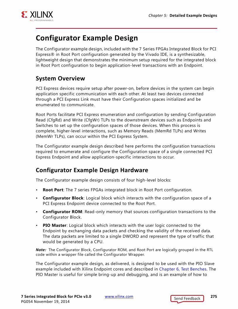
7 Series Integrated Block for PCIe v3.0 www.xilinx.com 275PG054 November 19, 2014
Chapter 5: Detailed Example Designs
Configurator Example DesignThe Configurator example design, included with the 7 Series FPGAs Integrated Block for PCI Express® in Root Port configuration generated by the Vivado IDE, is a synthesizable, lightweight design that demonstrates the minimum setup required for the integrated block in Root Port configuration to begin application-level transactions with an Endpoint.
System OverviewPCI Express devices require setup after power-on, before devices in the system can begin application specific communication with each other. At least two devices connected through a PCI Express Link must have their Configuration spaces initialized and be enumerated to communicate.
Root Ports facilitate PCI Express enumeration and configuration by sending Configuration Read (CfgRd) and Write (CfgWr) TLPs to the downstream devices such as Endpoints and Switches to set up the configuration spaces of those devices. When this process is complete, higher-level interactions, such as Memory Reads (MemRd TLPs) and Writes (MemWr TLPs), can occur within the PCI Express System.
The Configurator example design described here performs the configuration transactions required to enumerate and configure the Configuration space of a single connected PCI Express Endpoint and allow application-specific interactions to occur.
Configurator Example Design HardwareThe Configurator example design consists of four high-level blocks:
• Root Port: The 7 series FPGAs integrated block in Root Port configuration.
• Configurator Block : Logical block which interacts with the configuration space of a PCI Express Endpoint device connected to the Root Port.
• Configurator ROM: Read-only memory that sources configuration transactions to the Configurator Block.
• PIO Master : Logical block which interacts with the user logic connected to the Endpoint by exchanging data packets and checking the validity of the received data. The data packets are limited to a single DWORD and represent the type of traffic that would be generated by a CPU.
Note: The Configurator Block, Configurator ROM, and Root Port are logically grouped in the RTL code within a wrapper f ile called the Configurator Wrapper.
The Configurator example design, as delivered, is designed to be used with the PIO Slave example included with Xilinx Endpoint cores and described in Chapter 6, Test Benches. The PIO Master is useful for simple bring-up and debugging, and is an example of how to
Send Feedback
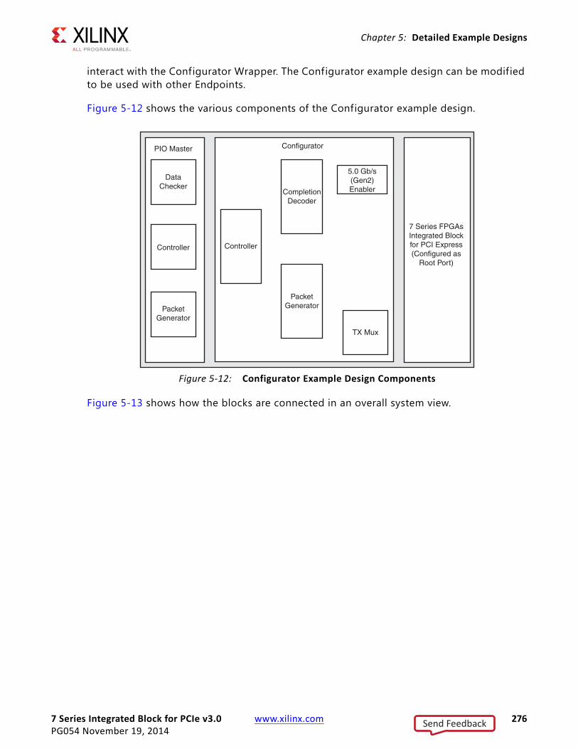
7 Series Integrated Block for PCIe v3.0 www.xilinx.com 276PG054 November 19, 2014
Chapter 5: Detailed Example Designs
interact with the Configurator Wrapper. The Configurator example design can be modified to be used with other Endpoints.
Figure 5-12 shows the various components of the Configurator example design.
Figure 5-13 shows how the blocks are connected in an overall system view.
X-Ref Target - Figure 5-12
Figure 5-12: Configurator Example Design Components
ConfiguratorPIO Master
DataChecker
Controller
PacketGenerator
Controller
CompletionDecoder
PacketGenerator
5.0 Gb/s(Gen2)Enabler
TX Mux
7 Series FPGAsIntegrated Blockfor PCI Express(Configured as
Root Port)
Send Feedback
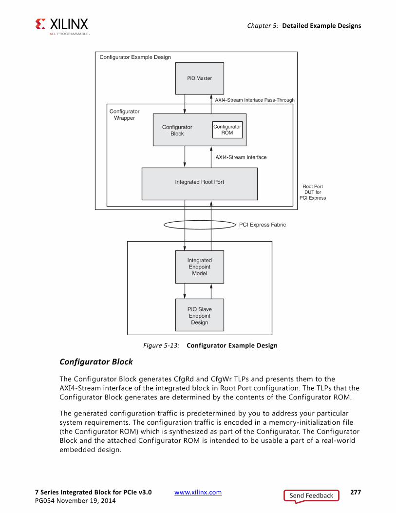
7 Series Integrated Block for PCIe v3.0 www.xilinx.com 277PG054 November 19, 2014
Chapter 5: Detailed Example Designs
Configurator Block
The Configurator Block generates CfgRd and CfgWr TLPs and presents them to the AXI4-Stream interface of the integrated block in Root Port configuration. The TLPs that the Configurator Block generates are determined by the contents of the Configurator ROM.
The generated configuration traffic is predetermined by you to address your particular system requirements. The configuration traffic is encoded in a memory-initialization file (the Configurator ROM) which is synthesized as part of the Configurator. The Configurator Block and the attached Configurator ROM is intended to be usable a part of a real-world embedded design.
X-Ref Target - Figure 5-13
Figure 5-13: Configurator Example Design
PIO Master
ConfiguratorWrapper
ConfiguratorBlock
ConfiguratorROM
Integrated Root Port
PCI Express Fabric
IntegratedEndpoint
Model
PIO SlaveEndpointDesign
Configurator Example Design
AXI4-Stream Interface Pass-Through
Root PortDUT for
PCI Express
AXI4-Stream Interface
Send Feedback

7 Series Integrated Block for PCIe v3.0 www.xilinx.com 278PG054 November 19, 2014
Chapter 5: Detailed Example Designs
The Configurator Block steps through the Configuration ROM file and sends the TLPs specified therein. Supported TLP types are Message, Message w/Data, Configuration Write (Type 0), and Configuration Read (Type 0). For the Configuration packets, the Configurator Block waits for a Completion to be returned before transmitting the next TLP. If the Completion TLP f ields do not match the expected values, PCI Express configuration fails. However, the Data f ield of Completion TLPs is ignored and not checked
Note: There is no completion timeout mechanism in the Configurator Block, so if no Completion is returned, the Configurator Block waits forever.
The Configurator Block has these parameters, which you can alter:
• TCQ: Clock-to-out delay modeled by all registers in design.
• EXTRA_PIPELINE: Controls insertion of an extra pipeline stage on the Receive AXI4-Stream interface for timing.
• ROM_FILE: File name containing conf iguration steps to perform.
• ROM_SIZE: Number of lines in ROM_FILE containing data (equals number of TLPs to send/2).
• REQUESTER_ID: Value for the Requester ID f ield in outgoing TLPs.
When the Configurator Block design is used, all TLP traff ic must pass through the Configurator Block. The user design is responsible for asserting the start_config input (for one clock cycle) to initiate the configuration process when user_lnk_up has been asserted by the core. Following start_config, the Configurator Block performs whatever configuration steps have been specified in the Configuration ROM. During configuration, the Configurator Block controls the core AXI4-Stream interface. Following configuration, all AXI4-Stream traffic is routed to/from the user application, which in the case of this example design is the PIO Master. The end of configuration is signaled by the assertion of f inished_config. If configuration is unsuccessful for some reason, failed_config is also asserted.
If used in a system that supports PCIe® v2.2 5.0 Gb/s links, the Configurator Block begins its process by attempting to up-train the link from 2.5 Gb/s to 5.0 Gb/s. This feature is enabled depending on the LINK_CAP_MAX_LINK_SPEED parameter on the Configurator Wrapper.
The Configurator does not support the user throttling received data on the Receive AXI4-Stream interface. Because of this, the Root Port inputs which control throttling are not included on the Configurator Wrapper. These signals are m_axis_rx_tready and rx_np_ok . This is a limitation of the Configurator example design and not of the core in Root Port configuration. This means that the user design interfacing with the Configurator Example Design must be able to accept received data at line rate.
Send Feedback
7 Series Integrated Block for PCIe v3.0 www.xilinx.com 279PG054 November 19, 2014
Chapter 5: Detailed Example Designs
Configurator ROM
The Configurator ROM stores the necessary configuration transactions to configure a PCI Express Endpoint. This ROM interfaces with the Configurator Block to send these transactions over the PCI Express link.
The example ROM file included with this design shows the operations needed to configure a 7 Series FPGAs Integrated Endpoint Block for PCI Express and PIO Example Design.
The Configurator ROM can be customized for other Endpoints and PCI Express system topologies. The unique set of configuration transactions required depends on the Endpoint that interacts with the Root Port. This information can be obtained from the documentation provided with the Endpoint.
The ROM file follows the format specif ied in the Verilog specif ication (IEEE 1364-2001) section 17.2.8, which describes using the $readmemb function to pre-load data into a RAM or ROM. Verilog-style comments are allowed.
The file is read by the simulator or synthesis tool and each memory value encountered is used as a single location in memory. Digits can be separated by an underscore character (_) for clarity without constituting a new location.
Each configuration transaction specif ied uses two adjacent memory locations:
• The first location specif ies the header f ields. Header fields are on even addresses.
• The second location specif ies the 32-bit data payload. (For CfgRd TLPs and Messages without data, the data location is unused but still present.) Data payloads are on odd addresses.
For headers, Messages and CfgRd/CfgWr TLPs use different fields. For all TLPs, two bits specify the TLP type. For Messages, Message Routing and Message Code are specif ied. For CfgRd/CfgWr TLPs, Function Number, Register Number, and 1st DWORD Byte-Enable are specified. The specif ic bit layout is shown in the example ROM file.
PIO Master
The PIO Master demonstrates how a user application design might interact with the Configurator Block. It directs the Configurator Block to bring up the link partner at the appropriate time, and then (after successful bring-up) generates and consumes bus traffic. The PIO Master performs writes and reads across the PCI Express Link to the PIO Slave Example Design (from the Endpoint core) to confirm basic operation of the link and the Endpoint.
The PIO Master waits until user_lnk_up is asserted by the Root Port. It then asserts start_config to the Configurator Block. When the Configurator Block asserts f inished_config, the PIO Master writes and reads to/from each BAR in the PIO Slave design. If the readback data matches what was written, the PIO Master asserts its
Send Feedback
7 Series Integrated Block for PCIe v3.0 www.xilinx.com 280PG054 November 19, 2014
Chapter 5: Detailed Example Designs
pio_test_finished output. If there is a data mismatch or the Configurator Block fails to configure the Endpoint, the PIO Master asserts its pio_test_failed output. The PIO Master operation can be restarted by asserting its pio_test_restart input for one clock cycle.
Configurator File Structure
Table 5-10 defines the Configurator example design file structure.
The hierarchy of the Configurator example design is:
• xilinx_pcie_2_1_rport_7x topdirectory
° cgator_wrapper
- pcie_2_1_rport_7x (in the source directory)This directory contains all the source f iles for the core in Root Port Configuration.
- cgator
- cgator_cpl_decoder
- cgator_pkt_generator
- cgator_tx_mux
- cgator_gen2_enabler
- cgator_controllerThis directory contains <cgator_cfg_rom.data> (specif ied by ROM_FILE)*
Table 5-10: Example Design File Structure
File Description
xilinx_pcie_2_1_rport_7x.v Top-level wrapper f ile for Configurator example design
cgator_wrapper.v Wrapper for Configurator and Root Port
cgator.v Wrapper for Configurator sub-blocks
cgator_cpl_decoder.v Completion decoder
cgator_pkt_generator.v Configuration TLP generator
cgator_tx_mux.v Transmit AXI4-Stream muxing logic
cgator_gen2_enabler.v 5.0 Gb/s directed speed change module
cgator_controller.v Configurator transmit engine
cgator_cfg_rom.data Configurator ROM file
pio_master.v Wrapper for PIO Master
pio_master_controller.v TX and RX Engine for PIO Master
pio_master_checker.v Checks incoming User-Application Completion TLPs
pio_master_pkt_generator.v Generates User-Application TLPs
Send Feedback
7 Series Integrated Block for PCIe v3.0 www.xilinx.com 281PG054 November 19, 2014
Chapter 5: Detailed Example Designs
° pio_master
- pio_master_controller
- pio_master_checker
- pio_master_pkt_generator
Note: cgator_cfg_rom.data is the default name of the ROM data f ile. You can override this by changing the value of the ROM_FILE parameter.
SummaryThe Configurator example design is a synthesizable design that demonstrates the capabilities of the 7 Series FPGAs Integrated Block for PCI Express when configured as a Root Port. The example is provided through the Vivado IDE and uses the Endpoint PIO example as a target for PCI Express enumeration and configuration. The design can be modif ied to target other Endpoints by changing the contents of a ROM file.
Generating the Core To generate a core using the default values in the Vivado IDE, follow these steps:
1. Start the Vivado IP catalog.
2. Select File > New Project.
3. Enter a project name and location, then click Next. This example uses project_name.cpg and project_dir.
4. In the New Project wizard pages, do not add sources, existing IP, or constraints.
5. From the Part tab (Figure 5-14), select these options:
° Family: Virtex7
° Device: xc7v485t
° Package: ffg1157
° Speed Grade: -3
Send Feedback

7 Series Integrated Block for PCIe v3.0 www.xilinx.com 282PG054 November 19, 2014
Chapter 5: Detailed Example Designs
Note: If an unsupported silicon device is selected, the core is dimmed (unavailable) in the list of cores.
6. In the final project summary page, click OK.
7. In the Vivado IP catalog, expand Standard Bus Interfaces > PCI Express, and double-click the 7 Series Integrated Block for PCI Express core to display the Customize IP dialog box.
8. In the Component Name field, enter a name for the core.
Note: <component_name> is used in this example.
X-Ref Target - Figure 5-14
Figure 5-14: Default Part
Send Feedback
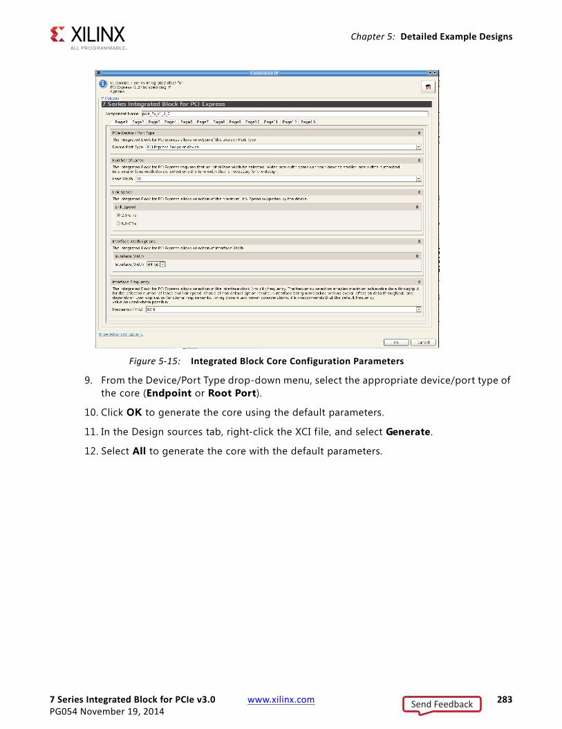
7 Series Integrated Block for PCIe v3.0 www.xilinx.com 283PG054 November 19, 2014
Chapter 5: Detailed Example Designs
9. From the Device/Port Type drop-down menu, select the appropriate device/port type of the core (Endpoint or Root Port).
10. Click OK to generate the core using the default parameters.
11. In the Design sources tab, right-click the XCI f ile, and select Generate.
12. Select All to generate the core with the default parameters.
X-Ref Target - Figure 5-15
Figure 5-15: Integrated Block Core Configuration Parameters
Send Feedback
7 Series Integrated Block for PCIe v3.0 www.xilinx.com 284PG054 November 19, 2014
Chapter 5: Detailed Example Designs
Simulating the Example DesignThe example design provides a quick way to simulate and observe the behavior of the core for PCI Express Endpoint and Root Port Example design projects generated using the Vivado Design Suite.
The currently supported simulators are:
• Vivado simulator (default)
• ModelSim Questa SIM
Note: ModelSim PE 10.2a is not supported.
• Cadence IES
• Synopsys VCS
The simulator uses the example design test bench and test cases provided along with the example design for both of the design configurations.
For any project (PCI Express core) generated out of the box, the simulation using the default Vivado simulator can be run as follows:
1. In the Sources Window, right-click the example project f ile (.xci), and select Open IP Example Design.
The example project is created.
2. In the Flow Navigator (left-hand pane), under Simulation, right-click Run Simulation and select Run Behavioral Simulation.
IMPORTANT: The post-synthesis and post-implementation simulation options are not supported for the PCI Express block.
After the Run Behavioral Simulation Option is running, you can observe the compilation and elaboration phase through the activity in the Tcl Console, and in the Simulation tab of the Log Window.
3. In Tcl Console, type the run all command and press Enter. This runs the complete simulation as per the test case provided in example design test bench.
After the simulation is complete, the result can be viewed in the Tcl Console.
In Vivado IDE, change the simulation settings as follows:
1. In the Flow Navigator, under Simulation, select Simulation Settings.
Send Feedback
7 Series Integrated Block for PCIe v3.0 www.xilinx.com 285PG054 November 19, 2014
Chapter 5: Detailed Example Designs
2. Set the Target simulator to QuestaSim/ModelSim Simulator, Incisive Enterprise Simulator (IES) or Verilog Compiler Simulator.
3. In the simulator tab, select Run Simulation > Run behavioral simulation.
4. When prompted, click Yes to change and then run the simulator.
IMPORTANT: Simulation is not supported for configurations with the Silicon Revision option set to Initial_ES. Only implementation is supported. If simulation is performed, it results in DRP monitor errors.
Endpoint ConfigurationThe simulation environment provided with the 7 Series FPGAs Integrated Block for PCI Express core in Endpoint configuration performs simple memory access tests on the PIO example design. Transactions are generated by the Root Port Model and responded to by the PIO example design.
• PCI Express Transaction Layer Packets (TLPs) are generated by the test bench transmit user application (pci_exp_usrapp_tx). As it transmits TLPs, it also generates a log f ile, tx.dat.
• PCI Express TLPs are received by the test bench receive user application (pci_exp_usrapp_rx). As the user application receives the TLPs, it generates a log f ile, rx.dat.
For more information about the test bench, see Root Port Model Test Bench for Endpoint in Chapter 6.
Synthesizing and Implementing the Example DesignTo run synthesis and implementation on the example design:
1. Right-click the XCI f ile, and select Open IP example design.
A new Vivado IDE window opens with the project name example_project within the project directory.
2. In the Flow Navigator, click Run Synthesis and Run Implementation.
TIP: Click Run Implementation to run both synthesis and implementation. Click Generate Bitstream to run synthesis, implementation, and then generate the bitstream.
Send Feedback
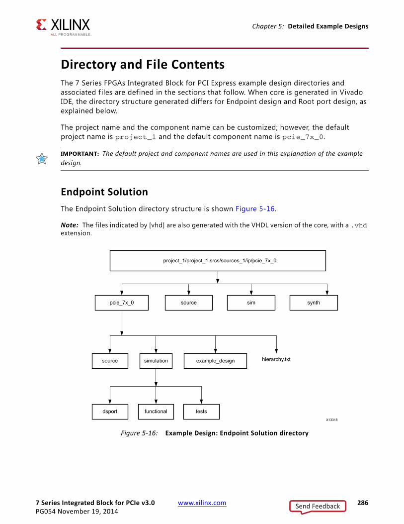
7 Series Integrated Block for PCIe v3.0 www.xilinx.com 286PG054 November 19, 2014
Chapter 5: Detailed Example Designs
Directory and File ContentsThe 7 Series FPGAs Integrated Block for PCI Express example design directories and associated f iles are defined in the sections that follow. When core is generated in Vivado IDE, the directory structure generated differs for Endpoint design and Root port design, as explained below.
The project name and the component name can be customized; however, the default project name is project_1 and the default component name is pcie_7x_0.
IMPORTANT: The default project and component names are used in this explanation of the example design.
Endpoint SolutionThe Endpoint Solution directory structure is shown Figure 5-16.
Note: The f iles indicated by [vhd] are also generated with the VHDL version of the core, with a .vhd extension.X-Ref Target - Figure 5-16
Figure 5-16: Example Design: Endpoint Solution directory
Send Feedback
7 Series Integrated Block for PCIe v3.0 www.xilinx.com 287PG054 November 19, 2014
Chapter 5: Detailed Example Designs
project_1/project_1.src/sources_1/ip/pcie_7x_0
This is the main directory for all directories. The name of the directory is project_1, by default.
pcie_7x_0
This is the directory created based on the component name specified. By default this directory is pcie_7x_0. This directory consists of three subdirectories: source, simulation and example_design. These are described in detail in the following sections.
source
This directory contains the core top-level module definition. This module is instantiated in the Vivado Design Suite-generated top-level wrapper f ile, which exists in the sim and synth directories, in parallel to this directory.
File name (Verilog format): pcie_7x_<version_number>_top.v. For example: pcie_7x_v2_1_top.v.
File name (VHDL format): pcie_7x_<version_number>_top.vhd. For example: pcie_7x_v2_1_top.vhd.
sim
This directory contains the Vivado Design Suite-generated top-level wrapper f ile used for simulation. The f ile name is based on the component name you have specif ied. The default name is pcie_7x_0.v. This f ile contains the core top-level module definition which instantiates the module pcie_7x_<version_number>_top.v or pcie_7x_<version_number>_top.vhd.
synth
This directory contains the Vivado Design Suite-generated top-level wrapper f ile used for synthesis. The f ile name is based the component name you have specif ied. The default name is pcie_7x_0.v. This f ile contains the core top-level module definition which instantiates the module pcie_7x_<version_number>_top.v or pcie_7x_<version_number>_top.vhd.
Send Feedback
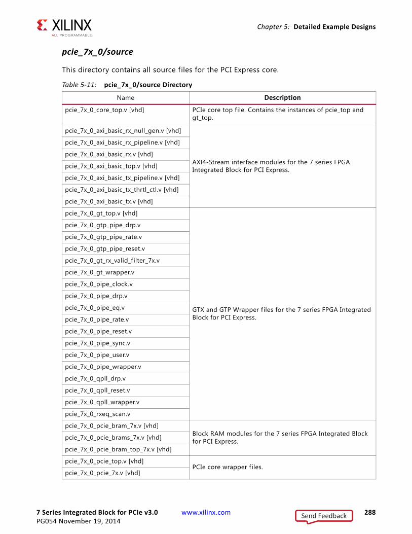
7 Series Integrated Block for PCIe v3.0 www.xilinx.com 288PG054 November 19, 2014
Chapter 5: Detailed Example Designs
pcie_7x_0/source
This directory contains all source files for the PCI Express core.
Table 5-11: pcie_7x_0/source Directory
Name Description
pcie_7x_0_core_top.v [vhd] PCIe core top file. Contains the instances of pcie_top and gt_top.
pcie_7x_0_axi_basic_rx_null_gen.v [vhd]
AXI4-Stream interface modules for the 7 series FPGA Integrated Block for PCI Express.
pcie_7x_0_axi_basic_rx_pipeline.v [vhd]
pcie_7x_0_axi_basic_rx.v [vhd]
pcie_7x_0_axi_basic_top.v [vhd]
pcie_7x_0_axi_basic_tx_pipeline.v [vhd]
pcie_7x_0_axi_basic_tx_thrtl_ctl.v [vhd]
pcie_7x_0_axi_basic_tx.v [vhd]
pcie_7x_0_gt_top.v [vhd]
GTX and GTP Wrapper f iles for the 7 series FPGA Integrated Block for PCI Express.
pcie_7x_0_gtp_pipe_drp.v
pcie_7x_0_gtp_pipe_rate.v
pcie_7x_0_gtp_pipe_reset.v
pcie_7x_0_gt_rx_valid_f ilter_7x.v
pcie_7x_0_gt_wrapper.v
pcie_7x_0_pipe_clock.v
pcie_7x_0_pipe_drp.v
pcie_7x_0_pipe_eq.v
pcie_7x_0_pipe_rate.v
pcie_7x_0_pipe_reset.v
pcie_7x_0_pipe_sync.v
pcie_7x_0_pipe_user.v
pcie_7x_0_pipe_wrapper.v
pcie_7x_0_qpll_drp.v
pcie_7x_0_qpll_reset.v
pcie_7x_0_qpll_wrapper.v
pcie_7x_0_rxeq_scan.v
pcie_7x_0_pcie_bram_7x.v [vhd]Block RAM modules for the 7 series FPGA Integrated Block for PCI Express.pcie_7x_0_pcie_brams_7x.v [vhd]
pcie_7x_0_pcie_bram_top_7x.v [vhd]
pcie_7x_0_pcie_top.v [vhd]PCIe core wrapper f iles.
pcie_7x_0_pcie_7x.v [vhd]
Send Feedback
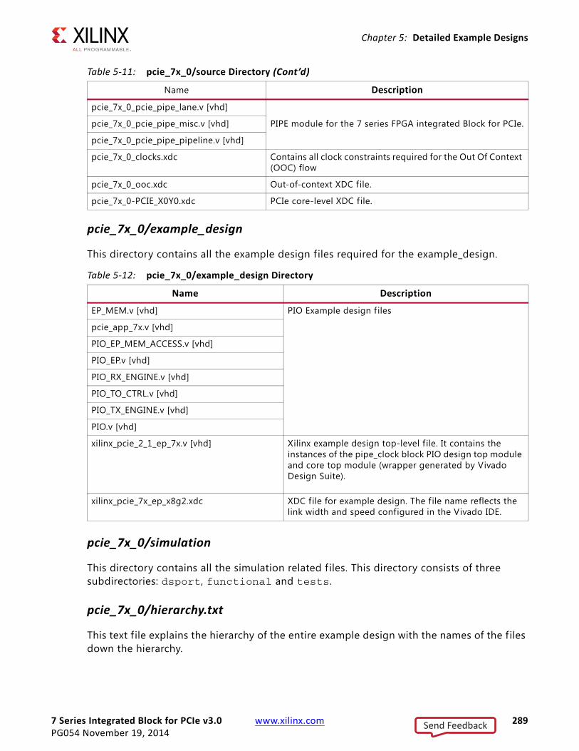
7 Series Integrated Block for PCIe v3.0 www.xilinx.com 289PG054 November 19, 2014
Chapter 5: Detailed Example Designs
pcie_7x_0/example_design
This directory contains all the example design files required for the example_design.
pcie_7x_0/simulation
This directory contains all the simulation related f iles. This directory consists of three subdirectories: dsport, functional and tests.
pcie_7x_0/hierarchy.txt
This text f ile explains the hierarchy of the entire example design with the names of the f iles down the hierarchy.
pcie_7x_0_pcie_pipe_lane.v [vhd]
PIPE module for the 7 series FPGA integrated Block for PCIe.pcie_7x_0_pcie_pipe_misc.v [vhd]
pcie_7x_0_pcie_pipe_pipeline.v [vhd]
pcie_7x_0_clocks.xdc Contains all clock constraints required for the Out Of Context (OOC) flow
pcie_7x_0_ooc.xdc Out-of-context XDC file.
pcie_7x_0-PCIE_X0Y0.xdc PCIe core-level XDC file.
Table 5-12: pcie_7x_0/example_design Directory
Name Description
EP_MEM.v [vhd] PIO Example design f iles
pcie_app_7x.v [vhd]
PIO_EP_MEM_ACCESS.v [vhd]
PIO_EP.v [vhd]
PIO_RX_ENGINE.v [vhd]
PIO_TO_CTRL.v [vhd]
PIO_TX_ENGINE.v [vhd]
PIO.v [vhd]
xilinx_pcie_2_1_ep_7x.v [vhd] Xilinx example design top-level f ile. It contains the instances of the pipe_clock block PIO design top module and core top module (wrapper generated by Vivado Design Suite).
xilinx_pcie_7x_ep_x8g2.xdc XDC file for example design. The f ile name reflects the link width and speed configured in the Vivado IDE.
Table 5-11: pcie_7x_0/source Directory (Cont’d)
Name Description
Send Feedback

7 Series Integrated Block for PCIe v3.0 www.xilinx.com 290PG054 November 19, 2014
Chapter 5: Detailed Example Designs
pcie_7x_0/simulation/dsport
This directory contains the dsport model f iles.
pcie_7x_0/simulation/functional
This directory consists of the top-level test bench and clock generation modules.
pcie_7x_0/simulation/tests
This directory consists of the test cases.
Root Port SolutionThe Root Port Solution directory structure is shown in Figure 5-17. The f ile directory structure is same as Endpoint solution except the simulation directory.
Table 5-13: pcie_7x_0/simulation/dsport Directory
Name Description
pcie_2_1_rport_7x.v [vhd]
Root port models f iles
pcie_axi_trn_bridge.v [vhd]
pci_exp_expect_tasks.vh
pci_exp_usrapp_cfg.v [vhd]
pci_exp_usrapp_com.v [vhd]
pci_exp_usrapp_pl.v [vhd]
pci_exp_usrapp_rx.v [vhd]
pci_exp_usrapp_tx.v [vhd]
xilinx_pcie_2_1_rport_7x.v [vhd]
Table 5-14: pcie_7x_0/simulation/functional Directory
Name Description
board_common.vh Contains test bench definitions.
board.v [vhd] Top-level test bench f ile.
sys_clk_gen_ds.v [vhd] System differential clock source.
sys_clk_gen.v [vhd] System clock source.
Table 5-15: pcie_7x_0/simulation/tests Directory
Name Description
sample_tests.vhTest definition for example test bench.
tests.vh
Send Feedback

7 Series Integrated Block for PCIe v3.0 www.xilinx.com 291PG054 November 19, 2014
Chapter 5: Detailed Example Designs
Note: The f iles indicated by [vhd] are also generated with the VHDL version of the core, with a .vhd extension.
project_1/project_1.src/sources_1/ip/pcie_7x_0
This is the main directory for all directories. The name of the directory is project_1, by default.
pcie_7x_0
This directory is created based on the component name specif ied. By default this directory is pcie_7x_0. It consists of three subdirectories: source, simulation and example_design. These are described in detail in the following sections.
source
This directory contains the core top-level module definition. This module is instantiated in the Vivado Design Suite-generated top-level wrapper f ile, which exists in the sim and synth directories, in parallel to this directory.
File name (Verilog format): pcie_7x_<version_number>_top.v. For example: pcie_7x_v2_1_top.v.
File name (VHDL format): pcie_7x_<version_number>_top.vhd. For example: pcie_7x_v2_1_top.vhd.
X-Ref Target - Figure 5-17
Figure 5-17: Example Design: Root Port Solution Directory Structure
Send Feedback

7 Series Integrated Block for PCIe v3.0 www.xilinx.com 292PG054 November 19, 2014
Chapter 5: Detailed Example Designs
sim
This directory contains the Vivado Design Suite-generated top-level wrapper f ile used for simulation. The f ile name is based on the component name you have specif ied. The default name is pcie_7x_0.v. This f ile contains the core top-level module definition which instantiates the module pcie_7x_<version_number>_top.v or pcie_7x_<version_number>_top.vhd.
synth
This directory contains the Vivado Design Suite-generated top-level wrapper f ile used for synthesis. The f ile name is based the component name you have specif ied. The default name is pcie_7x_0.v. This f ile contains the core top-level module definition which instantiates the module pcie_7x_<version_number>_top.v or pcie_7x_<version_number>_top.vhd.
pcie_7x_0/source
This directory contains all source files for the PCI Express core.
Table 5-16: pcie_7x_0/source Directory
Name Description
pcie_7x_0_core_top.v [vhd] PCIe core top file. Contains the instances of pcie_top and gt_top.
pcie_7x_0_axi_basic_rx_null_gen.v [vhd]
AXI4-Stream interface modules for the 7 series FPGA Integrated Block for PCI Express.
pcie_7x_0_axi_basic_rx_pipeline.v [vhd]
pcie_7x_0_axi_basic_rx.v [vhd]
pcie_7x_0_axi_basic_top.v [vhd]
pcie_7x_0_axi_basic_tx_pipeline.v [vhd]
pcie_7x_0_axi_basic_tx_thrtl_ctl.v [vhd]
pcie_7x_0_axi_basic_tx.v [vhd]
Send Feedback

7 Series Integrated Block for PCIe v3.0 www.xilinx.com 293PG054 November 19, 2014
Chapter 5: Detailed Example Designs
pcie_7x_0_gt_top.v [vhd]
GTX and GTP Wrapper f iles for the 7 series FPGA Integrated Block for PCI Express.
pcie_7x_0_gtp_pipe_drp.v
pcie_7x_0_gtp_pipe_rate.v
pcie_7x_0_gtp_pipe_reset.v
pcie_7x_0_gt_rx_valid_f ilter_7x.v
pcie_7x_0_gt_wrapper.v
pcie_7x_0_pipe_clock.v
pcie_7x_0_pipe_drp.v
pcie_7x_0_pipe_eq.v
pcie_7x_0_pipe_rate.v
pcie_7x_0_pipe_reset.v
pcie_7x_0_pipe_sync.v
pcie_7x_0_pipe_user.v
pcie_7x_0_pipe_wrapper.v
pcie_7x_0_qpll_drp.v
pcie_7x_0_qpll_reset.v
pcie_7x_0_qpll_wrapper.v
pcie_7x_0_rxeq_scan.v
pcie_7x_0_pcie_bram_7x.v [vhd]Block RAM modules for the 7 series FPGA Integrated Block for PCI Express.pcie_7x_0_pcie_brams_7x.v [vhd]
pcie_7x_0_pcie_bram_top_7x.v [vhd]
pcie_7x_0_pcie_top.v [vhd]PCIe core wrapper f iles.
pcie_7x_0_pcie_7x.v [vhd]
pcie_7x_0_pcie_pipe_lane.v [vhd]PIPE module for the 7 series FPGA integrated Block for PCI Express.pcie_7x_0_pcie_pipe_misc.v [vhd]
pcie_7x_0_pcie_pipe_pipeline.v [vhd]
pcie_7x_0_clocks.xdc Contains all clock constraints required for the out-of-context (OOC) flow.
pcie_7x_0_ooc.xdc OOC XDC file.
pcie_7x_0-PCIE_X0Y0.xdc PCIe core-level XDC file.
Table 5-16: pcie_7x_0/source Directory (Cont’d)
Name Description
Send Feedback

7 Series Integrated Block for PCIe v3.0 www.xilinx.com 294PG054 November 19, 2014
Chapter 5: Detailed Example Designs
pcie3_7x_0/example_design
This directory contains all the example design files required for the example_design.
pcie_7x_0/simulation/ep
This directory contains the Endpoint (EP) model f iles.
Table 5-17: pcie_7x_0/example_design Directory
Name Description
cgator_cfg_rom.data
Configurator block f iles.
cgator_controller.v [vhd]
cgator_cpl_decoder.v [vhd]
cgator_gen2_enabler.v [vhd]
cgator_pkt_generator.v [vhd]
cgator_tx_mux.v [vhd]
cgator.v [vhd]
cgator_wrapper.v [vhd]
pio_master_checker.v [vhd]
PIO example design f iles.pio_master_controller.v [vhd]
pio_master_pkt_generator.v [vhd]
pio_master.v [vhd]
xilinx_pcie_2_1_rport_7x.v [vhd] Example design top-level f ile. This consists of the instances of PIO master and the core top f ile.
xilinx_pcie_7x_rp_x8g2.xdc XDC file for example design. The f ile name reflects the link width and speed configured in the Vivado IDE.
Table 5-18: pcie_7x_0/simulation/ep Directory
Name Description
EP_MEM.v [vhd]
EP model f iles.
pcie_2_1_ep_7x.v [vhd]
pcie_app_7vx.v[vhd]
PIO_EP_MEM_ACCESS.v[vhd]
PIO_EP.v[vhd]
PIO_RX_ENGINE.v[vhd]
PIO_TO_CTRL.v[vhd]
PIO_TX_ENGINE.v[vhd]
PIO.v[vhd]
xilinx_pcie_2_1_ep_7x.v[vhd] EP model top-level module.
Send Feedback
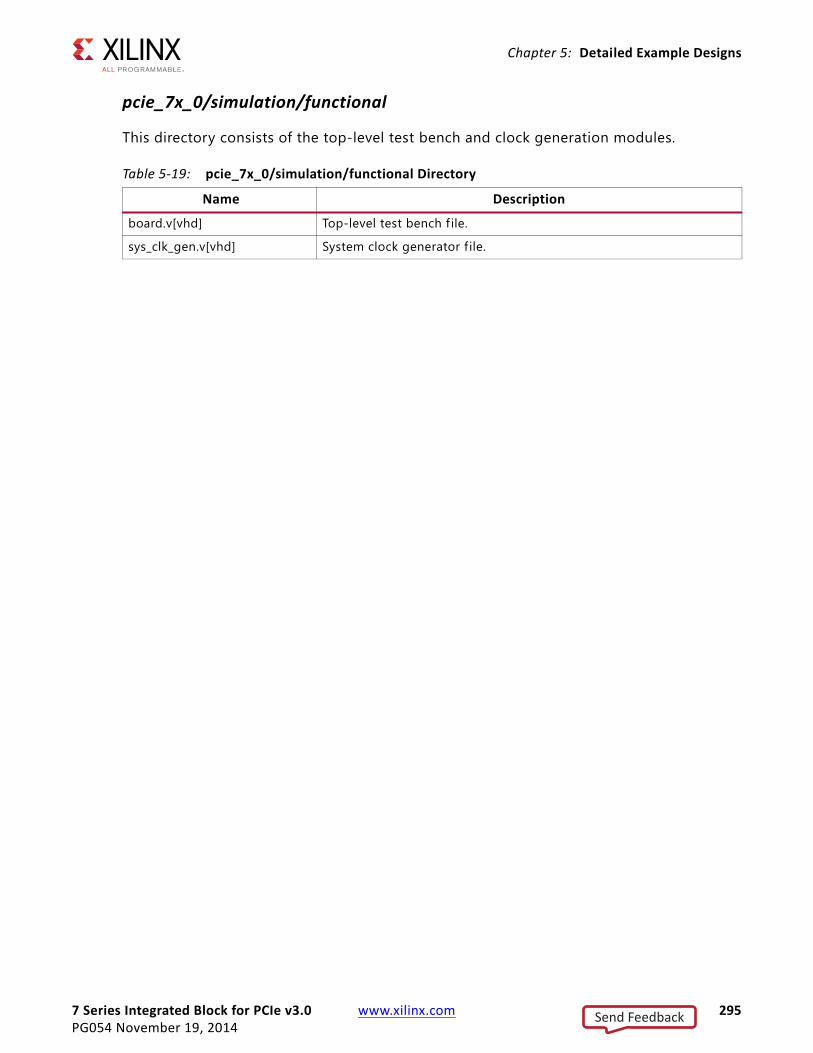
7 Series Integrated Block for PCIe v3.0 www.xilinx.com 295PG054 November 19, 2014
Chapter 5: Detailed Example Designs
pcie_7x_0/simulation/functional
This directory consists of the top-level test bench and clock generation modules.
Table 5-19: pcie_7x_0/simulation/functional Directory
Name Description
board.v[vhd] Top-level test bench f ile.
sys_clk_gen.v[vhd] System clock generator f ile.
Send Feedback

7 Series Integrated Block for PCIe v3.0 www.xilinx.com 296PG054 November 19, 2014
Chapter 6
Test BenchesThis chapter contains information about the test benches provided in the Vivado® Design Suite environment.
Root Port Model Test Bench for EndpointThe PCI Express Root Port Model is a robust test bench environment that provides a test program interface that can be used with the provided PIO design or with a user design. The purpose of the Root Port Model is to provide a source mechanism for generating downstream PCI Express TLP traff ic to stimulate your design, and a destination mechanism for receiving upstream PCI Express TLP traff ic from your design in a simulation environment.
Source code for the Root Port Model is included to provide the model for a starting point for your test bench. All the signif icant work for initializing configuration space, creating TLP transactions, generating TLP logs, and providing an interface for creating and verifying tests are complete, allowing you to dedicate efforts to verifying the correct functionality of the design rather than spending time developing an Endpoint core test bench infrastructure.
The Root Port Model consists of:
• Test Programming Interface (TPI), which allows you to stimulate the Endpoint device for the model
• Example tests that illustrate how to use the test program TPI.
• Verilog or VHDL source code for all Root Port Model components, which allow you to customize the test bench.
Figure 6-1 illustrates the Root Port Model coupled with the PIO design.
Send Feedback
7 Series Integrated Block for PCIe v3.0 www.xilinx.com 297PG054 November 19, 2014
Chapter 6: Test Benches
ArchitectureThe Root Port Model consists of these blocks, illustrated in Figure 6-1:
• dsport (Root Port)
• usrapp_tx
• usrapp_rx
• usrapp_com (Verilog only)
The usrapp_tx and usrapp_rx blocks interface with the dsport block for transmission and reception of TLPs to/from the Endpoint Design Under Test (DUT). The Endpoint DUT consists of the Endpoint for PCIe and the PIO design (displayed) or customer design.
X-Ref Target - Figure 6-1
Figure 6-1: Root Port Model and Top-Level Endpoint
TestProgram
Endpoint DUT for PCI Express
PCI Express Fabric
Endpoint Core forPCI Express
PIODesign
dsport
usrapp_tx
usrapp_com
usrapp_rx
OutputLogs
Root Port Model TPI forPCI Express
Send Feedback
7 Series Integrated Block for PCIe v3.0 www.xilinx.com 298PG054 November 19, 2014
Chapter 6: Test Benches
The usrapp_tx block sends TLPs to the dsport block for transmission across the PCI Express Link to the Endpoint DUT. In turn, the Endpoint DUT device transmits TLPs across the PCI Express Link to the dsport block, which are subsequently passed to the usrapp_rx block. The dsport and core are responsible for the data link layer and physical link layer processing when communicating across the PCI Express logic. Both usrapp_tx and usrapp_rx utilize the usrapp_com block for shared functions, for example, TLP processing and log f ile outputting. Transaction sequences or test programs are initiated by the usrapp_tx block to stimulate the logic interface of the Endpoint device. TLP responses from the Endpoint device are received by the usrapp_rx block. Communication between the usrapp_tx and usrapp_rx blocks allow the usrapp_tx block to verify correct behavior and act accordingly when the usrapp_rx block has received TLPs from the Endpoint device.
Simulating the Example DesignTo simulate the design, see Simulating the Example Design, page 284.
Scaled Simulation TimeoutsThe simulation model of the 7 Series FPGAs Integrated Block for PCI Express uses scaled down times during link training to allow for the link to train in a reasonable amount of time during simulation. According to the PCI Express Specification, rev. 2.1 [Ref 2], there are various timeouts associated with the link training and status state machine (LTSSM) states. The 7 series FPGAs integrated block scales these timeouts by a factor of 256 in simulation, except in the Recovery Speed_1 LTSSM state, where the timeouts are not scaled.
Test SelectionTable 6-1 describes the tests provided with the Root Port Model, followed by specif ic sections for VHDL and Verilog test selection.
Table 6-1: Root Port Model Provided Tests
Test Name Test in VHDL/Verilog Description
sample_smoke_test0 Verilog and VHDL
Issues a PCI Type 0 Configuration Read TLP and waits for the completion TLP; then compares the value returned with the expected Device/Vendor ID value.
sample_smoke_test1 Verilog
Performs the same operation as sample_smoke_test0 but makes use of expectation tasks. This test uses two separate test program threads: • the f irst thread issues the PCI Type 0 Configuration Read TLP, and • the second thread issues the Completion with Data TLP expectation
task. This test illustrates the form for a parallel test that uses expectation tasks. This test form enables for you to confirm the receipt of any TLPs from your design. Additionally, this method can be used to confirm reception of TLPs when ordering is unimportant.
Send Feedback
7 Series Integrated Block for PCIe v3.0 www.xilinx.com 299PG054 November 19, 2014
Chapter 6: Test Benches
Output LoggingWhen a test fails on the example or customer design, the test programmer debugs the offending test case. Typically, the test programmer inspects the wave f ile for the simulation and cross-reference this to the messages displayed on the standard output. Because this approach can be very time consuming, the Root Port Model offers an output logging mechanism to assist the tester with debugging failing test cases to speed the process.
The Root Port Model creates three output log files during each simulation run.
• rx.dat and tx.dat. These log files each contain a detailed record of every TLP that was received and transmitted, respectively, by the Root Port Model. When you understand the expected TLP transmission during a specific test case, you can more easily isolate the failure.
• error.dat. This log f ile is used in conjunction with the expectation tasks. Test programs that use the expectation tasks generate a general error message to standard output. Detailed information about the specif ic comparison failures that have occurred due to the expectation error is located within error.dat.
Parallel Test ProgramsThere are two classes of tests supported by the Root Port Model:
• Sequential tests. Tests that exist within one process and behave similarly to sequential programs. The test depicted in Test Program: pio_writeReadBack_test0, page 301 is an example of a sequential test. Sequential tests are very useful when verifying behavior that have events with a known order.
• Parallel tests. Tests involving more than one process thread. The test sample_smoke_test1 is an example of a parallel test with two process threads. Parallel tests are very useful when verifying that a specif ic set of events have occurred, however the order of these events are not known.
A typical parallel test uses the form of one command thread and one or more expectation threads. These threads work together to verify the device functionality. The role of the command thread is to create the necessary TLP transactions that cause the device to receive and generate TLPs. The role of the expectation threads is to verify the reception of an expected TLP. The Root Port Model TPI has a complete set of expectation tasks to be used in conjunction with parallel tests.
Because the example design is a target-only device, only Completion TLPs can be expected by parallel test programs while using the PIO design. However, the full library of expectation tasks can be used for expecting any TLP type when used in conjunction with the user design (which can include bus-mastering functionality). Currently, the VHDL version of the Root Port Model Test Bench does not support Parallel tests.
Send Feedback
7 Series Integrated Block for PCIe v3.0 www.xilinx.com 300PG054 November 19, 2014
Chapter 6: Test Benches
Test DescriptionThe Root Port Model provides a Test Program Interface (TPI). The TPI provides the means to create tests by invoking a series of Verilog tasks. All Root Port Model tests should follow the same six steps:
1. Perform conditional comparison of a unique test name.
2. Set up master timeout in case simulation hangs.
3. Wait for Reset and link-up.
4. Initialize the configuration space of the Endpoint.
5. Transmit and receive TLPs between the Root Port Model and the Endpoint DUT.
6. Verify that the test succeeded.
Send Feedback
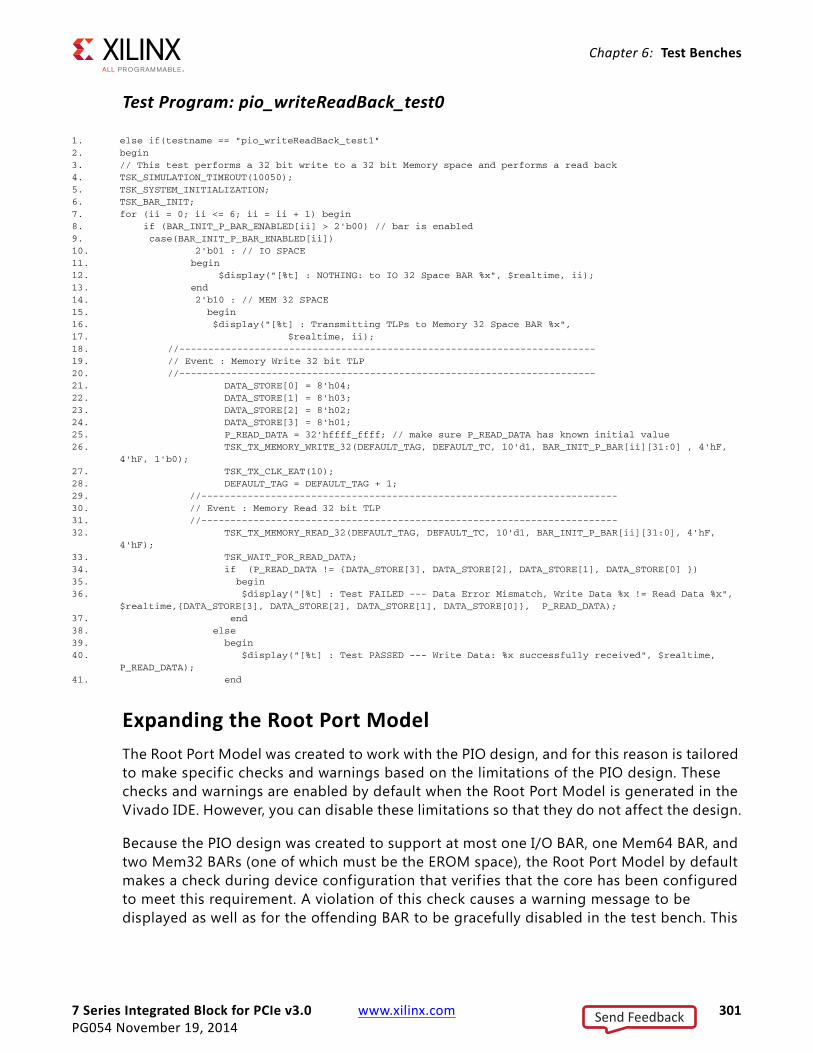
7 Series Integrated Block for PCIe v3.0 www.xilinx.com 301PG054 November 19, 2014
Chapter 6: Test Benches
Test Program: pio_writeReadBack_test0
Expanding the Root Port ModelThe Root Port Model was created to work with the PIO design, and for this reason is tailored to make specif ic checks and warnings based on the limitations of the PIO design. These checks and warnings are enabled by default when the Root Port Model is generated in the Vivado IDE. However, you can disable these limitations so that they do not affect the design.
Because the PIO design was created to support at most one I/O BAR, one Mem64 BAR, and two Mem32 BARs (one of which must be the EROM space), the Root Port Model by default makes a check during device configuration that verif ies that the core has been configured to meet this requirement. A violation of this check causes a warning message to be displayed as well as for the offending BAR to be gracefully disabled in the test bench. This
1. else if(testname == "pio_writeReadBack_test1"2. begin3. // This test performs a 32 bit write to a 32 bit Memory space and performs a read back4. TSK_SIMULATION_TIMEOUT(10050);5. TSK_SYSTEM_INITIALIZATION;6. TSK_BAR_INIT;7. for (ii = 0; ii <= 6; ii = ii + 1) begin 8. if (BAR_INIT_P_BAR_ENABLED[ii] > 2'b00) // bar is enabled 9. case(BAR_INIT_P_BAR_ENABLED[ii])10. 2'b01 : // IO SPACE11. begin 12. $display("[%t] : NOTHING: to IO 32 Space BAR %x", $realtime, ii);13. end 14. 2'b10 : // MEM 32 SPACE15. begin 16. $display("[%t] : Transmitting TLPs to Memory 32 Space BAR %x",17. $realtime, ii);18. //------------------------------------------------------------------------19. // Event : Memory Write 32 bit TLP20. //------------------------------------------------------------------------21. DATA_STORE[0] = 8'h04;22. DATA_STORE[1] = 8'h03;23. DATA_STORE[2] = 8'h02;24. DATA_STORE[3] = 8'h01;25. P_READ_DATA = 32'hffff_ffff; // make sure P_READ_DATA has known initial value 26. TSK_TX_MEMORY_WRITE_32(DEFAULT_TAG, DEFAULT_TC, 10'd1, BAR_INIT_P_BAR[ii][31:0] , 4'hF,
4'hF, 1'b0);27. TSK_TX_CLK_EAT(10);28. DEFAULT_TAG = DEFAULT_TAG + 1;29. //------------------------------------------------------------------------30. // Event : Memory Read 32 bit TLP31. //------------------------------------------------------------------------32. TSK_TX_MEMORY_READ_32(DEFAULT_TAG, DEFAULT_TC, 10'd1, BAR_INIT_P_BAR[ii][31:0], 4'hF,
4'hF);33. TSK_WAIT_FOR_READ_DATA;34. if (P_READ_DATA != {DATA_STORE[3], DATA_STORE[2], DATA_STORE[1], DATA_STORE[0] }) 35. begin36. $display("[%t] : Test FAILED --- Data Error Mismatch, Write Data %x != Read Data %x",
$realtime,{DATA_STORE[3], DATA_STORE[2], DATA_STORE[1], DATA_STORE[0]}, P_READ_DATA);37. end38. else39. begin40. $display("[%t] : Test PASSED --- Write Data: %x successfully received", $realtime,
P_READ_DATA);41. end
Send Feedback
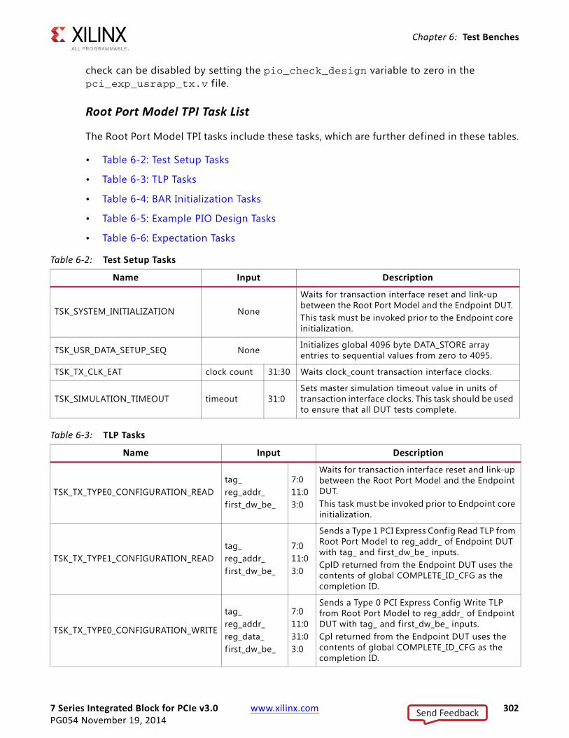
7 Series Integrated Block for PCIe v3.0 www.xilinx.com 302PG054 November 19, 2014
Chapter 6: Test Benches
check can be disabled by setting the pio_check_design variable to zero in the pci_exp_usrapp_tx.v f ile.
Root Port Model TPI Task List
The Root Port Model TPI tasks include these tasks, which are further defined in these tables.
• Table 6-2: Test Setup Tasks
• Table 6-3: TLP Tasks
• Table 6-4: BAR Initialization Tasks
• Table 6-5: Example PIO Design Tasks
• Table 6-6: Expectation Tasks
Table 6-2: Test Setup Tasks
Name Input Description
TSK_SYSTEM_INITIALIZATION None
Waits for transaction interface reset and link-up between the Root Port Model and the Endpoint DUT. This task must be invoked prior to the Endpoint core initialization.
TSK_USR_DATA_SETUP_SEQ None Initializes global 4096 byte DATA_STORE array entries to sequential values from zero to 4095.
TSK_TX_CLK_EAT clock count 31:30 Waits clock_count transaction interface clocks.
TSK_SIMULATION_TIMEOUT timeout 31:0Sets master simulation timeout value in units of transaction interface clocks. This task should be used to ensure that all DUT tests complete.
Table 6-3: TLP Tasks
Name Input Description
TSK_TX_TYPE0_CONFIGURATION_READtag_reg_addr_first_dw_be_
7:011:03:0
Waits for transaction interface reset and link-up between the Root Port Model and the Endpoint DUT. This task must be invoked prior to Endpoint core initialization.
TSK_TX_TYPE1_CONFIGURATION_READtag_reg_addr_first_dw_be_
7:011:03:0
Sends a Type 1 PCI Express Config Read TLP from Root Port Model to reg_addr_ of Endpoint DUT with tag_ and f irst_dw_be_ inputs. CplD returned from the Endpoint DUT uses the contents of global COMPLETE_ID_CFG as the completion ID.
TSK_TX_TYPE0_CONFIGURATION_WRITE
tag_reg_addr_reg_data_first_dw_be_
7:011:031:03:0
Sends a Type 0 PCI Express Config Write TLP from Root Port Model to reg_addr_ of Endpoint DUT with tag_ and f irst_dw_be_ inputs. Cpl returned from the Endpoint DUT uses the contents of global COMPLETE_ID_CFG as the completion ID.
Send Feedback

7 Series Integrated Block for PCIe v3.0 www.xilinx.com 303PG054 November 19, 2014
Chapter 6: Test Benches
TSK_TX_TYPE1_CONFIGURATION_WRITE
tag_reg_addr_reg_data_first_dw_be_
7:011:031:03:0
Sends a Type 1 PCI Express Config Write TLP from Root Port Model to reg_addr_ of Endpoint DUT with tag_ and f irst_dw_be_ inputs. Cpl returned from the Endpoint DUT uses the contents of global COMPLETE_ID_CFG as the completion ID.
TSK_TX_MEMORY_READ_32
tag_tc_len_addr_last_dw_be_first_dw_be_
7:02:09:031:03:03:0
Sends a PCI Express Memory Read TLP from Root Port to 32-bit memory address addr_ of Endpoint DUT.CplD returned from the Endpoint DUT uses the contents of global COMPLETE_ID_CFG as the completion ID.
TSK_TX_MEMORY_READ_64
tag_tc_len_addr_last_dw_be_first_dw_be_
7:02:09:063:03:03:0
Sends a PCI Express Memory Read TLP from Root Port Model to 64-bit memory address addr_ of Endpoint DUT.CplD returned from the Endpoint DUT uses the contents of global COMPLETE_ID_CFG as the completion ID.
TSK_TX_MEMORY_WRITE_32
tag_tc_len_addr_last_dw_be_first_dw_be_ep_
7:02:09:031:03:03:0–
Sends a PCI Express Memory Write TLP from Root Port Model to 32-bit memory address addr_ of Endpoint DUT.CplD returned from the Endpoint DUT uses the contents of global COMPLETE_ID_CFG as the completion ID.The global DATA_STORE byte array is used to pass write data to task.
TSK_TX_MEMORY_WRITE_64
tag_tc_len_addr_last_dw_be_first_dw_be_ep_
7:02:09:063:03:03:0–
Sends a PCI Express Memory Write TLP from Root Port Model to 64-bit memory address addr_ of Endpoint DUT. CplD returned from the Endpoint DUT uses the contents of global COMPLETE_ID_CFG as the completion ID.The global DATA_STORE byte array is used to pass write data to task.
TSK_TX_COMPLETION
tag_tc_len_comp_status_
7:02:09:02:0
Sends a PCI Express Completion TLP from Root Port Model to the Endpoint DUT using global COMPLETE_ID_CFG as the completion ID.
TSK_TX_COMPLETION_DATA
tag_tc_len_byte_countlower_addrcomp_statusep_
7:02:09:011:06:02:0–
Sends a PCI Express Completion with Data TLP from Root Port Model to the Endpoint DUT using global COMPLETE_ID_CFG as the completion ID.The global DATA_STORE byte array is used to pass completion data to task.
Table 6-3: TLP Tasks (Cont’d)
Name Input Description
Send Feedback
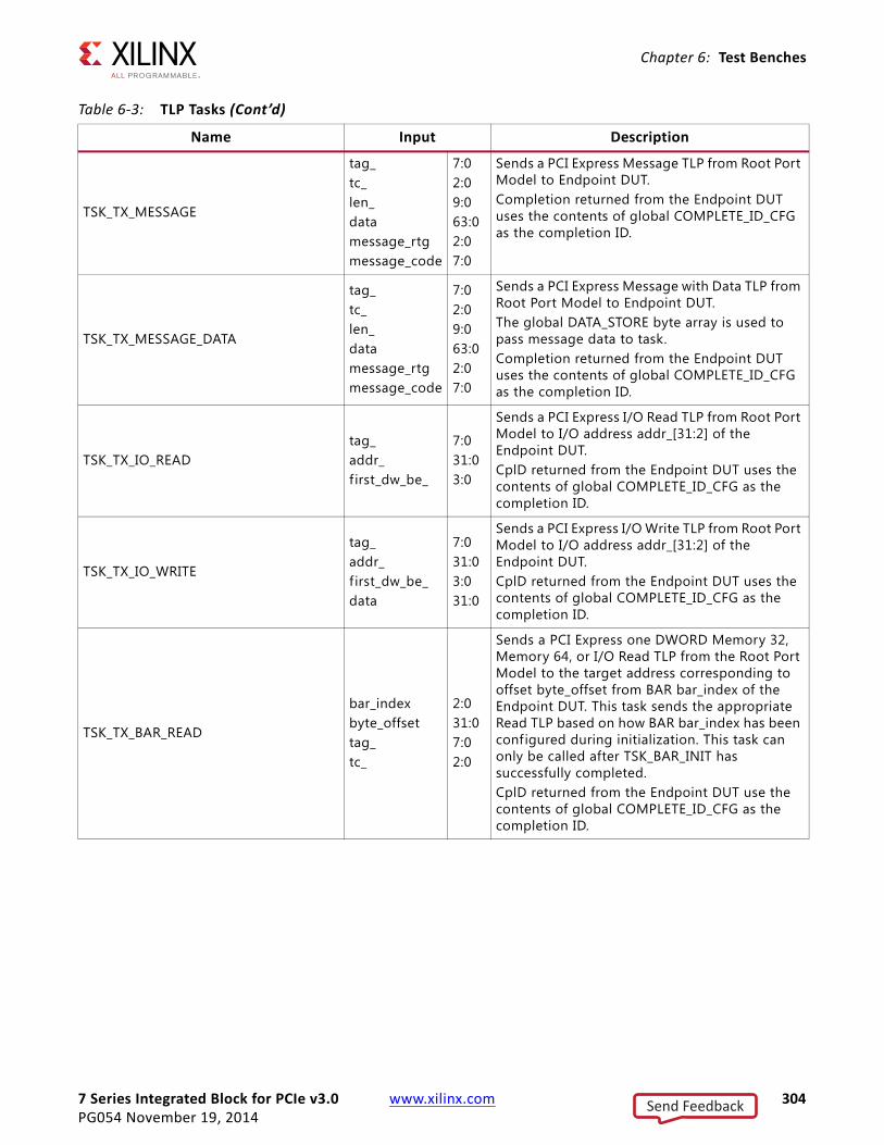
7 Series Integrated Block for PCIe v3.0 www.xilinx.com 304PG054 November 19, 2014
Chapter 6: Test Benches
TSK_TX_MESSAGE
tag_tc_len_datamessage_rtgmessage_code
7:02:09:063:02:07:0
Sends a PCI Express Message TLP from Root Port Model to Endpoint DUT.Completion returned from the Endpoint DUT uses the contents of global COMPLETE_ID_CFG as the completion ID.
TSK_TX_MESSAGE_DATA
tag_tc_len_datamessage_rtgmessage_code
7:02:09:063:02:07:0
Sends a PCI Express Message with Data TLP from Root Port Model to Endpoint DUT.The global DATA_STORE byte array is used to pass message data to task.Completion returned from the Endpoint DUT uses the contents of global COMPLETE_ID_CFG as the completion ID.
TSK_TX_IO_READtag_addr_first_dw_be_
7:031:03:0
Sends a PCI Express I/O Read TLP from Root Port Model to I/O address addr_[31:2] of the Endpoint DUT.CplD returned from the Endpoint DUT uses the contents of global COMPLETE_ID_CFG as the completion ID.
TSK_TX_IO_WRITE
tag_addr_first_dw_be_data
7:031:03:031:0
Sends a PCI Express I/O Write TLP from Root Port Model to I/O address addr_[31:2] of the Endpoint DUT.CplD returned from the Endpoint DUT uses the contents of global COMPLETE_ID_CFG as the completion ID.
TSK_TX_BAR_READ
bar_indexbyte_offsettag_tc_
2:031:07:02:0
Sends a PCI Express one DWORD Memory 32, Memory 64, or I/O Read TLP from the Root Port Model to the target address corresponding to offset byte_offset from BAR bar_index of the Endpoint DUT. This task sends the appropriate Read TLP based on how BAR bar_index has been configured during initialization. This task can only be called after TSK_BAR_INIT has successfully completed.CplD returned from the Endpoint DUT use the contents of global COMPLETE_ID_CFG as the completion ID.
Table 6-3: TLP Tasks (Cont’d)
Name Input Description
Send Feedback
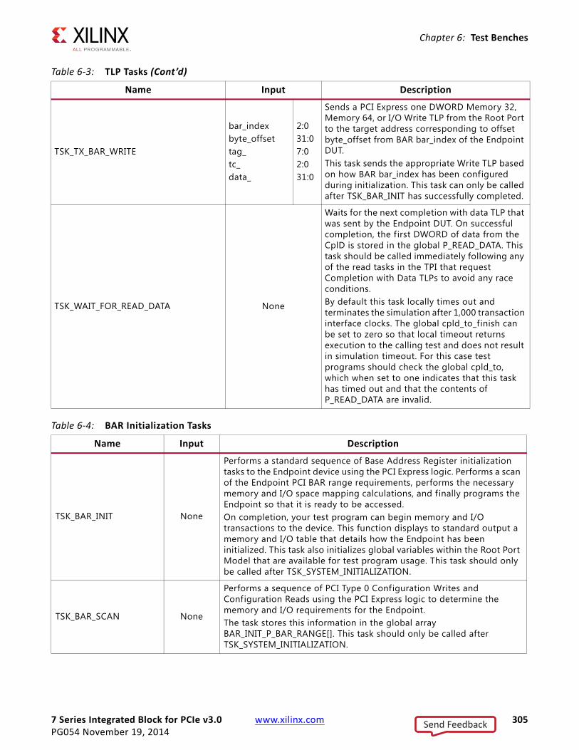
7 Series Integrated Block for PCIe v3.0 www.xilinx.com 305PG054 November 19, 2014
Chapter 6: Test Benches
TSK_TX_BAR_WRITE
bar_indexbyte_offsettag_tc_data_
2:031:07:02:031:0
Sends a PCI Express one DWORD Memory 32, Memory 64, or I/O Write TLP from the Root Port to the target address corresponding to offset byte_offset from BAR bar_index of the Endpoint DUT. This task sends the appropriate Write TLP based on how BAR bar_index has been configured during initialization. This task can only be called after TSK_BAR_INIT has successfully completed.
TSK_WAIT_FOR_READ_DATA None
Waits for the next completion with data TLP that was sent by the Endpoint DUT. On successful completion, the first DWORD of data from the CplD is stored in the global P_READ_DATA. This task should be called immediately following any of the read tasks in the TPI that request Completion with Data TLPs to avoid any race conditions.By default this task locally times out and terminates the simulation after 1,000 transaction interface clocks. The global cpld_to_finish can be set to zero so that local timeout returns execution to the calling test and does not result in simulation timeout. For this case test programs should check the global cpld_to, which when set to one indicates that this task has timed out and that the contents of P_READ_DATA are invalid.
Table 6-3: TLP Tasks (Cont’d)
Name Input Description
Table 6-4: BAR Initialization Tasks
Name Input Description
TSK_BAR_INIT None
Performs a standard sequence of Base Address Register initialization tasks to the Endpoint device using the PCI Express logic. Performs a scan of the Endpoint PCI BAR range requirements, performs the necessary memory and I/O space mapping calculations, and f inally programs the Endpoint so that it is ready to be accessed. On completion, your test program can begin memory and I/O transactions to the device. This function displays to standard output a memory and I/O table that details how the Endpoint has been initialized. This task also initializes global variables within the Root Port Model that are available for test program usage. This task should only be called after TSK_SYSTEM_INITIALIZATION.
TSK_BAR_SCAN None
Performs a sequence of PCI Type 0 Configuration Writes and Configuration Reads using the PCI Express logic to determine the memory and I/O requirements for the Endpoint. The task stores this information in the global array BAR_INIT_P_BAR_RANGE[]. This task should only be called after TSK_SYSTEM_INITIALIZATION.
Send Feedback

7 Series Integrated Block for PCIe v3.0 www.xilinx.com 306PG054 November 19, 2014
Chapter 6: Test Benches
TSK_BUILD_PCIE_MAP None
Performs memory and I/O mapping algorithm and allocates Memory 32, Memory 64, and I/O space based on the Endpoint requirements. This task has been customized to work in conjunction with the limitations of the PIO design and should only be called after completion of TSK_BAR_SCAN.
TSK_DISPLAY_PCIE_MAP None
Displays the memory mapping information of the Endpoint core PCI Base Address Registers. For each BAR, the BAR value, the BAR range, and BAR type is given. This task should only be called after completion of TSK_BUILD_PCIE_MAP.
Table 6-4: BAR Initialization Tasks (Cont’d)
Name Input Description
Table 6-5: Example PIO Design Tasks
Name Input Description
TSK_TX_READBACK_CONFIG None
Performs a sequence of PCI Type 0 Configuration Reads to the Endpoint device Base Address Registers, PCI Command Register, and PCIe Device Control Register using the PCI Express logic. This task should only be called after TSK_SYSTEM_INITIALIZATION.
TSK_MEM_TEST_DATA_BUS bar_index 2:0
Tests whether the PIO design FPGA block RAM data bus interface is correctly connected by performing a 32-bit walking ones data test to the I/O or memory address pointed to by the input bar_index. For an exhaustive test, this task should be called four times, once for each block RAM used in the PIO design.
TSK_MEM_TEST_ADDR_BUSbar_indexnBytes
2:031:0
Tests whether the PIO design FPGA block RAM address bus interface is accurately connected by performing a walking ones address test starting at the I/O or memory address pointed to by the input bar_index. For an exhaustive test, this task should be called four times, once for each block RAM used in the PIO design. Also, the nBytes input should specify the entire size of the individual block RAM.
TSK_MEM_TEST_DEVICEbar_indexnBytes
2:031:0
Tests the integrity of each bit of the PIO design FPGA block RAM by performing an increment/decrement test on all bits starting at the block RAM pointed to by the input bar_index with the range specified by input nBytes. For an exhaustive test, this task should be called four times, once for each block RAM used in the PIO design. Also, the nBytes input should specify the entire size of the individual block RAM.
Send Feedback
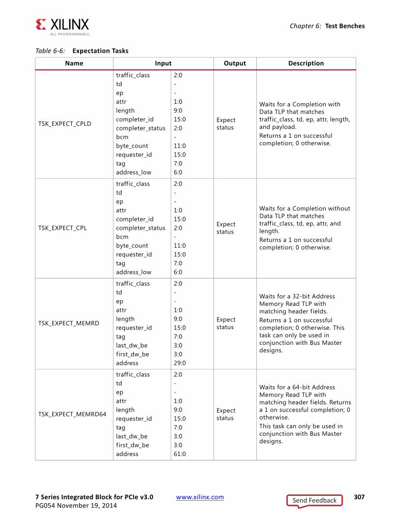
7 Series Integrated Block for PCIe v3.0 www.xilinx.com 307PG054 November 19, 2014
Chapter 6: Test Benches
Table 6-6: Expectation Tasks
Name Input Output Description
TSK_EXPECT_CPLD
traff ic_classtdepattrlengthcompleter_idcompleter_statusbcmbyte_countrequester_idtagaddress_low
2:0--1:09:015:02:0-11:015:07:06:0
Expect status
Waits for a Completion with Data TLP that matches traffic_class, td, ep, attr, length, and payload. Returns a 1 on successful completion; 0 otherwise.
TSK_EXPECT_CPL
traff ic_classtdepattrcompleter_idcompleter_statusbcmbyte_countrequester_idtagaddress_low
2:0--1:015:02:0-11:015:07:06:0
Expect status
Waits for a Completion without Data TLP that matches traffic_class, td, ep, attr, and length. Returns a 1 on successful completion; 0 otherwise.
TSK_EXPECT_MEMRD
traff ic_classtdepattrlengthrequester_idtaglast_dw_befirst_dw_beaddress
2:0--1:09:015:07:03:03:029:0
Expect status
Waits for a 32-bit Address Memory Read TLP with matching header f ields. Returns a 1 on successful completion; 0 otherwise. This task can only be used in conjunction with Bus Master designs.
TSK_EXPECT_MEMRD64
traff ic_classtdepattrlengthrequester_idtaglast_dw_befirst_dw_beaddress
2:0--1:09:015:07:03:03:061:0
Expect status
Waits for a 64-bit Address Memory Read TLP with matching header fields. Returns a 1 on successful completion; 0 otherwise. This task can only be used in conjunction with Bus Master designs.
Send Feedback
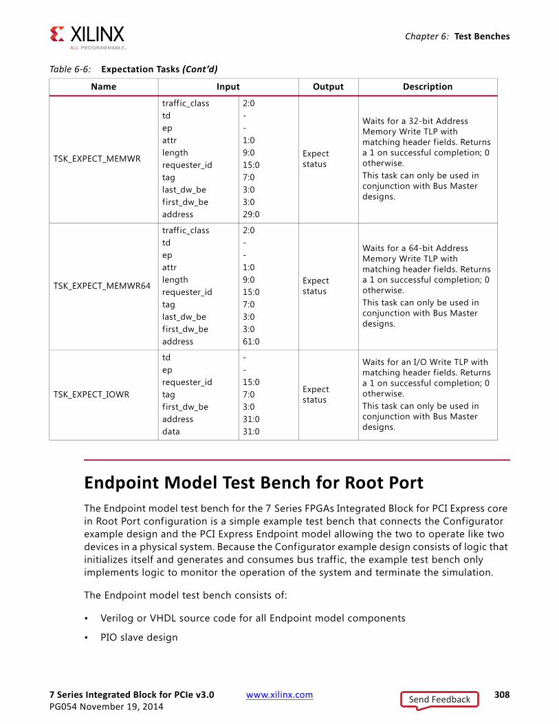
7 Series Integrated Block for PCIe v3.0 www.xilinx.com 308PG054 November 19, 2014
Chapter 6: Test Benches
Endpoint Model Test Bench for Root PortThe Endpoint model test bench for the 7 Series FPGAs Integrated Block for PCI Express core in Root Port configuration is a simple example test bench that connects the Configurator example design and the PCI Express Endpoint model allowing the two to operate like two devices in a physical system. Because the Configurator example design consists of logic that initializes itself and generates and consumes bus traff ic, the example test bench only implements logic to monitor the operation of the system and terminate the simulation.
The Endpoint model test bench consists of:
• Verilog or VHDL source code for all Endpoint model components
• PIO slave design
TSK_EXPECT_MEMWR
traff ic_classtdepattrlengthrequester_idtaglast_dw_befirst_dw_beaddress
2:0--1:09:015:07:03:03:029:0
Expect status
Waits for a 32-bit Address Memory Write TLP with matching header fields. Returns a 1 on successful completion; 0 otherwise. This task can only be used in conjunction with Bus Master designs.
TSK_EXPECT_MEMWR64
traff ic_classtdepattrlengthrequester_idtaglast_dw_befirst_dw_beaddress
2:0--1:09:015:07:03:03:061:0
Expect status
Waits for a 64-bit Address Memory Write TLP with matching header fields. Returns a 1 on successful completion; 0 otherwise. This task can only be used in conjunction with Bus Master designs.
TSK_EXPECT_IOWR
tdeprequester_idtagfirst_dw_beaddressdata
--15:07:03:031:031:0
Expect status
Waits for an I/O Write TLP with matching header fields. Returns a 1 on successful completion; 0 otherwise.This task can only be used in conjunction with Bus Master designs.
Table 6-6: Expectation Tasks (Cont’d)
Name Input Output Description
Send Feedback

7 Series Integrated Block for PCIe v3.0 www.xilinx.com 309PG054 November 19, 2014
Chapter 6: Test Benches
Figure 5-13, page 277 illustrates the Endpoint model coupled with the Configurator example design.
ArchitectureThe Endpoint model consists of these blocks:
• PCI Express Endpoint (7 Series FPGAs Integrated Block for PCI Express in Endpoint configuration) model.
• PIO slave design, consisting of:
° PIO_RX_ENGINE
° PIO_TX_ENGINE
° PIO_EP_MEM
° PIO_TO_CTRL
The PIO_RX_ENGINE and PIO_TX_ENGINE blocks interface with the ep block for reception and transmission of TLPs from/to the Root Port Design Under Test (DUT). The Root Port DUT consists of the core configured as a Root Port and the Configurator Example Design, which consists of a Configurator block and a PIO Master design, or customer design.
The PIO slave design is described in detail in Programmed Input/Output: Endpoint Example Design, page 261.
Simulating the Example DesignTo simulate the design, see Simulating the Example Design, page 284.
Note: For Cadence IES, the work construct DEFINE WORK WORK must be inserted manually into the cds.lib f ile.
Scaled Simulation TimeoutsThe simulation model of the core uses scaled down times during link training to allow for the link to train in a reasonable amount of time during simulation. According to the PCI Express Specification, rev. 2.1 [Ref 2], there are various timeouts associated with the link training and status state machine (LTSSM) states. The core scales these timeouts by a factor of 256 in simulation, except in the Recovery Speed_1 LTSSM state, where the timeouts are not scaled.
Send Feedback
7 Series Integrated Block for PCIe v3.0 www.xilinx.com 310PG054 November 19, 2014
Chapter 6: Test Benches
Output LoggingThe test bench outputs messages, captured in the simulation log, indicating the time at which these occur:
• user_reset is deasserted
• user_lnk_up is asserted
• cfg_done is asserted by the Configurator
• pio_test_finished is asserted by the PIO Master
• Simulation Timeout (if pio_test_finished or pio_test_failed is never asserted)
Send Feedback

7 Series Integrated Block for PCIe v3.0 www.xilinx.com 311PG054 November 19, 2014
Appendix A
Migrating and UpgradingThis appendix contains information about migrating a design from ISE® Design Suite to the Vivado® Design Suite, and for upgrading to a more recent version of the IP core. For customers upgrading in the Vivado Design Suite, important details (where applicable) about any port changes and other impact to user logic are included.
Migrating to the Vivado Design SuiteThis section covers:
• Migration to 7 Series Devices
• TRN to AXI Migration Considerations
For information on migrating to the Vivado Design Suite, see ISE to Vivado Design Suite Migration Methodology Guide (UG911)[Ref 17].
Migration to 7 Series DevicesFor migrating to the 7 Series FPGAs Integrated Block for PCI Express® from the Virtex®-6 FPGA Integrated Block for PCI Express, the list in this section describes the differences in behaviors and options between the 7 Series FPGAs Integrated Block for PCI Express core and the Virtex-6 FPGA Integrated Block for PCI Express core, version v2.x with the AXI4-Stream interface.
Core Capability Differences
• 8-Lane, 5.0 Gb/s (Gen2) Speed Operation for Root Port Configuration: The 7 Series FPGAs Integrated Block for PCI Express also supports the 5.0 Gb/s speed operation for the 8-lane Root Port Configuration.
• 128-bit Interface: The 7 Series Integrated Block for PCIe supports the 128-bit interface for the 8-lane, 2.5 Gb/s configuration and 4-lane, 5.0 Gb/s configuration.
Configuration Interface
Table A-1 lists the Configuration interface signals whose names were changed.
Send Feedback
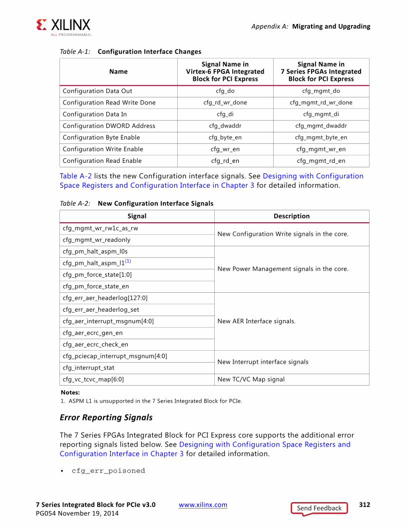
7 Series Integrated Block for PCIe v3.0 www.xilinx.com 312PG054 November 19, 2014
Appendix A: Migrating and Upgrading
Table A-2 lists the new Configuration interface signals. See Designing with Configuration Space Registers and Configuration Interface in Chapter 3 for detailed information.
Error Reporting Signals
The 7 Series FPGAs Integrated Block for PCI Express core supports the additional error reporting signals listed below. See Designing with Configuration Space Registers and Configuration Interface in Chapter 3 for detailed information.
• cfg_err_poisoned
Table A-1: Configuration Interface Changes
NameSignal Name in
Virtex-6 FPGA Integrated Block for PCI Express
Signal Name in 7 Series FPGAs Integrated
Block for PCI Express
Configuration Data Out cfg_do cfg_mgmt_do
Configuration Read Write Done cfg_rd_wr_done cfg_mgmt_rd_wr_done
Configuration Data In cfg_di cfg_mgmt_di
Configuration DWORD Address cfg_dwaddr cfg_mgmt_dwaddr
Configuration Byte Enable cfg_byte_en cfg_mgmt_byte_en
Configuration Write Enable cfg_wr_en cfg_mgmt_wr_en
Configuration Read Enable cfg_rd_en cfg_mgmt_rd_en
Table A-2: New Configuration Interface Signals
Signal Description
cfg_mgmt_wr_rw1c_as_rwNew Configuration Write signals in the core.
cfg_mgmt_wr_readonly
cfg_pm_halt_aspm_l0s
New Power Management signals in the core.cfg_pm_halt_aspm_l1(1)
cfg_pm_force_state[1:0]
cfg_pm_force_state_en
cfg_err_aer_headerlog[127:0]
New AER Interface signals.
cfg_err_aer_headerlog_set
cfg_aer_interrupt_msgnum[4:0]
cfg_aer_ecrc_gen_en
cfg_aer_ecrc_check_en
cfg_pciecap_interrupt_msgnum[4:0]New Interrupt interface signals
cfg_interrupt_stat
cfg_vc_tcvc_map[6:0] New TC/VC Map signal
Notes: 1. ASPM L1 is unsupported in the 7 Series Integrated Block for PCIe.
Send Feedback
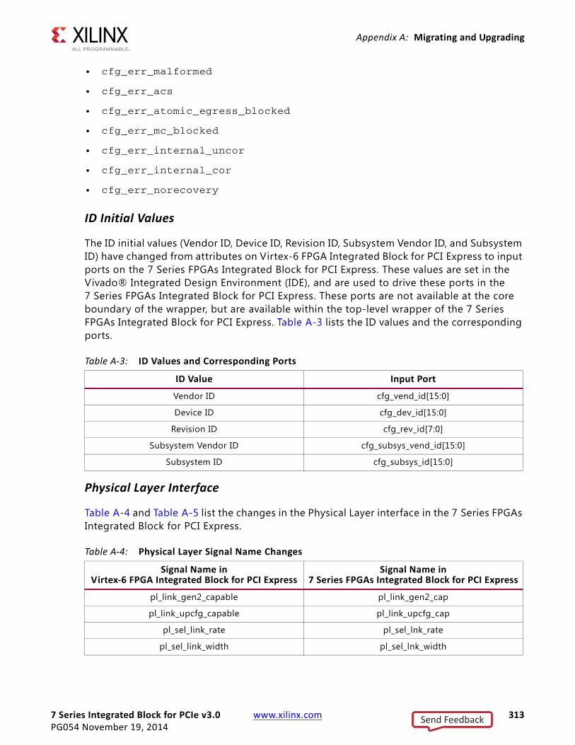
7 Series Integrated Block for PCIe v3.0 www.xilinx.com 313PG054 November 19, 2014
Appendix A: Migrating and Upgrading
• cfg_err_malformed
• cfg_err_acs
• cfg_err_atomic_egress_blocked
• cfg_err_mc_blocked
• cfg_err_internal_uncor
• cfg_err_internal_cor
• cfg_err_norecovery
ID Initial Values
The ID initial values (Vendor ID, Device ID, Revision ID, Subsystem Vendor ID, and Subsystem ID) have changed from attributes on Virtex-6 FPGA Integrated Block for PCI Express to input ports on the 7 Series FPGAs Integrated Block for PCI Express. These values are set in the Vivado® Integrated Design Environment (IDE), and are used to drive these ports in the 7 Series FPGAs Integrated Block for PCI Express. These ports are not available at the core boundary of the wrapper, but are available within the top-level wrapper of the 7 Series FPGAs Integrated Block for PCI Express. Table A-3 lists the ID values and the corresponding ports.
Physical Layer Interface
Table A-4 and Table A-5 list the changes in the Physical Layer interface in the 7 Series FPGAs Integrated Block for PCI Express.
Table A-3: ID Values and Corresponding Ports
ID Value Input Port
Vendor ID cfg_vend_id[15:0]
Device ID cfg_dev_id[15:0]
Revision ID cfg_rev_id[7:0]
Subsystem Vendor ID cfg_subsys_vend_id[15:0]
Subsystem ID cfg_subsys_id[15:0]
Table A-4: Physical Layer Signal Name Changes
Signal Name in Virtex-6 FPGA Integrated Block for PCI Express
Signal Name in7 Series FPGAs Integrated Block for PCI Express
pl_link_gen2_capable pl_link_gen2_cap
pl_link_upcfg_capable pl_link_upcfg_cap
pl_sel_link_rate pl_sel_lnk_rate
pl_sel_link_width pl_sel_lnk_width
Send Feedback
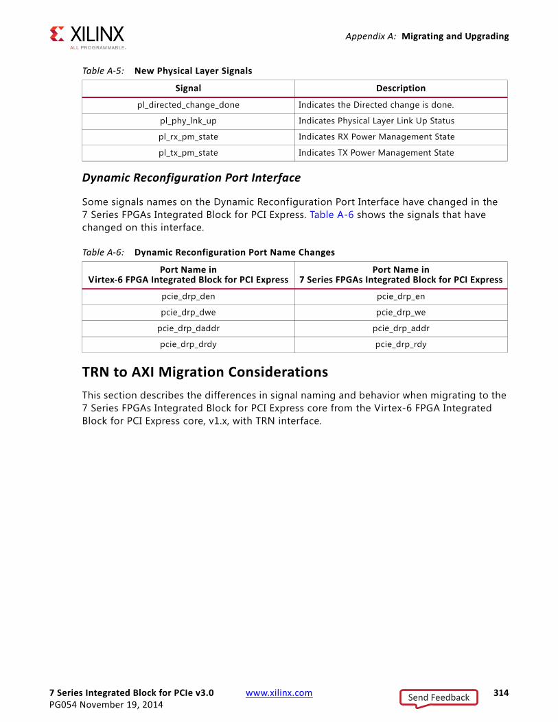
7 Series Integrated Block for PCIe v3.0 www.xilinx.com 314PG054 November 19, 2014
Appendix A: Migrating and Upgrading
Dynamic Reconfiguration Port Interface
Some signals names on the Dynamic Reconfiguration Port Interface have changed in the 7 Series FPGAs Integrated Block for PCI Express. Table A-6 shows the signals that have changed on this interface.
TRN to AXI Migration ConsiderationsThis section describes the differences in signal naming and behavior when migrating to the 7 Series FPGAs Integrated Block for PCI Express core from the Virtex-6 FPGA Integrated Block for PCI Express core, v1.x, with TRN interface.
Table A-5: New Physical Layer Signals
Signal Description
pl_directed_change_done Indicates the Directed change is done.
pl_phy_lnk_up Indicates Physical Layer Link Up Status
pl_rx_pm_state Indicates RX Power Management State
pl_tx_pm_state Indicates TX Power Management State
Table A-6: Dynamic Reconfiguration Port Name Changes
Port Name in Virtex-6 FPGA Integrated Block for PCI Express
Port Name in7 Series FPGAs Integrated Block for PCI Express
pcie_drp_den pcie_drp_en
pcie_drp_dwe pcie_drp_we
pcie_drp_daddr pcie_drp_addr
pcie_drp_drdy pcie_drp_rdy
Send Feedback

7 Series Integrated Block for PCIe v3.0 www.xilinx.com 315PG054 November 19, 2014
Appendix A: Migrating and Upgrading
High-Level Summary
The 7 Series FPGAs Integrated Block for PCI Express updates the main user interface from TRN to the standard AXI4-Stream signal naming and behavior. In addition, all control signals that were active-Low have been changed to active-High. This list summarizes the main changes to the core:
• Signal name changes
• Datapath DWORD ordering
• All control signals are active-High
• Start-of-frame (SOF) signaling is implied
• Remainder signals are replaced with Strobe signals
Step-by-Step Migration Guide
This section describes the steps that a user should take to migrate an existing user application based on TRN to the AXI4-Stream interface.
1. For each signal in Table A-7 labeled “Name change only”, connect the appropriate user application signal to the newly named core signal.
2. For each signal in Table A-7 labeled “Name change; Polarity”, add an inverter and connect the appropriate user application signal to the newly named core signal.
3. Swap the DWORD ordering on the datapath signals as described in Datapath DWORD Ordering.
4. Leave disconnected the user application signal originally connected to trn_tsof_n.
5. Recreate trn_rsof_n as described in the Start-Of-Frame Signaling section and connect to the user application as was originally connected.
6. Make the necessary changes as described in the Remainder/Strobe Signaling section.
7. If using the trn_rsrc_dsc_n signal in the original design, make the changes as described in Packet Transfer Discontinue on Receive section, otherwise leave disconnected.
8. Make the changes as described in the Packet Re-ordering on Receive section.
Send Feedback

7 Series Integrated Block for PCIe v3.0 www.xilinx.com 316PG054 November 19, 2014
Appendix A: Migrating and Upgrading
Signal Changes
Table A-7 details the main differences in signaling between TRN local-link to AXI4-Stream.
Table A-7: Interface Changes
TRN Name AXI4-Stream Name Difference
Common Interface
sys_reset_n sys_rst_n No change
trn_clk user_clk_out Name change
trn_reset_n user_reset_out Name change; Polarity
trn_lnk_up_n user_lnk_up Name change; Polarity
trn_fc_ph[7:0] fc_ph[7:0] Name change only
trn_fc_pd[11:0] fc_pd[11:0] Name change only
trn_fc_nph[7:0] fc_nph[7:0] Name change only
trn_fc_npd[11:0] fc_npd[11:0] Name change only
trn_fc_cplh[7:0] fc_cplh[7:0] Name change only
trn_fc_cpld[11:0] fc_cpld[11:0] Name change only
trn_fc_sel[2:0] fc_sel[2:0] Name change only
Transmit Interface
trn_tsof_n No equivalent for 32- and 64-bit version (see text)
trn_teof_n s_axis_tx_tlast Name change; Polarity
trn_td[W-1:0](W = 32, 64, or 128)
s_axis_tx_tdata[W-1:0] Name change; DWORD Ordering (see text)
trn_trem_n(64-bit interface)
s_axis_tx_tkeep[7:0] Name change; Functional differences (see text)
trn_trem_n[1:0](128-bit interface)
s_axis_tx_tkeep[15:0] Name change; Functional differences (see text)
trn_tsrc_rdy_n s_axis_tx_tvalid Name change; Polarity
trn_tdst_rdy_n s_axis_tx_tready Name change; Polarity
trn_tsrc_dsc_n s_axis_tx_tuser[3] Name change; Polarity
trn_tbuf_av[5:0] tx_buf_av[5:0] Name Change
trn_terr_drop_n tx_err_drop Name change; Polarity
trn_tstr_n s_axis_tx_tuser[2] Name change; Polarity
trn_tcfg_req_n tx_cfg_req Name change; Polarity
trn_tcfg_gnt_n tx_cfg_gnt Name change; Polarity
trn_terrfwd_n s_axis_tx_tuser[1] Name change; Polarity
Receive Interface
trn_rsof_n No equivalent for 32 and 64-bit versions
Send Feedback
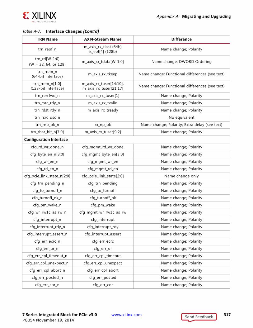
7 Series Integrated Block for PCIe v3.0 www.xilinx.com 317PG054 November 19, 2014
Appendix A: Migrating and Upgrading
trn_reof_n m_axis_rx_tlast (64b)is_eof[4] (128b) Name change; Polarity
trn_rd[W-1:0](W = 32, 64, or 128)
m_axis_rx_tdata[W-1:0] Name change; DWORD Ordering
trn_rrem_n (64-bit interface) m_axis_rx_tkeep Name change; Functional differences (see text)
trn_rrem_n[1:0] (128-bit interface)
m_axis_rx_tuser[14:10], m_axis_rx_tuser[21:17] Name change; Functional differences (see text)
trn_rerrfwd_n m_axis_rx_tuser[1] Name change; Polarity
trn_rsrc_rdy_n m_axis_rx_tvalid Name change; Polarity
trn_rdst_rdy_n m_axis_rx_tready Name change; Polarity
trn_rsrc_dsc_n No equivalent
trn_rnp_ok_n rx_np_ok Name change; Polarity; Extra delay (see text)
trn_rbar_hit_n[7:0] m_axis_rx_tuser[9:2] Name change; Polarity
Configuration Interface
cfg_rd_wr_done_n cfg_mgmt_rd_wr_done Name change; Polarity
cfg_byte_en_n[3:0] cfg_mgmt_byte_en[3:0] Name change; Polarity
cfg_wr_en_n cfg_mgmt_wr_en Name change; Polarity
cfg_rd_en_n cfg_mgmt_rd_en Name change; Polarity
cfg_pcie_link_state_n[2:0] cfg_pcie_link_state[2:0] Name change only
cfg_trn_pending_n cfg_trn_pending Name change; Polarity
cfg_to_turnoff_n cfg_to_turnoff Name change; Polarity
cfg_turnoff_ok_n cfg_turnoff_ok Name change; Polarity
cfg_pm_wake_n cfg_pm_wake Name change; Polarity
cfg_wr_rw1c_as_rw_n cfg_mgmt_wr_rw1c_as_rw Name change; Polarity
cfg_interrupt_n cfg_interrupt Name change; Polarity
cfg_interrupt_rdy_n cfg_interrupt_rdy Name change; Polarity
cfg_interrupt_assert_n cfg_interrupt_assert Name change; Polarity
cfg_err_ecrc_n cfg_err_ecrc Name change; Polarity
cfg_err_ur_n cfg_err_ur Name change; Polarity
cfg_err_cpl_timeout_n cfg_err_cpl_timeout Name change; Polarity
cfg_err_cpl_unexpect_n cfg_err_cpl_unexpect Name change; Polarity
cfg_err_cpl_abort_n cfg_err_cpl_abort Name change; Polarity
cfg_err_posted_n cfg_err_posted Name change; Polarity
cfg_err_cor_n cfg_err_cor Name change; Polarity
Table A-7: Interface Changes (Cont’d)
TRN Name AXI4-Stream Name Difference
Send Feedback

7 Series Integrated Block for PCIe v3.0 www.xilinx.com 318PG054 November 19, 2014
Appendix A: Migrating and Upgrading
Datapath DWORD Ordering
The AXI4-Stream interface swaps the DWORD locations but preserves byte ordering within an individual DWORD as compared to the TRN interface. This change only affects the 64-bit and 128-bit versions of the core. Figure A-1 and Figure A-2 illustrate the DWORD swap ordering from TRN to AXI4-Stream for both 64-bit and 128-bit versions.
For migrating existing 64-bit and 128-bit TRN-based designs, you should swap DWORD locations for the s_axis_tx_tdata[W-1:0] and s_axis_rx_rdata[W-1:0] buses as they enter and exit the core.
For example, existing user application pseudo code:
usr_trn_rd[127:0] = trn_rd[127:0];
should be modif ied to:
usr_trn_rd[127:96] = s_axis_rx_rdata[31:0]usr_trn_rd[95:64] = s_axis_rx_rdata[63:32]usr_trn_rd[63:32] = s_axis_rx_rdata[95:64]usr_trn_rd[31:0] = s_axis_rx_rdata[127:96]
cfg_err_cpl_rdy_n cfg_err_cpl_rdy Name change; Polarity
cfg_err_locked_n cfg_err_locked Name change; Polarity
Table A-7: Interface Changes (Cont’d)
TRN Name AXI4-Stream Name Difference
X-Ref Target - Figure A-1
Figure A-1: TRN vs. AXI DWORD Ordering on Data Bus (64-Bit)X-Ref Target - Figure A-2
Figure A-2: TRN vs. AXI DWORD Ordering on Data Bus (128-Bit)
trn_td[63:0]trn_rd[63:0]
s_axis_tx_tdata[63:0]m_axis_rx_rdata[63:0]
DW0 DW1
DW1 DW0
trn_td[127:0]trn_rd[127:0]
s_axis_tx_tdata[127:0]m_axis_rx_rdata[127:0]
DW0 DW1 DW2 DW3
DW3 DW2 DW1 DW0
Send Feedback
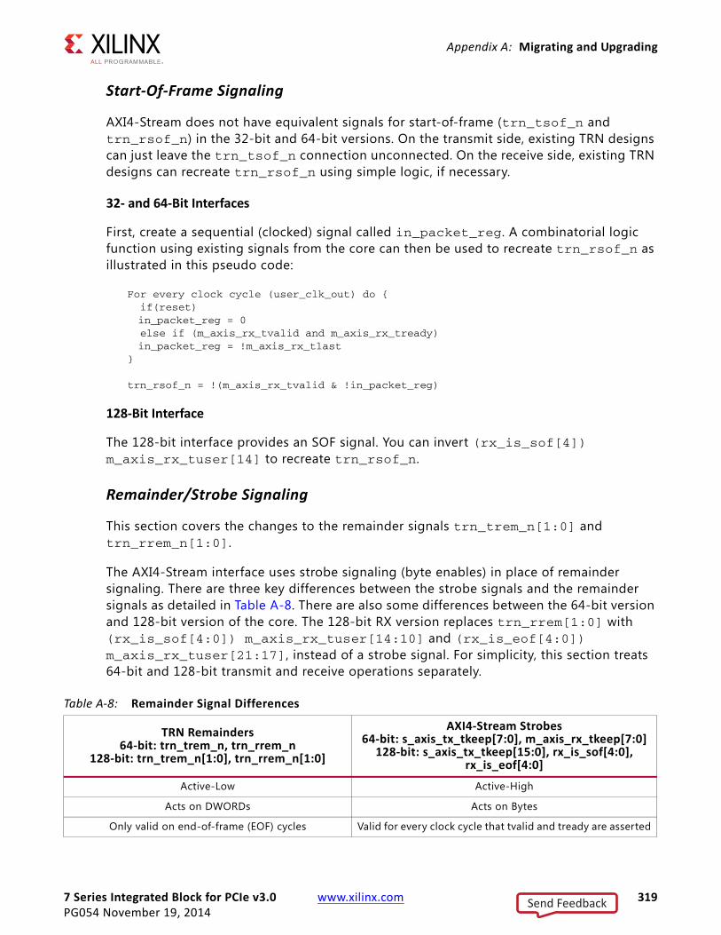
7 Series Integrated Block for PCIe v3.0 www.xilinx.com 319PG054 November 19, 2014
Appendix A: Migrating and Upgrading
Start-Of-Frame Signaling
AXI4-Stream does not have equivalent signals for start-of-frame (trn_tsof_n and trn_rsof_n) in the 32-bit and 64-bit versions. On the transmit side, existing TRN designs can just leave the trn_tsof_n connection unconnected. On the receive side, existing TRN designs can recreate trn_rsof_n using simple logic, if necessary.
32- and 64-Bit Interfaces
First, create a sequential (clocked) signal called in_packet_reg. A combinatorial logic function using existing signals from the core can then be used to recreate trn_rsof_n as illustrated in this pseudo code:
For every clock cycle (user_clk_out) do { if(reset)in_packet_reg = 0
else if (m_axis_rx_tvalid and m_axis_rx_tready)in_packet_reg = !m_axis_rx_tlast
}
trn_rsof_n = !(m_axis_rx_tvalid & !in_packet_reg)
128-Bit Interface
The 128-bit interface provides an SOF signal. You can invert (rx_is_sof[4]) m_axis_rx_tuser[14] to recreate trn_rsof_n.
Remainder/Strobe Signaling
This section covers the changes to the remainder signals trn_trem_n[1:0] and trn_rrem_n[1:0].
The AXI4-Stream interface uses strobe signaling (byte enables) in place of remainder signaling. There are three key differences between the strobe signals and the remainder signals as detailed in Table A-8. There are also some differences between the 64-bit version and 128-bit version of the core. The 128-bit RX version replaces trn_rrem[1:0] with (rx_is_sof[4:0]) m_axis_rx_tuser[14:10] and (rx_is_eof[4:0]) m_axis_rx_tuser[21:17], instead of a strobe signal. For simplicity, this section treats 64-bit and 128-bit transmit and receive operations separately.
Table A-8: Remainder Signal Differences
TRN Remainders64-bit: trn_trem_n, trn_rrem_n
128-bit: trn_trem_n[1:0], trn_rrem_n[1:0]
AXI4-Stream Strobes64-bit: s_axis_tx_tkeep[7:0], m_axis_rx_tkeep[7:0]
128-bit: s_axis_tx_tkeep[15:0], rx_is_sof[4:0], rx_is_eof[4:0]
Active-Low Active-High
Acts on DWORDs Acts on Bytes
Only valid on end-of-frame (EOF) cycles Valid for every clock cycle that tvalid and tready are asserted
Send Feedback
7 Series Integrated Block for PCIe v3.0 www.xilinx.com 320PG054 November 19, 2014
Appendix A: Migrating and Upgrading
64-Bit Transmit
Existing TRN designs can do a simple conversion from the single trn_trem signal to s_axis_tx_tkeep[7:0]. Assuming you currently named the signal user_trn_trem that drives the trn_trem input, the listed pseudo code illustrates the conversion to s_axis_tx_tkeep[7:0]. You must drive s_axis_tx_tkeep[7:0] every clock cycle that tvalid is asserted.
if s_axis_tx_tlast == 1 //in a packet at EOFs_axis_tx_tkeep[7:0] = user_trn_trem_n ? 0Fh : FFh
else //in a packet but not EOF, or not in a packets_axis_tx_tkeep = FFh
64-Bit Receive
Existing TRN designs can do a simple conversion on m_axis_rx_tkeep[7:0] to recreate the trn_rrem signal using combinatorial logic. The listed pseudo code illustrates the conversion.
if (C_DATA_WIDTH == 64)begin assign trn_rrem = m_axis_rx_tlast ? (m_axis_rx_tkeep == 8'hFF) ? 1'b1 : 1'b0: 1'b1;end
128-Bit Transmit
Existing TRN designs can do a simple conversion from the single trn_trem[1:0] signal to s_axis_tx_tkeep[15:0]. Assuming you currently named the signal user_trn_trem[1:0] that drives the trn_trem[1:0] input, the listed pseudo code illustrates the conversion to s_axis_tx_tkeep[15:0]. You must drive s_axis_tx_tkeep[15:0] every clock cycle.
if s_axis_tx_tlast == 1 //in a packet at EOF if user_trn_trem_n[1:0]==00b
s_axis_tx_tkeep[15:0] = FFFFh else if user_trn_trem_n[1:0] = 01b
s_axis_tx_tkeep[15:0] = 0FFFh else if user_trn_trem_n[1:0] = 10b
s_axis_tx_tkeep[15:0] = 00FFh else if user_trn_trem_n[1:0] = 11b
s_axis_tx_tkeep[15:0] = 000Fh
else //in a packet but not EOF, or not in a packets_axis_tx_tkeep =FF FFh
128-Bit Receive
The 128-bit receive remainder signal trn_rrem[1:0] does not have an equivalent strobe signal for AXI4-Stream. Instead, (is_sof[4:0]) m_axis_rx_tuser[14:10] and (is_eof[4:0]) m_axis_rx_tuser[21:17] are used. Existing TRN designs can do a conversion on the rx_is_sof and rx_is_eof signals to recreate the trn_rrem[1:0]
Send Feedback
7 Series Integrated Block for PCIe v3.0 www.xilinx.com 321PG054 November 19, 2014
Appendix A: Migrating and Upgrading
signal using combinatorial logic. The listed pseudo code illustrates the conversion. This pseudo code assumes that you swapped the DWORD locations from the AXI4-Stream interface (see the usr_trn_rd[127:0] signal pseudo code).
trn_rrem[1] = ( (rx_is_sof[4] && rx_is_eof[4] && rx_is_eof[3]) || (!rx_is_sof[4] && rx_is_eof[4] && rx_is_eof[3]) || (rx_is_sof[4] && !rx_is_eof[4] && !rx_is_sof[3]) )
trn_rrem_n[0] = !rx_is_eof[2]
Note: 128-bit interface does NOT use m_axis_rx_tlast signal at all (tied Low), but rather it uses m_axis_rx_tuser signals.
Packet Transfer Discontinue on Receive
When the trn_rsrc_dsc_n signal in the TRN interface is asserted, it indicates that a received packet has been discontinued. The AXI4-Stream interface has no equivalent signal. On both the TRN and AXI4-Stream cores, however, a packet is only discontinued on the receive interface if link connectivity is lost. Therefore, you can monitor the user_lnk_up signal to determine a receive packet discontinue condition.
On the TRN interface, the packet transmission on the data interface (trn_rd) stops immediately following assertion of trn_rsrc_dsc_n, and trn_reof_n might never be asserted. On the AXI4-Stream interface, the packet is padded out to the proper length of the TLP, and m_axis_rx_tlast is asserted even though the data is corrupted. Figure A-3 and Figure A-4 show the TRN and AXI4-Stream signaling for packet discontinue. To recreate the trn_rsrc_dsc_n signal, you can invert and add one clock cycle delay to user_lnk_up.
X-Ref Target - Figure A-3
Figure A-3: Receive Discontinue on the TRN Interface
trn_clk
trn_lnk_up_n
trn_rd[127:0]
trn_sof_n
trn_eof_n
trn_rsrc_rdy_n
trn_rdst_rdy_n
trn_rrem_n[1]
trn_rrem_n[0]
trn_rsrc_dsc_n
Send Feedback
7 Series Integrated Block for PCIe v3.0 www.xilinx.com 322PG054 November 19, 2014
Appendix A: Migrating and Upgrading
Packet Re-ordering on Receive
The TRN interface uses the trn_rnp_ok_n signal to reorder TLP traffic on the receive interface. The AXI4-Stream interface has an equivalent signal, rx_np_ok . You need to account for two differences in the AXI4-Stream interface as shown in Table A-9. You must account for these differences in your custom logic. If the user application does not use packet re-ordering, you can tie rx_np_ok to 1b.
System Reset
The system reset is usually provided by PERST#, which is an active-Low signal.
Upgrading in the Vivado Design SuiteThis section provides information about any changes to the user logic or port designations that take place when you upgrade to a more current version of this IP core in the Vivado Design Suite.
X-Ref Target - Figure A-4
Figure A-4: Receive Discontinue on the AXI4-Stream Interface
Table A-9: AXI4-Stream Interface Differences
TRNtrn_rnp_ok_n
AXI4-Streamrx_np_ok
Active-Low Active-High
Deassert at least one clock cycle before trn_reof_n of the next-to-last Non-Posted TLP that the user can accept
Deassert at least one clock cycle before is_eof[4] of the second-to-last Non-Posted TLP that the user can accept
user_clk_out
user_lnk_up
m_axis_rx_tdata[127:0]
m_axis_rx_tready
m_axis_rx_tvalid
(rx_is_sof[4:0])m_axis_rx_tuser[14:10]
(rx_is_eof[4:0])m_axis_rx_tuser[21:17]
D0H2H1H0 D4D3D2D1 D8D7D6D5 PAD PAD
10000b 00000b
00000b 11111b
original TLP data was lost
Send Feedback

7 Series Integrated Block for PCIe v3.0 www.xilinx.com 323PG054 November 19, 2014
Appendix A: Migrating and Upgrading
Parameter Changes Table A-10 shows the changes to parameters in the current version of the core.
Port Changes The ports in Table A-11 are enabled when the option Enable External Startup Primitive is set to FALSE and either Tandem PROM or Tandem PCIe is selected, with the following exception: the port startup_eos_in is enabled only when the option Enable External Startup Primitive is set to TRUE and either Tandem PROM or Tandem PCIe is selected.
Table A-10: Parameter Changes
User Parameter Name Display NameNew/
Changed/Removed
Details Default Value
en_ext_startup Enable External STARTUP primitive
New Enables the STARTUP interface.
Unchecked (FALSE)
Table A-11: Startup Interface Ports
Port Direction (I/O) Width
startup_cfgmclk O 1 bit
startup_usrcclko I 1 bit
startup_usrdoneo I 1 bit
startup_clk I 1 bit
startup_pack I 1 bit
startup_gsr I 1 bit
startup_keyclearb I 1 bit
startup_gts I 1 bit
startup_usrcclkts I 1 bit
startup_eos O 1 bit
startup_preq O 1 bit
startup_cfgclk O 1 bit
startup_usrdonets I 1 bit
stratup_eos_in I 1 bit
Send Feedback

7 Series Integrated Block for PCIe v3.0 www.xilinx.com 324PG054 November 19, 2014
Appendix A: Migrating and Upgrading
The ports in Table A-12 are enabled when the Tandem PCIe option is selected.
The ports in Table A-13 are added to the existing transceiver_debug interface. This interface is referred to as pcie_pipe_debug in the previous version of the core. These ports are also enabled when the Additional Transceiver Control and Status Ports option is set to TRUE.
Table A-12: ICAP Interface Ports
Port Direction (I/O) Width
icap_csib I 1 bit
icap_o O 32 bits
icap_rdwrb I 1 bit
icap_clk I 1 bit
icap_i I 32 bit
Table A-13: Transceiver Debug Interface Signals
Port Direction (I/O) Width
pipe_rxstatus O [LINK_CAP_MAX_LINK_WIDTH-1:0]
pipe_dmonitorout O [(LINK_CAP_MAX_LINK_WIDTH*3)-1:0]
pipe_eyescandataerror O [(LINK_CAP_MAX_LINK_WIDTH*15)-1:0]
pipe_cpll_lock O [(LINK_CAP_MAX_LINK_WIDTH)-1:0]
pipe_qpll_lock O [(LINK_CAP_MAX_LINK_WIDTH-1)>>2:0]
pipe_rxpmaresetdone O [(LINK_CAP_MAX_LINK_WIDTH)-1:0]
pipe_rxbufstatus O [(LINK_CAP_MAX_LINK_WIDTH*3)-1:0]
pipe_txphaligndone O [(LINK_CAP_MAX_LINK_WIDTH)-1:0]
pipe_txphinitdone O [(LINK_CAP_MAX_LINK_WIDTH)-1:0]
pipe_txdlysresetdone O [(LINK_CAP_MAX_LINK_WIDTH)-1:0]
pipe_rxphaligndone O [(LINK_CAP_MAX_LINK_WIDTH)-1:0]
pipe_rxdlysresetdone O [(LINK_CAP_MAX_LINK_WIDTH)-1:0]
pipe_rxsyncdone O [(LINK_CAP_MAX_LINK_WIDTH)-1:0]
pipe_rxdisperr O [(LINK_CAP_MAX_LINK_WIDTH*8)-1:0]
pipe_rxnotintable O [(LINK_CAP_MAX_LINK_WIDTH*8)-1:0]
pipe_rxcommadet O [(LINK_CAP_MAX_LINK_WIDTH)-1:0]
Send Feedback

7 Series Integrated Block for PCIe v3.0 www.xilinx.com 325PG054 November 19, 2014
Appendix B
DebuggingThis appendix provides information on resources available on the Xilinx® Support website, and debugging tools.
Finding Help on Xilinx.comTo help in the design and debug process when using the 7 series FPGA, the Xilinx Support webpage (www.xilinx.com/support) contains key resources such as product documentation, release notes, answer records, information about known issues, and links for obtaining further product support.
DocumentationThis Product Guide is the main document associated with the 7 Series Integrated Block for PCIe. This guide along with documentation related to all products that aid in the design process can be found on the Xilinx Support webpage (www.xilinx.com/support) or by using the Xilinx Documentation Navigator.
You can download the Xilinx Documentation Navigator from the Design Tools tab on the Downloads page (www.xilinx.com/download). For more information about this tool and the features available, see the online help after installation.
Solution CentersSee the Xilinx Solution Centers for support on devices, software tools, and intellectual property at all stages of the design cycle. Topics include design assistance, advisories, and troubleshooting tips.
The PCI Express Solution Center is located at Xilinx Solution Center for PCI Express. Extensive debugging collateral is available in AR: 56802.
Answer RecordsAnswer Records include information about commonly encountered problems, helpful information on how to resolve these problems, and any known issues with a Xilinx product.
Send Feedback

7 Series Integrated Block for PCIe v3.0 www.xilinx.com 326PG054 November 19, 2014
Appendix B: Debugging
Answer Records are created and maintained daily ensuring that you have access to the most accurate information available.
Answer Records for this core can be located by using the Search Support box on the main Xilinx support web page. To maximize your search results, use proper keywords such as
• Product name
• Tool messages
• Summary of the issue encountered
A filter search is available after results are returned to further target the results.
Master Answer Record for the 7 Series Integrated Block for PCIe
AR: 54643
Contacting Xilinx Technical Support Xilinx provides technical support at www.xilinx.com/support for this LogiCORE™ IP product when used as described in the product documentation. Xilinx cannot guarantee timing, functionality, or support of product if implemented in devices that are not defined in the documentation, if customized beyond that allowed in the product documentation, or if changes are made to any section of the design labeled DO NOT MODIFY.
To contact Technical Support:
1. Navigate to www.xilinx.com/support.
2. Open a WebCase by selecting the WebCase link located under Support Quick Links.
When opening a WebCase, include:
• Target FPGA including package and speed grade
• All applicable Xilinx Design Tools, and simulator software versions
• Additional f iles might be required based on the specific issue. See the relevant sections in this debug guide for further information on specific f iles to include with the WebCase.
Note: Access to WebCase is not available in all cases. Log in to the WebCase tool to see your specif ic support options.
Send Feedback
7 Series Integrated Block for PCIe v3.0 www.xilinx.com 327PG054 November 19, 2014
Appendix B: Debugging
Debug ToolsThere are many tools available to debug PCI Express design issues. This section indicates which tools are useful for debugging the various situations encountered.
Vivado Lab ToolsVivado® lab tools insert logic analyzer (ILA) and virtual I/O (VIO) cores directly into your design. Vivado lab tools allow you to set trigger conditions to capture application and integrated block port signals in hardware. Captured signals can then be analyzed. This feature in the Vivado IDE is used for logic debugging and validation of a design running in Xilinx devices.
The Vivado logic analyzer is used to interact with the logic debug LogiCORE IP cores, including:
• ILA 2.0 (and later versions)
• VIO 2.0 (and later versions)
See Vivado Design Suite User Guide: Programming and Debugging (UG908) [Ref 16].
Reference BoardsVarious Xilinx development boards support the 7 Series Integrated Block for PCIe. These boards can be used to prototype designs and establish that the core can communicate with the system.
• 7 series evaluation boards
° KC705
° KC724
° VC707
° AC701
Link AnalyzersThird-party link analyzers show link traff ic in a graphical or text format. Lecroy, Agilent, and Vmetro are companies that make common analyzers available today. These tools greatly assist in debugging link issues and allow you to capture data which Xilinx support representatives can view to assist in interpreting link behavior.
Send Feedback
7 Series Integrated Block for PCIe v3.0 www.xilinx.com 328PG054 November 19, 2014
Appendix B: Debugging
Third-Party ToolsThis section describes third-party software tools that can be useful in debugging.
LSPCI (Linux)
LSPCI is available on Linux platforms and allows you to view the PCI Express device configuration space. LSPCI is usually found in the /sbin directory. LSPCI displays a list of devices on the PCI buses in the system. See the LSPCI manual for all command options. Some useful commands for debugging include:
• lspci -x -d [<vendor>]:[<device>]
This displays the f irst 64 bytes of configuration space in hexadecimal form for the device with vendor and device ID specif ied (omit the -d option to display information for all devices). The default Vendor ID for Xilinx cores is 10EE. Here is a sample of a read of the configuration space of a Xilinx device:
> lspci -x -d 10EE:702881:00.0 Memory controller: Xilinx Corporation: Unknown device 702800: ee 10 28 70 07 00 10 00 00 00 80 05 10 00 00 0010: 00 00 80 fa 00 00 00 00 00 00 00 00 00 00 00 0020: 00 00 00 00 00 00 00 00 00 00 00 00 ee 10 6f 5030: 00 00 00 00 40 00 00 00 00 00 00 00 05 01 00 00
Included in this section of the configuration space are the Device ID, Vendor ID, Class Code, Status and Command, and Base Address Registers.
• lspci -xxxx -d [<vendor>]:[<device>]
This displays the extended configuration space of the device. It can be useful to read the extended configuration space on the root and look for the Advanced Error Reporting (AER) registers. These registers provide more information on why the device has flagged an error (for example, it might show that a correctable error was issued because of a replay timer timeout).
• lspci -k
Shows kernel drivers handling each device and kernel modules capable of handling it (works with kernel 2.6 or later).
PCItree (Windows)
PCItree can be downloaded at www.pcitree.de and allows the user to view the PCI Express device configuration space and perform one DWORD memory writes and reads to the aperture.
The configuration space is displayed by default in the lower right corner when the device is selected, as shown in Figure B-1.
Send Feedback
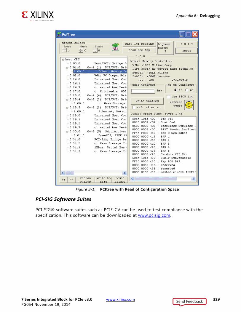
7 Series Integrated Block for PCIe v3.0 www.xilinx.com 329PG054 November 19, 2014
Appendix B: Debugging
PCI-SIG Software Suites
PCI-SIG® software suites such as PCIE-CV can be used to test compliance with the specif ication. This software can be downloaded at www.pcisig.com.
X-Ref Target - Figure B-1
Figure B-1: PCItree with Read of Configuration Space
Send Feedback

7 Series Integrated Block for PCIe v3.0 www.xilinx.com 330PG054 November 19, 2014
Appendix B: Debugging
Simulation DebugThe simulation debug flow for Questa® SIM is illustrated in Figure B-2.
Note: Endpoints that are shaded gray in Figure B-2 indicate that further explanation is provided in this section.
X-Ref Target - Figure B-2
Figure B-2: Questa SIM Debug Flow Diagram
Send Feedback
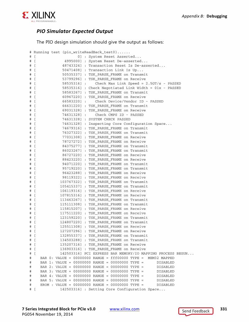
7 Series Integrated Block for PCIe v3.0 www.xilinx.com 331PG054 November 19, 2014
Appendix B: Debugging
PIO Simulator Expected Output
The PIO design simulation should give the output as follows:
# Running test {pio_writeReadBack_test0}......# [ 0] : System Reset Asserted...# [ 4995000] : System Reset De-asserted...# [ 48743324] : Transaction Reset Is De-asserted...# [ 50471408] : Transaction Link Is Up...# [ 50535337] : TSK_PARSE_FRAME on Transmit# [ 53799296] : TSK_PARSE_FRAME on Receive# [ 58535316] : Check Max Link Speed = 2.5GT/s - PASSED# [ 58535316] : Check Negotiated Link Width = 01x - PASSED# [ 58583267] : TSK_PARSE_FRAME on Transmit# [ 60967220] : TSK_PARSE_FRAME on Receive# [ 66583220] : Check Device/Vendor ID - PASSED# [ 66631220] : TSK_PARSE_FRAME on Transmit# [ 69031328] : TSK_PARSE_FRAME on Receive# [ 74631328] : Check CMPS ID - PASSED# [ 74631328] : SYSTEM CHECK PASSED# [ 74631328] : Inspecting Core Configuration Space...# [ 74679316] : TSK_PARSE_FRAME on Transmit# [ 76327322] : TSK_PARSE_FRAME on Transmit# [ 77031308] : TSK_PARSE_FRAME on Receive# [ 78727272] : TSK_PARSE_FRAME on Receive# [ 84375277] : TSK_PARSE_FRAME on Transmit# [ 86023267] : TSK_PARSE_FRAME on Transmit# [ 86727220] : TSK_PARSE_FRAME on Receive# [ 88423220] : TSK_PARSE_FRAME on Receive# [ 94071220] : TSK_PARSE_FRAME on Transmit# [ 95719220] : TSK_PARSE_FRAME on Transmit# [ 96423288] : TSK_PARSE_FRAME on Receive# [ 98119322] : TSK_PARSE_FRAME on Receive# [ 103767322] : TSK_PARSE_FRAME on Transmit# [ 105415337] : TSK_PARSE_FRAME on Transmit# [ 106119316] : TSK_PARSE_FRAME on Receive# [ 107815316] : TSK_PARSE_FRAME on Receive# [ 113463267] : TSK_PARSE_FRAME on Transmit# [ 115111308] : TSK_PARSE_FRAME on Transmit# [ 115815207] : TSK_PARSE_FRAME on Receive# [ 117511220] : TSK_PARSE_FRAME on Receive# [ 123159220] : TSK_PARSE_FRAME on Transmit# [ 124807220] : TSK_PARSE_FRAME on Transmit# [ 125511308] : TSK_PARSE_FRAME on Receive# [ 127207296] : TSK_PARSE_FRAME on Receive# [ 132855337] : TSK_PARSE_FRAME on Transmit# [ 134503288] : TSK_PARSE_FRAME on Transmit# [ 135207316] : TSK_PARSE_FRAME on Receive# [ 136903316] : TSK_PARSE_FRAME on Receive# [ 142503316] PCI EXPRESS BAR MEMORY/IO MAPPING PROCESS BEGUN...# BAR 0: VALUE = 00000000 RANGE = fff00000 TYPE = MEM32 MAPPED# BAR 1: VALUE = 00000000 RANGE = 00000000 TYPE = DISABLED# BAR 2: VALUE = 00000000 RANGE = 00000000 TYPE = DISABLED# BAR 3: VALUE = 00000000 RANGE = 00000000 TYPE = DISABLED# BAR 4: VALUE = 00000000 RANGE = 00000000 TYPE = DISABLED# BAR 5: VALUE = 00000000 RANGE = 00000000 TYPE = DISABLED# EROM : VALUE = 00000000 RANGE = 00000000 TYPE = DISABLED# [ 142503316] : Setting Core Configuration Space...
Send Feedback

7 Series Integrated Block for PCIe v3.0 www.xilinx.com 332PG054 November 19, 2014
Appendix B: Debugging
# [ 142551308] : TSK_PARSE_FRAME on Transmit# [ 144199316] : TSK_PARSE_FRAME on Transmit# [ 144903193] : TSK_PARSE_FRAME on Receive# [ 145847316] : TSK_PARSE_FRAME on Transmit# [ 146567204] : TSK_PARSE_FRAME on Receive# [ 147495316] : TSK_PARSE_FRAME on Transmit# [ 148199270] : TSK_PARSE_FRAME on Receive# [ 149143316] : TSK_PARSE_FRAME on Transmit# [ 149863267] : TSK_PARSE_FRAME on Receive# [ 150791328] : TSK_PARSE_FRAME on Transmit# [ 151495316] : TSK_PARSE_FRAME on Receive# [ 152439322] : TSK_PARSE_FRAME on Transmit# [ 153159316] : TSK_PARSE_FRAME on Receive# [ 154087296] : TSK_PARSE_FRAME on Transmit# [ 154791316] : TSK_PARSE_FRAME on Receive# [ 155735315] : TSK_PARSE_FRAME on Transmit# [ 156455316] : TSK_PARSE_FRAME on Receive# [ 158087322] : TSK_PARSE_FRAME on Receive# [ 171735277] : Transmitting TLPs to Memory 32 Space BAR 0# [ 171783193] : TSK_PARSE_FRAME on Transmit# [ 171991308] : TSK_PARSE_FRAME on Transmit# [ 174247296] : TSK_PARSE_FRAME on Receive# [ 179943316] : Test PASSED --- Write Data: 01020304 successfully received# [ 180103267] : Finished transmission of PCI-Express TLPs# ** Note: $finish : ../tests/sample_tests1.v(317)# Time: 180103267 ps Iteration: 6 Instance: /board/RP/tx_usrapp
Compiling Simulation Libraries
Use the compile_simlib command to compile simulation libraries. This tool is delivered as part of the Xilinx software. For more information, see Vivado Design Suite User Guide: Logic Simulation (UG900) [Ref 15] and Vivado Design Suite Tcl Command Reference Guide (UG835) [Ref 19].
compile_simlib produces a modelsim.ini f ile containing the library mappings. In Questa SIM, type vmap at the prompt to see the current library mappings. The mappings can be updated in the ini f ile, or to map a library at the Questa SIM prompt, type:
vmap [<logical_name>] [<path>]
For example:
Vmap unisims_ver C:\my_unisim_lib
Next StepIf the debug suggestions listed previously do not resolve the issue, open a support case or visit the Xilinx User Community forums to have the appropriate Xilinx expert assist with the issue.
Send Feedback

7 Series Integrated Block for PCIe v3.0 www.xilinx.com 333PG054 November 19, 2014
Appendix B: Debugging
To create a technical support case in WebCase, see the Xilinx website at:
www.xilinx.com/support/clearexpress/websupport.htm
Items to include when opening a case:
° Detailed description of the issue and results of the steps listed above.
° Attach a VCD or WLF dump of the simulation.
To discuss possible solutions, use the Xilinx User Community:
forums.xilinx.com/xlnx/
Hardware DebugHardware issues can range from device recognition issues to problems seen after hours of testing. This section provides debug flow diagrams for some of the most common issues. Endpoints that are shaded gray indicate that more information can be found in sections after Figure B-3.
Send Feedback

7 Series Integrated Block for PCIe v3.0 www.xilinx.com 334PG054 November 19, 2014
Appendix B: Debugging
X-Ref Target - Figure B-3
Figure B-3: Design Fails in Hardware Debug Flow Diagram
Design Fails in Hardware
Does a soft reset fix the problem?(user_lnk_up = 1)
No
Is user_reset deasserted?(user_reset = 0)
No
Is user_lnk_up asserted?(user_lnk_up = 1)
To eliminate FPGA configuration as a root cause, perform a soft restart of the system. Performing asoft reset on the system will keeppower applied and forces re-enumeration of the device.
One reason user_reset stays asserted other than the systemreset being asserted is due to a faulty clock. This might keep thePLL from locking which holdsuser_reset asserted.
YesSee “Link is Training Debug” section.
Yes
Yes
See "FPGA Configuration Time Debug" section.
Is it a multi-lane link?
Multi-lane links are susceptible tocrosstalk and noise when all lanesare switching during training.A quick test for this is forcing onelane operation. This can be done by using an interposer or adapterto isolate the upper lanes or use a tape such as Scotch tape andtape off the upper lanes on theconnector. If it is an embedded board, remove the AC capacitors ifpossible to isolate the lanes.
Yes Force x1 Operation
Does user_lnk_up = 1 when usingas x1 only?
There are potentially issueswith the board layout causing interference when all lanes are switching. See board debug suggestions.
Yes
No
No
No
Do you have a link analyzer?
Use the link analyzer to monitor the training sequence and to determine the point of failure.Have the analyzer trigger on the first TS1 that it recognizes and then compare the output to the LTSSM state machine sequences outlined in Chapter 4 of the PCI Express Base Specification.
Yes
Use Vivado lab tools to determine the point of failure.
Using probes, an LED, Vivado ILAor some other method, determine ifuser_lnk_up is asserted. Whenuser_lnk_up is High, it indicatesthe core has achieved link upmeaning the LTSSM is in L0 stateand the data link layer is in theDL_Active state.
See "Clock Debug" section.
Send Feedback
7 Series Integrated Block for PCIe v3.0 www.xilinx.com 335PG054 November 19, 2014
Appendix B: Debugging
FPGA Configuration Time DebugDevice initialization and configuration issues can be caused by not having the FPGA configured fast enough to enter link training and be recognized by the system. Section 6.6 of PCI Express Base Specification, rev. 2.1 [Ref 2] states two rules that might be impacted by FPGA Configuration Time:
• A component must enter the LTSSM Detect state within 20 ms of the end of the Fundamental reset.
• A system must guarantee that all components intended to be software visible at boot time are ready to receive Configuration Requests within 100 ms of the end of Conventional Reset at the Root Complex.
These statements basically mean the FPGA must be configured within a certain f inite time, and not meeting these requirements could cause problems with link training and device recognition.
Configuration can be accomplished using an onboard PROM or dynamically using JTAG. When using JTAG to configure the device, configuration typically occurs after the Chipset has enumerated each peripheral. After configuring the FPGA, a soft reset is required to restart enumeration and configuration of the device. A soft reset on a Windows based PC is performed by going to Start > Shut Down and then selecting Restart.
To eliminate FPGA configuration as a root cause, you should perform a soft restart of the system. Performing a soft reset on the system keeps power applied and forces re-enumeration of the device. If the device links up and is recognized after a soft reset is performed, then FPGA configuration is most likely the issue. Most typical systems use ATX power supplies which provide some margin on this 100 ms window as the power supply is normally valid before the 100 ms window starts. For more information on FPGA configuration, see FPGA Configuration in Chapter 3.
Link is Training DebugFigure B-4 shows the flowchart for link trained debug.
Send Feedback
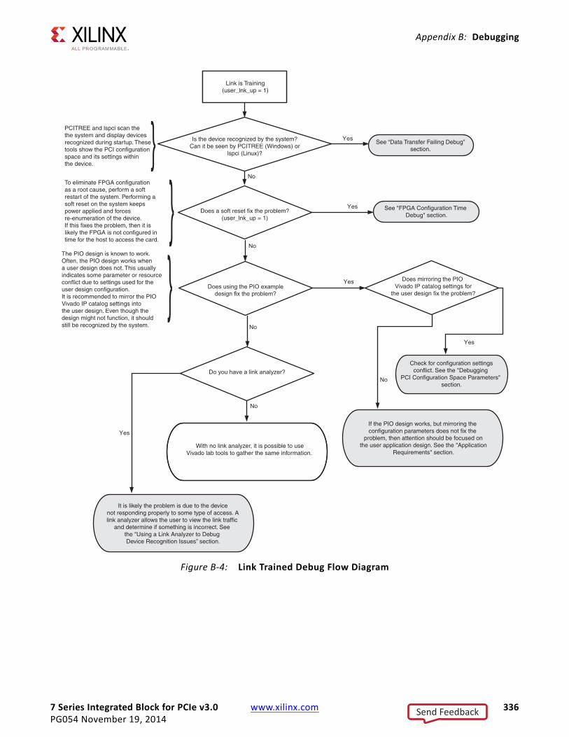
7 Series Integrated Block for PCIe v3.0 www.xilinx.com 336PG054 November 19, 2014
Appendix B: Debugging
X-Ref Target - Figure B-4
Figure B-4: Link Trained Debug Flow Diagram
Link is Training(user_lnk_up = 1)
Is the device recognized by the system?Can it be seen by PCITREE (Windows) or
lspci (Linux)?
Does a soft reset fix the problem?(user_lnk_up = 1)
NoTo eliminate FPGA configuration as a root cause, perform a soft restart of the system. Performing asoft reset on the system keepspower applied and forces re-enumeration of the device.If this fixes the problem, then it is likely the FPGA is not configured intime for the host to access the card.
Yes
Yes
Does using the PIO exampledesign fix the problem?
No
No
NoDo you have a link analyzer?
Does mirroring the PIO Vivado IP catalog settings for
the user design fix the problem?
PCITREE and lspci scan thethe system and display devicesrecognized during startup. Thesetools show the PCI configurationspace and its settings withinthe device.
Yes
The PIO design is known to work.Often, the PIO design works whena user design does not. This usuallyindicates some parameter or resourceconflict due to settings used for theuser design configuration. It is recommended to mirror the PIOVivado IP catalog settings into the user design. Even though thedesign might not function, it should still be recognized by the system.
Yes
Check for configuration settingsconflict. See the "Debugging
PCI Configuration Space Parameters" section.
Yes
If the PIO design works, but mirroring the configuration parameters does not fix the
problem, then attention should be focused onthe user application design. See the "Application
Requirements" section.
No
With no link analyzer, it is possible to useVivado lab tools to gather the same information.
See "FPGA Configuration Time Debug" section.
It is likely the problem is due to the devicenot responding properly to some type of access. Alink analyzer allows the user to view the link traffic
and determine if something is incorrect. See the "Using a Link Analyzer to Debug Device Recognition Issues” section.
See “Data Transfer Failing Debug”section.
Send Feedback

7 Series Integrated Block for PCIe v3.0 www.xilinx.com 337PG054 November 19, 2014
Appendix B: Debugging
FPGA Configuration Time Debug
Device initialization and configuration issues can be caused by not having the FPGA configured fast enough to enter link training and be recognized by the system. Section 6.6 of PCI Express Base Specification, rev. 2.1 [Ref 2] states two rules that might be impacted by FPGA Configuration Time:
• A component must enter the LTSSM Detect state within 20 ms of the end of the Fundamental reset.
• A system must guarantee that all components intended to be software visible at boot time are ready to receive Configuration Requests within 100 ms of the end of Conventional Reset at the Root Complex.
These statements basically mean the FPGA must be configured within a certain f inite time, and not meeting these requirements could cause problems with link training and device recognition.
Configuration can be accomplished using an onboard PROM or dynamically using JTAG. When using JTAG to configure the device, configuration typically occurs after the Chipset has enumerated each peripheral. After configuring the FPGA, a soft reset is required to restart enumeration and configuration of the device. A soft reset on a Windows based PC is performed by going to Start > Shut Down and then selecting Restart.
To eliminate FPGA configuration as a root cause, you should perform a soft restart of the system. Performing a soft reset on the system keeps power applied and forces re-enumeration of the device. If the device links up and is recognized after a soft reset is performed, then FPGA configuration is most likely the issue. Most typical systems use ATX power supplies which provides some margin on this 100 ms window as the power supply is normally valid before the 100 ms window starts. For more information on FPGA configuration, see FPGA Configuration in Chapter 3.
Clock Debug
One reason to not deassert the user_reset_out signal is that the fabric PLL (MMCM) and Transceiver PLL have not locked to the incoming clock. To verify lock, monitor the transceiver CPLLLOCK or QPLLLOCK output and the MMCM LOCK output. If the PLLs do not lock as expected, it is necessary to ensure the incoming reference clock meets the requirements in 7 Series FPGAs GTX/GTH Transceivers User Guide [Ref 12]. The REFCLK signal should be routed to the dedicated reference clock input pins on the serial transceiver, and the user design should instantiate the IBUFDS_GTE2 primitive in the user design. See the 7 Series FPGAs GTX/GTH Transceivers User Guide for more information on PCB layout requirements, including reference clock requirements.
Reference clock jitter can potentially close both the TX and RX eyes, depending on the frequency content of the phase jitter. Therefore, as clean a reference clock as possible must be maintained. Reduce crosstalk on REFCLK by isolating the clock signal from nearby high-speed traces. Maintain a separation of at least 25 mils from the nearest aggressor
Send Feedback
7 Series Integrated Block for PCIe v3.0 www.xilinx.com 338PG054 November 19, 2014
Appendix B: Debugging
signals. The PCI Special Interest Group website provides other tools for ensuring the reference clocks are compliant to the requirements of the PCI Express Specification: www.pcisig.com/specifications/pciexpress/compliance/compliance_library
Debugging PCI Configuration Space Parameters
Often, a user application fails to be recognized by the system, but the Xilinx PIO Example design works. In these cases, the user application is often using a PCI configuration space setting that is interfering with the system systems ability to recognize and allocate resources to the card.
Xilinx solutions for PCI Express handle all configuration transactions internally and generate the correct responses to incoming configuration requests. Chipsets have limits as to the amount of system resources it can allocate and the core must be configured to adhere to these limitations.
The resources requested by the Endpoint are identif ied by the BAR settings within the Endpoint configuration space. You should verify that the resources requested in each BAR can be allocated by the chipset. I/O BARs are especially limited so configuring a large I/O BAR typically prevents the chipset from configuring the device. Generate a core that implements a small amount of memory (approximately 2 KB) to identify if this is the root cause.
The Class Code setting selected in the Vivado IDE can also affect configuration. The Class Code informs the Chipset as to what type of device the Endpoint is. Chipsets might expect a certain type of device to be plugged into the PCI Express slot and configuration might fail if it reads an unexpected Class Code. The BIOS could be configurable to work around this issue.
Use the PIO design with default settings to rule out any device allocation issues. The PIO design default settings have proven to work in all systems encountered when debugging problems. If the default settings allow the device to be recognized, then change the PIO design settings to match the intended user application by changing the PIO configuration in the Vivado IDE. Trial and error might be required to pinpoint the issue if a link analyzer is not available.
Using a link analyzer, it is possible to monitor the link traff ic and possibly determine when during the enumeration and configuration process problems occur.
Send Feedback
7 Series Integrated Block for PCIe v3.0 www.xilinx.com 339PG054 November 19, 2014
Appendix B: Debugging
Application Requirements
During enumeration, it is possible for the chipset to issue TLP traffic that is passed from the core to the backend application. A common oversight when designing custom backend applications is to not have logic which handles every type incoming request. As a result, no response is created and problems arise. The PIO design has the necessary backend functions to respond correctly to any incoming request. It is the responsibility of the application to generate the correct response. These packet types are presented to the application:
• Requests targeting the Expansion ROM (if enabled)
• Message TLPs
• Memory or I/O requests targeting a BAR
• All completion packets
The PIO design, can be used to rule out any of these types of concerns, as the PIO design responds to all incoming transactions to the user application in some way to ensure the host receives the proper response allowing the system to progress. If the PIO design works, but the custom application does not, some transaction is not being handled properly.
The Vivado lab tools should be implemented on the wrapper Receive AXI4-Stream interface to identify if requests targeting the backend application are drained and completed successfully. The AXI4-Stream interface signals that should be probed in the Vivado lab tools are defined in Table B-1, page 342.
Using a Link Analyzer to Debug Device Recognition Issues
In cases where the link is up (user_lnk_up = 1), but the device is not recognized by the system, a link analyzer can help solve the issue. It is likely the FPGA is not responding properly to some type of access. The link view can be used to analyze the traff ic and see if anything looks out of place.
To focus on the issue, it might be necessary to try different triggers. Here are some trigger examples:
• Trigger on the first INIT_FC1 and/or UPDATE_FC in either direction. This allows the analyzer to begin capture after link up.
• The f irst TLP normally transmitted to an Endpoint is the Set Slot Power Limit Message. This usually occurs before Configuration traff ic begins. This might be a good trigger point.
• Trigger on Configuration TLPs.
• Trigger on Memory Read or Memory Write TLPs.
Send Feedback

7 Series Integrated Block for PCIe v3.0 www.xilinx.com 340PG054 November 19, 2014
Appendix B: Debugging
Data Transfer Failing DebugFigure B-5 shows the flowchart for data transfer debug.
X-Ref Target - Figure B-5
Figure B-5: Data Transfer Debug Flow Diagram
Is the system freezing or hanging?
Is use_lnk_up toggling?
No
Yes
Yes
Fatal Error? Blue screen?Other errors?
No
No
No
The most often cause of a systemfreeze or hang is due to acompletion timeout occurring on the host. This happens whenthe host issues a non-postedtransaction (usually a memoryread) to the Endpoint and the Endpoint's user application doesnot properly respond.
If user_lnk_up is toggling, it usuallymeans the physical link is marginal. In these cases, the link can be established but might then fail oncetraffic begins to flow. Use Vivado ILAor probe user_lnk_up to a logicanalyzer and determine if it is toggling.
Link could be marginal and packetsare failing to pass LCRC check.
If read or write transactions do notappear on the AXI interface, it meansthat most likely the incoming packetdid not hit a BAR. Verify incoming
TLP addresses against BARallocation.
A memory write that misses a BAR results in a Non-Fatal error message.
A non-posted transaction that misses aBAR results in a Completion with
UR status.
No
If completion packets fail to reach theirdestination, ensure the packet
contained the correct requester ID ascaptured from the original
Non-Posted TLP.
If other packets fail, ensure the addresstargeted is valid.
Ensure that completions are returnedfor all incoming Non-Posted traffic.
Link is Up (user_lnk_up = 1)Device is recognized by system.
Data Transfers failing.
Do incoming packets appearon the AXI receive interface?
YesErrors flagged by the core are due
to problems on the receive datapath.Use a link analyzer if possible to check incoming packets. See the
"Identifying Errors" section.
Errors are reported to the userinterface on the output cfg_dstatus[3:0].This is a copy of the device statusregister. Use Vivado ILA to monitorthis bus for errors.
Is the problem with receivingor transmitting TLPs?
Do outgoing packets arriveat destination?
Receive Transmit
Send Feedback

7 Series Integrated Block for PCIe v3.0 www.xilinx.com 341PG054 November 19, 2014
Appendix B: Debugging
Identifying ErrorsHardware symptoms of system lock up issues are indicated when the system hangs or a blue screen appears (PC systems). The PCI Express Base Specification, rev. 2.1 [Ref 2] requires that error detection be implemented at the receiver. A system lock up or hang is commonly the result of a Fatal Error and is reported in bit 2 of the receiver Device Status register. Using the Vivado lab tools, monitor the core device status register to see if a fatal error is being reported.
A fatal error reported at the Root complex implies an issue on the transmit side of the EP. The Root Complex Device Status register can often times be seen using PCITree (Windows) or LSPCI (Linux). If a fatal error is detected, see the Transmit section. A Root Complex can often implement Advanced Error Reporting, which further distinguishes the type of error reported. AER provides valuable information as to why a certain error was flagged and is provided as an extended capability within a devices configuration space. Section 7.10 of the PCI Express Base Specification, rev. 2.1 provides more information on AER registers.
Transmit
Fatal Error Detected on Root or Link Partner
Check to make sure the TLP is correctly formed and that the payload (if one is attached) matches what is stated in the header length f ield. The Endpoints device status register does not report errors created by traff ic on the transmit channel.
These signals should be monitored on the Transmit interface to verify all traffic being initiated is correct. See Table 2-10, page 17 for signal descriptions.
• user_lnk_up
• s_axis_tx_tlast
• s_axis_tx_tdata
• s_axis_tx_trb
• s_axis_tx_tvalid
• s_axis_tx_tready
Fatal Error Not Detected
Ensure that the address provided in the TLP header is valid. The kernel mode driver attached to the device is responsible for obtaining the system resources allocated to the device. In a Bus Mastering design, the driver is also responsible for providing the application with a valid address range. System hangs or blue screens might occur if a TLP contains an address that does not target the designated address range for that device.
Send Feedback
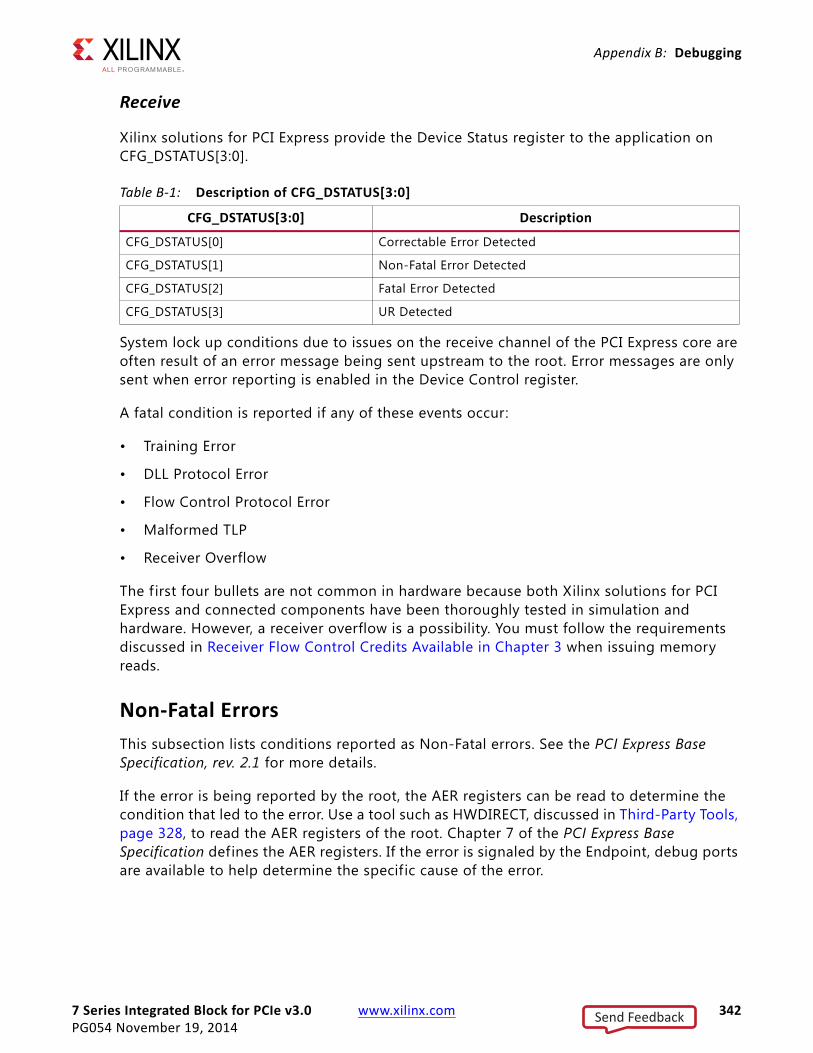
7 Series Integrated Block for PCIe v3.0 www.xilinx.com 342PG054 November 19, 2014
Appendix B: Debugging
Receive
Xilinx solutions for PCI Express provide the Device Status register to the application on CFG_DSTATUS[3:0].
System lock up conditions due to issues on the receive channel of the PCI Express core are often result of an error message being sent upstream to the root. Error messages are only sent when error reporting is enabled in the Device Control register.
A fatal condition is reported if any of these events occur:
• Training Error
• DLL Protocol Error
• Flow Control Protocol Error
• Malformed TLP
• Receiver Overflow
The f irst four bullets are not common in hardware because both Xilinx solutions for PCI Express and connected components have been thoroughly tested in simulation and hardware. However, a receiver overflow is a possibility. You must follow the requirements discussed in Receiver Flow Control Credits Available in Chapter 3 when issuing memory reads.
Non-Fatal ErrorsThis subsection lists conditions reported as Non-Fatal errors. See the PCI Express Base Specification, rev. 2.1 for more details.
If the error is being reported by the root, the AER registers can be read to determine the condition that led to the error. Use a tool such as HWDIRECT, discussed in Third-Party Tools, page 328, to read the AER registers of the root. Chapter 7 of the PCI Express Base Specification defines the AER registers. If the error is signaled by the Endpoint, debug ports are available to help determine the specific cause of the error.
Table B-1: Description of CFG_DSTATUS[3:0]
CFG_DSTATUS[3:0] Description
CFG_DSTATUS[0] Correctable Error Detected
CFG_DSTATUS[1] Non-Fatal Error Detected
CFG_DSTATUS[2] Fatal Error Detected
CFG_DSTATUS[3] UR Detected
Send Feedback
7 Series Integrated Block for PCIe v3.0 www.xilinx.com 343PG054 November 19, 2014
Appendix B: Debugging
Correctable Non-Fatal errors are:
• Receiver Error
• Bad TLP
• Bad DLLP
• Replay Timeout
• Replay NUM Rollover
The f irst three errors listed above are detected by the receiver and are not common in hardware systems. The replay error conditions are signaled by the transmitter. If an ACK is not received for a packet within the allowed time, it is replayed by the transmitter. Throughput can be reduced if many packets are being replayed, and the source can usually be determined by examining the link analyzer or Vivado lab tools captures.
Uncorrectable Non-Fatal errors are:
• Poisoned TLP
• Received ECRC Check Failed
• Unsupported Request (UR)
• Completion Timeout
• Completer Abort
• Unexpected Completion
• ACS Violation
An unsupported request usually indicates that the address in the TLP did not fall within the address space allocated to the BAR. This often points to an issue with the address translation performed by the driver. Ensure also that the BAR has been assigned correctly by the root at start-up. LSPCI or PCItree discussed in Third-Party Tools, page 328 can be used to read the BAR values for each device.
A completion timeout indicates that no completion was returned for a transmitted TLP and is reported by the requester. This can cause the system to hang (could include a blue screen on Windows) and is usually caused when one of the devices locks up and stops responding to incoming TLPs. If the root is reporting the completion timeout, the Vivado lab tools can be used to investigate why the user application did not respond to a TLP (for example, the user application is busy, there are no transmit buffers available, or s_axis_tx_tready is deasserted). If the Endpoint is reporting the Completion timeout, a link analyzer would show the traff ic patterns during the time of failure and would be useful in determining the root cause.
Send Feedback
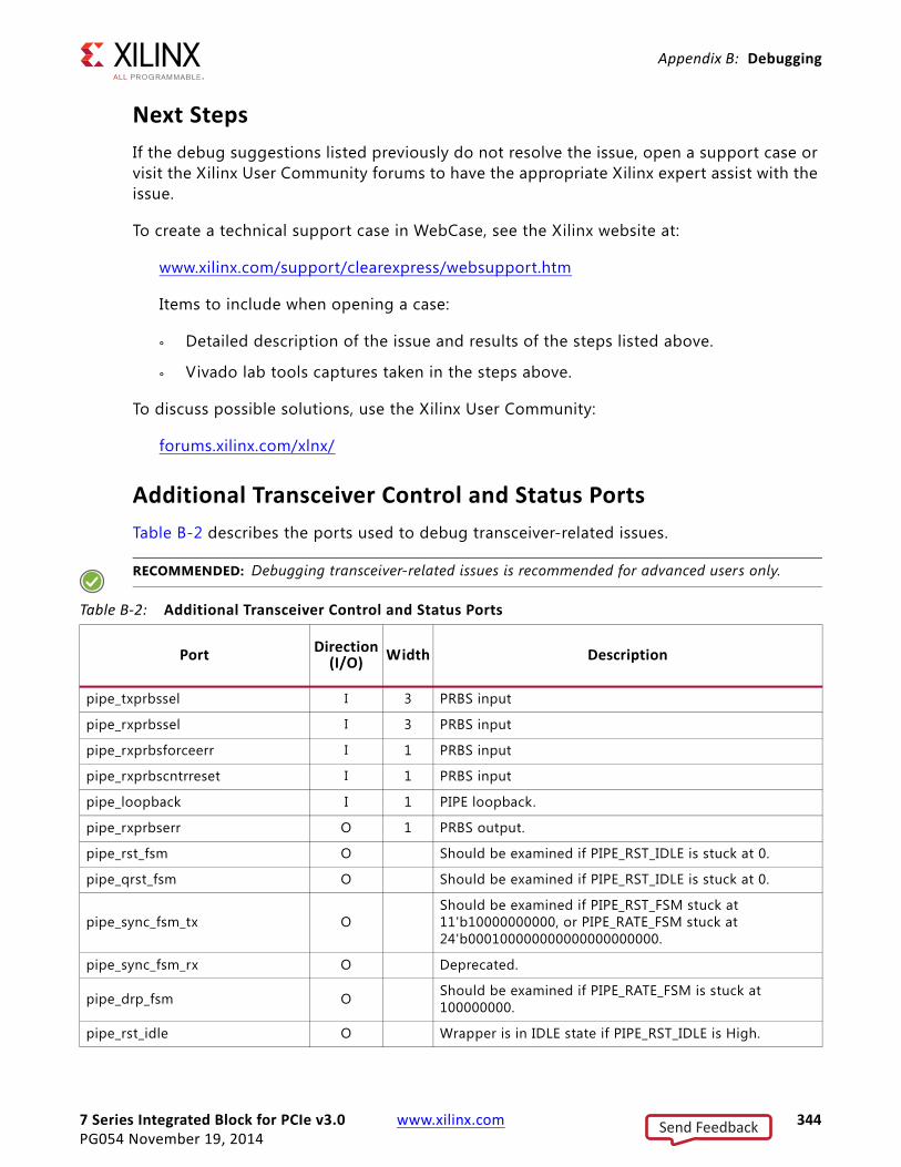
7 Series Integrated Block for PCIe v3.0 www.xilinx.com 344PG054 November 19, 2014
Appendix B: Debugging
Next StepsIf the debug suggestions listed previously do not resolve the issue, open a support case or visit the Xilinx User Community forums to have the appropriate Xilinx expert assist with the issue.
To create a technical support case in WebCase, see the Xilinx website at:
www.xilinx.com/support/clearexpress/websupport.htm
Items to include when opening a case:
° Detailed description of the issue and results of the steps listed above.
° Vivado lab tools captures taken in the steps above.
To discuss possible solutions, use the Xilinx User Community:
forums.xilinx.com/xlnx/
Additional Transceiver Control and Status PortsTable B-2 describes the ports used to debug transceiver-related issues.
RECOMMENDED: Debugging transceiver-related issues is recommended for advanced users only.
Table B-2: Additional Transceiver Control and Status Ports
Port Direction (I/O) Width Description
pipe_txprbssel I 3 PRBS input
pipe_rxprbssel I 3 PRBS input
pipe_rxprbsforceerr I 1 PRBS input
pipe_rxprbscntrreset I 1 PRBS input
pipe_loopback I 1 PIPE loopback.
pipe_rxprbserr O 1 PRBS output.
pipe_rst_fsm O Should be examined if PIPE_RST_IDLE is stuck at 0.
pipe_qrst_fsm O Should be examined if PIPE_RST_IDLE is stuck at 0.
pipe_sync_fsm_tx OShould be examined if PIPE_RST_FSM stuck at 11'b10000000000, or PIPE_RATE_FSM stuck at 24'b000100000000000000000000.
pipe_sync_fsm_rx O Deprecated.
pipe_drp_fsm O Should be examined if PIPE_RATE_FSM is stuck at 100000000.
pipe_rst_idle O Wrapper is in IDLE state if PIPE_RST_IDLE is High.
Send Feedback
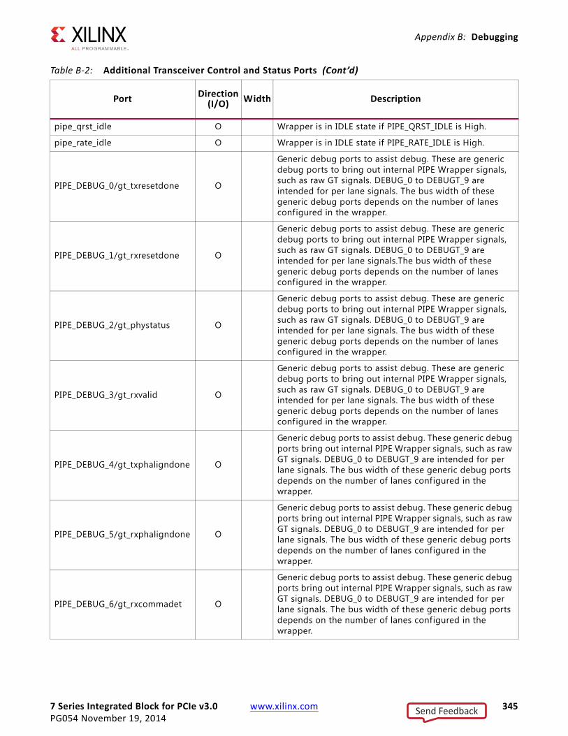
7 Series Integrated Block for PCIe v3.0 www.xilinx.com 345PG054 November 19, 2014
Appendix B: Debugging
pipe_qrst_idle O Wrapper is in IDLE state if PIPE_QRST_IDLE is High.
pipe_rate_idle O Wrapper is in IDLE state if PIPE_RATE_IDLE is High.
PIPE_DEBUG_0/gt_txresetdone O
Generic debug ports to assist debug. These are generic debug ports to bring out internal PIPE Wrapper signals, such as raw GT signals. DEBUG_0 to DEBUGT_9 are intended for per lane signals. The bus width of these generic debug ports depends on the number of lanes configured in the wrapper.
PIPE_DEBUG_1/gt_rxresetdone O
Generic debug ports to assist debug. These are generic debug ports to bring out internal PIPE Wrapper signals, such as raw GT signals. DEBUG_0 to DEBUGT_9 are intended for per lane signals.The bus width of these generic debug ports depends on the number of lanes configured in the wrapper.
PIPE_DEBUG_2/gt_phystatus O
Generic debug ports to assist debug. These are generic debug ports to bring out internal PIPE Wrapper signals, such as raw GT signals. DEBUG_0 to DEBUGT_9 are intended for per lane signals. The bus width of these generic debug ports depends on the number of lanes configured in the wrapper.
PIPE_DEBUG_3/gt_rxvalid O
Generic debug ports to assist debug. These are generic debug ports to bring out internal PIPE Wrapper signals, such as raw GT signals. DEBUG_0 to DEBUGT_9 are intended for per lane signals. The bus width of these generic debug ports depends on the number of lanes configured in the wrapper.
PIPE_DEBUG_4/gt_txphaligndone O
Generic debug ports to assist debug. These generic debug ports bring out internal PIPE Wrapper signals, such as raw GT signals. DEBUG_0 to DEBUGT_9 are intended for per lane signals. The bus width of these generic debug ports depends on the number of lanes configured in the wrapper.
PIPE_DEBUG_5/gt_rxphaligndone O
Generic debug ports to assist debug. These generic debug ports bring out internal PIPE Wrapper signals, such as raw GT signals. DEBUG_0 to DEBUGT_9 are intended for per lane signals. The bus width of these generic debug ports depends on the number of lanes configured in the wrapper.
PIPE_DEBUG_6/gt_rxcommadet O
Generic debug ports to assist debug. These generic debug ports bring out internal PIPE Wrapper signals, such as raw GT signals. DEBUG_0 to DEBUGT_9 are intended for per lane signals. The bus width of these generic debug ports depends on the number of lanes configured in the wrapper.
Table B-2: Additional Transceiver Control and Status Ports (Cont’d)
Port Direction (I/O) Width Description
Send Feedback

7 Series Integrated Block for PCIe v3.0 www.xilinx.com 346PG054 November 19, 2014
Appendix B: Debugging
PIPE_DEBUG_7/gt_rdy O
Generic debug ports to assist debug. These generic debug ports bring out internal PIPE Wrapper signals, such as raw GT signals. DEBUG_0 to DEBUGT_9 are intended for per lane signals. The bus width of these generic debug ports depends on the number of lanes configured in the wrapper.
PIPE_DEBUG_8/user_rx_converge O
Generic debug ports to assist debug. These generic debug ports bring out internal PIPE Wrapper signals, such as raw GT signals. DEBUG_0 to DEBUGT_9 are intended for per lane signals. The bus width of these generic debug ports depends on the number of lanes configured in the wrapper.
PIPE_DEBUG_9/PIPE_TXELECIDLE O
Generic debug ports to assist debug. These generic debug ports bring out internal PIPE Wrapper signals, such as raw GT signals. DEBUG_0 to DEBUGT_9 are intended for per lane signals. The bus width of these generic debug ports depends on the number of lanes configured in the wrapper.
Table B-2: Additional Transceiver Control and Status Ports (Cont’d)
Port Direction (I/O) Width Description
Send Feedback
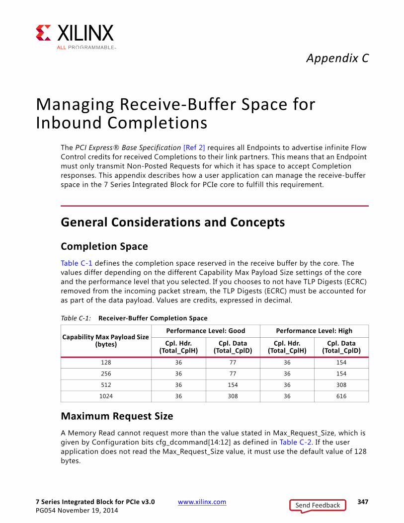
7 Series Integrated Block for PCIe v3.0 www.xilinx.com 347PG054 November 19, 2014
Appendix C
Managing Receive-Buffer Space for Inbound Completions
The PCI Express® Base Specification [Ref 2] requires all Endpoints to advertise infinite Flow Control credits for received Completions to their link partners. This means that an Endpoint must only transmit Non-Posted Requests for which it has space to accept Completion responses. This appendix describes how a user application can manage the receive-buffer space in the 7 Series Integrated Block for PCIe core to fulf ill this requirement.
General Considerations and Concepts
Completion SpaceTable C-1 defines the completion space reserved in the receive buffer by the core. The values differ depending on the different Capability Max Payload Size settings of the core and the performance level that you selected. If you chooses to not have TLP Digests (ECRC) removed from the incoming packet stream, the TLP Digests (ECRC) must be accounted for as part of the data payload. Values are credits, expressed in decimal.
Maximum Request SizeA Memory Read cannot request more than the value stated in Max_Request_Size, which is given by Configuration bits cfg_dcommand[14:12] as defined in Table C-2. If the user application does not read the Max_Request_Size value, it must use the default value of 128 bytes.
Table C-1: Receiver-Buffer Completion Space
Capability Max Payload Size (bytes)
Performance Level: Good Performance Level: High
Cpl. Hdr.(Total_CplH)
Cpl. Data (Total_CplD)
Cpl. Hdr.(Total_CplH)
Cpl. Data(Total_CplD)
128 36 77 36 154
256 36 77 36 154
512 36 154 36 308
1024 36 308 36 616
Send Feedback
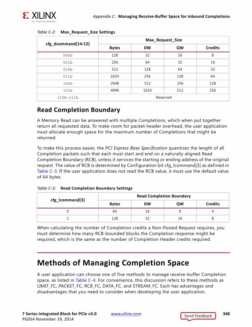
7 Series Integrated Block for PCIe v3.0 www.xilinx.com 348PG054 November 19, 2014
Appendix C: Managing Receive-Buffer Space for Inbound Completions
Read Completion BoundaryA Memory Read can be answered with multiple Completions, which when put together return all requested data. To make room for packet-header overhead, the user application must allocate enough space for the maximum number of Completions that might be returned.
To make this process easier, the PCI Express Base Specification quantizes the length of all Completion packets such that each must start and end on a naturally aligned Read Completion Boundary (RCB), unless it services the starting or ending address of the original request. The value of RCB is determined by Configuration bit cfg_lcommand[3] as defined in Table C-3. If the user application does not read the RCB value, it must use the default value of 64 bytes.
When calculating the number of Completion credits a Non-Posted Request requires, you must determine how many RCB-bounded blocks the Completion response might be required, which is the same as the number of Completion Header credits required.
Methods of Managing Completion SpaceA user application can choose one of f ive methods to manage receive-buffer Completion space, as listed in Table C-4. For convenience, this discussion refers to these methods as LIMIT_FC, PACKET_FC, RCB_FC, DATA_FC, and STREAM_FC. Each has advantages and disadvantages that you need to consider when developing the user application.
Table C-2: Max_Request_Size Settings
cfg_dcommand[14:12]Max_Request_Size
Bytes DW QW Credits
000b 128 32 16 8
001b 256 64 32 16
010b 512 128 64 32
011b 1024 256 128 64
100b 2048 512 256 128
101b 4096 1024 512 256
110b–111b Reserved
Table C-3: Read Completion Boundary Settings
cfg_lcommand[3]Read Completion Boundary
Bytes DW QW Credits
0 64 16 8 4
1 128 32 16 8
Send Feedback

7 Series Integrated Block for PCIe v3.0 www.xilinx.com 349PG054 November 19, 2014
Appendix C: Managing Receive-Buffer Space for Inbound Completions
LIMIT_FC MethodThe LIMIT_FC method is the simplest to implement. The user application assesses the maximum number of outstanding Non-Posted Requests allowed at one time, MAX_NP. To calculate this value, perform these steps:
1. Determine the number of CplH credits required by a Max_Request_Size packet:
Max_Header_Count = ceiling(Max_Request_Size / RCB)
2. Determine the greatest number of maximum-sized Completions supported by the CplD credit pool:
Max_Packet_Count_CplD = floor(CplD / Max_Request_Size)
3. Determine the greatest number of maximum-sized Completions supported by the CplH credit pool:
Max_Packet_Count_CplH = floor(CplH / Max_Header_Count)
4. Use the smaller of the two quantities from steps 2 and 3 to obtain the maximum number of outstanding Non-Posted requests:
MAX_NP = min(Max_Packet_Count_CplH, Max_Packet_Count_CplD)
Table C-4: Managing Receive Completion Space Methods
Method Description Advantage Disadvantage
LIMIT_FC Limit the total number of outstanding NP Requests
Simplest method to implement in user logic
Much Completion capacity goes unused
PACKET_FC
Track the number of outstanding CplH and CplD credits; allocate and deallocate on a per-packet basis
Relatively simple user logic; f iner allocation granularity means less wasted capacity than LIMIT_FC
As with LIMIT_FC, credits for an NP are still tied up until the Request is completely satisf ied
RCB_FC
Track the number of outstanding CplH and CplD credits; allocate and deallocate on a per-RCB basis
Ties up credits for less time than PACKET_FC
More complex user logic than LIMIT_FC or PACKET_FC
DATA_FC
Track the number of outstanding CplH and CplD credits; allocate and deallocate on a per-RCB basis
Lowest amount of wasted capacity
More complex user logic than LIMIT_FC, PACKET_FC, and RCB_FC
STREAM_FC Stream packets out of the core at line rate Very high performance
The user application must accept and process Downstream Completion and Posted Transactions at line rate; Most complex user logic
Send Feedback
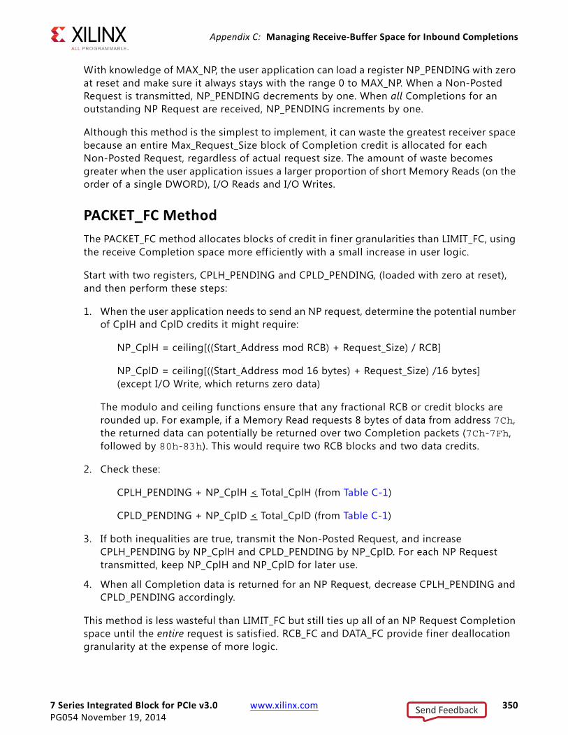
7 Series Integrated Block for PCIe v3.0 www.xilinx.com 350PG054 November 19, 2014
Appendix C: Managing Receive-Buffer Space for Inbound Completions
With knowledge of MAX_NP, the user application can load a register NP_PENDING with zero at reset and make sure it always stays with the range 0 to MAX_NP. When a Non-Posted Request is transmitted, NP_PENDING decrements by one. When all Completions for an outstanding NP Request are received, NP_PENDING increments by one.
Although this method is the simplest to implement, it can waste the greatest receiver space because an entire Max_Request_Size block of Completion credit is allocated for each Non-Posted Request, regardless of actual request size. The amount of waste becomes greater when the user application issues a larger proportion of short Memory Reads (on the order of a single DWORD), I/O Reads and I/O Writes.
PACKET_FC MethodThe PACKET_FC method allocates blocks of credit in f iner granularities than LIMIT_FC, using the receive Completion space more efficiently with a small increase in user logic.
Start with two registers, CPLH_PENDING and CPLD_PENDING, (loaded with zero at reset), and then perform these steps:
1. When the user application needs to send an NP request, determine the potential number of CplH and CplD credits it might require:
NP_CplH = ceiling[((Start_Address mod RCB) + Request_Size) / RCB]
NP_CplD = ceiling[((Start_Address mod 16 bytes) + Request_Size) /16 bytes](except I/O Write, which returns zero data)
The modulo and ceiling functions ensure that any fractional RCB or credit blocks are rounded up. For example, if a Memory Read requests 8 bytes of data from address 7Ch, the returned data can potentially be returned over two Completion packets (7Ch-7Fh, followed by 80h-83h). This would require two RCB blocks and two data credits.
2. Check these:
CPLH_PENDING + NP_CplH < Total_CplH (from Table C-1)
CPLD_PENDING + NP_CplD < Total_CplD (from Table C-1)
3. If both inequalities are true, transmit the Non-Posted Request, and increase CPLH_PENDING by NP_CplH and CPLD_PENDING by NP_CplD. For each NP Request transmitted, keep NP_CplH and NP_CplD for later use.
4. When all Completion data is returned for an NP Request, decrease CPLH_PENDING and CPLD_PENDING accordingly.
This method is less wasteful than LIMIT_FC but still ties up all of an NP Request Completion space until the entire request is satisfied. RCB_FC and DATA_FC provide finer deallocation granularity at the expense of more logic.
Send Feedback
7 Series Integrated Block for PCIe v3.0 www.xilinx.com 351PG054 November 19, 2014
Appendix C: Managing Receive-Buffer Space for Inbound Completions
RCB_FC MethodThe RCB_FC method allocates and de-allocates blocks of credit in RCB granularity. Credit is freed on a per-RCB basis.
As with PACKET_FC, start with two registers, CPLH_PENDING and CPLD_PENDING (loaded with zero at reset).
1. Calculate the number of data credits per RCB:
CplD_PER_RCB = RCB / 16 bytes
2. When the user application needs to send an NP request, determine the potential number of CplH credits it might require. Use this to allocate CplD credits with RCB granularity:
NP_CplH = ceiling[((Start_Address mod RCB) + Request_Size) / RCB]
NP_CplD = NP_CplH × CplD_PER_RCB
3. Check these:
CPLH_PENDING + NP_CplH < Total_CplH
CPLD_PENDING + NP_CplD < Total_CplD
4. If both inequalities are true, transmit the Non-Posted Request, increase CPLH_PENDING by NP_CplH and CPLD_PENDING by NP_CplD.
5. At the start of each incoming Completion, or when that Completion begins at or crosses an RCB without ending at that RCB, decrease CPLH_PENDING by 1 and CPLD_PENDING by CplD_PER_RCB. Any Completion could cross more than one RCB. The number of RCB crossings can be calculated by:
RCB_CROSSED = ceiling[((Lower_Address mod RCB) + Length) / RCB]
Lower_Address and Length are f ields that can be parsed from the Completion header. Alternatively, you can load a register CUR_ADDR with Lower_Address at the start of each incoming Completion, increment per DW or QW as appropriate, then count an RCB whenever CUR_ADDR rolls over.
This method is less wasteful than PACKET_FC but still provides an RCB granularity. If a user application transmits I/O requests, the user application could adopt a policy of only allocating one CplD credit for each I/O Read and zero CplD credits for each I/O Write. The user application would have to match each incoming Completion’s Tag with the Type (Memory Write, I/O Read, I/O Write) of the original NP Request.
Send Feedback
7 Series Integrated Block for PCIe v3.0 www.xilinx.com 352PG054 November 19, 2014
Appendix C: Managing Receive-Buffer Space for Inbound Completions
DATA_FC MethodThe DATA_FC method provides the finest allocation granularity at the expense of logic.
As with PACKET_FC and RCB_FC, start with two registers, CPLH_PENDING and CPLD_PENDING (loaded with zero at reset).
1. When the user application needs to send an NP request, determine the potential number of CplH and CplD credits it might require:
NP_CplH = ceiling[((Start_Address mod RCB) + Request_Size) / RCB]
NP_CplD = ceiling[((Start_Address mod 16 bytes) + Request_Size) / 16 bytes] (except I/O Write, which returns zero data)
2. Check these:
CPLH_PENDING + NP_CplH < Total_CplH
CPLD_PENDING + NP_CplD < Total_CplD
3. If both inequalities are true, transmit the Non-Posted Request, increase CPLH_PENDING by NP_CplH and CPLD_PENDING by NP_CplD.
4. At the start of each incoming Completion, or when that Completion begins at or crosses an RCB without ending at that RCB, decrease CPLH_PENDING by 1. The number of RCB crossings can be calculated by:
RCB_CROSSED = ceiling[((Lower_Address mod RCB) + Length) / RCB]
Lower_Address and Length are f ields that can be parsed from the Completion header. Alternatively, you can load a register CUR_ADDR with Lower_Address at the start of each incoming Completion, increment per DW or QW as appropriate, then count an RCB whenever CUR_ADDR rolls over.
5. At the start of each incoming Completion, or when that Completion begins at or crosses at a naturally aligned credit boundary, decrease CPLD_PENDING by 1. The number of credit-boundary crossings is given by:
DATA_CROSSED = ceiling[((Lower_Address mod 16 B) + Length) / 16 B]
Alternatively, you can load a register CUR_ADDR with Lower_Address at the start of each incoming Completion, increment per DW or QW as appropriate, then count an RCB whenever CUR_ADDR rolls over each 16-byte address boundary.
This method is the least wasteful but requires the greatest amount of user logic. If even f iner granularity is desired, you can scale the Total_CplD value by 2 or 4 to get the number of Completion QWORDs or DWORDs, respectively, and adjust the data calculations accordingly.
Send Feedback
7 Series Integrated Block for PCIe v3.0 www.xilinx.com 353PG054 November 19, 2014
Appendix C: Managing Receive-Buffer Space for Inbound Completions
STREAM_FC MethodWhen configured as an Endpoint, user applications can maximize Downstream (away from Root Complex) data throughput by streaming Memory Read Transactions Upstream (towards the Root Complex) at the highest rate allowed on the Integrated Block Transaction transmit interface. Streaming Memory Reads are allowed only if m_axis_rx_tready can be held asserted; so that Downstream Completion Transactions, along with Posted Transactions, can be presented on the integrated block receive transaction interface and processed at line rate. Asserting m_axis_rx_tready in this manner guarantees that the Completion space within the receive buffer is not oversubscribed (that is, Receiver Overflow does not occur).
Send Feedback
7 Series Integrated Block for PCIe v3.0 www.xilinx.com 354PG054 November 19, 2014
Appendix D
PCIE_2_1 Port DescriptionsThis appendix describes the physical interfaces visible on the 7 Series FPGAs Integrated Block software primitive, PCIE_2_1.
This appendix contains these sections:
• Clock and Reset Interface
• Transaction Layer Interface
• Block RAM Interface
• GTX Transceiver Interface
• Configuration Management Interface
• Dynamic Reconfiguration Port Interface
• TL2 Interface Ports
Clock and Reset InterfaceTable D-1 defines the ports in the Clock and Reset interface.
Table D-1: Clock and Reset Interface Port Descriptions
Port Direction Clock Domain Description
CMRSTN Input USERCLK Configuration Management reset (active-Low). This input resets the PCI™ Configuration Space of the integrated block.
CMSTICKYRSTN Input USERCLK Sticky configuration reset (active-Low). This input resets the sticky registers in the PCI Configuration Space of the integrated block.
DLRSTN Input USERCLK Data Link Layer reset (active-Low). This input resets the Data Link Layer (DLL) of the integrated block.
FUNCLVLRSTN Input USERCLK Not supported. This input must be tied High.
PIPECLK Input PIPECLK PIPE interface clock.
PLRECEIVEDHOTRST Output PIPECLK Received hot reset. When asserted, this output indicates an in-band hot reset has been received.
Send Feedback
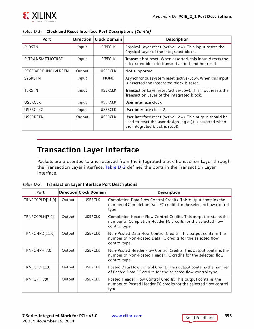
7 Series Integrated Block for PCIe v3.0 www.xilinx.com 355PG054 November 19, 2014
Appendix D: PCIE_2_1 Port Descriptions
Transaction Layer InterfacePackets are presented to and received from the integrated block Transaction Layer through the Transaction Layer interface. Table D-2 defines the ports in the Transaction Layer interface.
PLRSTN Input PIPECLK Physical Layer reset (active-Low). This input resets the Physical Layer of the integrated block.
PLTRANSMITHOTRST Input PIPECLK Transmit hot reset. When asserted, this input directs the integrated block to transmit an in-band hot reset.
RECEIVEDFUNCLVLRSTN Output USERCLK Not supported.
SYSRSTN Input NONE Asynchronous system reset (active-Low). When this input is asserted the integrated block is reset.
TLRSTN Input USERCLK Transaction Layer reset (active-Low). This input resets the Transaction Layer of the integrated block.
USERCLK Input USERCLK User interface clock.
USERCLK2 Input USERCLK User interface clock 2.
USERRSTN Output USERCLK User interface reset (active-Low). This output should be used to reset the user design logic (it is asserted when the integrated block is reset).
Table D-1: Clock and Reset Interface Port Descriptions (Cont’d)
Port Direction Clock Domain Description
Table D-2: Transaction Layer Interface Port Descriptions
Port Direction Clock Domain Description
TRNFCCPLD[11:0] Output USERCLK Completion Data Flow Control Credits. This output contains the number of Completion Data FC credits for the selected flow control type.
TRNFCCPLH[7:0] Output USERCLK Completion Header Flow Control Credits. This output contains the number of Completion Header FC credits for the selected flow control type.
TRNFCNPD[11:0] Output USERCLK Non-Posted Data Flow Control Credits. This output contains the number of Non-Posted Data FC credits for the selected flow control type.
TRNFCNPH[7:0] Output USERCLK Non-Posted Header Flow Control Credits. This output contains the number of Non-Posted Header FC credits for the selected flow control type.
TRNFCPD[11:0] Output USERCLK Posted Data Flow Control Credits. This output contains the number of Posted Data FC credits for the selected flow control type.
TRNFCPH[7:0] Output USERCLK Posted Header Flow Control Credits. This output contains the number of Posted Header FC credits for the selected flow control type.
Send Feedback

7 Series Integrated Block for PCIe v3.0 www.xilinx.com 356PG054 November 19, 2014
Appendix D: PCIE_2_1 Port Descriptions
TRNFCSEL[2:0] Input USERCLK Flow Control Informational Select. This input selects the type of flow control information presented on the TRNFC* signals. Valid values are: • 000b: Receive buffer available space • 001b: Receive credits granted to the link partner • 010b: Receive credits consumed • 100b: Transmit user credits available • 101b: Transmit credit limit • 110b: Transmit credits consumed
TRNLNKUP Output USERCLK Link status output (active-High). When this output is asserted, the Data Link Control and Management State Machine (DLCMSM) is in the DLACTIVE state.
TRNRBARHIT[6:0] Output USERCLK Receive BAR Hit (active-High). This output indicates the BAR(s) targeted by the current receive transaction:• TRNRBARHIT[0]: BAR0 • TRNRBARHIT[1]: BAR1 • TRNRBARHIT[2]: BAR2 • TRNRBARHIT[3]: BAR3 • TRNRBARHIT[4]: BAR4 • TRNRBARHIT[5]: BAR5 • TRNRBARHIT[6]: Expansion ROM Address • TRNRBARHIT[7]: Reserved for future useIf two BARs are configured into a single 64-bit address, both corresponding TRNRBARHITN bits are asserted.
TRNRD[127:0] Output USERCLK Receive Data. This bus contains the packet data being received.
TRNRDSTRDY Input USERCLK Receive Destination Ready (active-High). This input is asserted to indicate that the user application is ready to accept data on TRNRD. Simultaneous assertion of TRNRSRCRDY and TRNRDSTRDY marks the successful transfer of data on TRNRD.
TRNRECRCERR Output USERCLK Receive ECRC Error (active-High). When asserted, this output indicates the current packet in progress has an ECRC error. It is asserted by the integrated block at the packet EOF.
TRNREOF Output USERCLK Receive End-of-Frame (active-High). When asserted, this output indicates the end of a packet.
TRNRERRFWD Output USERCLK Receive Error Forward (active-High). This output marks the current packet in progress as error-poisoned. It is asserted by the integrated block for the entire length of the packet.
TRNRFCPRET Input USERCLK2 Receive Posted Flow Control Credit Return. When asserted for one cycle, this input sets a condition that allows the posted credits to be transmitted to the link partner. The condition is cleared when the posted flow control credits are transmitted.
Table D-2: Transaction Layer Interface Port Descriptions (Cont’d)
Port Direction Clock Domain Description
Send Feedback
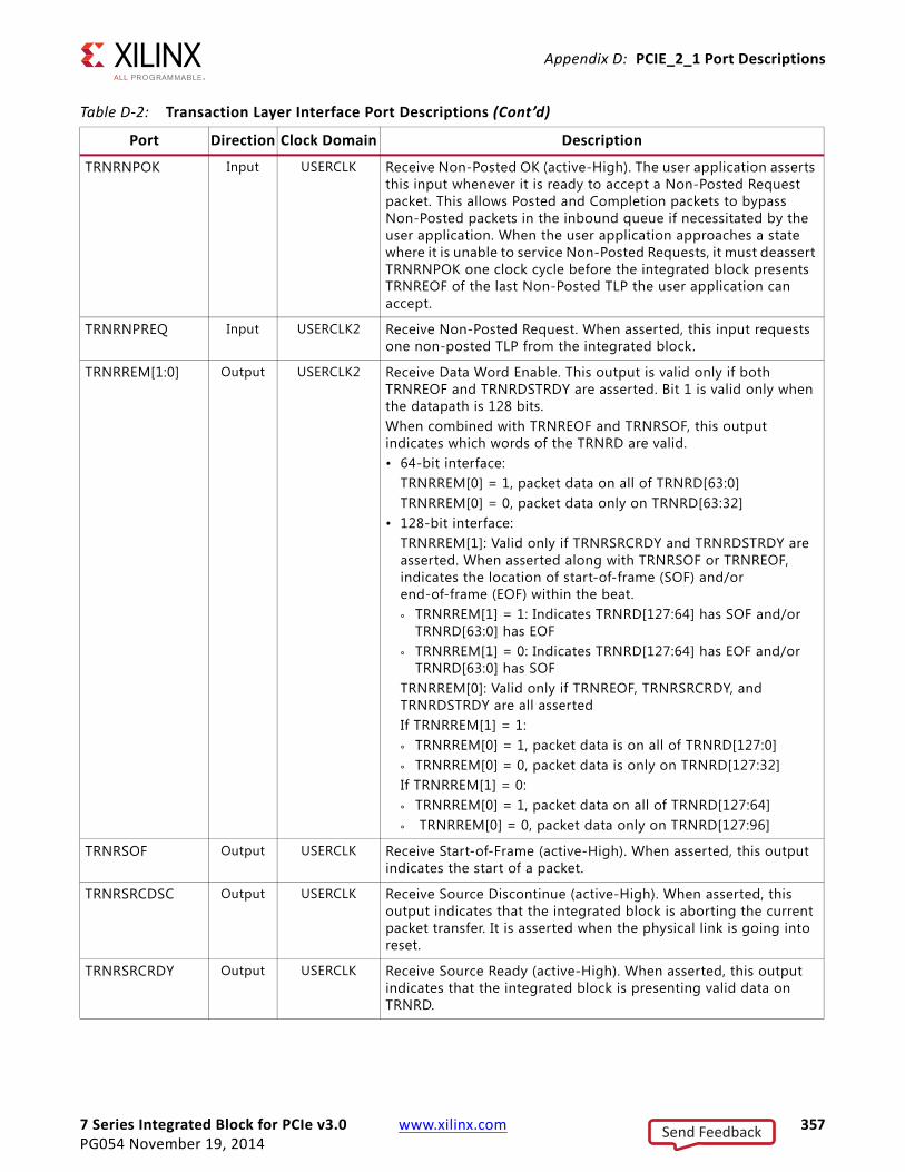
7 Series Integrated Block for PCIe v3.0 www.xilinx.com 357PG054 November 19, 2014
Appendix D: PCIE_2_1 Port Descriptions
TRNRNPOK Input USERCLK Receive Non-Posted OK (active-High). The user application asserts this input whenever it is ready to accept a Non-Posted Request packet. This allows Posted and Completion packets to bypass Non-Posted packets in the inbound queue if necessitated by the user application. When the user application approaches a state where it is unable to service Non-Posted Requests, it must deassert TRNRNPOK one clock cycle before the integrated block presents TRNREOF of the last Non-Posted TLP the user application can accept.
TRNRNPREQ Input USERCLK2 Receive Non-Posted Request. When asserted, this input requests one non-posted TLP from the integrated block.
TRNRREM[1:0] Output USERCLK2 Receive Data Word Enable. This output is valid only if both TRNREOF and TRNRDSTRDY are asserted. Bit 1 is valid only when the datapath is 128 bits.When combined with TRNREOF and TRNRSOF, this output indicates which words of the TRNRD are valid.• 64-bit interface:
TRNRREM[0] = 1, packet data on all of TRNRD[63:0]TRNRREM[0] = 0, packet data only on TRNRD[63:32]
• 128-bit interface:TRNRREM[1]: Valid only if TRNRSRCRDY and TRNRDSTRDY are asserted. When asserted along with TRNRSOF or TRNREOF, indicates the location of start-of-frame (SOF) and/or end-of-frame (EOF) within the beat.
° TRNRREM[1] = 1: Indicates TRNRD[127:64] has SOF and/or TRNRD[63:0] has EOF
° TRNRREM[1] = 0: Indicates TRNRD[127:64] has EOF and/or TRNRD[63:0] has SOF
TRNRREM[0]: Valid only if TRNREOF, TRNRSRCRDY, and TRNRDSTRDY are all assertedIf TRNRREM[1] = 1:
° TRNRREM[0] = 1, packet data is on all of TRNRD[127:0]
° TRNRREM[0] = 0, packet data is only on TRNRD[127:32]If TRNRREM[1] = 0:
° TRNRREM[0] = 1, packet data on all of TRNRD[127:64]
° TRNRREM[0] = 0, packet data only on TRNRD[127:96]
TRNRSOF Output USERCLK Receive Start-of-Frame (active-High). When asserted, this output indicates the start of a packet.
TRNRSRCDSC Output USERCLK Receive Source Discontinue (active-High). When asserted, this output indicates that the integrated block is aborting the current packet transfer. It is asserted when the physical link is going into reset.
TRNRSRCRDY Output USERCLK Receive Source Ready (active-High). When asserted, this output indicates that the integrated block is presenting valid data on TRNRD.
Table D-2: Transaction Layer Interface Port Descriptions (Cont’d)
Port Direction Clock Domain Description
Send Feedback
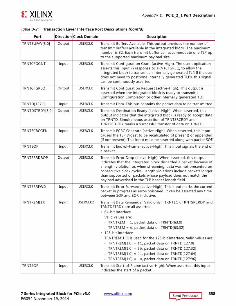
7 Series Integrated Block for PCIe v3.0 www.xilinx.com 358PG054 November 19, 2014
Appendix D: PCIE_2_1 Port Descriptions
TRNTBUFAV[5:0] Output USERCLK Transmit Buffers Available. This output provides the number of transmit buffers available in the integrated block. The maximum number is 32. Each transmit buffer can accommodate one TLP up to the supported maximum payload size.
TRNTCFGGNT Input USERCLK Transmit Configuration Grant (active-High). The user application asserts this input in response to TRNTCFGREQ, to allow the integrated block to transmit an internally generated TLP. If the user does not need to postpone internally generated TLPs, this signal can be continuously asserted.
TRNTCFGREQ Output USERCLK Transmit Configuration Request (active-High). This output is asserted when the integrated block is ready to transmit a Configuration Completion or other internally generated TLP.
TRNTD[127:0] Input USERCLK Transmit Data. This bus contains the packet data to be transmitted.
TRNTDSTRDY[3:0] Output USERCLK Transmit Destination Ready (active-High). When asserted, this output indicates that the integrated block is ready to accept data on TRNTD. Simultaneous assertion of TRNTSRCRDY and TRNTDSTRDY marks a successful transfer of data on TRNTD.
TRNTECRCGEN Input USERCLK Transmit ECRC Generate (active-High). When asserted, this input causes the TLP Digest to be recalculated (if present) or appended (if not present). This input must be asserted along with packet SOF.
TRNTEOF Input USERCLK Transmit End-of-Frame (active-High). This input signals the end of a packet.
TRNTERRDROP Output USERCLK Transmit Error Drop (active-High). When asserted, this output indicates that the integrated block discarded a packet because of a length violation or, when streaming, data was not presented on consecutive clock cycles. Length violations include packets longer than supported or packets whose payload does not match the payload advertised in the TLP header length f ield.
TRNTERRFWD Input USERCLK Transmit Error Forward (active-High). This input marks the current packet in progress as error-poisoned. It can be asserted any time between SOF and EOF, inclusive.
TRNTREM[1:0] Input USERCLK2 Transmit Data Remainder. Valid only if TRNTEOF, TRNTSRCRDY, and TRNTDSTRDY are all asserted.• 64-bit interface
Valid values are:
° TRNTREM = 1, packet data on TRNTD[63:0]
° TRNTREM = 0, packet data on TRNTD[63:32]• 128-bit interface
TRNTREM[1:0] is used for the 128-bit interface. Valid values are:
° TRNTREM[1:0] = 11, packet data on TRNTD[127:0]
° TRNTREM[1:0] = 10, packet data on TRNTD[127:32]
° TRNTREM[1:0] = 01, packet data on TRNTD[127:64]
° TRNTREM[1:0] = 00, packet data on TRNTD[127:96]
TRNTSOF Input USERCLK Transmit Start-of-Frame (active-High). When asserted, this input indicates the start of a packet.
Table D-2: Transaction Layer Interface Port Descriptions (Cont’d)
Port Direction Clock Domain Description
Send Feedback

7 Series Integrated Block for PCIe v3.0 www.xilinx.com 359PG054 November 19, 2014
Appendix D: PCIE_2_1 Port Descriptions
Block RAM InterfaceThe Transmit (TX) and Receive (RX) buffers are implemented with block RAM. Table D-3 defines the TX buffer and RX buffer ports for the Block RAM interface.
TRNTSRCDSC Input USERCLK Transmit Source Discontinue (active-High). When asserted, this input indicates that the user application is aborting the current packet.
TRNTSRCRDY Input USERCLK Transmit Source Ready (active-High). When asserted, this input indicates that the user application is presenting valid data on TRNTD.
TRNTSTR Input USERCLK Transmit Streamed (active-High). When asserted, this input indicates a packet is presented on consecutive clock cycles and transmission on the link can begin before the entire packet has been written to the integrated block.
Table D-2: Transaction Layer Interface Port Descriptions (Cont’d)
Port Direction Clock Domain Description
Table D-3: Block RAM Interface Port Descriptions
Port Direction Clock Domain Description
MIMRXRADDR[12:0] Output USERCLK RX buffer read address
MIMRXRDATA[67:0] Input USERCLK RX buffer read data
MIMRXREN Output USERCLK RX buffer read enable
MIMRXWADDR[12:0] Output USERCLK RX buffer write address
MIMRXWDATA[67:0] Output USERCLK RX buffer write data
MIMRXWEN Output USERCLK RX buffer write enable
MIMTXRADDR[12:0] Output USERCLK TX buffer read address
MIMTXRDATA[68:0] Input USERCLK TX buffer read data
MIMTXREN Output USERCLK TX buffer read enable
MIMTXWADDR[12:0] Output USERCLK TX buffer write address
MIMTXWDATA[68:0] Output USERCLK TX buffer write data
MIMTXWEN Output USERCLK TX buffer write enable
Send Feedback
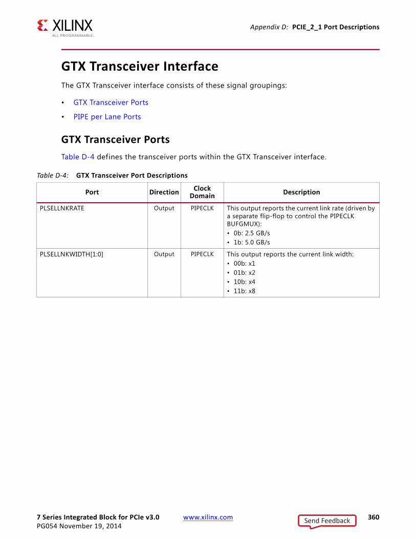
7 Series Integrated Block for PCIe v3.0 www.xilinx.com 360PG054 November 19, 2014
Appendix D: PCIE_2_1 Port Descriptions
GTX Transceiver InterfaceThe GTX Transceiver interface consists of these signal groupings:
• GTX Transceiver Ports
• PIPE per Lane Ports
GTX Transceiver PortsTable D-4 defines the transceiver ports within the GTX Transceiver interface.
Table D-4: GTX Transceiver Port Descriptions
Port Direction Clock Domain Description
PLSELLNKRATE Output PIPECLK This output reports the current link rate (driven by a separate flip-flop to control the PIPECLK BUFGMUX):• 0b: 2.5 GB/s • 1b: 5.0 GB/s
PLSELLNKWIDTH[1:0] Output PIPECLK This output reports the current link width:• 00b: x1• 01b: x2• 10b: x4• 11b: x8
Send Feedback
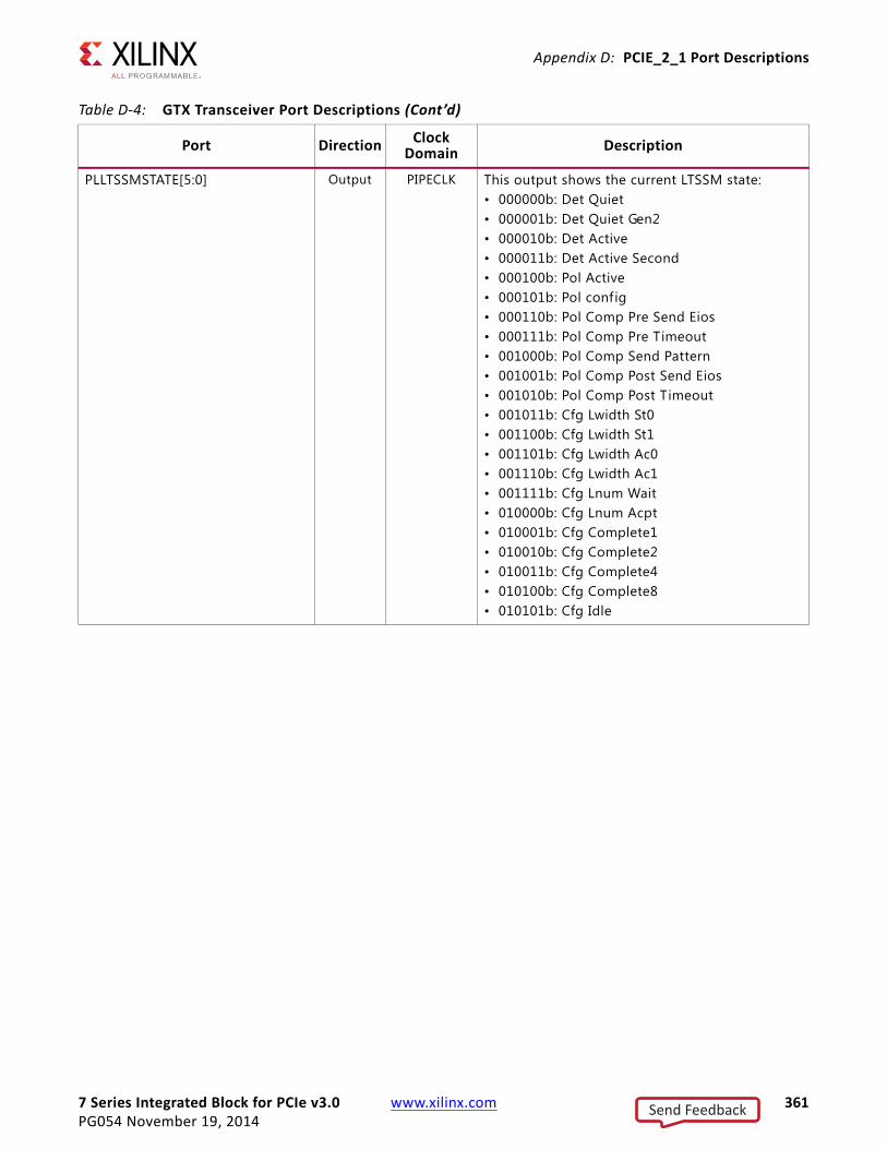
7 Series Integrated Block for PCIe v3.0 www.xilinx.com 361PG054 November 19, 2014
Appendix D: PCIE_2_1 Port Descriptions
PLLTSSMSTATE[5:0] Output PIPECLK This output shows the current LTSSM state:• 000000b: Det Quiet• 000001b: Det Quiet Gen2• 000010b: Det Active• 000011b: Det Active Second• 000100b: Pol Active• 000101b: Pol config• 000110b: Pol Comp Pre Send Eios• 000111b: Pol Comp Pre Timeout• 001000b: Pol Comp Send Pattern• 001001b: Pol Comp Post Send Eios• 001010b: Pol Comp Post Timeout• 001011b: Cfg Lwidth St0• 001100b: Cfg Lwidth St1• 001101b: Cfg Lwidth Ac0• 001110b: Cfg Lwidth Ac1• 001111b: Cfg Lnum Wait• 010000b: Cfg Lnum Acpt• 010001b: Cfg Complete1• 010010b: Cfg Complete2• 010011b: Cfg Complete4• 010100b: Cfg Complete8• 010101b: Cfg Idle
Table D-4: GTX Transceiver Port Descriptions (Cont’d)
Port Direction Clock Domain Description
Send Feedback
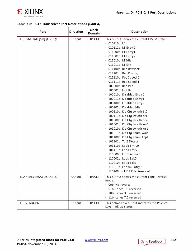
7 Series Integrated Block for PCIe v3.0 www.xilinx.com 362PG054 November 19, 2014
Appendix D: PCIE_2_1 Port Descriptions
PLLTSSMSTATE[5:0] (Cont’d) Output PIPECLK This output shows the current LTSSM state:• 010110b: L0• 010111b: L1 Entry0• 011000b: L1 Entry1• 011001b: L1 Entry2• 011010b: L1 Idle• 011011b: L1 Exit• 011100b: Rec Rcvrlock• 011101b: Rec Rcvrcfg• 011110b: Rec Speed 0• 011111b: Rec Speed 1• 100000b: Rec Idle• 100001b: Hot Rst• 100010b: Disabled Entry0• 100011b: Disabled Entry1• 100100b: Disabled Entry2• 100101b: Disabled Idle• 100110b: Dp Cfg Lwidth St0• 100111b: Dp Cfg Lwidth St1• 101000b: Dp Cfg Lwidth St2• 101001b: Dp Cfg Lwidth Ac0• 101010b: Dp Cfg Lwidth Ac1• 101011b: Dp Cfg Lnum Wait• 101100b: Dp Cfg Lnum Acpt• 101101b: To 2 Detect• 101110b: Lpbk Entry0• 101111b: Lpbk Entry1• 110000b: Lpbk Active0• 110001b: Lpbk Exit0• 110010b: Lpbk Exit1• 110011b: Lpbkm Entry0• 110100b - 111111b: Reserved
PLLANEREVERSALMODE[1:0] Output PIPECLK This output shows the current Lane Reversal mode:• 00b: No reversal• 01b: Lanes 1:0 reversed• 10b: Lanes 3:0 reversed• 11b: Lanes 7:0 reversed
PLPHYLNKUPN Output PIPECLK This active-Low output indicates the Physical Layer link up status.
Table D-4: GTX Transceiver Port Descriptions (Cont’d)
Port Direction Clock Domain Description
Send Feedback
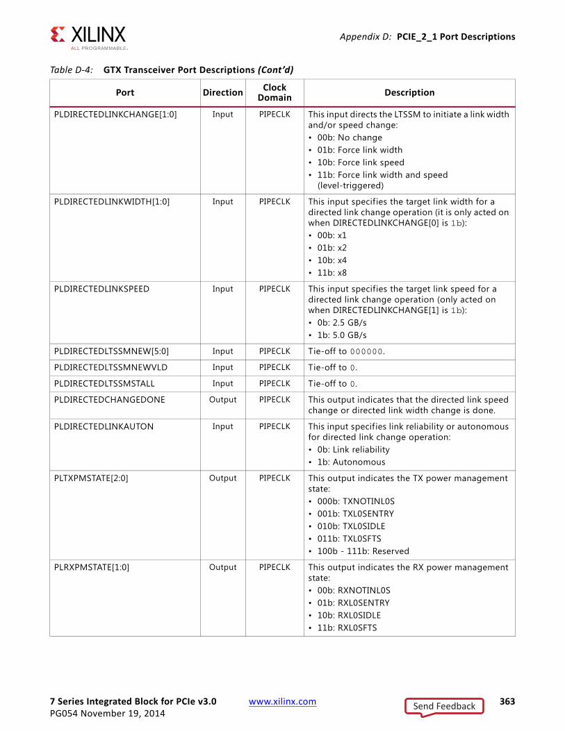
7 Series Integrated Block for PCIe v3.0 www.xilinx.com 363PG054 November 19, 2014
Appendix D: PCIE_2_1 Port Descriptions
PLDIRECTEDLINKCHANGE[1:0] Input PIPECLK This input directs the LTSSM to initiate a link width and/or speed change:• 00b: No change• 01b: Force link width• 10b: Force link speed• 11b: Force link width and speed
(level-triggered)
PLDIRECTEDLINKWIDTH[1:0] Input PIPECLK This input specifies the target link width for a directed link change operation (it is only acted on when DIRECTEDLINKCHANGE[0] is 1b):• 00b: x1• 01b: x2• 10b: x4• 11b: x8
PLDIRECTEDLINKSPEED Input PIPECLK This input specifies the target link speed for a directed link change operation (only acted on when DIRECTEDLINKCHANGE[1] is 1b):• 0b: 2.5 GB/s• 1b: 5.0 GB/s
PLDIRECTEDLTSSMNEW[5:0] Input PIPECLK Tie-off to 000000.
PLDIRECTEDLTSSMNEWVLD Input PIPECLK Tie-off to 0.
PLDIRECTEDLTSSMSTALL Input PIPECLK Tie-off to 0.
PLDIRECTEDCHANGEDONE Output PIPECLK This output indicates that the directed link speed change or directed link width change is done.
PLDIRECTEDLINKAUTON Input PIPECLK This input specifies link reliability or autonomous for directed link change operation:• 0b: Link reliability• 1b: Autonomous
PLTXPMSTATE[2:0] Output PIPECLK This output indicates the TX power management state:• 000b: TXNOTINL0S• 001b: TXL0SENTRY• 010b: TXL0SIDLE• 011b: TXL0SFTS• 100b - 111b: Reserved
PLRXPMSTATE[1:0] Output PIPECLK This output indicates the RX power management state:• 00b: RXNOTINL0S• 01b: RXL0SENTRY• 10b: RXL0SIDLE• 11b: RXL0SFTS
Table D-4: GTX Transceiver Port Descriptions (Cont’d)
Port Direction Clock Domain Description
Send Feedback
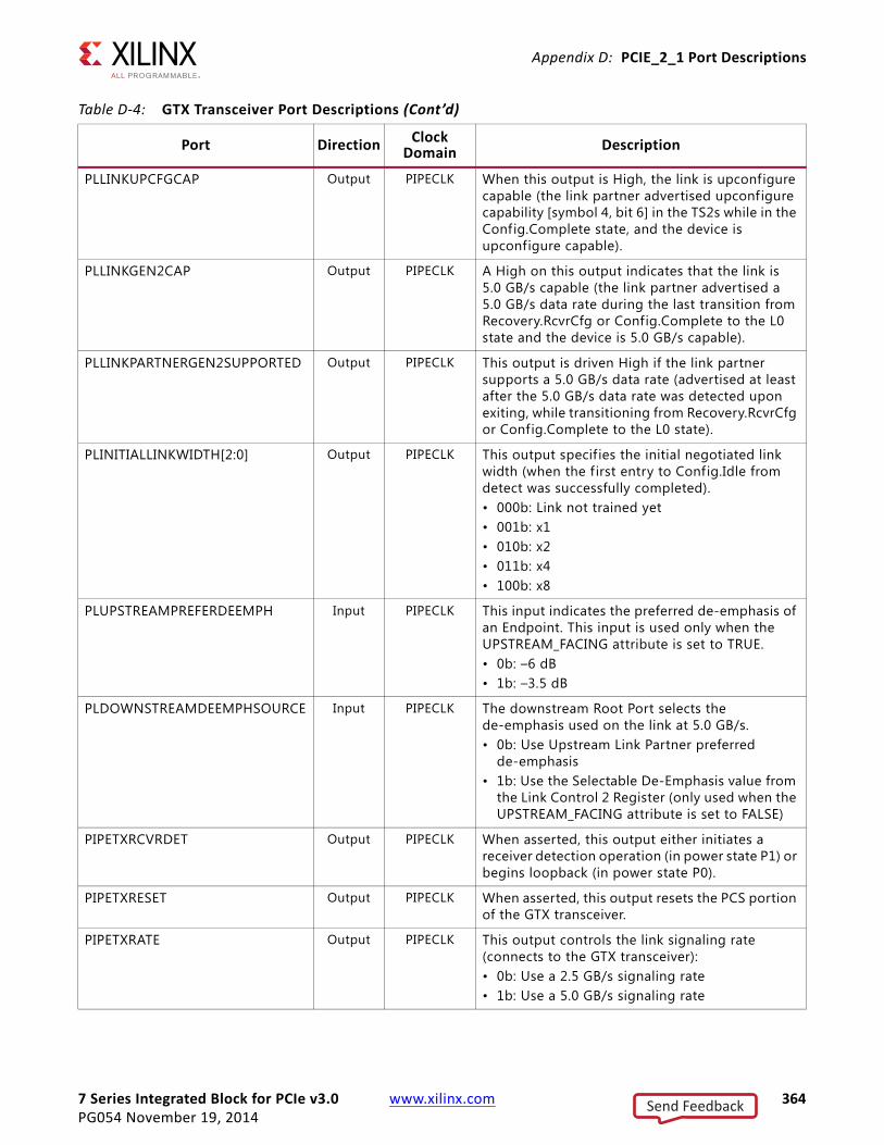
7 Series Integrated Block for PCIe v3.0 www.xilinx.com 364PG054 November 19, 2014
Appendix D: PCIE_2_1 Port Descriptions
PLLINKUPCFGCAP Output PIPECLK When this output is High, the link is upconfigure capable (the link partner advertised upconfigure capability [symbol 4, bit 6] in the TS2s while in the Config.Complete state, and the device is upconfigure capable).
PLLINKGEN2CAP Output PIPECLK A High on this output indicates that the link is 5.0 GB/s capable (the link partner advertised a 5.0 GB/s data rate during the last transition from Recovery.RcvrCfg or Config.Complete to the L0 state and the device is 5.0 GB/s capable).
PLLINKPARTNERGEN2SUPPORTED Output PIPECLK This output is driven High if the link partner supports a 5.0 GB/s data rate (advertised at least after the 5.0 GB/s data rate was detected upon exiting, while transitioning from Recovery.RcvrCfg or Config.Complete to the L0 state).
PLINITIALLINKWIDTH[2:0] Output PIPECLK This output specif ies the initial negotiated link width (when the f irst entry to Config.Idle from detect was successfully completed).• 000b: Link not trained yet • 001b: x1 • 010b: x2 • 011b: x4 • 100b: x8
PLUPSTREAMPREFERDEEMPH Input PIPECLK This input indicates the preferred de-emphasis of an Endpoint. This input is used only when the UPSTREAM_FACING attribute is set to TRUE.• 0b: –6 dB• 1b: –3.5 dB
PLDOWNSTREAMDEEMPHSOURCE Input PIPECLK The downstream Root Port selects the de-emphasis used on the link at 5.0 GB/s. • 0b: Use Upstream Link Partner preferred
de-emphasis• 1b: Use the Selectable De-Emphasis value from
the Link Control 2 Register (only used when the UPSTREAM_FACING attribute is set to FALSE)
PIPETXRCVRDET Output PIPECLK When asserted, this output either initiates a receiver detection operation (in power state P1) or begins loopback (in power state P0).
PIPETXRESET Output PIPECLK When asserted, this output resets the PCS portion of the GTX transceiver.
PIPETXRATE Output PIPECLK This output controls the link signaling rate (connects to the GTX transceiver):• 0b: Use a 2.5 GB/s signaling rate• 1b: Use a 5.0 GB/s signaling rate
Table D-4: GTX Transceiver Port Descriptions (Cont’d)
Port Direction Clock Domain Description
Send Feedback

7 Series Integrated Block for PCIe v3.0 www.xilinx.com 365PG054 November 19, 2014
Appendix D: PCIE_2_1 Port Descriptions
PIPE per Lane PortsTable D-5 defines the PIPE per Lane ports within the GTX Transceiver interface. There are eight copies of the PIPE per lane ports, one for each lane (n = 0 to 7).
PIPETXDEEMPH Output PIPECLK This output selects the transmitter de-emphasis:• 0b: –6 dB de-emphasis• 1b: –3.5 dB de-emphasis
PIPETXMARGIN[2:0] Output PIPECLK This output selects the transmitter voltage levels:• 000b: Normal operating range • 001b: 1200 mV for full swing OR 400 - 700 mV
for half swing• 010b: Required and vendor defined• 011b: Required and vendor defined• 100b: Required and 200 - 400 mV for full swing
OR 100 - 200 mV for half swing if the last value or vendor defined
• 101b: Optional and 200 - 400 mV for full swing OR 100 - 200 mV for half swing if the last value OR vendor defined OR Reserved if no other values supported
• 110b: Optional and 200 - 400 mV for full swing OR 100 - 200 mV for half swing
• 111b: Optional and 200 - 400 mV for full swing OR 100 - 200 mV for half swing if the last value OR Reserved if no other values supported
Table D-4: GTX Transceiver Port Descriptions (Cont’d)
Port Direction Clock Domain Description
Table D-5: PIPE per Lane Port Descriptions
Port Direction Clock Domain Description
PIPERXnCHANISALIGNED Input PIPECLK When this input is asserted, the channel is properly aligned with the master transceiver according to the observed channel bonding sequences in the data stream.
PIPERXnCHARISK[1:0] Input PIPECLK This input determines the control bit(s) for received data:• 0b: Data byte• 1b: Control byteThe lower bit corresponds to the lower byte of PIPERXnDATA[15:0] while the upper bit describes the upper byte.
PIPERXnDATA[15:0] Input PIPECLK This input provides the received data.
PIPERXnELECIDLE Input PIPECLK This asynchronous input indicates electrical idle on the RX.
Send Feedback
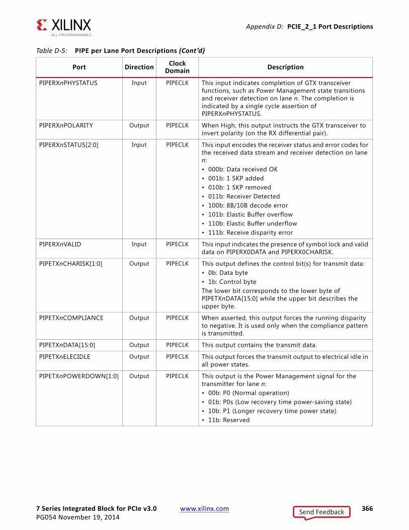
7 Series Integrated Block for PCIe v3.0 www.xilinx.com 366PG054 November 19, 2014
Appendix D: PCIE_2_1 Port Descriptions
PIPERXnPHYSTATUS Input PIPECLK This input indicates completion of GTX transceiver functions, such as Power Management state transitions and receiver detection on lane n. The completion is indicated by a single cycle assertion of PIPERXnPHYSTATUS.
PIPERXnPOLARITY Output PIPECLK When High, this output instructs the GTX transceiver to invert polarity (on the RX differential pair).
PIPERXnSTATUS[2:0] Input PIPECLK This input encodes the receiver status and error codes for the received data stream and receiver detection on lane n:• 000b: Data received OK• 001b: 1 SKP added• 010b: 1 SKP removed• 011b: Receiver Detected• 100b: 8B/10B decode error• 101b: Elastic Buffer overflow• 110b: Elastic Buffer underflow• 111b: Receive disparity error
PIPERXnVALID Input PIPECLK This input indicates the presence of symbol lock and valid data on PIPERX0DATA and PIPERX0CHARISK.
PIPETXnCHARISK[1:0] Output PIPECLK This output defines the control bit(s) for transmit data:• 0b: Data byte• 1b: Control byteThe lower bit corresponds to the lower byte of PIPETXnDATA[15:0] while the upper bit describes the upper byte.
PIPETXnCOMPLIANCE Output PIPECLK When asserted, this output forces the running disparity to negative. It is used only when the compliance pattern is transmitted.
PIPETXnDATA[15:0] Output PIPECLK This output contains the transmit data.
PIPETXnELECIDLE Output PIPECLK This output forces the transmit output to electrical idle in all power states.
PIPETXnPOWERDOWN[1:0] Output PIPECLK This output is the Power Management signal for the transmitter for lane n:• 00b: P0 (Normal operation)• 01b: P0s (Low recovery time power-saving state)• 10b: P1 (Longer recovery time power state)• 11b: Reserved
Table D-5: PIPE per Lane Port Descriptions (Cont’d)
Port Direction Clock Domain Description
Send Feedback

7 Series Integrated Block for PCIe v3.0 www.xilinx.com 367PG054 November 19, 2014
Appendix D: PCIE_2_1 Port Descriptions
Configuration Management InterfaceThe Configuration Management Interface contains these signal groupings:
• Management Interface Ports
• Error Reporting Ports
• Interrupt Generation and Status Ports
• Root Port Specif ic Ports
• Received Message TLP Status Ports
• Power Management Ports
• Received Configuration TLP Status Ports
• Configuration-Specific Register Ports
• Miscellaneous Configuration Management Ports
Management Interface PortsTable D-6 defines the Management Interface ports within the Configuration Management interface. These ports are used when reading and writing the Configuration Space Registers.
Table D-6: Management Interface Port Descriptions
Port Direction Clock Domain Description
CFGMGMTBYTEENN[3:0] Input USERCLK Management Access Byte Enable (active-Low). This 4-bit input provides the byte enables for the configuration register access signal.
CFGMGMTDI[31:0] Input USERCLK Management Data In. This 32-bit data input provides write data to the configuration space inside the integrated block.
CFGMGMTDO[31:0] Output USERCLK Management Data Out. This 32-bit data output obtains read data from the configuration space inside the integrated block.
CFGMGMTDWADDR[9:0] Input USERCLK Management DWORD Address. This 10-bit address input provides a configuration register DWORD address during configuration register accesses.
CFGMGMTRDENN Input USERCLK Management Read Enable (active-Low). This input is the read-enable for configuration register accesses.
CFGMGMTRDWRDONEN Output USERCLK Management Read or Write Done (active-Low). The read-write done signal indicates successful completion of the user configuration register access operation. For a user configuration register read operation, this signal validates the value of the CFGMGMTDO[31:0] data bus.
Send Feedback

7 Series Integrated Block for PCIe v3.0 www.xilinx.com 368PG054 November 19, 2014
Appendix D: PCIE_2_1 Port Descriptions
Error Reporting PortsTable D-7 defines the Error Reporting ports within the Configuration Management interface.
CFGMGMTWRENN Input USERCLK Management Write Enable (active-Low). This input is the write-enable for configuration register accesses.
CFGMGMTWRREADONLYN Input USERCLK Management Write Read-only Bits (active-Low). When asserted, this input indicates the current write should treat a read-only (RO) bit as a read/write (RW) bit, not including bits set by attributes, reserved bits, and bits that reflect status. This permits you to change RO bits (the bit remains RO for link-side accesses).
CFGMGMTWRRW1CASRWN Input USERCLK Management Write RW1C Bit As RW (active-Low). When asserted, this input indicates the current write should treat any RW1C bit as a RW bit. An RW1C bit is cleared by writing a 1 to it and can normally only be set by internal integrated block conditions. The user uses this signal to set the bit to 1.
Table D-6: Management Interface Port Descriptions (Cont’d)
Port Direction Clock Domain Description
Table D-7: Error Reporting Port Descriptions
Port Direction Clock Domain Description
CFGERRACSN Input USERCLK Configuration Error Access Control Services (ACS) Violation (active-Low). The user application assert this signal to report an ACS Violation.
CFGERRAERHEADERLOG[127:0] Input USERCLK Configuration Error AER Header Log. This 128-bit input accepts the header information for the AER Header Log when an error is signaled.Tie-off to 0.
CFGERRAERHEADERLOGSETN Output USERCLK Not used.
CFGERRATOMICEGRESSBLOCKEDN Input USERCLK2 Configuration Error AtomicOp Egress Blocked (active-Low). The user application asserts this signal to report that an Atomic TLP was blocked.
CFGERRCORN Input USERCLK Configuration Error Correctable Error (active-Low). The user application asserts this signal to report a Correctable Error.
CFGERRCPLABORTN Input USERCLK Configuration Error Completion Aborted (active-Low). The user application asserts this signal to report a completion was aborted. This signal is ignored if CFGERRCPLRDYN is deasserted.
Send Feedback
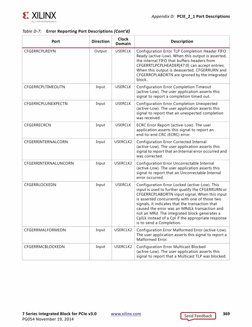
7 Series Integrated Block for PCIe v3.0 www.xilinx.com 369PG054 November 19, 2014
Appendix D: PCIE_2_1 Port Descriptions
CFGERRCPLRDYN Output USERCLK Configuration Error TLP Completion Header FIFO Ready (active-Low). When this output is asserted, the internal FIFO that buffers headers from CFGERRTLPCPLHEADER[47:0] can accept entries. When this output is deasserted, CFGERRURN and CFGERRCPLABORTN are ignored by the integrated block.
CFGERRCPLTIMEOUTN Input USERCLK Configuration Error Completion Timeout (active-Low). The user application asserts this signal to report a completion timed out.
CFGERRCPLUNEXPECTN Input USERCLK Configuration Error Completion Unexpected (active-Low). The user application asserts this signal to report that an unexpected completion was received.
CFGERRECRCN Input USERCLK ECRC Error Report (active-Low). The user application asserts this signal to report an end-to-end CRC (ECRC) error.
CFGERRINTERNALCORN Input USERCLK2 Configuration Error Corrected Internal (active-Low). The user application asserts this signal to report that an Internal error occurred and was corrected.
CFGERRINTERNALUNCORN Input USERCLK2 Configuration Error Uncorrectable Internal (active-Low). The user application asserts this signal to report that an Uncorrectable Internal error occurred.
CFGERRLOCKEDN Input USERCLK Configuration Error Locked (active-Low). This input is used to further qualify the CFGERRURN or CFGERRCPLABORTN input signal. When this input is asserted concurrently with one of those two signals, it indicates that the transaction that caused the error was an MRdLk transaction and not an MRd. The integrated block generates a CplLk instead of a Cpl if the appropriate response is to send a Completion.
CFGERRMALFORMEDN Input USERCLK2 Configuration Error Malformed Error (active-Low). The user application asserts this signal to report a Malformed Error.
CFGERRMCBLOCKEDN Input USERCLK2 Configuration Error Multicast Blocked (active-Low). The user application asserts this signal to report that a Multicast TLP was blocked.
Table D-7: Error Reporting Port Descriptions (Cont’d)
Port Direction Clock Domain Description
Send Feedback
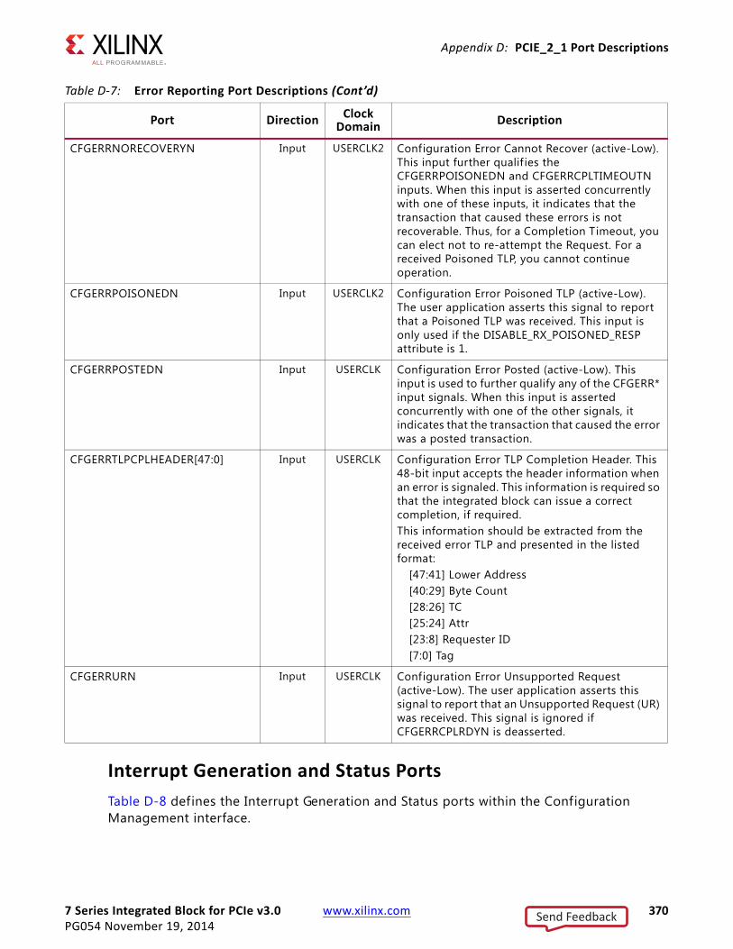
7 Series Integrated Block for PCIe v3.0 www.xilinx.com 370PG054 November 19, 2014
Appendix D: PCIE_2_1 Port Descriptions
Interrupt Generation and Status PortsTable D-8 defines the Interrupt Generation and Status ports within the Configuration Management interface.
CFGERRNORECOVERYN Input USERCLK2 Configuration Error Cannot Recover (active-Low). This input further qualif ies the CFGERRPOISONEDN and CFGERRCPLTIMEOUTN inputs. When this input is asserted concurrently with one of these inputs, it indicates that the transaction that caused these errors is not recoverable. Thus, for a Completion Timeout, you can elect not to re-attempt the Request. For a received Poisoned TLP, you cannot continue operation.
CFGERRPOISONEDN Input USERCLK2 Configuration Error Poisoned TLP (active-Low). The user application asserts this signal to report that a Poisoned TLP was received. This input is only used if the DISABLE_RX_POISONED_RESP attribute is 1.
CFGERRPOSTEDN Input USERCLK Configuration Error Posted (active-Low). This input is used to further qualify any of the CFGERR* input signals. When this input is asserted concurrently with one of the other signals, it indicates that the transaction that caused the error was a posted transaction.
CFGERRTLPCPLHEADER[47:0] Input USERCLK Configuration Error TLP Completion Header. This 48-bit input accepts the header information when an error is signaled. This information is required so that the integrated block can issue a correct completion, if required. This information should be extracted from the received error TLP and presented in the listed format:
[47:41] Lower Address [40:29] Byte Count [28:26] TC [25:24] Attr [23:8] Requester ID [7:0] Tag
CFGERRURN Input USERCLK Configuration Error Unsupported Request (active-Low). The user application asserts this signal to report that an Unsupported Request (UR) was received. This signal is ignored if CFGERRCPLRDYN is deasserted.
Table D-7: Error Reporting Port Descriptions (Cont’d)
Port Direction Clock Domain Description
Send Feedback

7 Series Integrated Block for PCIe v3.0 www.xilinx.com 371PG054 November 19, 2014
Appendix D: PCIE_2_1 Port Descriptions
Table D-8: Interrupt Generation and Status Port Descriptions
Port Direction Clock Domain Description
CFGINTERRUPTASSERTN Input USERCLK Configuration Legacy Interrupt Assert/Deassert Select. This input selects between Assert and Deassert messages for Legacy interrupts when CFGINTERRUPTN is asserted. It is not used for MSI interrupts. Value Message Type: • 0b: Assert • 1b: Deassert
CFGINTERRUPTDI[7:0] Input USERCLK Configuration Interrupt Data In. For Message Signaling Interrupts (MSI), this input provides the portion of the Message Data that the Endpoint must drive to indicate MSI vector number, if Multi-Vector Interrupts are enabled. The value indicated by CFGINTERRUPTMMENABLE[2:0] determines the number of lower-order bits of Message Data that the Endpoint provides; the remaining upper bits of CFGINTERRUPTDI[7:0] are not used. For Single-Vector Interrupts, CFGINTERRUPTDI[7:0] is not used. For Legacy Interrupt Messages (ASSERTINTX, DEASSERTINTX), this input indicates which message type is sent, where Value Legacy Interrupt is:• 00h: INTA • 01h: INTB • 02h: INTC • 03h: INTD
CFGINTERRUPTDO[7:0] Output USERCLK Configuration Interrupt Data Out. This output is the value of the lowest eight bits of the Message Data f ield in the Endpoint MSI capability structure. This value is used in conjunction with CFGINTERRUPTMMENABLE[2:0] to drive CFGINTERRUPTDI[7:0].
CFGINTERRUPTMMENABLE[2:0] Output USERCLK Configuration Interrupt Multiple Message Enabled. This output has the value of the Multiple Message Enable field, where values range from 000b to 101b. A value of 000b indicates that single vector MSI is enabled. Other values indicate the number of bits that can be used for multi-vector MSI.
Send Feedback

7 Series Integrated Block for PCIe v3.0 www.xilinx.com 372PG054 November 19, 2014
Appendix D: PCIE_2_1 Port Descriptions
Root Port Specific PortsTable D-9 defines the Root Port Specif ic ports within the Configuration Management interface.
CFGINTERRUPTMSIENABLE Output USERCLK Configuration Interrupt MSI Enabled. • 0: Only Legacy (INTx) interrupts can be
sent• 1: The Message Signaling Interrupt (MSI)
messaging is enabled
CFGINTERRUPTMSIXENABLE Output USERCLK Configuration Interrupt MSIX Enabled. When asserted, this output indicates that the Message Signaling Interrupt (MSI-X) messaging is enabled.
CFGINTERRUPTMSIXFM Output USERCLK Configuration Interrupt MSIX Function Mask. This output indicates the state of the Function Mask bit in the MSI-X Message Control f ield.
CFGINTERRUPTN Input USERCLK Configuration Interrupt Request (active-Low). When asserted, this input causes the selected interrupt message type to be transmitted by the integrated block. The signal should be asserted until CFGINTERRUPTRDYN is asserted.
CFGINTERRUPTRDYN Output USERCLK Configuration Interrupt Ready (active-Low). This output is the interrupt grant signal. The simultaneous assertion of CFGINTERRUPTRDYN and CFGINTERRUPTN indicates that the integrated block has successfully transmitted the requested interrupt message.
CFGINTERRUPTSTATN Input USERCLK2 Configuration Interrupt Status. If the INTERRUPT_STAT_AUTO attribute is set to 0:• When this input is asserted, the Interrupt
Status bit (bit 3) in the Status register is set.
• When this input is deasserted, the Interrupt Status bit (bit 3) in the Status register is unset.
Table D-8: Interrupt Generation and Status Port Descriptions (Cont’d)
Port Direction Clock Domain Description
Send Feedback
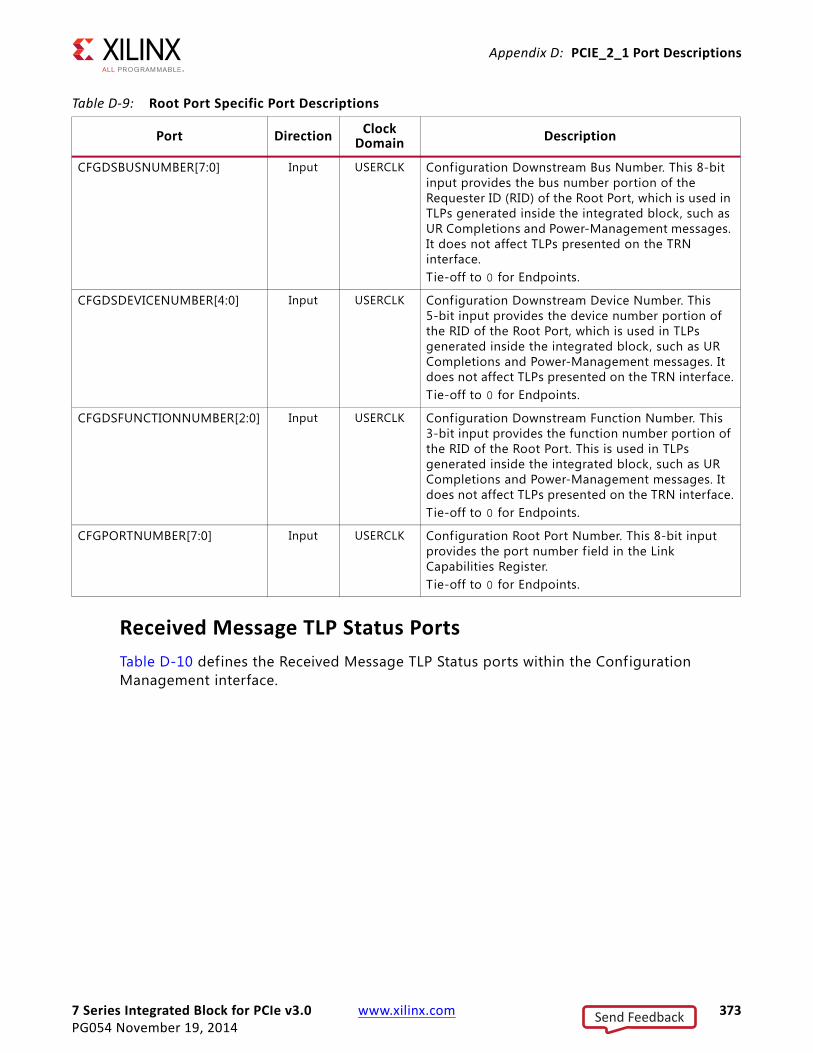
7 Series Integrated Block for PCIe v3.0 www.xilinx.com 373PG054 November 19, 2014
Appendix D: PCIE_2_1 Port Descriptions
Received Message TLP Status PortsTable D-10 defines the Received Message TLP Status ports within the Configuration Management interface.
Table D-9: Root Port Specific Port Descriptions
Port Direction Clock Domain Description
CFGDSBUSNUMBER[7:0] Input USERCLK Configuration Downstream Bus Number. This 8-bit input provides the bus number portion of the Requester ID (RID) of the Root Port, which is used in TLPs generated inside the integrated block, such as UR Completions and Power-Management messages. It does not affect TLPs presented on the TRN interface.Tie-off to 0 for Endpoints.
CFGDSDEVICENUMBER[4:0] Input USERCLK Configuration Downstream Device Number. This 5-bit input provides the device number portion of the RID of the Root Port, which is used in TLPs generated inside the integrated block, such as UR Completions and Power-Management messages. It does not affect TLPs presented on the TRN interface.Tie-off to 0 for Endpoints.
CFGDSFUNCTIONNUMBER[2:0] Input USERCLK Configuration Downstream Function Number. This 3-bit input provides the function number portion of the RID of the Root Port. This is used in TLPs generated inside the integrated block, such as UR Completions and Power-Management messages. It does not affect TLPs presented on the TRN interface.Tie-off to 0 for Endpoints.
CFGPORTNUMBER[7:0] Input USERCLK Configuration Root Port Number. This 8-bit input provides the port number field in the Link Capabilities Register.Tie-off to 0 for Endpoints.
Send Feedback
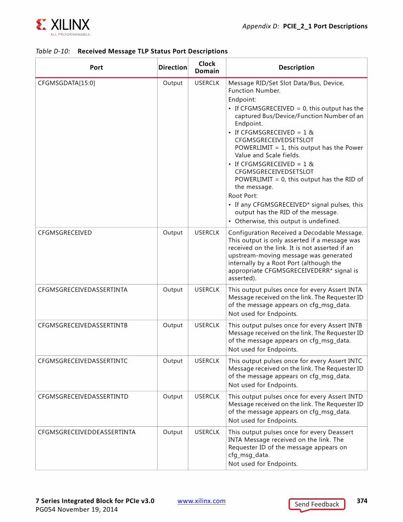
7 Series Integrated Block for PCIe v3.0 www.xilinx.com 374PG054 November 19, 2014
Appendix D: PCIE_2_1 Port Descriptions
Table D-10: Received Message TLP Status Port Descriptions
Port Direction Clock Domain Description
CFGMSGDATA[15:0] Output USERCLK Message RID/Set Slot Data/Bus, Device, Function Number. Endpoint: • If CFGMSGRECEIVED = 0, this output has the
captured Bus/Device/Function Number of an Endpoint.
• If CFGMSGRECEIVED = 1 & CFGMSGRECEIVEDSETSLOTPOWERLIMIT = 1, this output has the Power Value and Scale fields.
• If CFGMSGRECEIVED = 1 & CFGMSGRECEIVEDSETSLOTPOWERLIMIT = 0, this output has the RID of the message.
Root Port: • If any CFGMSGRECEIVED* signal pulses, this
output has the RID of the message. • Otherwise, this output is undefined.
CFGMSGRECEIVED Output USERCLK Configuration Received a Decodable Message. This output is only asserted if a message was received on the link. It is not asserted if an upstream-moving message was generated internally by a Root Port (although the appropriate CFGMSGRECEIVEDERR* signal is asserted).
CFGMSGRECEIVEDASSERTINTA Output USERCLK This output pulses once for every Assert INTA Message received on the link. The Requester ID of the message appears on cfg_msg_data. Not used for Endpoints.
CFGMSGRECEIVEDASSERTINTB Output USERCLK This output pulses once for every Assert INTB Message received on the link. The Requester ID of the message appears on cfg_msg_data. Not used for Endpoints.
CFGMSGRECEIVEDASSERTINTC Output USERCLK This output pulses once for every Assert INTC Message received on the link. The Requester ID of the message appears on cfg_msg_data. Not used for Endpoints.
CFGMSGRECEIVEDASSERTINTD Output USERCLK This output pulses once for every Assert INTD Message received on the link. The Requester ID of the message appears on cfg_msg_data. Not used for Endpoints.
CFGMSGRECEIVEDDEASSERTINTA Output USERCLK This output pulses once for every Deassert INTA Message received on the link. The Requester ID of the message appears on cfg_msg_data. Not used for Endpoints.
Send Feedback
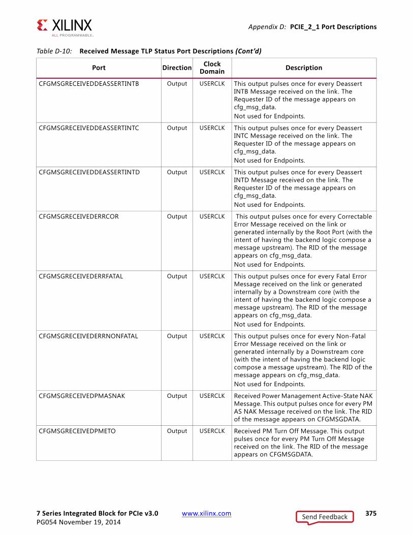
7 Series Integrated Block for PCIe v3.0 www.xilinx.com 375PG054 November 19, 2014
Appendix D: PCIE_2_1 Port Descriptions
CFGMSGRECEIVEDDEASSERTINTB Output USERCLK This output pulses once for every Deassert INTB Message received on the link. The Requester ID of the message appears on cfg_msg_data. Not used for Endpoints.
CFGMSGRECEIVEDDEASSERTINTC Output USERCLK This output pulses once for every Deassert INTC Message received on the link. The Requester ID of the message appears on cfg_msg_data. Not used for Endpoints.
CFGMSGRECEIVEDDEASSERTINTD Output USERCLK This output pulses once for every Deassert INTD Message received on the link. The Requester ID of the message appears on cfg_msg_data. Not used for Endpoints.
CFGMSGRECEIVEDERRCOR Output USERCLK This output pulses once for every Correctable Error Message received on the link or generated internally by the Root Port (with the intent of having the backend logic compose a message upstream). The RID of the message appears on cfg_msg_data. Not used for Endpoints.
CFGMSGRECEIVEDERRFATAL Output USERCLK This output pulses once for every Fatal Error Message received on the link or generated internally by a Downstream core (with the intent of having the backend logic compose a message upstream). The RID of the message appears on cfg_msg_data.Not used for Endpoints.
CFGMSGRECEIVEDERRNONFATAL Output USERCLK This output pulses once for every Non-Fatal Error Message received on the link or generated internally by a Downstream core (with the intent of having the backend logic compose a message upstream). The RID of the message appears on cfg_msg_data.Not used for Endpoints.
CFGMSGRECEIVEDPMASNAK Output USERCLK Received Power Management Active-State NAK Message. This output pulses once for every PM AS NAK Message received on the link. The RID of the message appears on CFGMSGDATA.
CFGMSGRECEIVEDPMETO Output USERCLK Received PM Turn Off Message. This output pulses once for every PM Turn Off Message received on the link. The RID of the message appears on CFGMSGDATA.
Table D-10: Received Message TLP Status Port Descriptions (Cont’d)
Port Direction Clock Domain Description
Send Feedback
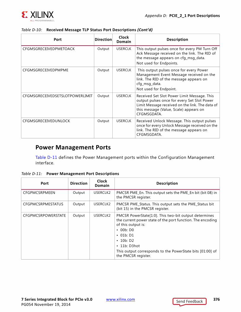
7 Series Integrated Block for PCIe v3.0 www.xilinx.com 376PG054 November 19, 2014
Appendix D: PCIE_2_1 Port Descriptions
Power Management PortsTable D-11 defines the Power Management ports within the Configuration Management interface.
CFGMSGRECEIVEDPMETOACK Output USERCLK This output pulses once for every PM Turn Off Ack Message received on the link. The RID of the message appears on cfg_msg_data.Not used for Endpoints.
CFGMSGRECEIVEDPMPME Output USERCLK This output pulses once for every Power Management Event Message received on the link. The RID of the message appears on cfg_msg_data.Not used for Endpoint.
CFGMSGRECEIVEDSETSLOTPOWERLIMIT Output USERCLK Received Set Slot Power Limit Message. This output pulses once for every Set Slot Power Limit Message received on the link. The data of this message (Value, Scale) appears on CFGMSGDATA.
CFGMSGRECEIVEDUNLOCK Output USERCLK Received Unlock Message. This output pulses once for every Unlock Message received on the link. The RID of the message appears on CFGMSGDATA.
Table D-10: Received Message TLP Status Port Descriptions (Cont’d)
Port Direction Clock Domain Description
Table D-11: Power Management Port Descriptions
Port Direction Clock Domain Description
CFGPMCSRPMEEN Output USERCLK2 PMCSR PME_En. This output sets the PME_En bit (bit 08) in the PMCSR register.
CFGPMCSRPMESTATUS Output USERCLK2 PMCSR PME_Status. This output sets the PME_Status bit (bit 15) in the PMCSR register.
CFGPMCSRPOWERSTATE Output USERCLK2 PMCSR PowerState[1:0]. This two-bit output determines the current power state of the port function. The encoding of this output is:• 00b: D0• 01b: D1• 10b: D2• 11b: D3hotThis output corresponds to the PowerState bits [01:00] of the PMCSR register.
Send Feedback
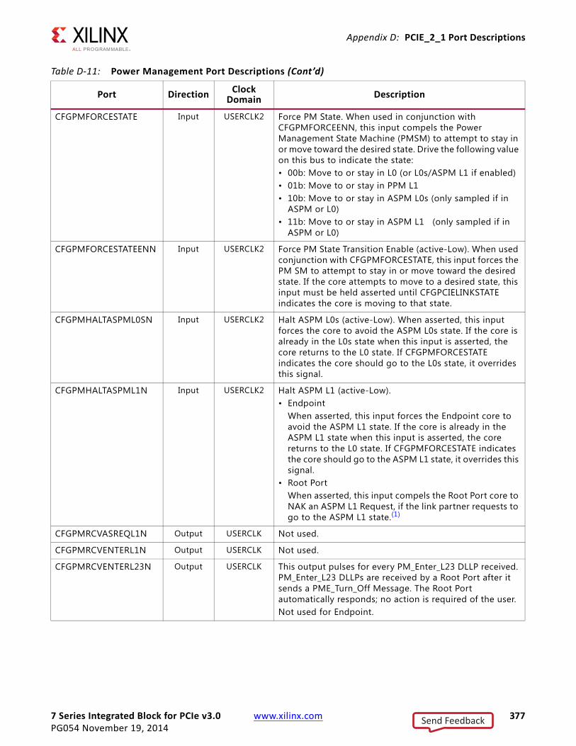
7 Series Integrated Block for PCIe v3.0 www.xilinx.com 377PG054 November 19, 2014
Appendix D: PCIE_2_1 Port Descriptions
CFGPMFORCESTATE Input USERCLK2 Force PM State. When used in conjunction with CFGPMFORCEENN, this input compels the Power Management State Machine (PMSM) to attempt to stay in or move toward the desired state. Drive the following value on this bus to indicate the state:• 00b: Move to or stay in L0 (or L0s/ASPM L1 if enabled)• 01b: Move to or stay in PPM L1• 10b: Move to or stay in ASPM L0s (only sampled if in
ASPM or L0)• 11b: Move to or stay in ASPM L1 (only sampled if in
ASPM or L0)
CFGPMFORCESTATEENN Input USERCLK2 Force PM State Transition Enable (active-Low). When used conjunction with CFGPMFORCESTATE, this input forces the PM SM to attempt to stay in or move toward the desired state. If the core attempts to move to a desired state, this input must be held asserted until CFGPCIELINKSTATE indicates the core is moving to that state.
CFGPMHALTASPML0SN Input USERCLK2 Halt ASPM L0s (active-Low). When asserted, this input forces the core to avoid the ASPM L0s state. If the core is already in the L0s state when this input is asserted, the core returns to the L0 state. If CFGPMFORCESTATE indicates the core should go to the L0s state, it overrides this signal.
CFGPMHALTASPML1N Input USERCLK2 Halt ASPM L1 (active-Low).• Endpoint
When asserted, this input forces the Endpoint core to avoid the ASPM L1 state. If the core is already in the ASPM L1 state when this input is asserted, the core returns to the L0 state. If CFGPMFORCESTATE indicates the core should go to the ASPM L1 state, it overrides this signal.
• Root PortWhen asserted, this input compels the Root Port core to NAK an ASPM L1 Request, if the link partner requests to go to the ASPM L1 state.(1)
CFGPMRCVASREQL1N Output USERCLK Not used.
CFGPMRCVENTERL1N Output USERCLK Not used.
CFGPMRCVENTERL23N Output USERCLK This output pulses for every PM_Enter_L23 DLLP received. PM_Enter_L23 DLLPs are received by a Root Port after it sends a PME_Turn_Off Message. The Root Port automatically responds; no action is required of the user.Not used for Endpoint.
Table D-11: Power Management Port Descriptions (Cont’d)
Port Direction Clock Domain Description
Send Feedback
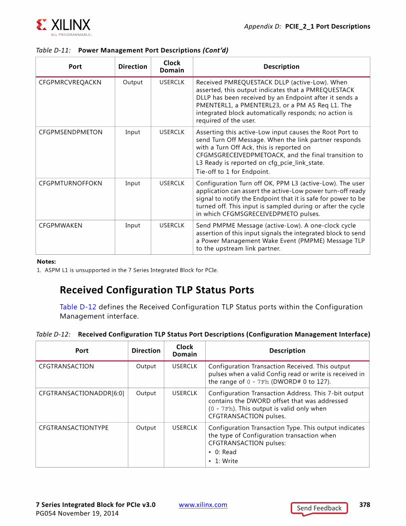
7 Series Integrated Block for PCIe v3.0 www.xilinx.com 378PG054 November 19, 2014
Appendix D: PCIE_2_1 Port Descriptions
Received Configuration TLP Status PortsTable D-12 defines the Received Configuration TLP Status ports within the Configuration Management interface.
CFGPMRCVREQACKN Output USERCLK Received PMREQUESTACK DLLP (active-Low). When asserted, this output indicates that a PMREQUESTACK DLLP has been received by an Endpoint after it sends a PMENTERL1, a PMENTERL23, or a PM AS Req L1. The integrated block automatically responds; no action is required of the user.
CFGPMSENDPMETON Input USERCLK Asserting this active-Low input causes the Root Port to send Turn Off Message. When the link partner responds with a Turn Off Ack, this is reported on CFGMSGRECEIVEDPMETOACK, and the f inal transition to L3 Ready is reported on cfg_pcie_link_state.Tie-off to 1 for Endpoint.
CFGPMTURNOFFOKN Input USERCLK Configuration Turn off OK, PPM L3 (active-Low). The user application can assert the active-Low power turn-off ready signal to notify the Endpoint that it is safe for power to be turned off. This input is sampled during or after the cycle in which CFGMSGRECEIVEDPMETO pulses.
CFGPMWAKEN Input USERCLK Send PMPME Message (active-Low). A one-clock cycle assertion of this input signals the integrated block to send a Power Management Wake Event (PMPME) Message TLP to the upstream link partner.
Notes: 1. ASPM L1 is unsupported in the 7 Series Integrated Block for PCIe.
Table D-11: Power Management Port Descriptions (Cont’d)
Port Direction Clock Domain Description
Table D-12: Received Configuration TLP Status Port Descriptions (Configuration Management Interface)
Port Direction Clock Domain Description
CFGTRANSACTION Output USERCLK Configuration Transaction Received. This output pulses when a valid Config read or write is received in the range of 0 - 7Fh (DWORD# 0 to 127).
CFGTRANSACTIONADDR[6:0] Output USERCLK Configuration Transaction Address. This 7-bit output contains the DWORD offset that was addressed (0 - 7Fh). This output is valid only when CFGTRANSACTION pulses.
CFGTRANSACTIONTYPE Output USERCLK Configuration Transaction Type. This output indicates the type of Configuration transaction when CFGTRANSACTION pulses:• 0: Read• 1: Write
Send Feedback
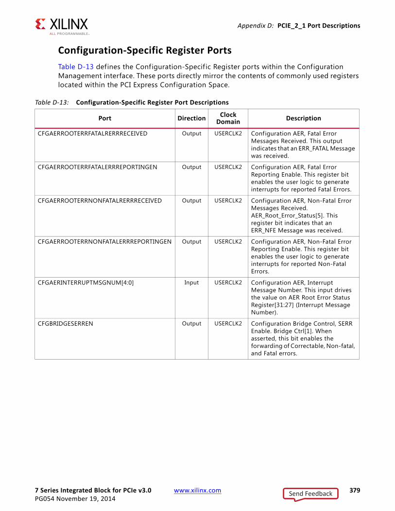
7 Series Integrated Block for PCIe v3.0 www.xilinx.com 379PG054 November 19, 2014
Appendix D: PCIE_2_1 Port Descriptions
Configuration-Specific Register PortsTable D-13 defines the Configuration-Specif ic Register ports within the Configuration Management interface. These ports directly mirror the contents of commonly used registers located within the PCI Express Configuration Space.
Table D-13: Configuration-Specific Register Port Descriptions
Port Direction Clock Domain Description
CFGAERROOTERRFATALRERRRECEIVED Output USERCLK2 Configuration AER, Fatal Error Messages Received. This output indicates that an ERR_FATAL Message was received.
CFGAERROOTERRFATALERRREPORTINGEN Output USERCLK2 Configuration AER, Fatal Error Reporting Enable. This register bit enables the user logic to generate interrupts for reported Fatal Errors.
CFGAERROOTERRNONFATALRERRRECEIVED Output USERCLK2 Configuration AER, Non-Fatal Error Messages Received. AER_Root_Error_Status[5]. This register bit indicates that an ERR_NFE Message was received.
CFGAERROOTERRNONFATALERRREPORTINGEN Output USERCLK2 Configuration AER, Non-Fatal Error Reporting Enable. This register bit enables the user logic to generate interrupts for reported Non-Fatal Errors.
CFGAERINTERRUPTMSGNUM[4:0] Input USERCLK2 Configuration AER, Interrupt Message Number. This input drives the value on AER Root Error Status Register[31:27] (Interrupt Message Number).
CFGBRIDGESERREN Output USERCLK2 Configuration Bridge Control, SERR Enable. Bridge Ctrl[1]. When asserted, this bit enables the forwarding of Correctable, Non-fatal, and Fatal errors.
Send Feedback
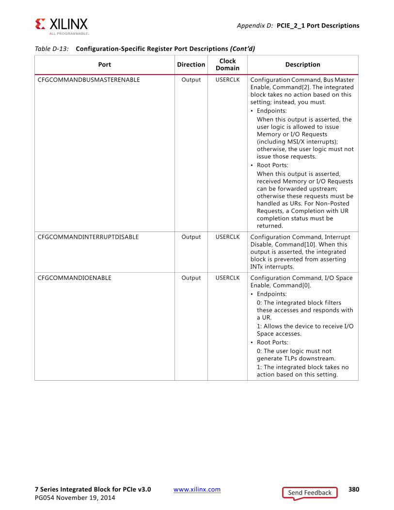
7 Series Integrated Block for PCIe v3.0 www.xilinx.com 380PG054 November 19, 2014
Appendix D: PCIE_2_1 Port Descriptions
CFGCOMMANDBUSMASTERENABLE Output USERCLK Configuration Command, Bus Master Enable, Command[2]. The integrated block takes no action based on this setting; instead, you must. • Endpoints:
When this output is asserted, the user logic is allowed to issue Memory or I/O Requests (including MSI/X interrupts); otherwise, the user logic must not issue those requests.
• Root Ports: When this output is asserted, received Memory or I/O Requests can be forwarded upstream; otherwise these requests must be handled as URs. For Non-Posted Requests, a Completion with UR completion status must be returned.
CFGCOMMANDINTERRUPTDISABLE Output USERCLK Configuration Command, Interrupt Disable, Command[10]. When this output is asserted, the integrated block is prevented from asserting INTx interrupts.
CFGCOMMANDIOENABLE Output USERCLK Configuration Command, I/O Space Enable, Command[0]. • Endpoints:
0: The integrated block f ilters these accesses and responds with a UR.1: Allows the device to receive I/O Space accesses.
• Root Ports: 0: The user logic must not generate TLPs downstream.1: The integrated block takes no action based on this setting.
Table D-13: Configuration-Specific Register Port Descriptions (Cont’d)
Port Direction Clock Domain Description
Send Feedback
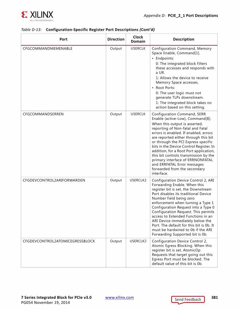
7 Series Integrated Block for PCIe v3.0 www.xilinx.com 381PG054 November 19, 2014
Appendix D: PCIE_2_1 Port Descriptions
CFGCOMMANDMEMENABLE Output USERCLK Configuration Command, Memory Space Enable, Command[1]. • Endpoints:
0: The integrated block f ilters these accesses and responds with a UR. 1: Allows the device to receive Memory Space accesses.
• Root Ports: 0: The user logic must not generate TLPs downstream.1: The integrated block takes no action based on this setting.
CFGCOMMANDSERREN Output USERCLK Configuration Command, SERR Enable (active-Low), Command[8]. When this output is asserted, reporting of Non-fatal and Fatal errors is enabled. If enabled, errors are reported either through this bit or through the PCI Express specif ic bits in the Device Control Register. In addition, for a Root Port application, this bit controls transmission by the primary interface of ERRNONFATAL and ERRFATAL Error messages forwarded from the secondary interface.
CFGDEVCONTROL2ARIFORWARDEN Output USERCLK2 Configuration Device Control 2, ARI Forwarding Enable. When this register bit is set, the Downstream Port disables its traditional Device Number f ield being zero enforcement when turning a Type 1 Configuration Request into a Type 0 Configuration Request. This permits access to Extended Functions in an ARI Device immediately below the Port. The default for this bit is 0b. It must be hardwired to 0b if the ARI Forwarding Supported bit is 0b.
CFGDEVCONTROL2ATOMICEGRESSBLOCK Output USERCLK2 Configuration Device Control 2, Atomic Egress Blocking. When this register bit is set, AtomicOp Requests that target going out this Egress Port must be blocked. The default value of this bit is 0b.
Table D-13: Configuration-Specific Register Port Descriptions (Cont’d)
Port Direction Clock Domain Description
Send Feedback
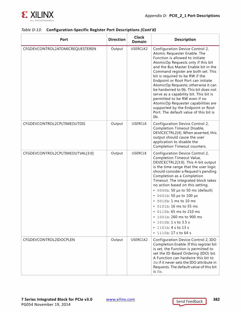
7 Series Integrated Block for PCIe v3.0 www.xilinx.com 382PG054 November 19, 2014
Appendix D: PCIE_2_1 Port Descriptions
CFGDEVCONTROL2ATOMICREQUESTEREN Output USERCLK2 Configuration Device Control 2, Atomic Requester Enable. The Function is allowed to initiate AtomicOp Requests only if this bit and the Bus Master Enable bit in the Command register are both set. This bit is required to be RW if the Endpoint or Root Port can initiate AtomicOp Requests; otherwise it can be hardwired to 0b. This bit does not serve as a capability bit. This bit is permitted to be RW even if no AtomicOp Requester capabilities are supported by the Endpoint or Root Port. The default value of this bit is 0b.
CFGDEVCONTROL2CPLTIMEOUTDIS Output USERCLK Configuration Device Control 2, Completion Timeout Disable, DEVICECTRL2[4]. When asserted, this output should cause the user application to disable the Completion Timeout counters.
CFGDEVCONTROL2CPLTIMEOUTVAL[3:0] Output USERCLK Configuration Device Control 2, Completion Timeout Value, DEVICECTRL2[3:0]. This 4-bit output is the time range that the user logic should consider a Request's pending Completion as a Completion Timeout. The integrated block takes no action based on this setting.• 0000b: 50 µs to 50 ms (default)• 0001b: 50 µs to 100 µs• 0010b: 1 ms to 10 ms• 0101b: 16 ms to 55 ms• 0110b: 65 ms to 210 ms• 1001b: 260 ms to 900 ms• 1010b: 1 s to 3.5 s• 1101b: 4 s to 13 s• 1110b: 17 s to 64 s
CFGDEVCONTROL2IDOCPLEN Output USERCLK2 Configuration Device Control 2, IDO Completion Enable. If this register bit is set, the Function is permitted to set the ID-Based Ordering (IDO) bit. A Function can hardwire this bit to 0b if it never sets the IDO attribute in Requests. The default value of this bit is 0b.
Table D-13: Configuration-Specific Register Port Descriptions (Cont’d)
Port Direction Clock Domain Description
Send Feedback
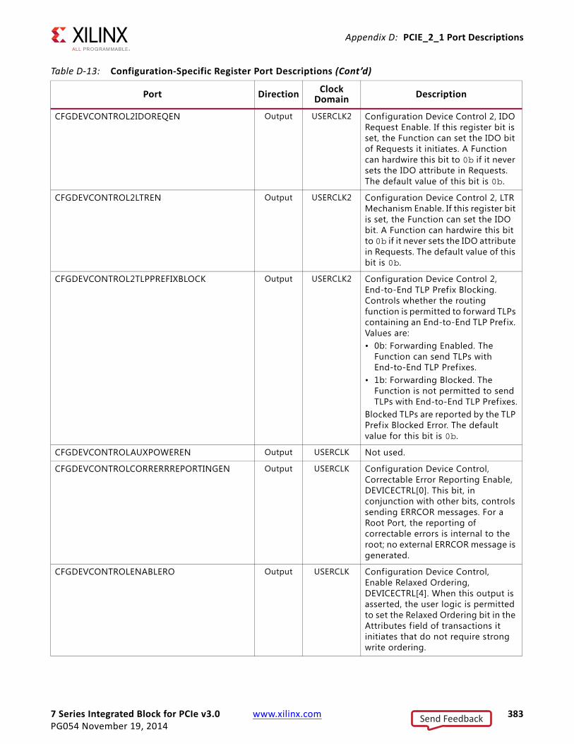
7 Series Integrated Block for PCIe v3.0 www.xilinx.com 383PG054 November 19, 2014
Appendix D: PCIE_2_1 Port Descriptions
CFGDEVCONTROL2IDOREQEN Output USERCLK2 Configuration Device Control 2, IDO Request Enable. If this register bit is set, the Function can set the IDO bit of Requests it initiates. A Function can hardwire this bit to 0b if it never sets the IDO attribute in Requests. The default value of this bit is 0b.
CFGDEVCONTROL2LTREN Output USERCLK2 Configuration Device Control 2, LTR Mechanism Enable. If this register bit is set, the Function can set the IDO bit. A Function can hardwire this bit to 0b if it never sets the IDO attribute in Requests. The default value of this bit is 0b.
CFGDEVCONTROL2TLPPREFIXBLOCK Output USERCLK2 Configuration Device Control 2, End-to-End TLP Prefix Blocking. Controls whether the routing function is permitted to forward TLPs containing an End-to-End TLP Prefix. Values are:• 0b: Forwarding Enabled. The
Function can send TLPs with End-to-End TLP Prefixes.
• 1b: Forwarding Blocked. The Function is not permitted to send TLPs with End-to-End TLP Prefixes.
Blocked TLPs are reported by the TLP Prefix Blocked Error. The default value for this bit is 0b.
CFGDEVCONTROLAUXPOWEREN Output USERCLK Not used.
CFGDEVCONTROLCORRERRREPORTINGEN Output USERCLK Configuration Device Control, Correctable Error Reporting Enable, DEVICECTRL[0]. This bit, in conjunction with other bits, controls sending ERRCOR messages. For a Root Port, the reporting of correctable errors is internal to the root; no external ERRCOR message is generated.
CFGDEVCONTROLENABLERO Output USERCLK Configuration Device Control, Enable Relaxed Ordering, DEVICECTRL[4]. When this output is asserted, the user logic is permitted to set the Relaxed Ordering bit in the Attributes field of transactions it initiates that do not require strong write ordering.
Table D-13: Configuration-Specific Register Port Descriptions (Cont’d)
Port Direction Clock Domain Description
Send Feedback

7 Series Integrated Block for PCIe v3.0 www.xilinx.com 384PG054 November 19, 2014
Appendix D: PCIE_2_1 Port Descriptions
CFGDEVCONTROLEXTTAGEN Output USERCLK Configuration Device Control, Tag Field Enable, DEVICECTRL[8]. When this output is asserted, the user logic can use an 8-bit Tag f ield as a Requester. When this output is deasserted, the user logic is restricted to a 5-bit Tag field. The integrated block does not enforce the number of Tag bits used, either in outgoing request TLPs or incoming Completions.
CFGDEVCONTROLFATALERRREPORTINGEN Output USERCLK Configuration Device Control, Fatal Error Reporting Enable, DEVICECTRL[2]. This bit, in conjunction with other bits, controls sending ERRFATAL messages. For a Root Port, the reporting of correctable errors is internal to the root; no external ERRFATAL message is generated.
CFGDEVCONTROLMAXPAYLOAD[2:0] Output USERCLK Configuration Device Control, MAXPAYLOADSIZE, DEVICECTRL[7:5]. This f ield sets the maximum TLP payload size. As a Receiver, the user logic must handle TLPs as large as the set value. As a Transmitter, the user logic must not generate TLPs exceeding the set value. • 000b: 128-byte maximum payload
size • 001b: 256-byte maximum payload
size • 010b: 512-byte maximum payload
size • 011b: 1024-byte maximum
payload size
Table D-13: Configuration-Specific Register Port Descriptions (Cont’d)
Port Direction Clock Domain Description
Send Feedback

7 Series Integrated Block for PCIe v3.0 www.xilinx.com 385PG054 November 19, 2014
Appendix D: PCIE_2_1 Port Descriptions
CFGDEVCONTROLMAXREADREQ[2:0] Output USERCLK Configuration Device Control, MAXREADREQUESTSIZE, DEVICECTRL[14:12]. This f ield sets the maximum Read Request size for the user logic as a Requester. The user logic must not generate Read Requests with size exceeding the set value. • 000b: 128-byte maximum Read
Request size • 001b: 256-byte maximum Read
Request size • 010b: 512-byte maximum Read
Request size • 011b: 1024-byte maximum Read
Request size • 100b: 2048-byte maximum Read
Request size• 101b: 4096-byte maximum Read
Request size
CFGDEVCONTROLNONFATALREPORTINGEN Output USERCLK Configuration Device Control, Non-Fatal Error Reporting Enable, DEVICECTRL[1]. This bit, in conjunction with other bits, controls sending ERRNONFATAL messages. For a Root Port, the reporting of correctable errors is internal to the root; no external ERRNONFATAL message is generated.
CFGDEVCONTROLNOSNOOPEN Output USERCLK Configuration Device Control, Enable No Snoop, DEVICECTRL[11]. When this output is asserted, the user logic is permitted to set the No Snoop bit in TLPs it initiates that do not require hardware-enforced cache coherency.
CFGDEVCONTROLPHANTOMEN Output USERCLK Configuration Device Control, Phantom Functions Enable, DEVICECTRL[9]. When this output is asserted, the user logic can use unclaimed Functions as Phantom Functions to extend the number of outstanding transaction identif iers. If this output is deasserted, the user logic is not allowed to use Phantom Functions.
Table D-13: Configuration-Specific Register Port Descriptions (Cont’d)
Port Direction Clock Domain Description
Send Feedback

7 Series Integrated Block for PCIe v3.0 www.xilinx.com 386PG054 November 19, 2014
Appendix D: PCIE_2_1 Port Descriptions
CFGDEVCONTROLURERRREPORTINGEN Output USERCLK Configuration Device Control, UR Reporting Enable, DEVICECTRL[3]. This bit, in conjunction with other bits, controls the signaling of URs by sending Error messages.
CFGDEVSTATUSCORRERRDETECTED Output USERCLK Configuration Device Status, Correctable Error Detected, DEVICESTATUS[0]. This output indicates the status of correctable errors detected. Errors are logged in this register regardless of whether error reporting is enabled or not in the Device Control Register.
CFGDEVSTATUSFATALERRDETECTED Output USERCLK Configuration Device Status, Fatal Error Detected, DEVICESTATUS[2]. This output indicates the status of Fatal errors detected. Errors are logged in this register regardless of whether error reporting is enabled or not in the Device Control Register.
CFGDEVSTATUSNONFATALERRDETECTED Output USERCLK Configuration Device Status, Non-Fatal Error Detected, DEVICESTATUS[1]. This output indicates the status of Non-fatal errors detected. Errors are logged in this register regardless of whether error reporting is enabled or not in the Device Control Register.
CFGDEVSTATUSURDETECTED Output USERCLK Configuration Device Status, Unsupported Request Detected, DEVICESTATUS[3]. This output indicates that the integrated block received a UR. Errors are logged in this register regardless of whether error reporting is enabled or not in the Device Control Register.
CFGLINKCONTROLASPMCONTROL[1:0] Output USERCLK Configuration Link Control, ASPM Control, LINKCTRL[1:0]. This 2-bit output indicates the level of ASPM supported, where: • 00b: Disabled• 01b: L0s Entry Enabled• 10b: Not used• 11b: Not used
Table D-13: Configuration-Specific Register Port Descriptions (Cont’d)
Port Direction Clock Domain Description
Send Feedback

7 Series Integrated Block for PCIe v3.0 www.xilinx.com 387PG054 November 19, 2014
Appendix D: PCIE_2_1 Port Descriptions
CFGLINKCONTROLAUTOBANDWIDTHINTEN Output USERCLK Configuration Link Control, Link Autonomous Bandwidth Interrupt Enable, LINKCTRL[11]. When asserted active-Low, this bit enables the generation of an interrupt to indicate that the Link Autonomous Bandwidth Status bit has been set. The core takes no action based on the setting of this bit; user logic must create the interrupt.Not used for Endpoint.
CFGLINKCONTROLBANDWIDTHINTEN Output USERCLK Configuration Link Control, Link Bandwidth Management Interrupt Enable, LINKCTRL[10]. When asserted, active-Low, enables the generation of an interrupt to indicate that the Link Bandwidth Management Status bit has been set. The core takes no action based on the setting of this bit; user logic must create the interrupt.Not used for Endpoint.
CFGLINKCONTROLCLOCKPMEN Output USERCLK Configuration Link Control, Enable Clock Power Management, LINKCTRL[8]. For Endpoints that support a CLKREQ# mechanism:• 0b: Clock power management
disabled• 1b: The device is permitted to use
CLKREQ#The integrated block takes no action based on the setting of this bit; this function must be implemented in external logic.
CFGLINKCONTROLCOMMONCLOCK Output USERCLK Configuration Link Control, Common Clock Configuration, LINKCTRL[6]. When this output is asserted, this component and the component at the opposite end of this Link are operating with a distributed common reference clock. When this output is deasserted, the components are operating with an asynchronous reference clock.
Table D-13: Configuration-Specific Register Port Descriptions (Cont’d)
Port Direction Clock Domain Description
Send Feedback
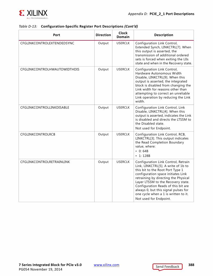
7 Series Integrated Block for PCIe v3.0 www.xilinx.com 388PG054 November 19, 2014
Appendix D: PCIE_2_1 Port Descriptions
CFGLINKCONTROLEXTENDEDSYNC Output USERCLK Configuration Link Control, Extended Synch, LINKCTRL[7]. When this output is asserted, the transmission of additional ordered sets is forced when exiting the L0s state and when in the Recovery state.
CFGLINKCONTROLHWAUTOWIDTHDIS Output USERCLK Configuration Link Control, Hardware Autonomous Width Disable, LINKCTRL[9]. When this output is asserted, the integrated block is disabled from changing the Link width for reasons other than attempting to correct an unreliable Link operation by reducing the Link width.
CFGLINKCONTROLLINKDISABLE Output USERCLK Configuration Link Control, Link Disable, LINKCTRL[4]. When this output is asserted, indicates the Link is disabled and directs the LTSSM to the Disabled state.Not used for Endpoint.
CFGLINKCONTROLRCB Output USERCLK Configuration Link Control, RCB, LINKCTRL[3]. This output indicates the Read Completion Boundary value, where:• 0: 64B• 1: 128B
CFGLINKCONTROLRETRAINLINK Output USERCLK Configuration Link Control, Retrain Link, LINKCTRL[5]. A write of 1b to this bit to the Root Port Type 1 configuration space initiates Link retraining by directing the Physical Layer LTSSM to the Recovery state. Configuration Reads of this bit are always 0, but this signal pulses for one cycle when a 1 is written to it.Not used for Endpoint.
Table D-13: Configuration-Specific Register Port Descriptions (Cont’d)
Port Direction Clock Domain Description
Send Feedback
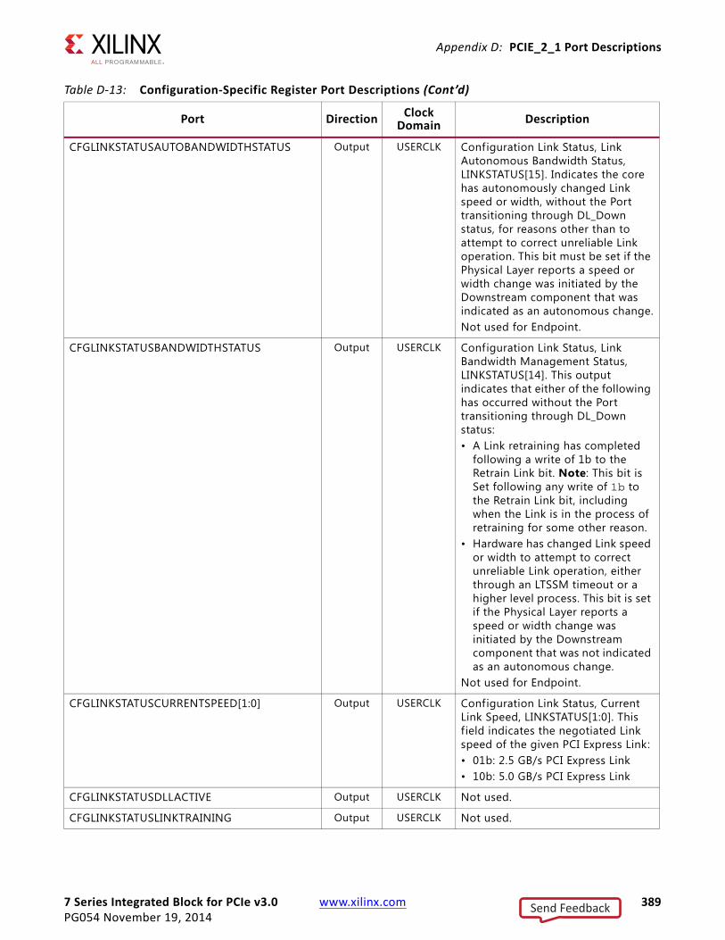
7 Series Integrated Block for PCIe v3.0 www.xilinx.com 389PG054 November 19, 2014
Appendix D: PCIE_2_1 Port Descriptions
CFGLINKSTATUSAUTOBANDWIDTHSTATUS Output USERCLK Configuration Link Status, Link Autonomous Bandwidth Status, LINKSTATUS[15]. Indicates the core has autonomously changed Link speed or width, without the Port transitioning through DL_Down status, for reasons other than to attempt to correct unreliable Link operation. This bit must be set if the Physical Layer reports a speed or width change was initiated by the Downstream component that was indicated as an autonomous change.Not used for Endpoint.
CFGLINKSTATUSBANDWIDTHSTATUS Output USERCLK Configuration Link Status, Link Bandwidth Management Status, LINKSTATUS[14]. This output indicates that either of the following has occurred without the Port transitioning through DL_Down status:• A Link retraining has completed
following a write of 1b to the Retrain Link bit. Note: This bit is Set following any write of 1b to the Retrain Link bit, including when the Link is in the process of retraining for some other reason.
• Hardware has changed Link speed or width to attempt to correct unreliable Link operation, either through an LTSSM timeout or a higher level process. This bit is set if the Physical Layer reports a speed or width change was initiated by the Downstream component that was not indicated as an autonomous change.
Not used for Endpoint.
CFGLINKSTATUSCURRENTSPEED[1:0] Output USERCLK Configuration Link Status, Current Link Speed, LINKSTATUS[1:0]. This f ield indicates the negotiated Link speed of the given PCI Express Link:• 01b: 2.5 GB/s PCI Express Link • 10b: 5.0 GB/s PCI Express Link
CFGLINKSTATUSDLLACTIVE Output USERCLK Not used.
CFGLINKSTATUSLINKTRAINING Output USERCLK Not used.
Table D-13: Configuration-Specific Register Port Descriptions (Cont’d)
Port Direction Clock Domain Description
Send Feedback
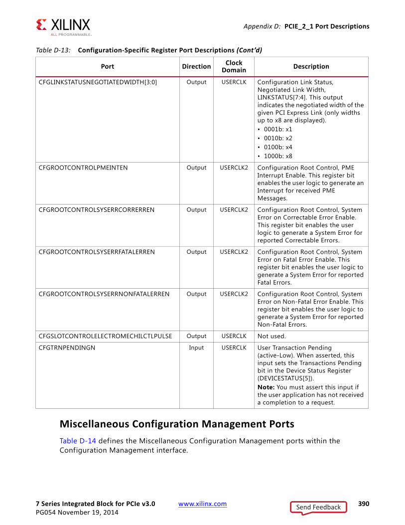
7 Series Integrated Block for PCIe v3.0 www.xilinx.com 390PG054 November 19, 2014
Appendix D: PCIE_2_1 Port Descriptions
Miscellaneous Configuration Management PortsTable D-14 defines the Miscellaneous Configuration Management ports within the Configuration Management interface.
CFGLINKSTATUSNEGOTIATEDWIDTH[3:0] Output USERCLK Configuration Link Status, Negotiated Link Width, LINKSTATUS[7:4]. This output indicates the negotiated width of the given PCI Express Link (only widths up to x8 are displayed). • 0001b: x1 • 0010b: x2 • 0100b: x4 • 1000b: x8
CFGROOTCONTROLPMEINTEN Output USERCLK2 Configuration Root Control, PME Interrupt Enable. This register bit enables the user logic to generate an Interrupt for received PME Messages.
CFGROOTCONTROLSYSERRCORRERREN Output USERCLK2 Configuration Root Control, System Error on Correctable Error Enable. This register bit enables the user logic to generate a System Error for reported Correctable Errors.
CFGROOTCONTROLSYSERRFATALERREN Output USERCLK2 Configuration Root Control, System Error on Fatal Error Enable. This register bit enables the user logic to generate a System Error for reported Fatal Errors.
CFGROOTCONTROLSYSERRNONFATALERREN Output USERCLK2 Configuration Root Control, System Error on Non-Fatal Error Enable. This register bit enables the user logic to generate a System Error for reported Non-Fatal Errors.
CFGSLOTCONTROLELECTROMECHILCTLPULSE Output USERCLK Not used.
CFGTRNPENDINGN Input USERCLK User Transaction Pending (active-Low). When asserted, this input sets the Transactions Pending bit in the Device Status Register (DEVICESTATUS[5]). Note: You must assert this input if the user application has not received a completion to a request.
Table D-13: Configuration-Specific Register Port Descriptions (Cont’d)
Port Direction Clock Domain Description
Send Feedback

7 Series Integrated Block for PCIe v3.0 www.xilinx.com 391PG054 November 19, 2014
Appendix D: PCIE_2_1 Port Descriptions
Table D-14: Miscellaneous Configuration Management Port Descriptions
Port Direction Clock Domain Description
CFGAERECRCCHECKEN Output USERCLK Not used.
CFGAERECRCGENEN Output USERCLK Not used.
CFGDEVID[15:0] Input USERCLK2 Configuration Device ID. This input indicates the value to transfer to the PCI Capability Structure Device ID f ield.
CFGDSN[63:0] Input USERCLK Configuration Device Serial Number. This 64-bit input indicates the value that should be transferred to the Device Serial Number Capability. Bits [31:0] are transferred to the f irst (Lower) DWORD (byte offset 0x4 of the Capability), and bits [63:32] are transferred to the second (Upper) DWORD (byte offset 0x8 of the Capability).
CFGFORCECOMMONCLOCKOFF Input USERCLK2 Force Common Clock Off. When asserted, this input forces the core to behave as if Common Clock was on (but does not set Link Ctrl[7]).
CFGFORCEEXTENDEDSYNCON Input USERCLK2 Force Extended Synch On. When asserted, this input forces the core to behave as if Extended Synch was on (but does not set Link Ctrl[7]).
CFGFORCEMPS[2:0] Input USERCLK2 Force Maximum Payload Size. When ATTR_MPS_FORCE = 1, the core uses this MPS value to check the payload size of received TLPs and for replay/ACKNAK time-outs, instead of using Device Ctrl[7:5]. It does not change Device Ctrl[7:5].
CFGPCIECAPINTERRUPTMSGNUM[4:0] Input USERCLK2 Configuration PCIE Capabilities, Interrupt Message Number. This input drives the value on PCIe Capabilities Register[29:25] (Interrupt Message Number).
CFGPCIELINKSTATE[2:0] Output USERCLK PCI Express Link State. This encoded bus reports the PCIe Link State Information to the user:• 000b: L0 state• 001b: PPM L1 state• 010b: PPM L2/L3Ready state• 011b: PMPME state• 100b: In or transitioning to/from the ASPM
L0s state• 101b: Transitioning to/from the PPM L1
state• 110b: Transitioning to the PPM L2/L3Ready
state• 111b: In or transitioning to/from the ASPM
L1 state
Send Feedback

7 Series Integrated Block for PCIe v3.0 www.xilinx.com 392PG054 November 19, 2014
Appendix D: PCIE_2_1 Port Descriptions
Dynamic Reconfiguration Port InterfaceTable D-15 describes the Dynamic Reconfiguration Port (DRP) ports.
CFGREVID[7:0] Input USERCLK2 Configuration Revision ID. This input indicates the value to transfer to the PCI Capability Structure Revision ID f ield.
CFGSUBSYSID[15:0] Input USERCLK2 Configuration Subsystem ID. This input indicates the value to transfer to the Type 0 PCI Capability Structure Subsystem ID field.
CFGSUBSYSVENDID[15:0] Input USERCLK2 Configuration Subsystem Vendor ID. This input indicates the value to transfer to the Type 0 PCI Capability Structure Subsystem Vendor ID f ield.
CFGCFGVCTCVCMAP[6:0] Output USERCLK2 Configuration VC Resource Control, TC/VC Map. VC_Resource_Ctrl[7:1]. This output indicates whether TCs 1–7 are valid for VC0. The signal’s index is shifted by one with respect to the register index (for example, cfg_vc_tcvc_map[0] = VC_Resource_Ctrl[1]).
CFGVENDID[15:0] Input USERCLK2 Configuration Device ID. This input indicates the value to transfer to the PCI Capability Structure Vendor ID field.
Table D-14: Miscellaneous Configuration Management Port Descriptions (Cont’d)
Port Direction Clock Domain Description
Table D-15: DRP Port Descriptions
Port Direction Clock Domain Description
DRPCLK Input DRP clock input
DRPADDR[8:0] Input DRPCLK DRP address bus
DRPDI[15:0] Input DRPCLK DRP input data bus
DRPDO[15:0] Output DRPCLK DRP data out
DRPEN Input DRPCLK DRP transaction enable
DRPRDY Output DRPCLK DRP transaction done
DRPWE Input DRPCLK DRP write enable
Send Feedback
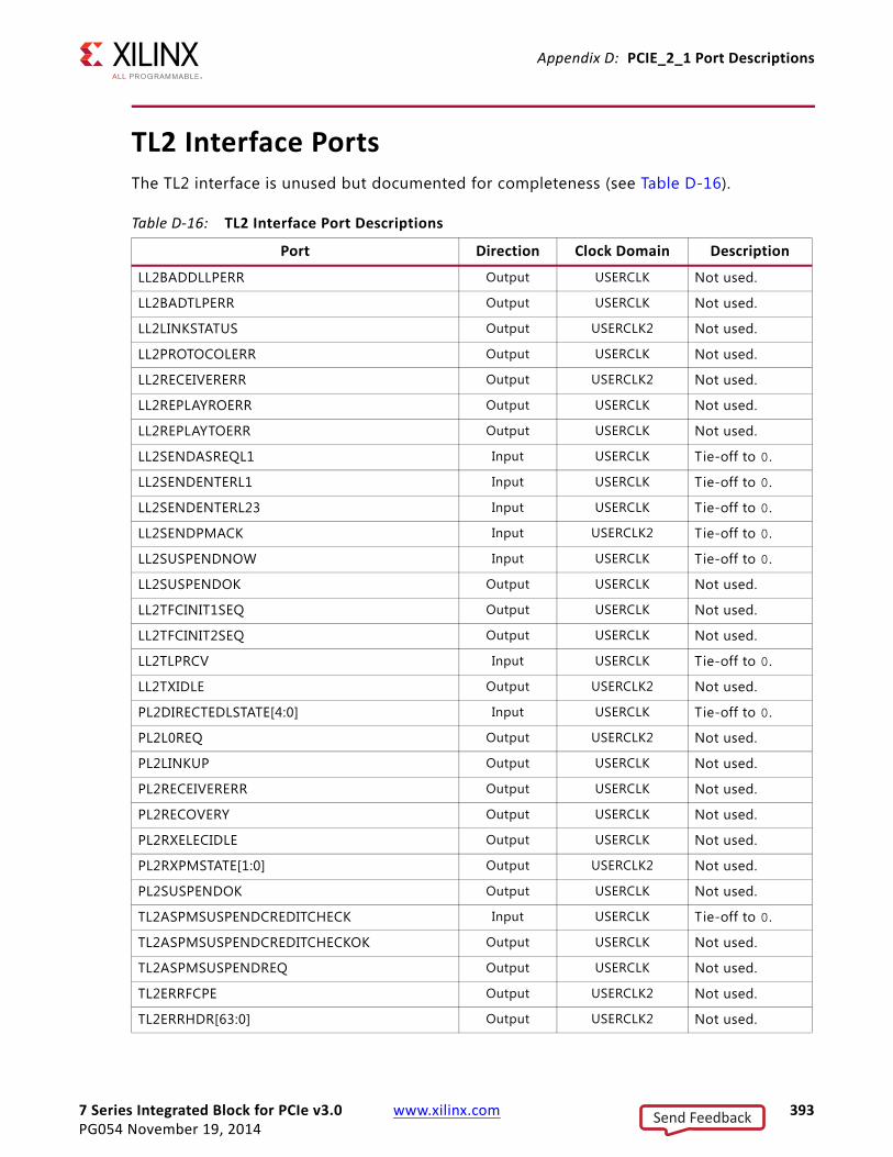
7 Series Integrated Block for PCIe v3.0 www.xilinx.com 393PG054 November 19, 2014
Appendix D: PCIE_2_1 Port Descriptions
TL2 Interface PortsThe TL2 interface is unused but documented for completeness (see Table D-16).
Table D-16: TL2 Interface Port Descriptions
Port Direction Clock Domain Description
LL2BADDLLPERR Output USERCLK Not used.
LL2BADTLPERR Output USERCLK Not used.
LL2LINKSTATUS Output USERCLK2 Not used.
LL2PROTOCOLERR Output USERCLK Not used.
LL2RECEIVERERR Output USERCLK2 Not used.
LL2REPLAYROERR Output USERCLK Not used.
LL2REPLAYTOERR Output USERCLK Not used.
LL2SENDASREQL1 Input USERCLK Tie-off to 0.
LL2SENDENTERL1 Input USERCLK Tie-off to 0.
LL2SENDENTERL23 Input USERCLK Tie-off to 0.
LL2SENDPMACK Input USERCLK2 Tie-off to 0.
LL2SUSPENDNOW Input USERCLK Tie-off to 0.
LL2SUSPENDOK Output USERCLK Not used.
LL2TFCINIT1SEQ Output USERCLK Not used.
LL2TFCINIT2SEQ Output USERCLK Not used.
LL2TLPRCV Input USERCLK Tie-off to 0.
LL2TXIDLE Output USERCLK2 Not used.
PL2DIRECTEDLSTATE[4:0] Input USERCLK Tie-off to 0.
PL2L0REQ Output USERCLK2 Not used.
PL2LINKUP Output USERCLK Not used.
PL2RECEIVERERR Output USERCLK Not used.
PL2RECOVERY Output USERCLK Not used.
PL2RXELECIDLE Output USERCLK Not used.
PL2RXPMSTATE[1:0] Output USERCLK2 Not used.
PL2SUSPENDOK Output USERCLK Not used.
TL2ASPMSUSPENDCREDITCHECK Input USERCLK Tie-off to 0.
TL2ASPMSUSPENDCREDITCHECKOK Output USERCLK Not used.
TL2ASPMSUSPENDREQ Output USERCLK Not used.
TL2ERRFCPE Output USERCLK2 Not used.
TL2ERRHDR[63:0] Output USERCLK2 Not used.
Send Feedback

7 Series Integrated Block for PCIe v3.0 www.xilinx.com 394PG054 November 19, 2014
Appendix D: PCIE_2_1 Port Descriptions
TL2ERRMALFORMED Output USERCLK2 Not used.
TL2ERRRXOVERFLOW Output USERCLK2 Not used.
TL2PPMSUSPENDOK Output USERCLK Not used.
TL2PPMSUSPENDREQ Input USERCLK Tie-off to 0.
TRNRDLLPDATA[31:0] Output USERCLK Not used.
TRNRDLLPSRCRDY[1:0] Output USERCLK Not used.
TRNTDLLPDATA[63:0] Input USERCLK Tie-off to 0.
TRNTDLLPDSTRDY Output USERCLK Not used.
TRNTDLLPSRCRDY Input USERCLK Tie-off to 0.
Table D-16: TL2 Interface Port Descriptions (Cont’d)
Port Direction Clock Domain Description
Send Feedback
7 Series Integrated Block for PCIe v3.0 www.xilinx.com 395PG054 November 19, 2014
Appendix E
Additional Resources and Legal Notices
Xilinx ResourcesFor support resources such as Answers, Documentation, Downloads, and Forums, see Xilinx Support.
ReferencesThis section provides supplemental material useful with this product guide.
1. AMBA AXI4-Stream Protocol Specification
2. PCI-SIG® Specif ications
3. Intel Developer Forum For PCI Express Architecture
4. Virtex-7 FPGA Gen3 Integrated Block for PCI Express Product Guide (PG023)
5. Kintex-7 FPGAs Data Sheet: DC and AC Switching Characteristics (DS182)
6. Virtex-7 FPGAs Data Sheet: DC and Switching Characteristics (DS183)
7. 7 Series FPGAs Configuration User Guide (UG470)
8. Zynq-7000 All Programmable SoC Technical Reference Manual (UG585)
9. Zynq-7000 All Programmable SoC Software Developers Guide (UG821)
10. 7 Series FPGAs SelectIO Resources User Guide (UG471)
11. 7 Series FPGAs Clocking Resources User Guide (UG472)
12. 7 Series FPGAs GTX/GTH Transceivers User Guide (UG476)
13. Vivado Design Suite User Guide: Getting Started (UG910)
14. Vivado Design Suite User Guide: Design with IP (UG896)
15. Vivado Design Suite User Guide: Logic Simulation (UG900)
16. Vivado Design Suite User Guide: Programming and Debugging (UG908)
17. ISE to Vivado Design Suite Migration Methodology Guide (UG911)
Send Feedback
7 Series Integrated Block for PCIe v3.0 www.xilinx.com 396PG054 November 19, 2014
Appendix E: Additional Resources and Legal Notices
18. Vivado Design Suite User Guide: Designing IP Subsystems using IP Integrator (UG994)
19. Vivado Design Suite Tcl Command Reference Guide (UG835)
20. PIPE Mode Simulation Using Integrated Endpoint PCI Express Block in Gen2 x8 Configurations Application Note (XAPP1184)
21. ATX 12V Power Supply Design Guide
Revision HistoryThe following table shows the revision history for this document. runtime
Date Version Revision
11/19/2014 3.0 • Added new Artix and Zynq device support.• Updated the tandem configuration information.• Correction made to the AER_CAP_VERSION[3:0] value.• Clarif ication made to the PIPE Mode Simulations parameter description.• Added support for Cadence Incisive Enterprise Simulator (IES) and
Synopsys Verilog Compiler Simulator (VCS).
10/01/2014 3.0 • Correction to valid values for m_axis_rx_tuser[21:17] receiver interface signal.
• Updated the tandem configuration information.
06/04/2014 3.0 • Added new device support.• Updated tandem configuration information.
04/02/2014 3.0 • Updated device and package information.
12/18/2013 3.0 • Updated for core v3.0.• Updated integrated blocks table for Artix-7 in Product Specification.• Updated logic sharing information in Designing with the Core.• Updated supported core pinouts in Constraining the Core.• Updated parameter and port information in Migrating and Updating
appendix.
Send Feedback

7 Series Integrated Block for PCIe v3.0 www.xilinx.com 397PG054 November 19, 2014
Appendix E: Additional Resources and Legal Notices
Please Read: Important Legal NoticesThe information disclosed to you hereunder (the "Materials") is provided solely for the selection and use of Xilinx products. To the maximum extent permitted by applicable law: (1) Materials are made available "AS IS" and with all faults, Xilinx hereby DISCLAIMS ALL WARRANTIES AND CONDITIONS, EXPRESS, IMPLIED, OR STATUTORY, INCLUDING BUT NOT LIMITED TO WARRANTIES OF
10/02/2013 2.2 • Updated for core v2.2. • Added Vivado IP integrator support.• Added BUFG resource utilization numbers.• Added information about the Shared Logic feature, and the new Share
Logic and Core Interface Parameters options in the Vivado IDE.• Updated the Tandem Configuration section.• Added Simulation, Synthesis and Implementation, and Test Bench chapters. • Reorganized content: moved test bench information from Example Design
chapter to Test Bench chapter, and moved core simulation content into Simulation chapter.
• Updated the example design content.• Added the Transceiver Control and Status Port section to Debugging
appendix.• Added core parameter and port changes to Migrating and Upgrading
appendix.
06/19/2013 2.1 • Updated for core v2.1.• Major updates to the Tandem Configuration section in Chapter 3.• Updated the Directory and File Contents section in Chapter 5.• Added simulation instructions in Chapter 5.
03/20/2013 2.0 • Updated for core v2.0 and for Vivado Design Suite-only support.• Added the PIPE_MMCM_RST_N clocking interface signal.• Updated Clocking in Chapter 3.
12/18/2012 1.2 • Updated for core v1.8, ISE Design Suite 14.4, and Vivado Design Suite 2012.4.
• Updated the available integrated block for PCIe: Table 2-5 and Table 5-1.• Major revisions made to Clocking in Chapter 3.• Updated Chapter 4, Customizing and Generating the Core.
10/16/2012 1.1 • Updated core to v1.7, ISE Design Suite to 14.3, and Vivado Design Suite to 2012.3.
• Added Zynq®-7000 device family support.• Removed XC7V1500T, and XC7A350T.• Added new sections to Chapter 3.• New screenshots and descriptions in Chapter 4.• Added Chapter 6 and Chapter 15.
07/25/2012 1.0 Initial Xilinx release. This document includes support for Vivado Design Suite v2012.2 and ISE Design Suite v14.2 for core version 1.6. This document replaces UG477, 7 Series FPGAs Integrated Block for PCI Express User Guide and DS821, LogiCORE IP 7 Series FPGAs Integrated Block for PCI Express Data Sheet.
Date Version Revision
Send Feedback

7 Series Integrated Block for PCIe v3.0 www.xilinx.com 398PG054 November 19, 2014
Appendix E: Additional Resources and Legal Notices
MERCHANTABILITY, NON-INFRINGEMENT, OR FITNESS FOR ANY PARTICULAR PURPOSE; and (2) Xilinx shall not be liable (whether in contract or tort, including negligence, or under any other theory of liability) for any loss or damage of any kind or nature related to, arising under, or in connection with, the Materials (including your use of the Materials), including for any direct, indirect, special, incidental, or consequential loss or damage (including loss of data, profits, goodwill, or any type of loss or damage suffered as a result of any action brought by a third party) even if such damage or loss was reasonably foreseeable or Xilinx had been advised of the possibility of the same. Xilinx assumes no obligation to correct any errors contained in the Materials or to notify you of updates to the Materials or to product specifications. You may not reproduce, modify, distribute, or publicly display the Materials without prior written consent. Certain products are subject to the terms and conditions of Xilinx's limited warranty, please refer to Xilinx's Terms of Sale which can be viewed at http://www.xilinx.com/legal.htm#tos; IP cores may be subject to warranty and support terms contained in a license issued to you by Xilinx. Xilinx products are not designed or intended to be fail-safe or for use in any application requiring fail-safe performance; you assume sole risk and liability for use of Xilinx products in such critical applications, please refer to Xilinx's Terms of Sale which can be viewed at http://www.xilinx.com/legal.htm#tos.© Copyright 2012 - 2014 Xilinx, Inc. Xilinx, the Xilinx logo, Artix, ISE, Kintex, Spartan, Virtex, Vivado, Zynq, and other designated brands included herein are trademarks of Xilinx in the United States and other countries. PCI, PCIe and PCI Express are trademarks of PCI-SIG and used under license. All other trademarks are the property of their respective owners.
Send Feedback


