Data Device Corporation 105 Wilbur Place Bohemia, New York 11716 631-567-5600 Fax: 631-567-7358 www.ddc-web.com
FOR MORE INFORMATION CONTACT:
Technical Support: 1-800-DDC-5757 ext. 7771
FEATURES
• 7 VA Drive Capability for CT, CDX, or TR Loads
• Double Buffered Transparent Input Latch
• 16-Bit Resolution
• Up to 2 Minute Accuracy
• Power Amplifier Uses Pulsating or DC Supplies
• Built-In-Test (BIT) Output
DESCRIPTION
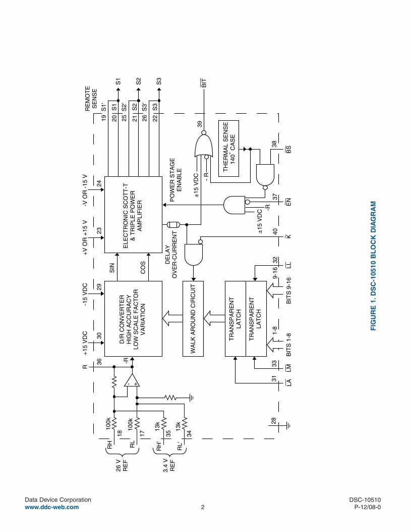
The DSC-10510 is a high power Digital-to-Synchro converter, with 16-bit resolution and up to ±2 minute accuracy. The DSC-10510 is capable of driving multiple Control Transformer (CT), Control Differential Transmitter (CDX) and Torque Receiver (TR) loads up to 7 VA.
The DSC-10510 contains a high accuracy D/R converter, a triple power amplifier stage, a walk-around circuit (to prevent torque receiver hangups), and thermal and over-current protection circuits. The hybrid is protected against overloads, load transients, over-temperature, loss of reference, and power amplifier or DC power supply shutdown.
Microprocessor compatibility is provided through a 16-bit/2-byte double-buffered input latch. Data input is natural binary angle in TTL compatible parallel positive logic format.
Packaged in a 40-pin TDIP, the DSC-10510 features a power stage that may be driven by either a standard ±15 VDC supply or by a pulsating reference supply when used with an optional power transformer. When powered by the reference source, heat dissipation is reduced by 50%.
APPLICATIONS
The DSC-10510 can be used where digitized shaft angle data must be converted to an analog format for driving CT’s, CDX’s, and TR loads. With its double buffered input latches, the DSC-10510 easily interfaces with microprocessor based systems such as flight simulators, flight instrumentation, fire control systems, and flight data computers.
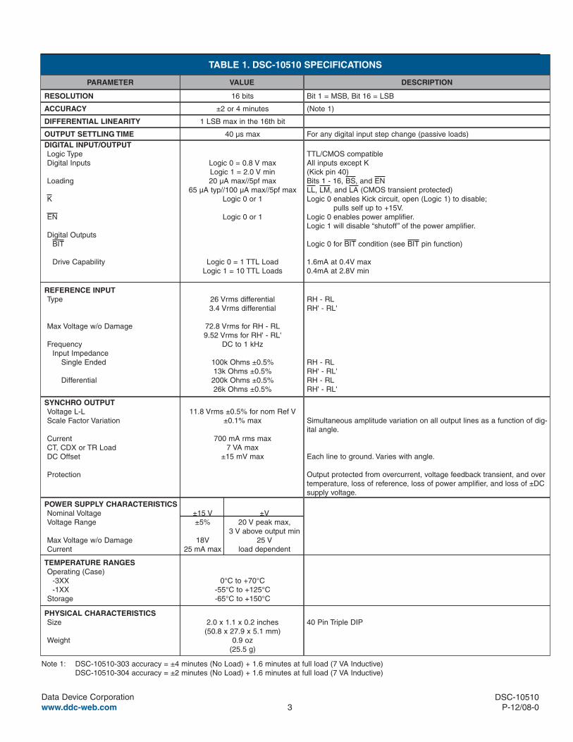
oUTpUT SETTlInG TImE 40 µs max For any digital input step change (passive loads)DIGITal InpUT/oUTpUTLogic TypeDigital Inputs
Loading
K
EN
Digital OutputsBIT
Drive Capability
Logic 0 = 0.8 V maxLogic 1 = 2.0 V min20 µA max//5pf max
65 µA typ//100 µA max//5pf maxLogic 0 or 1
Logic 0 or 1
Logic 0 = 1 TTL LoadLogic 1 = 10 TTL Loads
TTL/CMOS compatible All inputs except K(Kick pin 40)Bits 1 - 16, BS, and ENLL, LM, and LA (CMOS transient protected)Logic 0 enables Kick circuit, open (Logic 1) to disable;
pulls self up to +15V.Logic 0 enables power amplifier.Logic 1 will disable “shutoff” of the power amplifier.
Simultaneous amplitude variation on all output lines as a function of dig-ital angle.
Each line to ground. Varies with angle.
Output protected from overcurrent, voltage feedback transient, and over temperature, loss of reference, loss of power amplifier, and loss of ±DC supply voltage.
powER SUpply ChaRaCTERISTICSNominal VoltageVoltage Range
Max Voltage w/o DamageCurrent
±15 V±5%
18V25 mA max
±V20 V peak max,
3 V above output min25 V
load dependent
TEmpERaTURE RanGESOperating (Case)
-3XX-1XX
Storage
0°C to +70°C-55°C to +125°C-65°C to +150°C
phySICal ChaRaCTERISTICSSize
Weight
2.0 x 1.1 x 0.2 inches(50.8 x 27.9 x 5.1 mm)
0.9 oz(25.5 g)
40 Pin Triple DIP
Note 1: DSC-10510-303 accuracy = ±4 minutes (No Load) + 1.6 minutes at full load (7 VA Inductive) DSC-10510-304 accuracy = ±2 minutes (No Load) + 1.6 minutes at full load (7 VA Inductive)
4Data Device Corporation www.ddc-web.com
DSC-10510P-12/08-0
InTRoDUCTIon
SYSTEM CONSIDERATIONS:
Power Surge at turn onThe output power stages can fully turn on before all the supplies stabilize, when power is initially applied. Multiple D/S converters with substantial loads can cause the system power supply to have difficulty coming up and may even cause the supply to shut down. It is important that the power supply can handle the turn-on surge or that the D/S turn-ons be staggered. Typically, the surge will be twice the max rated draw of the converter.
Power SuPPly cyclingPower supply cycling of the DSC-10510 should follow the guide-lines below to avoid any potential problems.
Strictly maintain proper sequencing of supplies and signals per typical CMOS circuit guidelines:
- Apply power supplies first (+15, -15V and ground).
- Apply digital control signals next.
- Apply analog signals last.
The reverse sequence should be followed during power down of the circuit.
It is also recommended that the KICK pin, if unused, be left in the “No Connection” (N/C) state. The internal pull up will disable the pin (this removes any unnecessary voltages from the convert-er).
torque load ManageMentThe above problems are compounded by the high power levels involved when multiple torque loads (TR) are being driven. In this configuration, power supply fold back problems are common unless the stagger technique is used. The load will also need time to stabilize. On turn-on it is likely that some of output loads will be at a different angle than the D/S output. As the angular difference increases so does the power draw until the difference is 180 degrees. At this point the load impedance drops to Zss and current draw is at a maximum.
PulSating Power SuPPlieSD/S and D/R converters have been designed to operate their output power stages with pulsating power to reduce power dis-sipation and power demand from regulated supplies. Figures 2 and 3 illustrate this technique. The power output stage is only supplied with enough instantaneous voltage to be able to drive the required instantaneous signal level. The AC reference can be full wave rectified and applied to the push-pull output drivers since the output signal is required to be in phase with the AC reference. The supply voltage will be just a few volts more than the output signal and internal power dissipation is minimized.
REFERENCESOURCE
26V rms 400Hz
1
2
3
4
5
6
7
3.4V rms
21.6V rmsC.T.
D1 D2
D3D4
C1
C2
+
+
RL' RH'
+V
GND
-V
S1
S2
S3
DIGITALINPUT
±15VDC
DSC10510
S1
S1'
S2
S2'
S3
S3'
T1
42359
NOTES: PARTS LIST FOR 400Hz D1, D2, D3, D4 = 1N4245 C1 AND C2 = 47µF, 35V DC CAPACITOR
FIGURE 2. TypICal ConnECTIon DIaGRam UTIlIzInG pUlSaTInG powER SoURCE
FIGURE 3. pUlSaTInG powER SUpply VolTaGE waVEFoRmS
+v
- v
+DC SUPPLY LEVEL
-DC SUPPLY LEVEL
POSITIVE PULSATINGSUPPLY VOLTAGE
NEGATIVE PULSATINGSUPPLY VOLTAGE
AMPLIFIER OUTPUTVOLTAGE ENVELOPE
5Data Device Corporation www.ddc-web.com
DSC-10510P-12/08-0
therMal conSiderationS Power dissipation in D/S and D/R circuits is dependent on the load, whether active (TR) or passive (CT or CDX), and the power supply, whether DC or pulsating. With inductive loads virtually all the power consumed will have to be dissipated in the output amplifiers. This can require considerable care in heat sinking.
example:For illustrative purposes the following thermal calculations are made using the DSC-10510’s specifications. The DSC-10510 has a 7 VA drive capability for CT, CDX, or TR loads.
Simplest case first: passive Inductive load and ±15 Volt DC power stage supplies (as shown in Figure 2). The power dis-sipated in the power stage can be calculated by taking the inte-gral of the instantaneous current multiplied by the voltage differ-ence from the DC supply that supplies the current and instanta-neous output voltage over one cycle of the reference. For an inductive load this is a rather tedious calculation. Instead take the difference between the power input from the DC supplies minus the power delivered to the load. An actual synchro load is highly inductive with a Q of 4-6; therefore assume that it is purely reac-tive. The power out, then, is 0 Watts. As a worst case scenario, also assume the load is the full 7 VA, the converter’s rated load.
The VA delivered to the load is independent of the angle but the voltage across the synchro varies with the angle from a high of 11.8 Volts line-to-line (L-L) to a low of 10.2 V L-L (Note 1). The maximum current therefore is 7VA/10.2 V = 0.68 A rms. The
output is L-L push-pull, that is, all the current flows from the positive supply out to the load and back to the negative supply. The power input is the DC voltage times the average current or 30 V x (0.68 A x 0.635/0.707) [avg/rms] = 18.32 Watts.
note 1: The DSC-10510 has an 11.8 VL-L synchro output. In this case, we use 11.8V x sin 120° = 11.8V x .866 = 10.2 VL-L. To calculate the load use Zso. Zso is the impedance between one of the three stator wires and the other two shorted together with the rotor open circuit. VL-L x .866 is the voltage that would result from this configuration.
The power dissipated by the output driver stage is over 18 Watts shared by the six power transistors. Since one synchro line sup-plies all the current while the other two share it equally, one will dissipate 2/3 of the power and the other two will each dissipate 1/3. There are 2 transistors per power stage so each of the two transistors dissipates 1/3 of the power and the other transistors dissipate 1/6 of the power. This results in a maximum power in any one transistor of 1/3 x 18.32 W = 6.04 Watts. The heat rise from the junction to the outside of the package, assuming a ther-mal impedance of 4°C per watt = 24.16°C. At an operating case temperature of 125°C the maximum junction temperature will be 149.16°C.
The other extreme condition to consider is when the output volt-age is 11.8 V. The current then will be 0.42 Amps and the power will be 30 x (0.42A x 0.635/0.707) = 11.32 Watts. A similar calcu-lation will show the maximum power per transistor to be 2.3 Watts. This is much less than when the output voltage is 10.2 V.
For pulsating Supplies the analysis is much more difficult. Calculations for a purely reactive load with DC supplies equal to the output voltage peak vs. pulsating supplies with a supply volt-age equal to the output voltage yield an exact halving of the power dissipated. At light loads the pulsating supplies approxi-mate DC supplies and at heavy loads, which is the worst case, they approximate a pulsating supply as shown in Figure 4. Advantages of the pulsating supply technique are:
+15VDC
-15VDC
LIGHT LOAD
HEAVY LOAD
FIGURE 4. loaDED waVEFoRmS
REF IN D/S
R2=1 1/3 R1=2/3
REFZSO=8.6
NOTES: R1 + R2 ZSS
3-WIRE SYNCHRO 2-WIRE REF
ACTIVE LOAD
FIGURE 5. EqUIValEnT 2-wIRE CIRCUIT FIGURE 6. ToRqUE SySTEm
R1 R2 R1R2
REF REF
TORQUE TRANSMITTER TORQUE RECEIVER
6Data Device Corporation www.ddc-web.com
DSC-10510P-12/08-0
• Reduced load on the regulated ±15 VDC supplies
• Halving of the total power
• Simplified power dissipation management
actiVe loadActive loads (torque receivers) make it more difficult to calculate power dissipation. The load is composed of an active part and a passive part. Figure 5 illustrates the equivalent two wire circuit. At null, when the torque receiver’s shaft rotates to the angle that minimizes the current in R2, the power dissipated is at its lowest. The typical ratio of Zso/Zss = 4.3. For the maximum specified load of Zss = 2 ohm, the Zso = 2 x 4.3 = 8.6 ohms. Also, the typical ratio of R2/R1= 2.
In synchro systems with a torque transmitter driving a torque receiver, the actual line impedances are as shown in Figure 6. The torque transmitter and torque receiver are electrically identi-cal, so that the total line impedance is double that of Figure 5. The torque system is designed to operate this way. The higher the total line impedances, the lower the current flow at null and the lower the power dissipation. It is recommended that with
torque loads, discrete resistors be used as shown in Figures 7 and 8.
A torque load is normally at null. Once the torque receiver nulls at power turn on, the digital commands to the D/S are typically in smaller angular steps, so the torque system is always at or near null. Large digital steps, load disturbances, a stuck torque receiv-er or one synchro line open, however, cause an off null condi-tion.
At null the load current could be zero (See Figure 9 ). If Vac = Vab, both in magnitude and phase, then, when “a” is connected to “b,” no current will flow. Pick C1 and C2 to match the phase lead of R1 – Zso. In practice this ideal situation is not realized. The input to output transformation ratio of torque receivers is specified at 2% and the turns ratio at 0.4%. The in-phase current flow due to this nominal output voltage (10.2 V) multiplied by the % error (2.4/100) divided by total resistance (4 Ohms) = 61mA. A phase lead mismatch between the torque receiver and the converter of 1 degree results in a quadrature current of 10.2 V x sin 1°/4 Ohms = 44.5 mA. Total current is the phaser sum 61 + 44.5 = 75.5 mA. Power dissipation is 30 VDC x 75.5 mA rms x 0.9 (avg/rms) = 2.04 Watts. Since this is a light load condition, even pulsating supplies would be approximating DC supplies.
The off null condition power dissipation is quite different. Actual synchros have no current limiting, so the circuit current is the current that the circuit conditions demand. The worst case would be for a 180 degree error between the two synchros as shown in Figure 10. For this condition the two equivalent voltage sources are 10.2 V opposing. The current is (10.2 x 2) / 4 = 5.1 A in phase.
The power dissipated in the converter is the power supplied by the ±15 VDC supplies minus the power delivered to the load (30 V x 5.1 A x 0.9) - (10.2 V x 5.1 A) = 87.7 Watts for DC supplies. This requires a large power supply and high wattage resistors.
FIGURE 7. D/S EqUIValEnT
REF IN
RH
RL
D/S
2 11/3 2/3
ZSO=8.6 REF
TORQUE LOAD WITH DISCRETE EXTERNAL RESISTOR
1.33
1.33
1.33
S1
S2
S3
RH
RL
S1
S2
S3
D/S TRREF IN REF
FIGURE 8. D/S - aCTUal hook-Up
2
RH
RL
A
D/S
1 1/3 2/3
REFZso=8.6
B
C
REF IN
C1
C2
R1
FIGURE 9. IDEal nUll ConDITIon
7Data Device Corporation www.ddc-web.com
DSC-10510P-12/08-0
The converter output current is typically limited (in the DSC-10510 case to 0.8 A peak). This limits the power supply to more reasonable values but introduces another problem – the torque receiver can hang up in a continuous current limited condition at a false stable null. The DSC-10510 has special circuits that sense this continuous current overload condition and sends a momentary 45° “kick” to the torque receiver thus knocking it off the false null. The torque receiver will then swing to the correct angle and properly null. If the torque receiver is stuck it will not be able to swing off the over-current condition. In this case the converter will send a BIT signal when the case temperature
exceeds 140°C. This BIT signal can be used to shut down the output power stage.
An additional advantage of using pulsating power supplies is that the loss of reference when driving torque loads is fail safe. The load will pump up the ±V voltage through the power stage clamp diodes and the loss of the reference detector will disable the power stage. The power stage will be turned off with the required power supply voltages. The pulsating power supply diodes will isolate the pumped up pulsating supplies from the reference. If the DC power supplies are to be used for the power stage, and there is a possibility of the DC supplies being off while the refer-ence to the torque receiver is on, then the protection circuitry shown in Figure 11 is highly recommended.
A remote sense feature is incorporated in DDC’s DSC-10510 hybrid digital-to-synchro converter. Rated at 7 VA, it offers accu-racies to ±2 minutes of arc at the load. This remote sense feature operates just as other precision sources do. A separate line is run to each leg of the synchro (in addition to the drive line) to sense the voltage actually appearing on the load. This is then used to regulate the output based on load voltage rather than converter output voltage. This feature is very useful in driving heavy passive loads in precision systems.
2
D/S
2
10.2V
+15V
10.2V
- 15V
FIGURE 10. woRST CaSE 180° ERRoR
D/S
+V
-V
+
-V
+15VDC
-15VDC
FIGURE 11. pRoTECTIon CIRCUITRy
8Data Device Corporation www.ddc-web.com
DSC-10510P-12/08-0
Data Changing Data Stable
125 nS min. 125 nS min.
125 nS min. 125 nS min.
200 nS min.
200 nS min.
200 nS min.
LL
LM
LA
DATA
Bits (9-16)
Bits (1-8)
200 nS min.
LA, LM, LLTransparent = HiLatched = Lo
FIGURE 12B . ll, lm, la TImInG DIaGRam (8 BIT)
FIGURE 12a. ll, lm, la TImInG DIaGRam (16 BIT)
200 nS min.
TRANSPARENT
LATCHED
DATA 1-16 BITS
125 nS min.
Data Changing Data Stable
With LA set Lo = 125 nS min.
With LL, LM, LA tied together = 200nS min.
LL, LM, LA all tied together
9Data Device Corporation www.ddc-web.com
DSC-10510P-12/08-0
0.900(22.86)
0.018 ±0.002(0.46 ±0.05)
DIA PIN
SIDE VIEWBOTTOM VIEW
2.14(54.36)
19 EQ. SP.0.100 = 1.9
TOL. NONCUM(2.5 = 48.3)
1.140(28.96)
0.200 MAX(5.08)
0.17 MIN(4.32)
20 21
1 40
0.120 ±0.002(3.05 ±0.05)
0.120 ±0.002(3.05 ±0.05)
notes:1. Dimensions are in inches (millimeters).2. Lead identification numbers for reference only.3. Lead cluster shall be centered within ±0.10 of outline dimensions.
Lead spacing dimensions apply only at seating plane.4. Pin material meets solderability requirements of MIL-PRF-38534
31 LA 2nd Latch All Enable. Input enables dual latch.
32 LL 1st Latch LSBs Enable. Enables bits 9 - 16
33 LM 1st Latch MSBs Enable. Enables bits 1 - 8
34 RL' 3.4 Vrms Reference Low Input
35 RH' 3.4 Vrms Reference High Input
36 -R (TP) No connection. Factory test point.
37 ENPower stage enable input allows for digital shutdown of power stage when this pin is set to Logic 1.
38 BSBattle Short Input. Logic 0 overrides over tempera-ture protection.
39 BIT
Built-In-Test Output. Logic 0 when loss of refer-ence, loss of ±15 VDC supply, case temperature of +140°C, or an output over-current has been detect-ed. Loss of reference, loss of ±15 VDC supply or case temperature of +140°C will disable the power-o u t p u t s t a g e .
40 KKick. Input used for reducing excessive current flow in torque receiver loads at false null.
Table 3.aNGleS IN DeGReeS CROSS ReFeReNCeD TO a 16-bIT DIGITal WORD
0
10Data Device Corporation www.ddc-web.com
DSC-10510P-12/08-0
FIGURE 14. DDC 42359 oUTlInE DRawInG (26 VolT powER TRanSFoRmER)
.725 MAX.
1.435 ±� .010 .183 ± .015
.100 (TYP)
4 EQUAL SPACES @ .100 = .400 (TOTAL NON-CUM.)
4-40 8 THREADS THREADED INSERT (2 PLACES)
.700
.300
1.00 ± .015
.150 ± .015
.128 REF. 1.545
1.800 ± .015
.055 (TYP)
.190 MIN.
.020 ± .002 DIA. (TYP)
NOTE: FOR REFERENCE ONLY, CONTACT BETA TRANSFORMER CORPORATION FOR SPEC DETAILS.
4
1
2
3
56
7
SC H E M A T I C
11Data Device Corporation www.ddc-web.com
DSC-10510P-12/08-0
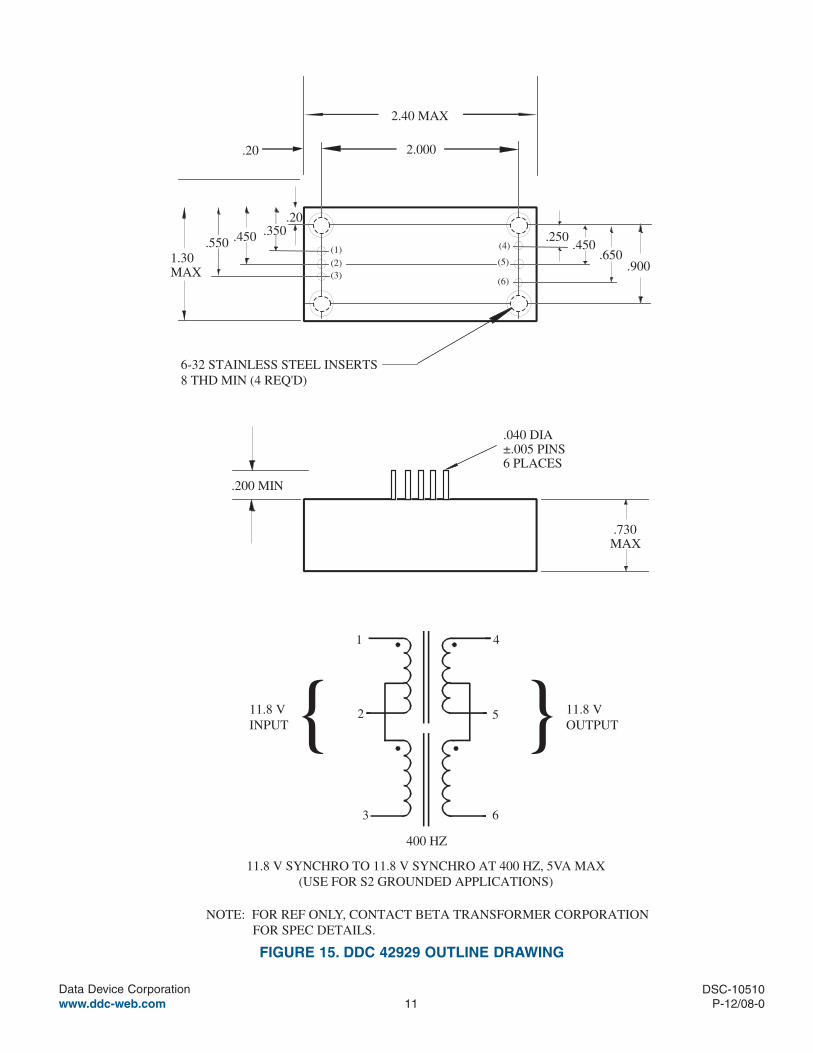
FIGURE 15. DDC 42929 oUTlInE DRawInG
.040 DIA ±.005 PINS
6 PLACES
.200 MIN
.900
.20
1.30 MAX
2.40 MAX
2.000
.250
.650
.20
(5)
(6)
(4)
(3)
(1) (2)
.450 .350 .450 .550
MAX .730
4
5
6
1
3
2 }}11.8 V INPUT
11.8 V OUTPUT
6-32 STAINLESS STEEL INSERTS 8 THD MIN (4 REQ'D)
400 HZ
11.8 V SYNCHRO TO 11.8 V SYNCHRO AT 400 HZ, 5VA MAX (USE FOR S2 GROUNDED APPLICATIONS)
NOTE: FOR REF ONLY, CONTACT BETA TRANSFORMER CORPORATION FOR SPEC DETAILS.
12Data Device Corporation www.ddc-web.com
DSC-10510P-12/08-0
FIGURE 16. DDC 41402 oUTlInE DRawInG
.040 DI A±�.005 PI NS 6 PLACES
.200 MI N
.900
.20
1.30 MA X
2.40 MA X
2.000
.250
.650
6-32 INSERT 8 T HD M IN4 PLACES
.20
(5)
(6)
(4)
(3)
(1) (2)
.450.350 .450 .550
MA X .730
5
6
7
1
4
2}11.8 V�INPUT } 90 V @ 5VA MAX�
OUTPUT
400 HZ
NOTE: FOR REF ONLY, CONTACT BETA TRANSFORMER CORPORATION� FOR SPEC DETAILS.
�
13Data Device Corporation www.ddc-web.com
DSC-10510P-12/08-0
oRDERInG InFoRmaTIonDSC-10510-xxxx Supplemental process Requirements: S = Pre-Cap Source Inspection L = Pull Test Q = Pull Test and Pre-Cap Inspection Blank = None of the Above
accuracy: 3 = ±4 minutes (No Load) + 1.6 minutes at full Load (7VA Inductive) 4 = ±2 minutes (No Load) + 1.6 minutes at full Load (7VA Inductive)
process Requirements: 0 = Standard DDC Processing, no Burn-In (See table below.) 1 = MIL-PRF-38534 Compliant (Note 3) 2 = B (Note 1) 3 = MIL-PRF-38534 Compliant with PIND Testing (Note 3) 4 = MIL-PRF-38534 Compliant with Solder Dip (Note 3) 5 = MIL-PRF-38534 Compliant with PIND Testing and Solder Dip (Note 3) 6 = B (Note 1) with PIND Testing 7 = B (Note 1) with Solder Dip 8 = B (Note 1) with PIND Testing and Solder Dip 9 = Standard DDC Processing with Solder Dip, no Burn-In (See table below.)
Temperature Grade/Data Requirements: 1 = -55°C to +125°C 2 = -40°C to +85°C 3 = 0°C to +70°C 4 = -55°C to +125°C with Variables Test Data 5 = -40°C to +85°C with Variables Test Data 8 = 0°C to +70°C with Variables Test Data
TRanSFoRmERS
1) Optional Power Transformer, DDC P/N 42359 (See Figure 2 & 14) 2) For S2 Grounded Applications, use Transformer DDC P/N 42929 (Figure 15) Synchro to Synchro 11.8v TO 11.8v 400Hz 3) Synchro 11.8v to Synchro 90v, 400Hz 5 VA max, see Beta Scott-T #41402 (Figure 16). Notes: 1. Standard DDC Processing with burn-in and full temperature test—see table below. 2. These products contain tin-lead solder finish as applicable to solder dip requirements. 3. MIL-PRF-38534 product grading is designated with the following dash numbers: Class H is a -11X, 13X, 14X, 15X, 41X, 43X, 44X, 45X Class G is a -21X, 23X, 24X, 25X, 51X, 53X, 54X, 55X Class D is a -31X, 33X, 34X, 35X, 81X, 83X, 84X, 85X
TABLE 11015 (note 1), 1030 (note 2)BURN-IN
Notes:1. For Process Requirement "B" (refer to ordering information), devices may be non-compliant with MIL-STD-883, Test Method 1015, Paragraph 3.2. Contact factory for details.2. When applicable.
3000g2001CONSTANT ACCELERATION
C1010TEMPERATURE CYCLE
A and C1014SEAL
—2009, 2010, 2017, and 2032INSPECTION
ConDITIon(S)mEThoD(S)
mIl-STD-883TEST
STanDaRD DDC pRoCESSInGFoR hyBRID anD monolIThIC hERmETIC pRoDUCTS
14P-12/08-0 PRINTED IN THE U.S.A.
The information in this data sheet is believed to be accurate; however, no responsibility is assumed by Data Device Corporation for its use, and no license or rights are
granted by implication or otherwise in connection therewith. Specifications are subject to change without notice.
Please visit our web site at www.ddc-web.com for the latest information.
105 Wilbur Place, Bohemia, New York, U.S.A. 11716-2426
For Technical Support - 1-800-DDC-5757 ext. 7771
headquarters, n.y., U.S.a. - Tel: (631) 567-5600, Fax: (631) 567-7358 United kingdom - Tel: +44-(0)1635-811140, Fax: +44-(0)1635-32264 France - Tel: +33-(0)1-41-16-3424, Fax: +33-(0)1-41-16-3425 Germany - Tel: +49-(0)8141-349-087, Fax: +49-(0)8141-349-089 Japan - Tel: +81-(0)3-3814-7688, Fax: +81-(0)3-3814-7689 world wide web - http://www.ddc-web.com
DATA DEVICE CORPORATIONREGISTERED TO ISO 9001:2000
FILE NO. A5976
RE
G ISTERED FIRM
®U
RECORD OF CHANGE
For DSC-10510 Data Sheet
Revision Date Pages Description P 12/2008 3 Added 100µA max to Table 1.