Page 1
70-MHz IF 10-MHz bandwidth bandpass RD modulatorfor WCDMA applications
Herve Caracciolo • Edoardo Bonizzoni •
Piero Malcovati • Franco Maloberti
Received: 15 June 2011 / Revised: 23 September 2011 / Accepted: 24 September 2011 / Published online: 4 October 2011
� Springer Science+Business Media, LLC 2011
Abstract A MASH bandpass RD modulator for wide-
band code division multiple access (WCDMA) applications
is presented. The signal bandwidth of the proposed mod-
ulator is 10 MHz centered around an intermediate fre-
quency (IF) of 70.5 MHz. Two two-path second-order
bandpass RD modulators make the MASH architecture,
which realizes a noise transfer function with four couples
of complex conjugate zeros. The proposed circuit, fabri-
cated with a 0.18 lm CMOS technology, uses a sampling
frequency of 180 MHz to obtain a resolution of about
12 bits in the 10 MHz bandwidth around the IF. The
measured modulator power consumption is 95 mW with a
supply voltage of 1.8 V. The achieved figure-of-merit
(FoMBP) is 0.37 pJ/conversion-level.
Keywords Analog-to-digital conversion � Sigma-delta
modulation � Bandpass
1 Introduction
In modern communication systems, the direct conversion
into the digital domain of a signal at an intermediate fre-
quency (IF), typically in the range 40� 100 MHz, is
becoming quite popular. These communication standards
foresee wide signal bandwidths (5� 10 MHz) while
requiring medium-high resolution (10–14 bits). High-res-
olution Nyquist-rate analog-to-digital converters (ADCs)
with sampling-rate embracing the IF interval consume
significant power, thus making their use affordable only in
base stations. For portable applications, solutions based on
bandpass RD modulators, either with continuous-time and
sampled-data implementations, are preferable because they
reduce power consumption [1–9].
This paper describes the design of a bandpass RDmodulator for wideband code division multiple access
(WCDMA) applications. The considered signal bandwidth
is 10 MHz centered around an IF equal to 70.5 MHz. The
proposed bandpass RD modulator is based on a multi-stage
noise shaping (MASH) architecture which realizes a noise
transfer function (NTF) with four couples of complex
conjugate zeros around the unity circle. The MASH
structure consists of two second-order bandpass RD mod-
ulators, each implemented with a two-path architecture and
cross-coupled integrators. The two-path scheme allows
reducing the power consumption and easily implements the
desired NTF zeros. The RD modulator works with a sam-
pling frequency (fs) of 180 MHz, so that each path runs at
fs/2 = 90 MHz. The proposed RD modulator, fabricated
using a 0.18 lm CMOS technology, achieves a resolution
of about 12 bits consuming 95 mW.
The paper is organized as follows. Section 2 describes
the modulator architecture while Section 3 presents the
behavioral level study. Section 4 discusses the circuit
H. Caracciolo � E. Bonizzoni (&) � F. Maloberti
Department of Electronics, University of Pavia, Via Ferrata, 1,
27100 Pavia, Italy
e-mail: [email protected]
H. Caracciolo
e-mail: [email protected]
F. Maloberti
e-mail: [email protected]
P. Malcovati
Department of Electrical Engineering, University of Pavia,
Via Ferrata, 1, 27100 Pavia, Italy
e-mail: [email protected]
123
Analog Integr Circ Sig Process (2012) 71:411–419
DOI 10.1007/s10470-011-9795-2
Page 2
implementation details and Section 5 illustrates the mea-
surement results. Finally, Section 6 draws some conclusions.
2 Proposed bandpass RD modulator architecture
The proposed MASH architecture consists of two second-
order bandpass RD modulators. Each second-order modu-
lator gives rise to two couples of complex conjugate zeros
in the NTF.
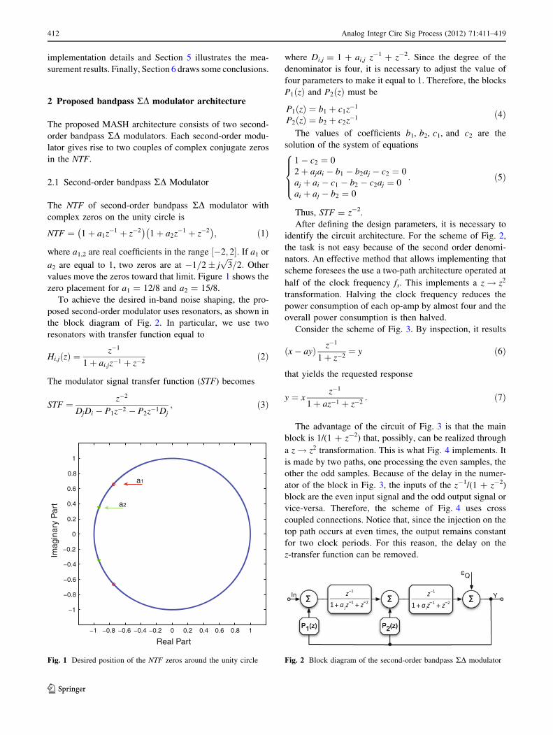
2.1 Second-order bandpass RD Modulator
The NTF of second-order bandpass RD modulator with
complex zeros on the unity circle is
NTF ¼ 1þ a1z�1 þ z�2� �
1þ a2z�1 þ z�2� �
; ð1Þ
where a1,2 are real coefficients in the range �2; 2½ �: If a1 or
a2 are equal to 1, two zeros are at �1=2� jffiffiffi3p
=2: Other
values move the zeros toward that limit. Figure 1 shows the
zero placement for a1 = 12/8 and a2 = 15/8.
To achieve the desired in-band noise shaping, the pro-
posed second-order modulator uses resonators, as shown in
the block diagram of Fig. 2. In particular, we use two
resonators with transfer function equal to
Hi;j zð Þ ¼ z�1
1þ ai;jz�1 þ z�2ð2Þ
The modulator signal transfer function (STF) becomes
STF ¼ z�2
DjDi � P1z�2 � P2z�1Dj; ð3Þ
where Di,j = 1 ? ai,j z-1 ? z-2. Since the degree of the
denominator is four, it is necessary to adjust the value of
four parameters to make it equal to 1. Therefore, the blocks
P1 zð Þ and P2 zð Þ must be
P1 zð Þ ¼ b1 þ c1z�1
P2 zð Þ ¼ b2 þ c2z�1 ð4Þ
The values of coefficients b1, b2, c1, and c2 are the
solution of the system of equations
1� c2 ¼ 0
2þ ajai � b1 � b2aj � c2 ¼ 0
aj þ ai � c1 � b2 � c2aj ¼ 0
ai þ aj � b2 ¼ 0
8>><
>>:: ð5Þ
Thus, STF = z-2.
After defining the design parameters, it is necessary to
identify the circuit architecture. For the scheme of Fig. 2,
the task is not easy because of the second order denomi-
nators. An effective method that allows implementing that
scheme foresees the use a two-path architecture operated at
half of the clock frequency fs. This implements a z! z2
transformation. Halving the clock frequency reduces the
power consumption of each op-amp by almost four and the
overall power consumption is then halved.
Consider the scheme of Fig. 3. By inspection, it results
ðx� ayÞ z�1
1þ z�2¼ y ð6Þ
that yields the requested response
y ¼ xz�1
1þ az�1 þ z�2: ð7Þ
The advantage of the circuit of Fig. 3 is that the main
block is 1/(1 ? z-2) that, possibly, can be realized through
a z! z2 transformation. This is what Fig. 4 implements. It
is made by two paths, one processing the even samples, the
other the odd samples. Because of the delay in the numer-
ator of the block in Fig. 3, the inputs of the z-1/(1 ? z-2)
block are the even input signal and the odd output signal or
vice-versa. Therefore, the scheme of Fig. 4 uses cross
coupled connections. Notice that, since the injection on the
top path occurs at even times, the output remains constant
for two clock periods. For this reason, the delay on the
z-transfer function can be removed.
−1 −0.8 −0.6 −0.4 −0.2 0 0.2 0.4 0.6 0.8 1
−1
−0.8
−0.6
−0.4
−0.2
0
0.2
0.4
0.6
0.8
1
Real Part
Imag
inar
y P
art
a1
a2
Fig. 1 Desired position of the NTF zeros around the unity circle Fig. 2 Block diagram of the second-order bandpass RD modulator
412 Analog Integr Circ Sig Process (2012) 71:411–419
123
Page 3
The use of two choppers and square wave modulators in
each path implements the block of Fig. 4 [10], as shown in
Fig. 5.
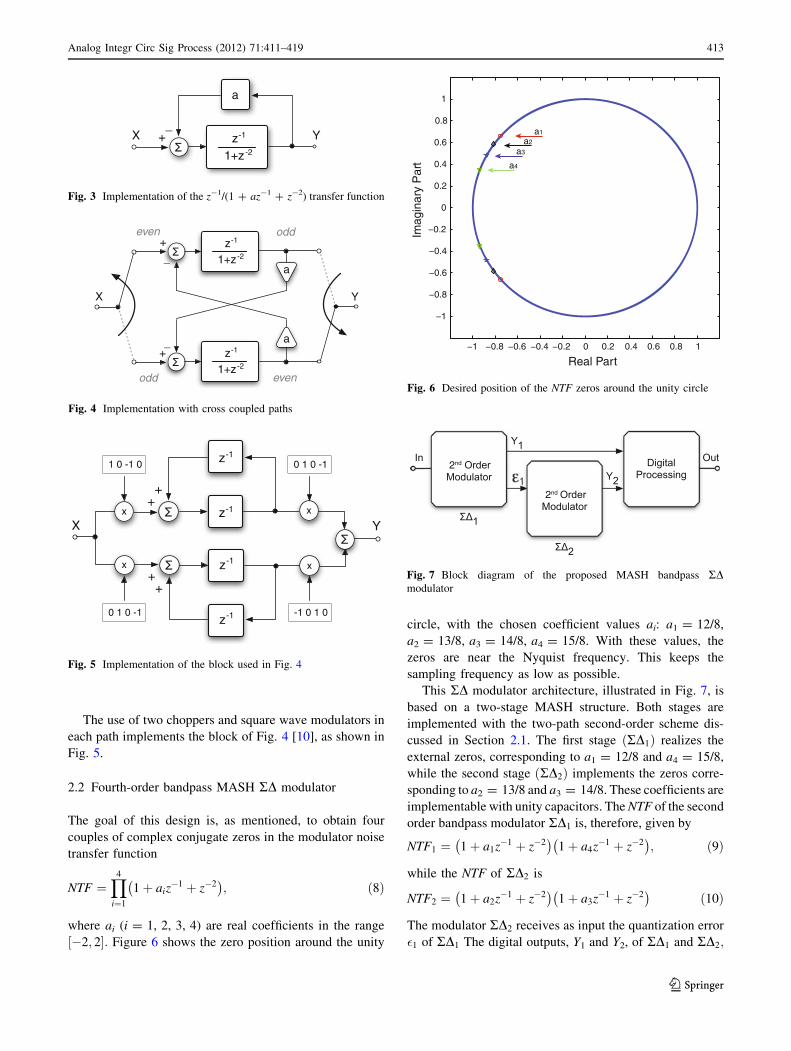
2.2 Fourth-order bandpass MASH RD modulator
The goal of this design is, as mentioned, to obtain four
couples of complex conjugate zeros in the modulator noise
transfer function
NTF ¼Y4
i¼1
1þ aiz�1 þ z�2
� �; ð8Þ
where ai (i = 1, 2, 3, 4) are real coefficients in the range
�2; 2½ �: Figure 6 shows the zero position around the unity
circle, with the chosen coefficient values ai: a1 = 12/8,
a2 = 13/8, a3 = 14/8, a4 = 15/8. With these values, the
zeros are near the Nyquist frequency. This keeps the
sampling frequency as low as possible.
This RD modulator architecture, illustrated in Fig. 7, is
based on a two-stage MASH structure. Both stages are
implemented with the two-path second-order scheme dis-
cussed in Section 2.1. The first stage ðRD1Þ realizes the
external zeros, corresponding to a1 = 12/8 and a4 = 15/8,
while the second stage ðRD2Þ implements the zeros corre-
sponding to a2 = 13/8 and a3 = 14/8. These coefficients are
implementable with unity capacitors. The NTF of the second
order bandpass modulator RD1 is, therefore, given by
NTF1 ¼ 1þ a1z�1 þ z�2� �
1þ a4z�1 þ z�2� �
; ð9Þ
while the NTF of RD2 is
NTF2 ¼ 1þ a2z�1 þ z�2� �
1þ a3z�1 þ z�2� �
ð10Þ
The modulator RD2 receives as input the quantization error
�1 of RD1 The digital outputs, Y1 and Y2, of RD1 and RD2;
z-1
1+z-2
X Y
a
_+
Fig. 3 Implementation of the z-1/(1 ? az-1 ? z-2) transfer function
z-1
1+z-2
z-1
1+z-2
a
X
a
Y
even
evenodd
odd+
+_
_
Fig. 4 Implementation with cross coupled paths
++
z-1
z-1 xx
++
z-1
z-1 xx
1 0 -1 0 0 1 0 -1
0 1 0 -1 -1 0 1 0
X Y
Fig. 5 Implementation of the block used in Fig. 4
−1 −0.8 −0.6 −0.4 −0.2 0 0.2 0.4 0.6 0.8 1
−1
−0.8
−0.6
−0.4
−0.2
0
0.2
0.4
0.6
0.8
1
Real Part
raP
yranigamI
t
a1
a2
a3
a4
Fig. 6 Desired position of the NTF zeros around the unity circle
Fig. 7 Block diagram of the proposed MASH bandpass RDmodulator
Analog Integr Circ Sig Process (2012) 71:411–419 413
123
Page 4
respectively, are processed by a digital filter that cancels
the quantization error of RD1 and realizes the overall NTF
given by (8). Since the outputs of RD1 and RD2 are
Y1 ¼ In � STF1 þ �1 � NTF1
Y2 ¼ �1 � STF2 þ �2 � NTF2
�; ð11Þ
respectively, where STF1 = STF2 = z-2, the digital filter
implements the function
Out ¼ Y1 � z�2 � Y2 � NTF1: ð12Þ
The result cancels the quantization error of RD1 shaped by
NTF1 and gives rise to the desired output, given by
Out ¼ In � z�4 þ �2 �Y4
i¼1
1þ aiz�1 þ z�2
� �: ð13Þ
3 Behavioral level study
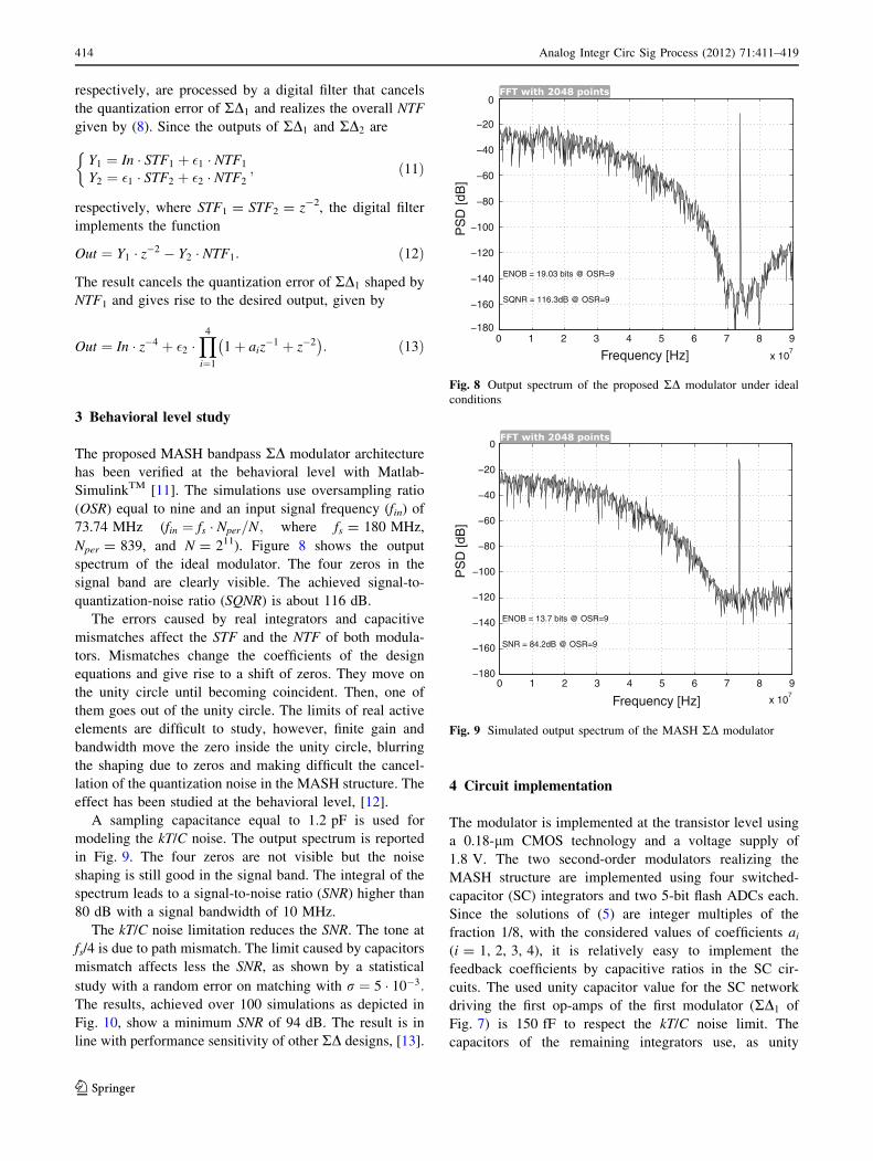
The proposed MASH bandpass RD modulator architecture
has been verified at the behavioral level with Matlab-
SimulinkTM [11]. The simulations use oversampling ratio
(OSR) equal to nine and an input signal frequency (fin) of
73.74 MHz (fin ¼ fs � Nper=N; where fs = 180 MHz,
Nper = 839, and N = 211). Figure 8 shows the output
spectrum of the ideal modulator. The four zeros in the
signal band are clearly visible. The achieved signal-to-
quantization-noise ratio (SQNR) is about 116 dB.
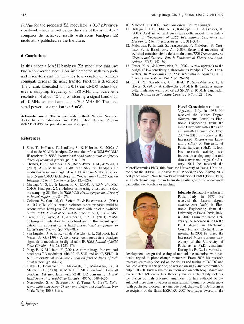
The errors caused by real integrators and capacitive
mismatches affect the STF and the NTF of both modula-
tors. Mismatches change the coefficients of the design
equations and give rise to a shift of zeros. They move on
the unity circle until becoming coincident. Then, one of
them goes out of the unity circle. The limits of real active
elements are difficult to study, however, finite gain and
bandwidth move the zero inside the unity circle, blurring
the shaping due to zeros and making difficult the cancel-
lation of the quantization noise in the MASH structure. The
effect has been studied at the behavioral level, [12].
A sampling capacitance equal to 1.2 pF is used for
modeling the kT/C noise. The output spectrum is reported
in Fig. 9. The four zeros are not visible but the noise
shaping is still good in the signal band. The integral of the
spectrum leads to a signal-to-noise ratio (SNR) higher than
80 dB with a signal bandwidth of 10 MHz.
The kT/C noise limitation reduces the SNR. The tone at
fs/4 is due to path mismatch. The limit caused by capacitors
mismatch affects less the SNR, as shown by a statistical
study with a random error on matching with r ¼ 5 � 10�3:
The results, achieved over 100 simulations as depicted in
Fig. 10, show a minimum SNR of 94 dB. The result is in
line with performance sensitivity of other RD designs, [13].
4 Circuit implementation
The modulator is implemented at the transistor level using
a 0.18-lm CMOS technology and a voltage supply of
1.8 V. The two second-order modulators realizing the
MASH structure are implemented using four switched-
capacitor (SC) integrators and two 5-bit flash ADCs each.
Since the solutions of (5) are integer multiples of the
fraction 1/8, with the considered values of coefficients ai
(i = 1, 2, 3, 4), it is relatively easy to implement the
feedback coefficients by capacitive ratios in the SC cir-
cuits. The used unity capacitor value for the SC network
driving the first op-amps of the first modulator (RD1 of
Fig. 7) is 150 fF to respect the kT/C noise limit. The
capacitors of the remaining integrators use, as unity
0 1 2 3 4 5 6 7 8 9
x 107
−180
−160
−140
−120
−100
−80
−60
−40
−20
0
Frequency [Hz]
PS
D [d
B]
SQNR = 116.3dB @ OSR=9
ENOB = 19.03 bits @ OSR=9
Fig. 8 Output spectrum of the proposed RD modulator under ideal
conditions
10 2 3 4 5 6 7 8 9
x 107
Frequency [Hz]
PS
D [d
B]
SNR = 84.2dB @ OSR=9
ENOB = 13.7 bits @ OSR=9
−180
−160
−140
−120
−100
−80
−60
−40
−20
0
Fig. 9 Simulated output spectrum of the MASH RD modulator
414 Analog Integr Circ Sig Process (2012) 71:411–419
123
Page 5
element value, 50 fF. This ensures the required matching
accuracy. Fig. 11 depicts the circuital implementation of
the cross coupled structure of Fig. 4 together with its
driving phases. in± is the input signal while Vdac1± and
Vdac2± are the signals coming from the DACs of the two
paths. Vb is the analog ground. The scheme includes
feedback signals coming from the DACs which realize
P1 and P2 of (4).
The eight operational amplifiers are designed using a
conventional two-stage fully-differential architecture with
RC compensation and discrete-time common mode feed-
back network. To define the op-amps specifications, the
modulator is studied at transistor level with CadenceTM
simulations. Table 1 summarizes the amplifiers specs. The
implemented op-amps, whose features are given in
Table 2, meet the specifications derived from the simula-
tion analysis and the power consumption constraints of the
project. Notice that the specifications of the amplifiers used
to realize second integrators in the first modulator (RD1 of
Fig. 7) and of the op-amps used in the second modulator
(RD2 of Fig. 7) can be slightly relaxed, thus saving power.
The comparators used in the flash ADCs consist of a
pre-amplification stage and a latch. The pre-amplifier is a
fully differential structure made by two cross-coupled
differential pairs and continuous-time common mode
feedback. The simulated power consumption is 0.11 mW.
Montecarlo analysis with 100 runs shows that with a half
LSB sensitivity, the outputs of the comparators are correct
in 95% of the total cases. The DACs are Kelvin dividers
implemented with poly-silicon resistors. Table 3 summa-
rizes the power consumption of the circuits used in the
modulator. The simulated total power consumption is about
90 mW.
Figure 12 shows the output spectrum of the MASH
architecture implemented and simulated at transistor level,
94 96 98 100 102 104 106 108 110 112 1140
5
10
15
20
25
SNR [dB]
Sam
ples
Fig. 10 Simulated SNR (100 runs) considering errors in all the
coefficient values (r ¼ 5� 10�3)
+
_
Cf
O1+
O1-
Cf
a
b
Vdac2-
Vdac1-
c 1
d
2
Vdac2+
Vb
C2
Vdac1+
a
b
Vb
in-
c 1
d
2
Vb
Vb
C1
in+
a
b
Vb
in+
c 1
d
2
Vb
Vb
C1
in-
c
d
Vdac2+
O2-
a1
b
2
Vdac2-
Vb
C3
O2+
+
_
Cf
O2+
O2-
Cf
d
a
Vdac2+
Vdac1+
b2
c
1
Vdac2-
Vb
C2
Vdac1-
d
a
Vb
in+
b2
c
1
Vb
Vb
C1
in-
b
c
Vb
in+
d2
a
1
Vb
Vb
C1
in-
d
a
Vdac2+
O1-
b 2
c
1
Vdac2-
Vb
C3
O1+
a
b
c
d
1
2
Fig. 11 Circuital implementations of the resonator structure
Analog Integr Circ Sig Process (2012) 71:411–419 415
123
Page 6
using an OSR equal to 9, an input frequency of
73.74 MHz, fs = 180 MHz, and 211 points for the FFT.
The obtained signal-to-noise and distortion ratio SNDR is
about 80 dB with a signal bandwidth of 10 MHz, leading
to an effective number of bits (ENOB) equal to 13.09.
The SNDR degradation with respect to the SNR value
obtained in Fig. 9 is mainly due to switch and DAC
non-idealities.
5 Measurement results
As mentioned, the circuit has been fabricated using a
0.18 lm CMOS technology with two poly-silicon and six
metal layers. The nominal power supply voltage and
Table 1 Op-amp specifications
Gain (dB) Slew-rate (V/ls) fT
First 65 500 1 GHz
Others 55 500 950 MHz
Table 2 Op-amp features
Gain
(dB)
Slew-rate
(V/ls)
fT(MHz)
Phase
Margin
(degree)
Power
consumption
(mW)
First 63 490 950 61 10
Others 54 480 870 65 7.3
Table 3 Power consumption at 1.8-V voltage supply
Circuit Power consumption (mW) Number Total (mW)
Op-amp1 10 2 20
Op-amp2 7.3 6 43.8
Comparator 0.11 124 13.64
DAC 2 4 8
Logic 5 1 5
Total power consumption 90.44
0 1 2 3 4 5 6 7 8 9
x 107
−150
−100
−50
0
Frequency [Hz]
PS
D [d
B]
SNDR = 80.6dB @ OSR=9
ENOB = 13.09 bits @ OSR=9
Fig. 12 Output spectrum of the proposed RD modulator obtained
with transistor-level simulation
1
2
Path 1
Path 2
Path 1
Path 2
Fig. 13 Chip microphotograph
0 1 2 3 4 5 6 7 8 9
x 107
Frequency [Hz]
PS
D [d
B]
−160
−140
−120
−100
−80
−60
−40
−20
0
Fig. 14 Measured spectrum of the second-order bandpass RDmodulator (RD1)
416 Analog Integr Circ Sig Process (2012) 71:411–419
123
Page 7
sampling frequency are 1.8 V and 180 MHz, respectively.
Figure 13 shows the chip microphotograph with layout on
the background in which the first and the second modula-
tors (RD1 and RD2; respectively) have been indicated. In
addition, the two paths used for each modulator are clearly
visible. The chip area is 3.38 mm2, including the pad-ring.
The digital processing is done off-chip.
For testing purposes, the output of the first modulator
(RD1) can be disconnected from the input of the second
modulator (RD2) of the MASH structure and connected to
the output pins. The measured spectrum at the output of
RD1 is depicted in Fig. 14. With an input signal at
70.5 MHz, the achieved resolution is 9.2 bits on a band-
width of 10 MHz. The tone at fs/4 is caused by path
mismatch.
Figure 15 shows the measured output spectrum of the
MASH RD modulator. The input frequency is 70.5 MHz
and the FFT uses 217 points. The tone at fs/4 is due to path
mismatch. The measured SNDR over a signal bandwidth of
10 MHz is 73.5 dB, corresponding to an ENOB of
11.9 bits. The 7-dB loss in SNDR with respect to what
achieved in simulation (Fig. 12) is mainly ascribed to
quantization noise leakage due to the mismatch between
the NTF actually implemented by the RD1 and the NTF
implemented in the digital filter, given by (9). Figure 16
shows the measured SNR as a function of the input signal
amplitude. The peak of the SNR is for input at -4 dBFS.
The measured power consumption is 95 mW, a value
slightly higher than what expected from simulations. A
useful figure-of-merit for bandpass RD modulators is
defined as [8]
FoMBP ¼ P
2ENOB2B 1þ 3fIFfN
� � ¼ FoM
1þ 3fIFfN
; ð14Þ
where P is the power consumption, ENOB the effective
number of bits, B the signal bandwidth, fIF the intermediary
frequency, fN = fs/2, and FoM, defined as
FoM ¼ P
2ENOB2B; ð15Þ
is the usual figure-of-merit used for ADCs. The definition
of FoMBP basically accounts for the extra power con-
sumption needed for handling high-frequency input signals
(around fIF) even for small values of B. The resulting
0 1 2 3 4 5 6 7 8 9
x 107
Frequency [Hz]
PS
D [d
B]
−160
−140
−120
−100
−80
−60
−40
−20
0
Fig. 15 Measured output spectrum of the proposed fourth-order
MASH bandpass RD modulator
Fig. 16 Measured SNR as a function of the input signal amplitude
Table 4 State of the art of bandpass RD modulator
P (mW) @ VDD (V) fs (MHz) IF (MHz) BW (MHz) SNDR (dB) FoMBPpJ
conversion�level
� Reference
95 @ 1.8 180 70.5 10 73.5 0.37 This work
16 @ 1.8 120 40 1 65.1 1.8 [8]
150 @ 1.8 120 40 2.5 69 4.3 [7]
88 @ 1.8 37.5 10.7 0.2 71 28 [4]
37 @ 3.3 240 60 0.2 72 11.4 [3]
47.5 @ 3.3 92 23 0.27 80 4.3 [2]
160 @ 1.8 800 200 10 70 1.27 [14]
Analog Integr Circ Sig Process (2012) 71:411–419 417
123
Page 8
FoMBP for the proposed RD modulator is 0.37 pJ/conver-
sion-level, which is well below the state of the art. Table 4
compares the achieved results with some bandpass RDmodulators published in the literature.
6 Conclusions
In this paper a MASH bandpass RD modulator that uses
two second-order modulators implemented with two paths
and resonators and that features four couples of complex
conjugate zeros in the noise transfer function is described.
The circuit, fabricated with a 0.18 lm CMOS technology,
uses a sampling frequency of 180 MHz and achieves a
resolution of about 12 bits considering a signal bandwidth
of 10 MHz centered around the 70.5 MHz IF. The mea-
sured power consumption is 95 mW.
Acknowledgment The authors wish to thank National Semicon-
ductor for chip fabrication and FIRB, Italian National Program
#RBAP06L4S5, for partial economical support.
References
1. Salo, T., Hollman, T., Lindfors, S., & Halonen, K. (2002). A
dual-mode 80 MHz bandpass RD modulator for a GSM WCDMA
IF-receiver. In IEEE international solid-state circuit conferencedigest of technical papers (pp. 218–219).
2. Thandri, B. K., Martinez, J. S., Rocha-Perez, J. M., & Wang, J.
(2003). A 92 MHz and 80 dB peak SNR SC bandpass RDmodulator based on a high GBW OTA with no Miller capacitors
in 0.35 lm CMOS technology. In Proceedings of IEEE CustomIntegrated Circuit Conference (pp. 123–126).
3. Cheung, V. S. L., & Luong, H. C. (2004). A 3.3 V 240 MS/s
CMOS band-pass RD modulator using using a fast-settling dou-
ble-sampling SC filter. In IEEE VLSI circuit symposium digest oftechnical papers (pp. 84–87).
4. Colonna, V., Gandolfi, G., Stefani, F., & Baschirotto, A. (2004).
A 10.7 MHz self-calibrated switched-capacitor-based multi-bit
second-order band-pass RD modulator with on-chip switched
buffer. IEEE Journal of Solid-State Circuits 39, 8, 1341–1346.
5. Tiew, K. T., Payne, A. J., & Cheung, P. Y. K. (2001). MASH
delta-sigma modulators for wideband and multi-standard appli-
cations. In Proceedings of IEEE International Symposium onCircuits and Systems (pp. 778–781).
6. van Engelen, J. A. E. P., van de Plassche, R. J., Stikvoort, E., &
Venes, A. G. (1999). A sixth-order continuous-time bandpass
sigma-delta modulator for digital radio IF. IEEE Journal of Solid-State Circuits , 34(12), 1753–1764.
7. Ying, F., & Maloberti, F. (2004). A mirror image free two-path
band pass RD modulator with 72 dB SNR and 86 dB SFDR. In
IEEE international solid-state circuit conference digest of tech-nical papers (pp. 84–85).
8. Galdi, I., Bonizzoni, E., Malcovati, P., Manganaro, G., &
Maloberti, F. (2008). 40 MHz IF 1 MHz bandwidth two-path
bandpass RD modulator with 72 dB DR consuming 16 mW.
IEEE Journal of Solid-State Circuits , 49(7), 1648–1656.
9. Norsworthy, S. R., Schreirer, R., & Temes, C. (1997). Delta-sigma data converters: Theory and design and simulation. New
York: Wiley-IEEE Press.
10. Maloberti, F. (2007). Data converters. Berlin: Springer.
11. Hidalgo, J. J. O., Ortiz, A. G., Kabulepa, L. D., & Glesner, M.
(2002). Analysis of band pass sigma-delta modulator architec-
tures. In Proceedings of IEEE International Conference onElectronics Circuits and Systems (pp. 311–314).
12. Malcovati, P., Brigati, S., Francesconi, F., Maloberti, F., Cusi-
nato, P., & Baschirotto, A. (2003). Behavioral modeling of
switched-capacitor sigma-delta modulators.IEEE Transactions onCircuits and Systems—Part I: Fundamental Theory and Appli-cations , 50(3), 352–364.
13. Fraser, N. A., & Nowrouzian, B. (2002). A new approach to the
design of low sensitivity high-resolution bandpass RD A/D con-
verters. In Proceedings of IEEE International Symposium onCircuits and Systems (Vol 2, pp. 26–29).
14. Lu, C. Y., Silva-Rivas, J. F., Kode, P., Silva-Martinez, J., &
Hoyos, S. (2010). A sixth-order 200 MHz IF bandpass sigma-
delta modulator with over 68 dB SNDR in 10 MHz bandwidth.
IEEE Journal of Solid-State Circuits ,45(6), 1122–1136.
Herve Caracciolo was born in
Vigevano, Italy, in 1983. He
received the Master Degree
(Summa cum Laude) in Elec-
tronic Engineering from the
same University with a thesis on
a Sigma-Delta modulator. From
2007 to 2010 he worked at the
Integrated Microsystem Labo-
ratory (IMS) of University of
Pavia, Italy, as a Ph.D. student.
His research activity was
focused on analog amplifier and
data converters design. On Jan-
uary 2011 he received the
MicroElectronics Ph.D. title from the University of Pavia. He is co-
recipient the IEEE/IEEJ Analog VLSI Workshop (AVLSIWS) 2007
best paper award. Now he works at Fondazione CNAO (Pavia, Italy)
as an electronic engineer in beam diagnostic group for oncological
hadrontherapy accelerator machine.
Edoardo Bonizzoni was born in
Pavia, Italy, in 1977. He
received the Laurea degree
(summa cum laude) in Elec-
tronic Engineering from the
University of Pavia, Pavia, Italy,
in 2002. From the same Uni-
versity, he received in 2006 the
Ph.D. degree in Electronic,
Computer, and Electrical Engi-
neering. In 2002 he joined the
Integrated Micro Systems Lab-
oratory of the University of
Pavia as a Ph.D. candidate.
During his Ph.D., he worked on
development, design and testing of non-volatile memoires with par-
ticular regard to phase-change memories. From 2006 his research
interests are mainly focused on the design and testing of DC-DC and
A/D converters. In this period, he worked on single-inductor multiple-
output DC-DC buck regulator solutions and on both Nyquist-rate and
oversampled A/D converters. Recently, his research activity includes
the design of high precision amplifiers. He has authored or co-
authored more than 45 papers in international journals or conferences
(with published proceedings) and one book chapter. Dr. Bonizzoni is
co-recipient of the IEEE ESSCIRC 2007 best paper award, of the
418 Analog Integr Circ Sig Process (2012) 71:411–419
123
Page 9
IEEJ Analog VLSI Workshop 2007 and of the IEEJ Analog VLSI
Workshop 2010 best paper award. Presently, he is an Associate Editor
of the IEEE Transactions on Circuit and Systems II.
Piero Malcovati was born in
Milano, Italy in 1968. He
received the ‘‘Laurea’’ degree
(Summa cum Laude) in Elec-
tronic Engineering from Uni-
versity of Pavia, Italy in 1991.
In 1992 he joined the Physical
Electronics Laboratory (PEL) at
the Federal Institute of Tech-
nology in Zurich (ETH Zurich),
Switzerland, as a Ph. D. candi-
date. He received the Ph. D.
degree in Electrical Engineering
from ETH Zurich in 1996. From
1996 to 2001 he has been
Assistant Professor at the Department of Electrical Engineering of the
University of Pavia. From 2002 Piero Malcovati is Associate Pro-
fessor of Electrical Measurements in the same institution. His
research activities are focused on microsensor interface circuits and
high performance data converters. He authored and co-authored more
than 40 papers in International Journals, more than 150 presentations
at International Conferences (with published proceedings), seven
book chapters, and five industrial patents. He is co-recipient of the
ESSCIRC 2007 best paper award. He was guest editor for the Journal
of Analog Integrated Circuits and Signal Processing for the special
issue on IEEE ICECS 1999, as well as Associate Editor for the IEEE
Transactions on Circuits and Systems II from 2008 to 2010. He served
as Special Session Chairman for the IEEE ICECS 2001 Conference,
as Secretary of the Technical Program Committee for the ESSCIRC
2002 Conference, as Technical Program Chairman of the IEEE
PRIME 2006 Conference, and as Technical Program Co-Chairman
for the IEEE ICECS 2009 Conference. He was and still is member of
the Scientific Committees for several International Conferences,
including ESSCIRC, SENSORS, ICECS, DATE and PRIME. He is
regional editor for Europe of the Journal of Circuits, Systems, and
Computers. He is an IEEE senior member.
Franco Maloberti received the
Laurea degree in physics
(summa cum laude) from the
University of Parma, Parma,
Italy, in 1968, and the Doctorate
Honoris Causa in electronics
from the Instituto Nacional de
Astrofisica, Optica y Electronica
(Inaoe), Puebla, Mexico, in
1996. He was the TI/J.Kilby
Chair Professor at the A&M
University, Texas and the
Distinguished Microelectronic
Chair Professor at the Univer-
sity of Texas at Dallas. He was a
Visiting Professor at The Swiss Federal Institute of Technology
(ETH-PEL), Zurich, Switzerland and at the EPFL, Lausanne, Swit-
zerland. Presently he is Microelectronics Professor and Head of the
Micro Integrated Systems Group, University of Pavia, Italy and
Honorary Professor, University of Macau, China SAR. His profes-
sional expertise is in the design, analysis, and characterization of
integrated circuits and analog digital applications, mainly in the areas
of switched-capacitor circuits, data converters, interfaces for tele-
communication and sensor systems, and CAD for analog and mixed
A/D design. He has written more then 400 published papers on
journals or conference proceedings, four books, and holds 30 patents.
Dr. Maloberti was the recipient of the XII Pedriali Prize for his
technical and scientific contributions to national industrial production,
in 1992. He was co-recipient of the 1996 Fleming Premium, IEE, the
best Paper award, ESSCIRC-2007, and the best paper award, IEEJ
Analog Workshop-2007. He received the 1999 IEEE CAS Society
Meritorious Service Award, the 2000 IEEE CAS Society Golden
Jubilee Medal, and the IEEE Millenium Medal. Dr. Maloberti was
Vice-President, Region 8, of the IEEE Circuit and Systems Society
(1995-1997), Associate Editor of IEEE-Transaction on Circuit and
System-II 1998 and 2006-07, President of the IEEE Sensor Council
(2002-2003), member of the BoG of the IEEE-CAS Society (2003-
2005) and Vice-President, Publications, of the IEEE CAS Society
(2007-2008). He is Distinguished Lecturer of the Solid State Circuit
Society and Fellow of IEEE.
Analog Integr Circ Sig Process (2012) 71:411–419 419
123